EP4343866A1 - Electronic device - Google Patents
Electronic device Download PDFInfo
- Publication number
- EP4343866A1 EP4343866A1 EP23195299.5A EP23195299A EP4343866A1 EP 4343866 A1 EP4343866 A1 EP 4343866A1 EP 23195299 A EP23195299 A EP 23195299A EP 4343866 A1 EP4343866 A1 EP 4343866A1
- Authority
- EP
- European Patent Office
- Prior art keywords
- light emitting
- emitting diode
- light
- electronic device
- distribution curve
- Prior art date
- Legal status (The legal status is an assumption and is not a legal conclusion. Google has not performed a legal analysis and makes no representation as to the accuracy of the status listed.)
- Pending
Links
Images



Classifications
-
- H—ELECTRICITY
- H05—ELECTRIC TECHNIQUES NOT OTHERWISE PROVIDED FOR
- H05B—ELECTRIC HEATING; ELECTRIC LIGHT SOURCES NOT OTHERWISE PROVIDED FOR; CIRCUIT ARRANGEMENTS FOR ELECTRIC LIGHT SOURCES, IN GENERAL
- H05B45/00—Circuit arrangements for operating light-emitting diodes [LED]
- H05B45/10—Controlling the intensity of the light
-
- H—ELECTRICITY
- H10—SEMICONDUCTOR DEVICES; ELECTRIC SOLID-STATE DEVICES NOT OTHERWISE PROVIDED FOR
- H10H—INORGANIC LIGHT-EMITTING SEMICONDUCTOR DEVICES HAVING POTENTIAL BARRIERS
- H10H20/00—Individual inorganic light-emitting semiconductor devices having potential barriers, e.g. light-emitting diodes [LED]
- H10H20/80—Constructional details
- H10H20/85—Packages
- H10H20/857—Interconnections, e.g. lead-frames, bond wires or solder balls
-
- H—ELECTRICITY
- H05—ELECTRIC TECHNIQUES NOT OTHERWISE PROVIDED FOR
- H05B—ELECTRIC HEATING; ELECTRIC LIGHT SOURCES NOT OTHERWISE PROVIDED FOR; CIRCUIT ARRANGEMENTS FOR ELECTRIC LIGHT SOURCES, IN GENERAL
- H05B45/00—Circuit arrangements for operating light-emitting diodes [LED]
- H05B45/30—Driver circuits
-
- H—ELECTRICITY
- H05—ELECTRIC TECHNIQUES NOT OTHERWISE PROVIDED FOR
- H05B—ELECTRIC HEATING; ELECTRIC LIGHT SOURCES NOT OTHERWISE PROVIDED FOR; CIRCUIT ARRANGEMENTS FOR ELECTRIC LIGHT SOURCES, IN GENERAL
- H05B45/00—Circuit arrangements for operating light-emitting diodes [LED]
- H05B45/40—Details of LED load circuits
-
- H—ELECTRICITY
- H10—SEMICONDUCTOR DEVICES; ELECTRIC SOLID-STATE DEVICES NOT OTHERWISE PROVIDED FOR
- H10H—INORGANIC LIGHT-EMITTING SEMICONDUCTOR DEVICES HAVING POTENTIAL BARRIERS
- H10H20/00—Individual inorganic light-emitting semiconductor devices having potential barriers, e.g. light-emitting diodes [LED]
- H10H20/80—Constructional details
- H10H20/81—Bodies
- H10H20/814—Bodies having reflecting means, e.g. semiconductor Bragg reflectors
-
- H—ELECTRICITY
- H10—SEMICONDUCTOR DEVICES; ELECTRIC SOLID-STATE DEVICES NOT OTHERWISE PROVIDED FOR
- H10H—INORGANIC LIGHT-EMITTING SEMICONDUCTOR DEVICES HAVING POTENTIAL BARRIERS
- H10H20/00—Individual inorganic light-emitting semiconductor devices having potential barriers, e.g. light-emitting diodes [LED]
- H10H20/80—Constructional details
- H10H20/81—Bodies
- H10H20/8215—Bodies characterised by crystalline imperfections, e.g. dislocations; characterised by the distribution of dopants, e.g. delta-doping
-
- H—ELECTRICITY
- H10—SEMICONDUCTOR DEVICES; ELECTRIC SOLID-STATE DEVICES NOT OTHERWISE PROVIDED FOR
- H10H—INORGANIC LIGHT-EMITTING SEMICONDUCTOR DEVICES HAVING POTENTIAL BARRIERS
- H10H20/00—Individual inorganic light-emitting semiconductor devices having potential barriers, e.g. light-emitting diodes [LED]
- H10H20/80—Constructional details
- H10H20/85—Packages
- H10H20/855—Optical field-shaping means, e.g. lenses
-
- H—ELECTRICITY
- H10—SEMICONDUCTOR DEVICES; ELECTRIC SOLID-STATE DEVICES NOT OTHERWISE PROVIDED FOR
- H10H—INORGANIC LIGHT-EMITTING SEMICONDUCTOR DEVICES HAVING POTENTIAL BARRIERS
- H10H29/00—Integrated devices, or assemblies of multiple devices, comprising at least one light-emitting semiconductor element covered by group H10H20/00
- H10H29/10—Integrated devices comprising at least one light-emitting semiconductor component covered by group H10H20/00
-
- H—ELECTRICITY
- H10—SEMICONDUCTOR DEVICES; ELECTRIC SOLID-STATE DEVICES NOT OTHERWISE PROVIDED FOR
- H10H—INORGANIC LIGHT-EMITTING SEMICONDUCTOR DEVICES HAVING POTENTIAL BARRIERS
- H10H20/00—Individual inorganic light-emitting semiconductor devices having potential barriers, e.g. light-emitting diodes [LED]
- H10H20/80—Constructional details
- H10H20/872—Periodic patterns for optical field-shaping, e.g. photonic bandgap structures
-
- H—ELECTRICITY
- H10—SEMICONDUCTOR DEVICES; ELECTRIC SOLID-STATE DEVICES NOT OTHERWISE PROVIDED FOR
- H10W—GENERIC PACKAGES, INTERCONNECTIONS, CONNECTORS OR OTHER CONSTRUCTIONAL DETAILS OF DEVICES COVERED BY CLASS H10
- H10W90/00—Package configurations
Definitions
- the disclosure relates to an electronic device.
- the application fields of electronic devices are becoming more and more popular. Therefore, corresponding to different applications, the electronic devices need to provide different functions. For example, in different situations, electronic devices are required to provide different lighting effects. Therefore, the design of an electronic device is required to be continuously updated and/or adjusted.
- an electronic device includes a circuit substrate and a light emitting chip.
- the light emitting chip is disposed on the circuit substrate, and the light emitting chip includes a first light emitting diode and a second light emitting diode connected to each other.
- the first light emitting diode has a first light distribution curve
- the second light emitting diode has a second light distribution curve
- the first light distribution curve is different from the second light distribution curve.
- first, second, third may be used to describe various constituent elements
- the constituent elements are not limited by the terms. The terms are only used to distinguish a single constituent element from other constituent elements in the specification. The same terms may not be used in the claim, but replaced by first, second, third... according to the order in which the elements are declared in the claim. Therefore, the first constituent element in the following description may be referred to as the second constituent element in the claim.
- the electrical connection or coupling described in the disclosure may refer to direct connection or indirect connection.
- a direct connection the terminal points of two elements on a circuit directly connect to each other, or connect to each other through a conductive wire.
- the length, width, thickness, height, or area, or the distance or spacing between elements may be measured by using an optical microscope (OM), a scanning electron microscope (SEM), a film thickness profilometer ( ⁇ -step), an ellipsometer, or other suitable methods.
- OM optical microscope
- SEM scanning electron microscope
- ⁇ -step film thickness profilometer
- ellipsometer ellipsometer
- a scanning electron microscope may be used to obtain a cross-sectional structure image including the component to be measured, and measure the width, thickness, height, or area of each component, or the distance or spacing between elements, but not limited thereto.
- the terms "a given range is from a first value to a second value” means that the given range includes the first value, the second value, and other values in between.
- an angle between the first direction and the second direction may be between 80 degrees and 100 degrees; if the first direction is parallel to the second direction, an angle between the first direction and the second direction may be between 0 degrees and 10 degrees.
- an electronic device may include a display device, a light emitting device, a sensing device, or a splicing device, but not limited thereto.
- the electronic device may be a bendable or flexible electronic device.
- the display device may be a non-self-luminous display device or a self-luminous display device.
- the sensing device may be a sensing device for sensing capacitance, light, heat or ultrasonic waves, but not limited thereto.
- electronic parts may include passive elements and active elements, such as a chip, a capacitor, a resistor, an inductor, a diode, a transistor, and the like.
- the diode may include a light emitting diode (LED) or a photodiode, but not limited thereto.
- the light emitting diode may include, for example, an organic light emitting diode (OLED), a mini light emitting diode (mini LED), a micro light emitting diode (micro LED), or a quantum dot light emitting diode (quantum dot LED), but not limited thereto.
- a display panel may include self-luminous or non-self-luminous panels.
- the self-luminous panel may include, for example, an organic light emitting diode (OLED), a mini light emitting diode (mini LED), or a micro light emitting diode (micro LED), but not limited thereto.
- the non-self-luminous panel includes, for example, liquid crystal, or other suitable materials.
- the electronic device may be any arrangement and combination of the foregoing, but not limited thereto.
- a splicing device is used to illustrate the disclosure, but the disclosure is not limited thereto.
- FIG. 1 is a schematic diagram of a light emitting chip disposed in an electronic device of an embodiment of the disclosure.
- a light emitting chip 100 includes a first light emitting diode 110 and a second light emitting diode 120 connected to each other.
- the light emitting chip 100 may further include a protective layer 130 covering the first light emitting diode 110 and the second light emitting diode 120.
- the material of the protective layer 130 may include dielectric materials, such as silicon oxide, silicon nitride, silicon oxynitride, and the like.
- the protective layer 130 may be continuously extended between the first light emitting diode 110 and the second light emitting diode 120, so as to wrap the first light emitting diode 110 and the second light emitting diode 120 into a single light emitting chip 100.
- the first light emitting diode 110 and the second light emitting diode 120 may be fabricated on the same substrate with a spacing distance DS between them, so that the light emitting chip 100 has a small volume.
- the spacing distance DS for example, may be less than or equal to 10mm (0 ⁇ DS ⁇ 10mm).
- the first light emitting diode 110 and the second light emitting diode 120 have different characteristics.
- the first light emitting diode 110 has a first light distribution curve
- the second light emitting diode 120 has a second light distribution curve
- the first light distribution curve is different from the second light distribution curve.
- the first light emitting diode 110 and the second light emitting diode 120 integrated into a single light emitting chip 100 may provide a composite light distribution effect to meet different usage requirements.
- multiple light emitting chips 100 may be arranged in an array and applied to an electronic device to provide the function of displaying an image, thereby realizing a display panel, a display, and the like.
- the first light distribution curve of the first light emitting diode 110 has a maximum brightness at a first angle
- the second light distribution curve of the second light emitting diode 120 has a maximum brightness at a second angle
- the first angle is different from the second angle.
- the electronic device using the light emitting chip 100 may provide corresponding display brightness at the first angle and the second angle according to the usage requirements.
- the first light distribution curve of the first light emitting diode 110 has a first beam angle corresponding to 50% of the maximum brightness
- the second light distribution curve of the second light emitting diode 120 has a second beam angle corresponding to 50% of the maximum brightness
- the first beam angle and the second beam angle may fall in different angle intervals. In this way, the electronic device using the light emitting chip 100 may display corresponding display brightness in different angle intervals.
- the first light emitting diode 110 includes a first semiconductor stack 112 and a one-dimensional photonic crystal 114, in which the one-dimensional photonic crystal 114 is disposed on the first semiconductor stack 112.
- the first semiconductor stack 112 includes a first semiconductor layer 112N, a light emitting layer 112Q and a second semiconductor layer 112P, and the light emitting layer 112Q is disposed between the first semiconductor layer 112N and the second semiconductor layer 112P.
- the first semiconductor layer 112N and the second semiconductor layer 112P have different conductivity types.
- the first semiconductor layer 112N is, for example, an N-type semiconductor layer
- the second semiconductor layer 112P is, for example, a P-type semiconductor layer, but not limited thereto.
- the light emitting layer 112Q includes, for example, a single-layer quantum well or a multi-layer quantum well structure.
- the one-dimensional photonic crystal 114 is disposed on the first semiconductor layer 112N of the first semiconductor stack 112. In other words, the one-dimensional photonic crystal 114 and the light emitting layer 112Q are located on opposite sides of the first semiconductor layer 112N. Alternatively, the one-dimensional photonic crystal 114 is separated from the light emitting layer 112Q by the first semiconductor layer 112N. In some embodiments, the one-dimensional photonic crystal 114 may be embedded in the first semiconductor layer 112N.
- the one-dimensional photonic crystal 114 may not be exposed on the light emitting surface 110S.
- the lateral dimension of the first semiconductor layer 112N exceeds the lateral dimension of the second semiconductor layer 112P so that the first light emitting diode 110 forms a stepped structure, but not limited thereto.
- the first light emitting diode 110 further includes an ohmic contact layer 116 disposed on the surface of the second semiconductor layer 112P.
- the protective layer 130 has an opening 132 and an opening 134.
- the first light emitting diode 110 further includes an electrode 118N and an electrode 118P.
- the electrode 118N and the electrode 118P are disposed on the protective layer 130 and separated from each other to avoid short circuit between the two.
- the electrode 118N fills the opening 132 and contacts the first semiconductor layer 112N to be electrically connected to the first semiconductor layer 112N, and the electrode 118P fills the opening 134 and is electrically connected to the second semiconductor layer 112P through the ohmic contact layer 116.
- the electrode 118N may be understood as an N pole, and the electrode 118P may be understood as a P pole.
- the surface of the first semiconductor layer 112N may be further provided with an ohmic contact layer (not shown), and the electrode 118N filling the opening 132 may contact the ohmic contact layer on the first semiconductor layer 112N.
- the ohmic contact layer 116 may be omitted so that the electrode 118P directly contacts the second semiconductor layer 112P at the opening 134.
- the one-dimensional photonic crystal 114 may include multiple patterned Bragg reflective layers 114A, 114B, and 114C. It should be noted that each of the Bragg reflective layers 114A, 114B, and 114C includes multiple sub-layers. Two adjacent sub-layers may have different dielectric coefficients, and adjacent Bragg reflective layers may respectively have different combinations of sub-layers, such as adopting sub-layer materials with different dielectric coefficients, different number of sub-layers, and/or different arrangement sequences of sub-layers, etc.
- the selectable materials for the sub-layers of each of the Bragg reflective layers 114A, 114B, and 114C include, for example, aluminum oxide (Al 2 O 3 ), silicon oxide (SiO), silicon nitride (SiN), etc., but not limited thereto.
- the dielectric coefficient of the above materials may be further adjusted through a specific process.
- two adjacent sub-layers in each of the Bragg reflective layers 114A, 114B, and 114C are materials with different dielectric coefficients.
- the thickness of each sub-layer of each of the Bragg reflective layers 114A, 114B, and 114C may fall within the wavelength range of visible light, for example, 400 nanometers (nm) to 700 nanometers (nm) (400 nanometers ⁇ sub-layer thickness ⁇ 700 nm).
- the number of Bragg reflective layers 114A, 114B, and 114C disposed in the first light emitting diode 110 may be greater than 3 or less than 3, and is not limited to the number shown in the drawing.
- the first light emitting diode 110 has a light emitting surface 110S, and the protective layer 130 does not cover the light emitting surface 110S so that the light emitting surface 110S is exposed.
- the light emitting surface 110S may have multiple protrusions, for example, presenting a prism-shaped outline, but not limited thereto.
- the electrodes 118P and 118N of the first light emitting diode 110 may be connected to corresponding pixel circuits to generate a driving current in the first light emitting diode 110 so that the light emitting layer 112Q emits light.
- the light emitted from the light emitting layer 112Q may pass through the one-dimensional photonic crystal 114 while traveling toward the light emitting surface 110S.
- Each sub-layer in the one-dimensional photonic crystal 114 may be arranged according to a specific rule according to requirements, so as to affect the progress of light. That is, the one-dimensional photonic crystal 114 may distribute the distribution of light. Therefore, the first light distribution curve of the first light emitting diode 110 may be determined by the properties in regards to light of the one-dimensional photonic crystal 114.
- the second light emitting diode 120 includes a second semiconductor stack 122 and a two-dimensional photonic crystal 124, in which the two-dimensional photonic crystal 124 is disposed on the second semiconductor stack 122.
- the second semiconductor stack 122 includes a first semiconductor layer 122N, a light emitting layer 122Q and a second semiconductor layer 122P, and the light emitting layer 122Q is disposed between the first semiconductor layer 122N and the second semiconductor layer 122P.
- the first semiconductor layer 122N and the second semiconductor layer 122P have different conductivity types.
- the first semiconductor layer 122N is, for example, an N-type semiconductor layer
- the second semiconductor layer 122P is, for example, a P-type semiconductor layer, but not limited thereto.
- the light emitting layer 122Q includes, for example, a single-layer quantum well or a multi-layer quantum well structure.
- the two-dimensional photonic crystal 124 is disposed on a side of the first semiconductor layer 122N of the second semiconductor stack 122 distant from the light emitting layer 122Q. In other words, the two-dimensional photonic crystal 124 and the light emitting layer 122Q are located on opposite sides of the first semiconductor layer 122N. Alternatively, the two-dimensional photonic crystal 124 is separated from the light emitting layer 122Q by the first semiconductor layer 122N. In some embodiments, the two-dimensional photonic crystal 124 may be embedded in the first semiconductor layer 122N.
- the two-dimensional photonic crystal 124 may not be exposed on the light emitting surface 120S.
- the lateral dimension of the first semiconductor layer 122N exceeds the lateral dimension of the second semiconductor layer 122P so that the second light emitting diode 120 forms a stepped structure, but not limited thereto.
- the second light emitting diode 120 further includes an ohmic contact layer 126 disposed on the surface of the second semiconductor layer 122P.
- the protective layer 130 has an opening 136 and an opening 138.
- the second light emitting diode 120 further includes an electrode 128N and an electrode 128P.
- the electrode 128N and the electrode 128P are disposed on the protective layer 130 and separated from each other to avoid short circuit between the two.
- the electrode 128N fills the opening 136 and contacts the first semiconductor layer 122N to be electrically connected to the first semiconductor layer 122N, and the electrode 128P fills the opening 138 and is electrically connected to the second semiconductor layer 122P through the ohmic contact layer 126.
- the electrode 128N may be understood as an N pole, and the electrode 128P may be understood as a P pole.
- the first semiconductor layer 122N may be further provided with an ohmic contact layer (not shown), and the electrode 128N filling the opening 136 may contact the ohmic contact layer on the first semiconductor layer 122N.
- the ohmic contact layer 126 may be omitted so that the electrode 128P directly contacts the second semiconductor layer 122P at the opening 138.
- the first light emitting diode 110 and the second light emitting diode 120 are connected in series and located in the same sub-pixel.
- the electrode 118N (N pole) of the first light emitting diode 110 is electrically connected to the electrode 128P (P pole) of the second light emitting diode 120.
- the electrode 118N of the first light emitting diode 110 and the electrode 128P of the second light emitting diode 120 may be integrated into an integrated electrode 140.
- the integrated electrode 140 has an integrated structure and may be connected to the first semiconductor layer 112N of the first light emitting diode 110 through the opening 132 and connected to the second semiconductor layer 122P of the second light emitting diode 120 through the opening 138.
- the first light emitting diode 110 and the second light emitting diode 120 are connected in series by using the integrated electrode 140.
- the electrode 118N of the first light emitting diode 110 and the electrode 128P of the second light emitting diode 120 may be different portions of the integrated electrode 140.
- the two-dimensional photonic crystal 124 may include multiple voids VD and materials FL having different dielectric coefficients filled in the voids VD.
- the voids VD may be arranged in an array or randomly distributed.
- the feature length of the void VD e.g., the diameter of the void VD, if the void VD is not spherical, the longest distance between any two points on the internal surface of the void VD is referred to as the feature length of the void VD
- the feature length of the void VD may fall within the wavelength range of visible light, for example, 400 nm to 700 nm (400 nm ⁇ feature length ⁇ 700 nm).
- the material FL filled in the void VD may be selected from the sub-layer materials used for the one-dimensional photonic crystal 114.
- the materials FL filled in at least two voids VD may have different dielectric coefficients.
- the voids VD are filled with three different densities of dots to schematically represent that the materials FL in different voids VD have different dielectric coefficients.
- the void structure filled with the material FL and distributed in the first semiconductor layer 122N may be understood as the two-dimensional photonic crystal 124.
- at least a portion of the voids VD may be voids VD without a filler.
- the arrangement of the two-dimensional photonic crystals 124 may affect the traveling direction of light and may be configured to determine the second light distribution curve of the second light emitting diode 120.
- the second light emitting diode 120 has a light emitting surface 120S, and the protective layer 130 does not cover the light emitting surface 120S so that the light emitting surface 120S is exposed.
- the light emitting surface 120S may be a rough surface or a prism surface with multiple protrusions, but not limited thereto.
- the electrodes 128P and 128N of the second light emitting diode 120 may be connected to corresponding pixel circuits to generate a driving current in the second light emitting diode 120 so that the light emitting layer 122Q emits light.
- the light emitted from the light emitting layer 122Q may pass through the two-dimensional photonic crystal 124 while traveling toward the light emitting surface 120S.
- the two-dimensional photonic crystals 124 may be distributed with a specific rule according to requirements, thereby affecting the progress of light. In other words, the two-dimensional photonic crystal 124 may distribute the distribution of light. Therefore, the second light distribution curve of the second light emitting diode 120 may be determined by the properties in regards to light of the two-dimensional photonic crystal 124.
- the first light distribution curve of the first light emitting diode 110 may be adjusted by the one-dimensional photonic crystal 114, and the second light distribution curve of the second light emitting diode 120 may be adjusted by the two-dimensional photonic crystal 124. Therefore, the first light distribution curve of the first light emitting diode 110 is different from the second light distribution curve of the second light emitting diode 120, so that the overall lighting effect of the light emitting chip 100 is not limited by the structure of a single light emitting diode.
- the spacing distance DS between the first light emitting diode 110 and the second light emitting diode 120 forming the light emitting chip 100 is small, so that the light emitting chip 100 has a smaller volume.
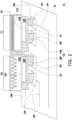
- FIG. 2 is a schematic diagram of an electronic device of an embodiment of the disclosure.
- the electronic device 10 in FIG. 2 includes a circuit substrate 20 and a light emitting chip 100.
- the light emitting chip 100 is disposed on the circuit substrate 20, and the light emitting chip 100 is the light emitting chip 100 described in FIG. 1 . Therefore, the specific structure of the light emitting chip 100 may refer to the related description of FIG. 1 .
- the light emitting chip 100 may include a first light emitting diode 110 and a second light emitting diode 120 connected in series.
- the electrode 118N of the first light emitting diode 110 is connected to the electrode 128P of the second light emitting diode 120 to form an integrated electrode 140, to realize the series connection of the first light emitting diode 110 and the second light emitting diode 120.
- the circuit substrate 20 may have a pad 22N, a pad 22P, a transmission line 24N connected to the pad 22N, and a transmission line 24P connected to the pad 22P.
- the electrode 118P of the first light emitting diode 110 is bonded to the pad 22P, and the electrode 128N of the second light emitting diode 110 is bonded to the pad 22N.
- the circuit substrate 20 may transmit electrical signals to the pad 22N and the pad 22P through the transmission line 24N and the transmission line 24P, thereby generating a driving current in the light emitting chip 100 so that the first light emitting diode 110 and the second light emitting diode 120 emit light.
- the driving current may be transmitted between the pad 22N and the pad 22P through the electrode 128N of the second light emitting diode 120, the first semiconductor layer 122N of the second light emitting diode 120, the light emitting layer 122Q of the second light emitting diode 120, the second semiconductor layer 122P of the second light emitting diode 120, the ohmic contact layer 116 of the second light emitting diode 126, an integrated electrode 140 (including the electrode 128P of the second light emitting diode 120 and the electrode 118N of the first light emitting diode 110), the first semiconductor layer 112N of the first light emitting diode 110, the light emitting layer 112Q of the first light emitting diode 110, the second semiconductor layer 112P of the first light emitting diode 110, the ohmic contact layer 116 of the first light emitting diode 110, and the electrode 118P of the first light emitting diode 110.
- the circuit substrate 20 may further include a pad 26N and a pad 26P.
- the electrode 118N of the first light emitting diode 110 may be bonded to the pad 26N
- the electrode 128P of the second light emitting diode 120 may be bonded to the pad 26P.
- the pad 26N and the pad 26P may be pads that are not connected to other pixel circuits. In some embodiments, bonding the electrode 118N to the pad 26N and the electrode 128N to the pad 26P facilitates stabilizing the connection between the light emitting chip 100 and the circuit substrate 20. In some embodiments, at least one of the pad 26N and the pad 26P may be omitted, or integrated into a single pad pattern.
- the circuit substrate 20 further includes the pixel circuit 30 shown in FIG. 3 , and the transmission line 24N and the transmission line 24P may be configured to electrically connect the pixel circuit 30 to the first light emitting diode 110 and the second light emitting diode 120 connected in series of the light emitting chip 100.
- FIG. 3 is a schematic diagram of a pixel circuit of an embodiment of the disclosure.
- the pixel circuit 30 may be connected to the scan line SL, the data line DL and the control line EM, and includes a transistor T1, a transistor T2, a transistor T3 and a capacitor C.
- the pixel circuit 30 is a driving circuit with three transistors and one capacitor (3T1C), but not limited thereto.
- the gate of the transistor T1 is connected to the scan line SL, and the other two terminals are respectively connected to the data line DL and the node N1.
- the two terminals of the capacitor C are respectively connected to the node N1 and the node N2.
- the node N2 may be connected to a power supply VDD.
- the gate of the transistor T2 is connected to the node N1, and the other two terminals are respectively connected to the node N2 and the transistor T3, that is, the two terminals of the capacitor C are respectively electrically connected to the gate of the transistor T2 and one of the other two terminals of transistor T2.
- the gate of the transistor T3 is connected to the control line EM, and the other two terminals are respectively connected to the transistor T2 and the light emitting chip 100.
- One terminal of the light emitting chip 100 (e.g., an electrode of one of the first light emitting diode 110 and the second light emitting diode 120) is connected to the transistor T3, and the other terminal (e.g., an electrode of the other one of the first light emitting diode 110 and the second light emitting diode 120) is connected to the power supply VSS.
- the pixel circuit 30 may be electrically connected to the first light emitting diode 110 and the second light emitting diode 120 connected in series to provide a driving current so that the first light emitting diode 110 and the second light emitting diode 120 emit light.
- FIG. 4 is a schematic diagram of a light emitting chip disposed in an electronic device of an embodiment of the disclosure.
- the light emitting chip 200 is similar to the aforementioned light emitting chip 100 and includes a first light emitting diode 110 and a second light emitting diode 220. Since the first light emitting diode 110 in this embodiment may be the same or similar in structure to the first light emitting diode 110 in FIG. 1 , the second light emitting diode 220 may be similar in structure to the second light emitting diode 120 in FIG. 1 . Therefore, details of each portion of the first light emitting diode 110 and the second light emitting diode 120 in this embodiment are not repeated herein.
- the first light emitting diode 110 has a first light distribution curve
- the second light emitting diode 220 has a second light distribution curve
- the first light distribution curve is different from the second light distribution curve. Therefore, the overall light emitting effect of the light emitting chip 200 may not be limited to the design of a single light emitting diode.
- the first light distribution curve of the first light emitting diode 110 has a maximum brightness at a first angle
- the second light distribution curve of the second light emitting diode 220 has a maximum brightness at a second angle
- the first angle is different from the second angle.
- the first light distribution curve of the first light emitting diode 110 has a first beam angle corresponding to 50% of the maximum brightness
- the second light distribution curve of the second light emitting diode 220 has a second beam angle corresponding to 50% of the maximum brightness
- the first beam angle and the second beam angle may have different angle ranges. In this way, the electronic device using the light emitting chip 100 may display corresponding display brightness in different angle intervals.
- Designers may use the designs of the first light emitting diode 110 and the second light emitting diode 220 to realize different light emitting effects.
- the main difference between the light emitting chip 200 in this embodiment and the light emitting chip 100 in FIG. 1 is that the electrode 118N of the first light emitting diode 110 and the electrode 228N of the second light emitting diode 220 may be integrated into an integrated electrode 240. That is, the first semiconductor layer 112N of the first light emitting diode 110 is disposed adjacent to the second semiconductor layer 122N of the second light emitting diode 220, and is electrically connected through the integrated electrode 240. In this way, the first light emitting diode 110 and the second light emitting diode 220 may form a common electrode double crystal grain structure.
- first light emitting diode 110 and the second light emitting diode 220 may be flipped laterally, so that the P pole of the first light emitting diode 110 and the P pole of the second light emitting diode 220 are disposed adjacent to each other, and the P pole of the first light emitting diode 110 may be electrically connected to the P pole of the second light emitting diode 220, thereby forming another type of common electrode double crystal grain structure.
- FIG. 5 is a schematic diagram of an electronic device of an embodiment of the disclosure.
- the electronic device 40 in FIG. 5 includes a circuit substrate 50 and a light emitting chip 200.
- the light emitting chip 200 is disposed on the circuit substrate 50, and the light emitting chip 200 is the light emitting chip 200 described in FIG. 4 . Therefore, the specific structure of the light emitting chip 200 may refer to the related description of FIG. 1 .
- the circuit substrate 50 may include a pad 52N1, a pad 52N2, a pad 52P1, and a pad 52P2.
- the pad 52N1 is disposed as a pair with the pad 52P1, and the pad 52N2 is disposed as a pair with the pad 52P2.
- the light emitting chip 200 includes a first light emitting diode 110 and a second light emitting diode 220.
- the electrode 118P of the first light emitting diode 110 is connected to the pad 52P1, and the electrode 118N of the first light emitting diode 110 is connected to the pad 52N1.
- the electrode 228P of the second light emitting diode 220 is connected to the pad 52P2, and the electrode 228N of the second light emitting diode 220 is connected to the pad 52N2.
- the circuit substrate 50 further includes a transmission line 54N, a transmission line 54P1, and a transmission line 54P2.
- the transmission line 54N is connected to the pad 52N1 and the pad 52N2. That is, the pad 52N1 and the pad 52N2 share the transmission line 54N.
- the transmission line 54P1 and the transmission line 54P2 are respectively connected to the pad 52P1 and the pad 52P2.
- the transmission line 54N, the transmission line 54P1 and the transmission line 54P2 may be configured to connect the first light emitting diode 110 and the second light emitting diode 220 to corresponding pixel circuits.
- FIG. 6 is a schematic diagram of a pixel circuit disposed on a circuit substrate of an embodiment of the disclosure.
- the pixel circuit 60 may include a first pixel circuit 62 and a second pixel circuit 64, the first pixel circuit 62 is electrically connected to the first light emitting diode 110 and the second pixel circuit 64 is electrically connected to the second light emitting diode 220. It should be noted that, in some embodiments, a sub-pixel may include both the first pixel circuit 62 and the second pixel circuit 64, while in other embodiments, a sub-pixel only includes one of the first pixel circuit 62 and the second pixel circuit 64.
- the first pixel circuit 62 may be connected to the scan line SL, the data line DL1 and the control line EM, and includes a transistor T1, a transistor T2, a transistor T3 and a capacitor C1.
- the first pixel circuit 62 is a driving circuit with three transistors and one capacitor (3T1C), but not limited thereto.
- the gate of the transistor T1 is connected to the scan line SL, and the other two terminals are respectively connected to the data line DL1 and the node N1.
- the two terminals of the capacitor C1 are respectively connected to the node N1 and the node N2.
- the node N2 may be connected to a power supply VDD.
- the gate of the transistor T2 is connected to the node N1, and the other two terminals are respectively connected to the node N2 and the transistor T3, that is, the two terminals of the capacitor C1 are respectively electrically connected to the gate of the transistor T2 and one of the other two terminals of transistor T2.
- the gate of the transistor T3 is connected to the control line EM, and the other two terminals are respectively connected to the transistor T2 and the first light emitting diode 110 of the light emitting chip 200.
- One terminal (e.g., the electrode 118P) of the first light emitting diode 110 is connected to the transistor T3, and the other terminal (e.g., the electrode 118N) is connected to the power supply VSS.
- the second pixel circuit 64 may be connected to the scan line SL, the data line DL2 and the control line EM, and includes a transistor T4, a transistor T5, a transistor T6, and a capacitor C2.
- the second pixel circuit 64 is a driving circuit with three transistors and one capacitor (3T1C), but not limited thereto.
- the gate of the transistor T4 is connected to the scan line SL, and the other two terminals are respectively connected to the data line DL2 and the node N3.
- the two terminals of the capacitor C2 are respectively connected to the node N3 and the node N4.
- the node N4 may be connected to a power supply VDD.
- the gate of the transistor T5 is connected to the node N3, and the other two terminals are respectively connected to the node N4 and the transistor T6, that is, the two terminals of the capacitor C2 are respectively electrically connected to the gate of the transistor T5 and one of the other two terminals of transistor T5.
- the gate of the transistor T6 is connected to the control line EM, and the other two terminals are respectively connected to the transistor T5 and the second light emitting diode 220 of the light emitting chip 200.
- One terminal (e.g., the electrode 228P) of the second light emitting diode 220 is connected to the transistor T6, and the other terminal (e.g., the electrode 228N) is connected to the power supply VSS.
- the pad 52P1 and the transmission line 54P1 may be configured to electrically connect the electrode 118P of the first light emitting diode 110 to the transistor T3 of the first pixel circuit 62.
- the pad 52P2 and the transmission line 54P2 may be used to electrically connect the electrode 228P of the second light emitting diode 220 to the transistor T6 of the second pixel circuit 64.
- the transmission line 54N may be configured to electrically connect the electrode 118N of the first light emitting diode 110 and the electrode 228N of the second light emitting diode 220 to the power supply VSS.
- the electrode 118N of the first light emitting diode 110 and the electrode 228N of the second light emitting diode 220 may share the transmission line 54N.
- the electrode 118N and the electrode 228N are integrated into the integrated electrode 240, one of the pad 52N1 and the pad 52N2 may be omitted, and the pixel circuit 60 may still generate the required driving current in the first light emitting diode 110 and the second light emitting diode 220.
- the transmission line 54N may be selectively connected to only one of the pad 52N1 and the pad 52N2.
- the pad 52N1 and the pad 52N2 may be integrated into a single integrated pad without being limited to two independent pads.
- the pixel circuit 60 in FIG. 6 may enable the first light emitting diode 110 and the second light emitting diode 220 to emit light at the same time or not at the same time.
- the first pixel circuit 62 and the second pixel circuit 64 may respectively receive independent signals from the data line DL1 and the data line DL2. Therefore, when the data line DL1 enables the first pixel circuit 62 such that the first light emitting diode 110 emits light, the signal on the data line DL2 may enable the second pixel circuit 64 such that the second light emitting diode 220 does not emit light, and vice versa.
- the signals on the data line DL1 and the data line DL2 may enable the first light emitting diode 110 and the second light emitting diode 220 to emit light at the same time.
- the first light distribution curve of the first light emitting diode 110 is different from the second light distribution curve of the second light emitting diode 220. Therefore, the light emitting chip 200 may provide various light emitting effects by emitting light independently with the first light emitting diode 110, emitting light independently with the second light emitting diode 220, and emitting light simultaneously with the first light emitting diode 110 and the second light emitting diode 220.
- the light emitting effect of the light emitting chip 200 depends on the first light distribution curve.
- the light emitting effect of the light emitting chip 200 depends on the second light distribution curve.
- the light emitting effect of the light emitting chip 200 is the result of combining the first light distribution curve and the second light distribution curve. In this way, the light emitting chip 200 may provide at least three light emitting modes.
- FIG. 7 is a simulation diagram of the light emitting effect of the light emitting chip of an embodiment of the disclosure.
- the first light distribution curve DC1 and the second light distribution curve are distributed in polar coordinates.
- the first light distribution curve DC1 is, for example, the light distribution curve of one of the light emitting diodes (e.g., the first light emitting diode 110) in the light emitting chip 100 or 200
- the second light distribution curve DC2 is, for example, the light distribution curve of another one of the light emitting diodes (e.g., the second light emitting diode 120 or 220). It may be seen from FIG. 7 that the two light emitting diodes of the light emitting chip 100 or 200 have different light distribution curves.
- the first light distribution curve DC1 and the second light distribution curve DC2 in FIG. 7 are used for illustration only.
- the light distribution curves of the two light emitting diodes of the light emitting chip 100 or 200 show that the first light distribution curve has a first beam angle corresponding to 50% of the maximum brightness, the second light distribution curve has a second beam angle corresponding to 50% of the maximum brightness, and the first beam angle and the second beam angle fall in different angle intervals.
- the light distribution curves of the two light emitting diodes of the light emitting chip 100 or 200 show that the first light distribution curve has a maximum brightness at a first angle, and the second light distribution curve has a maximum brightness at a second angle, and the first angle is different from the second angle.
- the first light distribution curve DC1 and the second light distribution curve DC2 are the light distribution curves of the first light emitting diode 110 and the second light emitting diode 220 in FIG. 5
- the first light distribution curve DC1 has a maximum brightness at a clockwise orientation angle (i.e., taking the vertical downward line in FIG. 7 as an angle of 0 degrees, the angle measured clockwise to the left) of about 60 degrees (the first angle) and a counterclockwise orientation angle (i.e., taking the vertical downward line in FIG. 7 as an angle of 0 degrees, the angle measured counterclockwise to the right) of about 60 degrees (the first angle).
- the second light distribution curve DC2 has a maximum brightness at a counterclockwise orientation angle of about 65 degrees (the second angle).
- the first light distribution curve DC1 has a first beam angle A1 defined by 50% of the maximum brightness
- the second light distribution curve DC2 has a second beam angle A2 defined by 50% of the maximum brightness. More specifically, in this embodiment, in the angle range from the clockwise orientation angle of about 75 degrees to the counterclockwise orientation angle of about 75 degrees, the brightness of the light emitted by the first light emitting diode 110 is greater than or equal to 50% of the maximum brightness value, so the first beam angle A1 is about 150 degrees (equal to 75 degrees plus 75 degrees).
- the brightness of the light emitted by the second light emitting diode 220 is greater than or equal to 50% of the maximum brightness value, so the second beam angle A2 is about 47 degrees (equal to 72 degrees minus 25 degrees). Therefore, the first beam angle A1 is different from the second beam angle A2, and the first light distribution curve DC1 and the second light distribution curve DC2 may provide different light emitting effects.
- the first light distribution curve DC 1 and the second light distribution curve DC2 shown in FIG. 7 are just examples, and the light distribution curves presented by the two light emitting diodes in the disclosure are not limited thereto.
- the electronic device 40 may provide a light emitting effect such as the first light distribution curve DC1, a light emitting effect such as the second light distribution curve DC2, and a light emitting effect integrating the first light distribution curve DC 1 and the second light distribution curve DC2. Therefore, the electronic device 40 may provide various light emitting modes to meet different application requirements.
- the electronic device has a double crystal grain light emitting chip, and the first light emitting diode and the second light emitting diode integrated in the light emitting chip have different light distribution curves. Therefore, the light emitting effect of the electronic device is not limited by a single light emitting diode, but may be adjusted according to different requirements. In some embodiments of the electronic device, the first light emitting diode and the second light emitting diode integrated into a single light emitting chip may emit light at different times or at the same time, so that the electronic device may provide a variety of light emitting modes and has higher application flexibility.
Landscapes
- Led Devices (AREA)
- Led Device Packages (AREA)
Abstract
Description
- The disclosure relates to an electronic device.
- The application fields of electronic devices are becoming more and more popular. Therefore, corresponding to different applications, the electronic devices need to provide different functions. For example, in different situations, electronic devices are required to provide different lighting effects. Therefore, the design of an electronic device is required to be continuously updated and/or adjusted.
- According to an embodiment of the disclosure, an electronic device includes a circuit substrate and a light emitting chip. The light emitting chip is disposed on the circuit substrate, and the light emitting chip includes a first light emitting diode and a second light emitting diode connected to each other. The first light emitting diode has a first light distribution curve, the second light emitting diode has a second light distribution curve, and the first light distribution curve is different from the second light distribution curve.
-
-
FIG. 1 is a schematic diagram of a light emitting chip disposed in an electronic device of an embodiment of the disclosure. -
FIG. 2 is a schematic diagram of an electronic device of an embodiment of the disclosure. -
FIG. 3 is a schematic diagram of a pixel circuit of an embodiment of the disclosure. -
FIG. 4 is a schematic diagram of a light emitting chip disposed in an electronic device of an embodiment of the disclosure. -
FIG. 5 is a schematic diagram of an electronic device of an embodiment of the disclosure. -
FIG. 6 is a schematic diagram of a pixel circuit disposed on a circuit substrate of an embodiment of the disclosure. -
FIG. 7 is a simulation diagram of the light emitting effect of the light emitting chip of an embodiment of the disclosure. - The disclosure may be understood by referring to the following detailed description in conjunction with the accompanying drawings. It should be noted that, for the ease of understanding by the readers and for the brevity of the accompanying drawings, multiple drawings in the disclosure only depict a portion of the electronic device, and the specific elements in the drawings are not drawn according to the actual scale. In addition, the number and size of each of the elements in the figures are for illustration purposes only, and are not intended to limit the scope of the disclosure.
- Certain terms may be used throughout the disclosure and the appended claims to refer to specific elements. It should be understood by those skilled in the art that electronic apparatus manufacturers may refer to the same elements by different names. The disclosure does not intend to distinguish between elements that have the same function but have different names.
- In the following description and claims, words such as "comprising" and "including" are open-ended words, so they should be interpreted as meaning "including but not limited to...".
- It should be understood that when an element or layer is referred to as being "disposed on" or "connected to" another element or layer, it may be directly on or directly connected to this other element or layer, or there may be an intervening element or layer in between (indirect case). In contrast, when an element is referred to as being "directly on" or "directly connected to" another element or layer, there are no intervening elements or layers present. When an element or layer is referred to as being "electrically connected" to another element or layer, it may be interpreted as being directly or indirectly electrically connected.
- The terms "about", "equal to", "equal" or "same", "substantially" or "generally" are interpreted as within ±20% of a given value or range, or interpreted as within ±10%, ±5%, ±3%, ±2%, ±1%, or ±0.5% of the given value or range.
- Although the terms "first", "second", "third" ... may be used to describe various constituent elements, the constituent elements are not limited by the terms. The terms are only used to distinguish a single constituent element from other constituent elements in the specification. The same terms may not be used in the claim, but replaced by first, second, third... according to the order in which the elements are declared in the claim. Therefore, the first constituent element in the following description may be referred to as the second constituent element in the claim.
- The electrical connection or coupling described in the disclosure may refer to direct connection or indirect connection. In the case of a direct connection, the terminal points of two elements on a circuit directly connect to each other, or connect to each other through a conductive wire. In the case of indirect connection, a switch, a diode, a capacitor, an inductor, a resistor, other suitable elements, or a combination thereof, but not limited therein, is between the terminal points of two elements on a circuit.
- In the disclosure, the length, width, thickness, height, or area, or the distance or spacing between elements may be measured by using an optical microscope (OM), a scanning electron microscope (SEM), a film thickness profilometer (α-step), an ellipsometer, or other suitable methods. In detail, according to some embodiments, a scanning electron microscope may be used to obtain a cross-sectional structure image including the component to be measured, and measure the width, thickness, height, or area of each component, or the distance or spacing between elements, but not limited thereto. Furthermore, the terms "a given range is from a first value to a second value", "a given range is within a range from the first value to the second value" means that the given range includes the first value, the second value, and other values in between. If a first direction is perpendicular to a second direction, an angle between the first direction and the second direction may be between 80 degrees and 100 degrees; if the first direction is parallel to the second direction, an angle between the first direction and the second direction may be between 0 degrees and 10 degrees.
- Unless otherwise defined, all terms (including technical and scientific terms) used herein may have the same meaning as commonly understood by one of ordinary skill in the art to which this disclosure belongs. It is understood that these terms, such as those defined in commonly used dictionaries, should be interpreted as having meanings consistent with the relevant art and the background or context of the disclosure, and should not be interpreted in an idealized or overly formal manner, unless otherwise defined in the embodiments of the disclosure.
- In the disclosure, an electronic device may include a display device, a light emitting device, a sensing device, or a splicing device, but not limited thereto. The electronic device may be a bendable or flexible electronic device. The display device may be a non-self-luminous display device or a self-luminous display device. The sensing device may be a sensing device for sensing capacitance, light, heat or ultrasonic waves, but not limited thereto. In the disclosure, electronic parts may include passive elements and active elements, such as a chip, a capacitor, a resistor, an inductor, a diode, a transistor, and the like. The diode may include a light emitting diode (LED) or a photodiode, but not limited thereto. The light emitting diode may include, for example, an organic light emitting diode (OLED), a mini light emitting diode (mini LED), a micro light emitting diode (micro LED), or a quantum dot light emitting diode (quantum dot LED), but not limited thereto. In the disclosure, a display panel may include self-luminous or non-self-luminous panels. The self-luminous panel may include, for example, an organic light emitting diode (OLED), a mini light emitting diode (mini LED), or a micro light emitting diode (micro LED), but not limited thereto. The non-self-luminous panel includes, for example, liquid crystal, or other suitable materials. It should be noted that, the electronic device may be any arrangement and combination of the foregoing, but not limited thereto. Hereinafter, a splicing device is used to illustrate the disclosure, but the disclosure is not limited thereto.
- It should be noted that the technical solutions provided by the different embodiments hereinafter may be replaced, combined, or mixed with one another, so as to constitute another embodiment without violating the spirit of the disclosure.
-
FIG. 1 is a schematic diagram of a light emitting chip disposed in an electronic device of an embodiment of the disclosure. InFIG. 1 , alight emitting chip 100 includes a firstlight emitting diode 110 and a secondlight emitting diode 120 connected to each other. In this embodiment, thelight emitting chip 100 may further include aprotective layer 130 covering the firstlight emitting diode 110 and the secondlight emitting diode 120. The material of theprotective layer 130 may include dielectric materials, such as silicon oxide, silicon nitride, silicon oxynitride, and the like. Theprotective layer 130 may be continuously extended between the firstlight emitting diode 110 and the secondlight emitting diode 120, so as to wrap the firstlight emitting diode 110 and the secondlight emitting diode 120 into a singlelight emitting chip 100. In some embodiments, the firstlight emitting diode 110 and the secondlight emitting diode 120 may be fabricated on the same substrate with a spacing distance DS between them, so that thelight emitting chip 100 has a small volume. In some embodiments, the spacing distance DS, for example, may be less than or equal to 10mm (0 <DS≦ 10mm). - The first
light emitting diode 110 and the secondlight emitting diode 120 have different characteristics. For example, the firstlight emitting diode 110 has a first light distribution curve, the secondlight emitting diode 120 has a second light distribution curve, and the first light distribution curve is different from the second light distribution curve. In this way, the firstlight emitting diode 110 and the secondlight emitting diode 120 integrated into a singlelight emitting chip 100 may provide a composite light distribution effect to meet different usage requirements. In some embodiments, multiplelight emitting chips 100 may be arranged in an array and applied to an electronic device to provide the function of displaying an image, thereby realizing a display panel, a display, and the like. - As shown in
FIG. 7 , in some embodiments, the first light distribution curve of the firstlight emitting diode 110 has a maximum brightness at a first angle, and the second light distribution curve of the secondlight emitting diode 120 has a maximum brightness at a second angle, and the first angle is different from the second angle. In this way, the electronic device using thelight emitting chip 100 may provide corresponding display brightness at the first angle and the second angle according to the usage requirements. In some embodiments, the first light distribution curve of the firstlight emitting diode 110 has a first beam angle corresponding to 50% of the maximum brightness, the second light distribution curve of the secondlight emitting diode 120 has a second beam angle corresponding to 50% of the maximum brightness, and the first beam angle and the second beam angle may fall in different angle intervals. In this way, the electronic device using thelight emitting chip 100 may display corresponding display brightness in different angle intervals. - The first
light emitting diode 110 includes afirst semiconductor stack 112 and a one-dimensional photonic crystal 114, in which the one-dimensional photonic crystal 114 is disposed on thefirst semiconductor stack 112. For example, thefirst semiconductor stack 112 includes afirst semiconductor layer 112N, alight emitting layer 112Q and asecond semiconductor layer 112P, and thelight emitting layer 112Q is disposed between thefirst semiconductor layer 112N and thesecond semiconductor layer 112P. Thefirst semiconductor layer 112N and thesecond semiconductor layer 112P have different conductivity types. In some embodiments, thefirst semiconductor layer 112N is, for example, an N-type semiconductor layer, and thesecond semiconductor layer 112P is, for example, a P-type semiconductor layer, but not limited thereto. Thelight emitting layer 112Q includes, for example, a single-layer quantum well or a multi-layer quantum well structure. The one-dimensional photonic crystal 114 is disposed on thefirst semiconductor layer 112N of thefirst semiconductor stack 112. In other words, the one-dimensional photonic crystal 114 and thelight emitting layer 112Q are located on opposite sides of thefirst semiconductor layer 112N. Alternatively, the one-dimensional photonic crystal 114 is separated from thelight emitting layer 112Q by thefirst semiconductor layer 112N. In some embodiments, the one-dimensional photonic crystal 114 may be embedded in thefirst semiconductor layer 112N. That is, a portion of thefirst semiconductor layer 112N exists between the one-dimensional photonic crystal 114 and the light emitting surface 1105 of the firstlight emitting diode 110. Therefore, the one-dimensional photonic crystal 114 may not be exposed on thelight emitting surface 110S. - As shown in
FIG. 1 , the lateral dimension of thefirst semiconductor layer 112N exceeds the lateral dimension of thesecond semiconductor layer 112P so that the firstlight emitting diode 110 forms a stepped structure, but not limited thereto. The firstlight emitting diode 110 further includes anohmic contact layer 116 disposed on the surface of thesecond semiconductor layer 112P. Theprotective layer 130 has anopening 132 and anopening 134. The firstlight emitting diode 110 further includes anelectrode 118N and anelectrode 118P. Theelectrode 118N and theelectrode 118P are disposed on theprotective layer 130 and separated from each other to avoid short circuit between the two. Theelectrode 118N fills theopening 132 and contacts thefirst semiconductor layer 112N to be electrically connected to thefirst semiconductor layer 112N, and theelectrode 118P fills theopening 134 and is electrically connected to thesecond semiconductor layer 112P through theohmic contact layer 116. Here, theelectrode 118N may be understood as an N pole, and theelectrode 118P may be understood as a P pole. In some embodiments, the surface of thefirst semiconductor layer 112N may be further provided with an ohmic contact layer (not shown), and theelectrode 118N filling theopening 132 may contact the ohmic contact layer on thefirst semiconductor layer 112N. In some embodiments, theohmic contact layer 116 may be omitted so that theelectrode 118P directly contacts thesecond semiconductor layer 112P at theopening 134. - The one-
dimensional photonic crystal 114 may include multiple patterned Braggreflective layers reflective layers reflective layers reflective layers reflective layers reflective layers light emitting diode 110 may be greater than 3 or less than 3, and is not limited to the number shown in the drawing. - In addition, the first
light emitting diode 110 has alight emitting surface 110S, and theprotective layer 130 does not cover thelight emitting surface 110S so that thelight emitting surface 110S is exposed. In this embodiment, thelight emitting surface 110S may have multiple protrusions, for example, presenting a prism-shaped outline, but not limited thereto. Theelectrodes light emitting diode 110 may be connected to corresponding pixel circuits to generate a driving current in the firstlight emitting diode 110 so that thelight emitting layer 112Q emits light. The light emitted from thelight emitting layer 112Q may pass through the one-dimensional photonic crystal 114 while traveling toward thelight emitting surface 110S. Each sub-layer in the one-dimensional photonic crystal 114 may be arranged according to a specific rule according to requirements, so as to affect the progress of light. That is, the one-dimensional photonic crystal 114 may distribute the distribution of light. Therefore, the first light distribution curve of the firstlight emitting diode 110 may be determined by the properties in regards to light of the one-dimensional photonic crystal 114. - The second
light emitting diode 120 includes asecond semiconductor stack 122 and a two-dimensional photonic crystal 124, in which the two-dimensional photonic crystal 124 is disposed on thesecond semiconductor stack 122. For example, thesecond semiconductor stack 122 includes afirst semiconductor layer 122N, alight emitting layer 122Q and asecond semiconductor layer 122P, and thelight emitting layer 122Q is disposed between thefirst semiconductor layer 122N and thesecond semiconductor layer 122P. Thefirst semiconductor layer 122N and thesecond semiconductor layer 122P have different conductivity types. In some embodiments, thefirst semiconductor layer 122N is, for example, an N-type semiconductor layer, and thesecond semiconductor layer 122P is, for example, a P-type semiconductor layer, but not limited thereto. Thelight emitting layer 122Q includes, for example, a single-layer quantum well or a multi-layer quantum well structure. The two-dimensional photonic crystal 124 is disposed on a side of thefirst semiconductor layer 122N of thesecond semiconductor stack 122 distant from thelight emitting layer 122Q. In other words, the two-dimensional photonic crystal 124 and thelight emitting layer 122Q are located on opposite sides of thefirst semiconductor layer 122N. Alternatively, the two-dimensional photonic crystal 124 is separated from thelight emitting layer 122Q by thefirst semiconductor layer 122N. In some embodiments, the two-dimensional photonic crystal 124 may be embedded in thefirst semiconductor layer 122N. In other words, a portion of thefirst semiconductor layer 122N exists between the two-dimensional photonic crystal 124 and thelight emitting surface 120S of the secondlight emitting diode 120. Therefore, the two-dimensional photonic crystal 124 may not be exposed on thelight emitting surface 120S. In some other embodiments, there may be another light-transmitting layer (not shown) between thefirst semiconductor layer 122N of the secondlight emitting diode 120 and thelight emitting surface 120S, and the two-dimensional photonic crystal may be disposed on the light-transmitting layer. - As shown in
FIG. 1 , the lateral dimension of thefirst semiconductor layer 122N exceeds the lateral dimension of thesecond semiconductor layer 122P so that the secondlight emitting diode 120 forms a stepped structure, but not limited thereto. The secondlight emitting diode 120 further includes anohmic contact layer 126 disposed on the surface of thesecond semiconductor layer 122P. Theprotective layer 130 has anopening 136 and anopening 138. The secondlight emitting diode 120 further includes anelectrode 128N and anelectrode 128P. Theelectrode 128N and theelectrode 128P are disposed on theprotective layer 130 and separated from each other to avoid short circuit between the two. Theelectrode 128N fills theopening 136 and contacts thefirst semiconductor layer 122N to be electrically connected to thefirst semiconductor layer 122N, and theelectrode 128P fills theopening 138 and is electrically connected to thesecond semiconductor layer 122P through theohmic contact layer 126. Herein, theelectrode 128N may be understood as an N pole, and theelectrode 128P may be understood as a P pole. In some embodiments, thefirst semiconductor layer 122N may be further provided with an ohmic contact layer (not shown), and theelectrode 128N filling theopening 136 may contact the ohmic contact layer on thefirst semiconductor layer 122N. In some embodiments, theohmic contact layer 126 may be omitted so that theelectrode 128P directly contacts thesecond semiconductor layer 122P at theopening 138. - In
FIG. 1 , the firstlight emitting diode 110 and the secondlight emitting diode 120 are connected in series and located in the same sub-pixel. Theelectrode 118N (N pole) of the firstlight emitting diode 110 is electrically connected to theelectrode 128P (P pole) of the secondlight emitting diode 120. Specifically, theelectrode 118N of the firstlight emitting diode 110 and theelectrode 128P of the secondlight emitting diode 120 may be integrated into anintegrated electrode 140. In other words, theintegrated electrode 140 has an integrated structure and may be connected to thefirst semiconductor layer 112N of the firstlight emitting diode 110 through theopening 132 and connected to thesecond semiconductor layer 122P of the secondlight emitting diode 120 through theopening 138. Thereby, the firstlight emitting diode 110 and the secondlight emitting diode 120 are connected in series by using theintegrated electrode 140. In other words, theelectrode 118N of the firstlight emitting diode 110 and theelectrode 128P of the secondlight emitting diode 120 may be different portions of theintegrated electrode 140. - The two-
dimensional photonic crystal 124 may include multiple voids VD and materials FL having different dielectric coefficients filled in the voids VD. The voids VD may be arranged in an array or randomly distributed. In some embodiments, the feature length of the void VD (e.g., the diameter of the void VD, if the void VD is not spherical, the longest distance between any two points on the internal surface of the void VD is referred to as the feature length of the void VD) may fall within the wavelength range of visible light, for example, 400 nm to 700 nm (400 nm ≦ feature length ≦ 700 nm). The material FL filled in the void VD may be selected from the sub-layer materials used for the one-dimensional photonic crystal 114. The materials FL filled in at least two voids VD may have different dielectric coefficients. In the drawings of the disclosure, the voids VD are filled with three different densities of dots to schematically represent that the materials FL in different voids VD have different dielectric coefficients. However, these drawings are used for illustration only, and are not used to limit the embodiments of the disclosure. In some embodiments, the void structure filled with the material FL and distributed in thefirst semiconductor layer 122N may be understood as the two-dimensional photonic crystal 124. In some embodiments, at least a portion of the voids VD may be voids VD without a filler. The arrangement of the two-dimensionalphotonic crystals 124 may affect the traveling direction of light and may be configured to determine the second light distribution curve of the secondlight emitting diode 120. - In addition, the second
light emitting diode 120 has alight emitting surface 120S, and theprotective layer 130 does not cover thelight emitting surface 120S so that thelight emitting surface 120S is exposed. In this embodiment, thelight emitting surface 120S may be a rough surface or a prism surface with multiple protrusions, but not limited thereto. Theelectrodes light emitting diode 120 may be connected to corresponding pixel circuits to generate a driving current in the secondlight emitting diode 120 so that thelight emitting layer 122Q emits light. The light emitted from thelight emitting layer 122Q may pass through the two-dimensional photonic crystal 124 while traveling toward thelight emitting surface 120S. The two-dimensionalphotonic crystals 124 may be distributed with a specific rule according to requirements, thereby affecting the progress of light. In other words, the two-dimensional photonic crystal 124 may distribute the distribution of light. Therefore, the second light distribution curve of the secondlight emitting diode 120 may be determined by the properties in regards to light of the two-dimensional photonic crystal 124. - In the
light emitting chip 100, the first light distribution curve of the firstlight emitting diode 110 may be adjusted by the one-dimensional photonic crystal 114, and the second light distribution curve of the secondlight emitting diode 120 may be adjusted by the two-dimensional photonic crystal 124. Therefore, the first light distribution curve of the firstlight emitting diode 110 is different from the second light distribution curve of the secondlight emitting diode 120, so that the overall lighting effect of thelight emitting chip 100 is not limited by the structure of a single light emitting diode. In addition, the spacing distance DS between the firstlight emitting diode 110 and the secondlight emitting diode 120 forming thelight emitting chip 100 is small, so that thelight emitting chip 100 has a smaller volume. -
FIG. 2 is a schematic diagram of an electronic device of an embodiment of the disclosure. Theelectronic device 10 inFIG. 2 includes acircuit substrate 20 and alight emitting chip 100. Thelight emitting chip 100 is disposed on thecircuit substrate 20, and thelight emitting chip 100 is thelight emitting chip 100 described inFIG. 1 . Therefore, the specific structure of thelight emitting chip 100 may refer to the related description ofFIG. 1 . Referring toFIG. 1 andFIG. 2 , thelight emitting chip 100 may include a firstlight emitting diode 110 and a secondlight emitting diode 120 connected in series. Theelectrode 118N of the firstlight emitting diode 110 is connected to theelectrode 128P of the secondlight emitting diode 120 to form anintegrated electrode 140, to realize the series connection of the firstlight emitting diode 110 and the secondlight emitting diode 120. In this embodiment, thecircuit substrate 20 may have apad 22N, apad 22P, atransmission line 24N connected to thepad 22N, and atransmission line 24P connected to thepad 22P. Theelectrode 118P of the firstlight emitting diode 110 is bonded to thepad 22P, and theelectrode 128N of the secondlight emitting diode 110 is bonded to thepad 22N. Thecircuit substrate 20 may transmit electrical signals to thepad 22N and thepad 22P through thetransmission line 24N and thetransmission line 24P, thereby generating a driving current in thelight emitting chip 100 so that the firstlight emitting diode 110 and the secondlight emitting diode 120 emit light. The driving current may be transmitted between thepad 22N and thepad 22P through theelectrode 128N of the secondlight emitting diode 120, thefirst semiconductor layer 122N of the secondlight emitting diode 120, thelight emitting layer 122Q of the secondlight emitting diode 120, thesecond semiconductor layer 122P of the secondlight emitting diode 120, theohmic contact layer 116 of the secondlight emitting diode 126, an integrated electrode 140 (including theelectrode 128P of the secondlight emitting diode 120 and theelectrode 118N of the first light emitting diode 110), thefirst semiconductor layer 112N of the firstlight emitting diode 110, thelight emitting layer 112Q of the firstlight emitting diode 110, thesecond semiconductor layer 112P of the firstlight emitting diode 110, theohmic contact layer 116 of the firstlight emitting diode 110, and theelectrode 118P of the firstlight emitting diode 110. - In addition, the
circuit substrate 20 may further include apad 26N and apad 26P. Theelectrode 118N of the firstlight emitting diode 110 may be bonded to thepad 26N, and theelectrode 128P of the secondlight emitting diode 120 may be bonded to thepad 26P. Thepad 26N and thepad 26P may be pads that are not connected to other pixel circuits. In some embodiments, bonding theelectrode 118N to thepad 26N and theelectrode 128N to thepad 26P facilitates stabilizing the connection between the light emittingchip 100 and thecircuit substrate 20. In some embodiments, at least one of thepad 26N and thepad 26P may be omitted, or integrated into a single pad pattern. - In this embodiment, the
circuit substrate 20 further includes thepixel circuit 30 shown inFIG. 3 , and thetransmission line 24N and thetransmission line 24P may be configured to electrically connect thepixel circuit 30 to the firstlight emitting diode 110 and the secondlight emitting diode 120 connected in series of thelight emitting chip 100.FIG. 3 is a schematic diagram of a pixel circuit of an embodiment of the disclosure. Thepixel circuit 30 may be connected to the scan line SL, the data line DL and the control line EM, and includes a transistor T1, a transistor T2, a transistor T3 and a capacitor C. Here, thepixel circuit 30 is a driving circuit with three transistors and one capacitor (3T1C), but not limited thereto. The gate of the transistor T1 is connected to the scan line SL, and the other two terminals are respectively connected to the data line DL and the node N1. The two terminals of the capacitor C are respectively connected to the node N1 and the node N2. The node N2 may be connected to a power supply VDD. The gate of the transistor T2 is connected to the node N1, and the other two terminals are respectively connected to the node N2 and the transistor T3, that is, the two terminals of the capacitor C are respectively electrically connected to the gate of the transistor T2 and one of the other two terminals of transistor T2. The gate of the transistor T3 is connected to the control line EM, and the other two terminals are respectively connected to the transistor T2 and thelight emitting chip 100. One terminal of the light emitting chip 100 (e.g., an electrode of one of the firstlight emitting diode 110 and the second light emitting diode 120) is connected to the transistor T3, and the other terminal (e.g., an electrode of the other one of the firstlight emitting diode 110 and the second light emitting diode 120) is connected to the power supply VSS. In this way, thepixel circuit 30 may be electrically connected to the firstlight emitting diode 110 and the secondlight emitting diode 120 connected in series to provide a driving current so that the firstlight emitting diode 110 and the secondlight emitting diode 120 emit light. -
FIG. 4 is a schematic diagram of a light emitting chip disposed in an electronic device of an embodiment of the disclosure. InFIG. 4 , thelight emitting chip 200 is similar to the aforementionedlight emitting chip 100 and includes a firstlight emitting diode 110 and a secondlight emitting diode 220. Since the firstlight emitting diode 110 in this embodiment may be the same or similar in structure to the firstlight emitting diode 110 inFIG. 1 , the secondlight emitting diode 220 may be similar in structure to the secondlight emitting diode 120 inFIG. 1 . Therefore, details of each portion of the firstlight emitting diode 110 and the secondlight emitting diode 120 in this embodiment are not repeated herein. In this embodiment, the firstlight emitting diode 110 has a first light distribution curve, the secondlight emitting diode 220 has a second light distribution curve, and the first light distribution curve is different from the second light distribution curve. Therefore, the overall light emitting effect of thelight emitting chip 200 may not be limited to the design of a single light emitting diode. - In some embodiments, the first light distribution curve of the first
light emitting diode 110 has a maximum brightness at a first angle, and the second light distribution curve of the secondlight emitting diode 220 has a maximum brightness at a second angle, and the first angle is different from the second angle. In some embodiments, the first light distribution curve of the firstlight emitting diode 110 has a first beam angle corresponding to 50% of the maximum brightness, the second light distribution curve of the secondlight emitting diode 220 has a second beam angle corresponding to 50% of the maximum brightness, and the first beam angle and the second beam angle may have different angle ranges. In this way, the electronic device using thelight emitting chip 100 may display corresponding display brightness in different angle intervals. Designers may use the designs of the firstlight emitting diode 110 and the secondlight emitting diode 220 to realize different light emitting effects. - The main difference between the light emitting
chip 200 in this embodiment and thelight emitting chip 100 inFIG. 1 is that theelectrode 118N of the firstlight emitting diode 110 and theelectrode 228N of the secondlight emitting diode 220 may be integrated into anintegrated electrode 240. That is, thefirst semiconductor layer 112N of the firstlight emitting diode 110 is disposed adjacent to thesecond semiconductor layer 122N of the secondlight emitting diode 220, and is electrically connected through theintegrated electrode 240. In this way, the firstlight emitting diode 110 and the secondlight emitting diode 220 may form a common electrode double crystal grain structure. In other embodiments, the firstlight emitting diode 110 and the secondlight emitting diode 220 may be flipped laterally, so that the P pole of the firstlight emitting diode 110 and the P pole of the secondlight emitting diode 220 are disposed adjacent to each other, and the P pole of the firstlight emitting diode 110 may be electrically connected to the P pole of the secondlight emitting diode 220, thereby forming another type of common electrode double crystal grain structure. -
FIG. 5 is a schematic diagram of an electronic device of an embodiment of the disclosure. Theelectronic device 40 inFIG. 5 includes acircuit substrate 50 and alight emitting chip 200. Thelight emitting chip 200 is disposed on thecircuit substrate 50, and thelight emitting chip 200 is thelight emitting chip 200 described inFIG. 4 . Therefore, the specific structure of thelight emitting chip 200 may refer to the related description ofFIG. 1 . InFIG. 5 , thecircuit substrate 50 may include a pad 52N1, a pad 52N2, a pad 52P1, and a pad 52P2. The pad 52N1 is disposed as a pair with the pad 52P1, and the pad 52N2 is disposed as a pair with the pad 52P2. Thelight emitting chip 200 includes a firstlight emitting diode 110 and a secondlight emitting diode 220. Theelectrode 118P of the firstlight emitting diode 110 is connected to the pad 52P1, and theelectrode 118N of the firstlight emitting diode 110 is connected to the pad 52N1. In addition, theelectrode 228P of the secondlight emitting diode 220 is connected to the pad 52P2, and theelectrode 228N of the secondlight emitting diode 220 is connected to the pad 52N2. - The
circuit substrate 50 further includes atransmission line 54N, a transmission line 54P1, and a transmission line 54P2. Thetransmission line 54N is connected to the pad 52N1 and the pad 52N2. That is, the pad 52N1 and the pad 52N2 share thetransmission line 54N. The transmission line 54P1 and the transmission line 54P2 are respectively connected to the pad 52P1 and the pad 52P2. Thetransmission line 54N, the transmission line 54P1 and the transmission line 54P2 may be configured to connect the firstlight emitting diode 110 and the secondlight emitting diode 220 to corresponding pixel circuits.FIG. 6 is a schematic diagram of a pixel circuit disposed on a circuit substrate of an embodiment of the disclosure. Thepixel circuit 60 inFIG. 6 may be, for example, applied to theelectronic device 40 inFIG. 5 and specifically disposed in thecircuit substrate 50 to drive the firstlight emitting diode 110 and the secondlight emitting diode 220 of thelight emitting chip 200. Thepixel circuit 60 may include afirst pixel circuit 62 and asecond pixel circuit 64, thefirst pixel circuit 62 is electrically connected to the firstlight emitting diode 110 and thesecond pixel circuit 64 is electrically connected to the secondlight emitting diode 220. It should be noted that, in some embodiments, a sub-pixel may include both thefirst pixel circuit 62 and thesecond pixel circuit 64, while in other embodiments, a sub-pixel only includes one of thefirst pixel circuit 62 and thesecond pixel circuit 64. - The
first pixel circuit 62 may be connected to the scan line SL, the data line DL1 and the control line EM, and includes a transistor T1, a transistor T2, a transistor T3 and a capacitor C1. Here, thefirst pixel circuit 62 is a driving circuit with three transistors and one capacitor (3T1C), but not limited thereto. The gate of the transistor T1 is connected to the scan line SL, and the other two terminals are respectively connected to the data line DL1 and the node N1. The two terminals of the capacitor C1 are respectively connected to the node N1 and the node N2. The node N2 may be connected to a power supply VDD. The gate of the transistor T2 is connected to the node N1, and the other two terminals are respectively connected to the node N2 and the transistor T3, that is, the two terminals of the capacitor C1 are respectively electrically connected to the gate of the transistor T2 and one of the other two terminals of transistor T2. The gate of the transistor T3 is connected to the control line EM, and the other two terminals are respectively connected to the transistor T2 and the firstlight emitting diode 110 of thelight emitting chip 200. One terminal (e.g., theelectrode 118P) of the firstlight emitting diode 110 is connected to the transistor T3, and the other terminal (e.g., theelectrode 118N) is connected to the power supply VSS. - Similarly, the
second pixel circuit 64 may be connected to the scan line SL, the data line DL2 and the control line EM, and includes a transistor T4, a transistor T5, a transistor T6, and a capacitor C2. Here, thesecond pixel circuit 64 is a driving circuit with three transistors and one capacitor (3T1C), but not limited thereto. The gate of the transistor T4 is connected to the scan line SL, and the other two terminals are respectively connected to the data line DL2 and the node N3. The two terminals of the capacitor C2 are respectively connected to the node N3 and the node N4. The node N4 may be connected to a power supply VDD. The gate of the transistor T5 is connected to the node N3, and the other two terminals are respectively connected to the node N4 and the transistor T6, that is, the two terminals of the capacitor C2 are respectively electrically connected to the gate of the transistor T5 and one of the other two terminals of transistor T5. The gate of the transistor T6 is connected to the control line EM, and the other two terminals are respectively connected to the transistor T5 and the secondlight emitting diode 220 of thelight emitting chip 200. One terminal (e.g., theelectrode 228P) of the secondlight emitting diode 220 is connected to the transistor T6, and the other terminal (e.g., theelectrode 228N) is connected to the power supply VSS. - Referring to
FIG. 5 andFIG. 6 , the pad 52P1 and the transmission line 54P1 may be configured to electrically connect theelectrode 118P of the firstlight emitting diode 110 to the transistor T3 of thefirst pixel circuit 62. The pad 52P2 and the transmission line 54P2 may be used to electrically connect theelectrode 228P of the secondlight emitting diode 220 to the transistor T6 of thesecond pixel circuit 64. In addition, thetransmission line 54N may be configured to electrically connect theelectrode 118N of the firstlight emitting diode 110 and theelectrode 228N of the secondlight emitting diode 220 to the power supply VSS. Therefore, theelectrode 118N of the firstlight emitting diode 110 and theelectrode 228N of the secondlight emitting diode 220 may share thetransmission line 54N. In some embodiments, since theelectrode 118N and theelectrode 228N are integrated into theintegrated electrode 240, one of the pad 52N1 and the pad 52N2 may be omitted, and thepixel circuit 60 may still generate the required driving current in the firstlight emitting diode 110 and the secondlight emitting diode 220. Similarly, thetransmission line 54N may be selectively connected to only one of the pad 52N1 and the pad 52N2. Alternatively, the pad 52N1 and the pad 52N2 may be integrated into a single integrated pad without being limited to two independent pads. - In some embodiments, the
pixel circuit 60 inFIG. 6 may enable the firstlight emitting diode 110 and the secondlight emitting diode 220 to emit light at the same time or not at the same time. For example, thefirst pixel circuit 62 and thesecond pixel circuit 64 may respectively receive independent signals from the data line DL1 and the data line DL2. Therefore, when the data line DL1 enables thefirst pixel circuit 62 such that the firstlight emitting diode 110 emits light, the signal on the data line DL2 may enable thesecond pixel circuit 64 such that the secondlight emitting diode 220 does not emit light, and vice versa. Alternatively, the signals on the data line DL1 and the data line DL2 may enable the firstlight emitting diode 110 and the secondlight emitting diode 220 to emit light at the same time. In this embodiment, the first light distribution curve of the firstlight emitting diode 110 is different from the second light distribution curve of the secondlight emitting diode 220. Therefore, thelight emitting chip 200 may provide various light emitting effects by emitting light independently with the firstlight emitting diode 110, emitting light independently with the secondlight emitting diode 220, and emitting light simultaneously with the firstlight emitting diode 110 and the secondlight emitting diode 220. When the firstlight emitting diode 110 independently emits light, the light emitting effect of thelight emitting chip 200 depends on the first light distribution curve. When the secondlight emitting diode 220 independently emits light, the light emitting effect of thelight emitting chip 200 depends on the second light distribution curve. When the firstlight emitting diode 110 and the secondlight emitting diode 220 emit light simultaneously, the light emitting effect of thelight emitting chip 200 is the result of combining the first light distribution curve and the second light distribution curve. In this way, thelight emitting chip 200 may provide at least three light emitting modes. -
FIG. 7 is a simulation diagram of the light emitting effect of the light emitting chip of an embodiment of the disclosure. InFIG. 7 , the first light distribution curve DC1 and the second light distribution curve are distributed in polar coordinates. In some embodiments, the first light distribution curve DC1 is, for example, the light distribution curve of one of the light emitting diodes (e.g., the first light emitting diode 110) in thelight emitting chip light emitting diode 120 or 220). It may be seen fromFIG. 7 that the two light emitting diodes of thelight emitting chip FIG. 7 are used for illustration only. In some embodiments, the light distribution curves of the two light emitting diodes of thelight emitting chip light emitting chip - In the embodiment where the first light distribution curve DC1 and the second light distribution curve DC2 are the light distribution curves of the first
light emitting diode 110 and the secondlight emitting diode 220 inFIG. 5 , as shown inFIG. 7 , the first light distribution curve DC1 has a maximum brightness at a clockwise orientation angle (i.e., taking the vertical downward line inFIG. 7 as an angle of 0 degrees, the angle measured clockwise to the left) of about 60 degrees (the first angle) and a counterclockwise orientation angle (i.e., taking the vertical downward line inFIG. 7 as an angle of 0 degrees, the angle measured counterclockwise to the right) of about 60 degrees (the first angle). The second light distribution curve DC2 has a maximum brightness at a counterclockwise orientation angle of about 65 degrees (the second angle). In addition, the first light distribution curve DC1 has a first beam angle A1 defined by 50% of the maximum brightness, and the second light distribution curve DC2 has a second beam angle A2 defined by 50% of the maximum brightness. More specifically, in this embodiment, in the angle range from the clockwise orientation angle of about 75 degrees to the counterclockwise orientation angle of about 75 degrees, the brightness of the light emitted by the firstlight emitting diode 110 is greater than or equal to 50% of the maximum brightness value, so the first beam angle A1 is about 150 degrees (equal to 75 degrees plus 75 degrees). For the secondlight emitting diode 220, in the angle range from the counterclockwise orientation angle of about 72 degrees to the counterclockwise orientation angle of about 25 degrees, the brightness of the light emitted by the secondlight emitting diode 220 is greater than or equal to 50% of the maximum brightness value, so the second beam angle A2 is about 47 degrees (equal to 72 degrees minus 25 degrees). Therefore, the first beam angle A1 is different from the second beam angle A2, and the first light distribution curve DC1 and the second light distribution curve DC2 may provide different light emitting effects. It should be noted that the first light distribution curve DC 1 and the second light distribution curve DC2 shown inFIG. 7 are just examples, and the light distribution curves presented by the two light emitting diodes in the disclosure are not limited thereto. - In the embodiment where the first light distribution curve DC1 and the second light distribution curve DC2 are the light distribution curves of the first
light emitting diode 110 and the secondlight emitting diode 220 inFIG. 5 , since the firstlight emitting diode 110 and the secondlight emitting diode 220 of theelectronic device 40 may emit light independently, theelectronic device 40 may provide a light emitting effect such as the first light distribution curve DC1, a light emitting effect such as the second light distribution curve DC2, and a light emitting effect integrating the first light distribution curve DC 1 and the second light distribution curve DC2. Therefore, theelectronic device 40 may provide various light emitting modes to meet different application requirements. - To sum up, the electronic device according to the embodiment of the disclosure has a double crystal grain light emitting chip, and the first light emitting diode and the second light emitting diode integrated in the light emitting chip have different light distribution curves. Therefore, the light emitting effect of the electronic device is not limited by a single light emitting diode, but may be adjusted according to different requirements. In some embodiments of the electronic device, the first light emitting diode and the second light emitting diode integrated into a single light emitting chip may emit light at different times or at the same time, so that the electronic device may provide a variety of light emitting modes and has higher application flexibility.
Claims (15)
- An electronic device (10), comprising:a circuit substrate (20, 50); anda light emitting chip (100, 200), disposed on the circuit substrate (20, 50), and the light emitting chip (100, 200) comprising a first light emitting diode (110) and a second light emitting diode (120, 220) connected to each other,wherein, the first light emitting diode (110) has a first light distribution curve, the second light emitting diode (120, 220) has a second light distribution curve, and the first light distribution curve is different from the second light distribution curve.
- The electronic device (10) according to claim 1, wherein the first light distribution curve has a maximum brightness at a first angle, the second light distribution curve has a maximum brightness at a second angle, and the first angle is different from the second angle.
- The electronic device (10) according to claim 1 or 2, wherein the first light distribution curve has a first beam angle defined by 50% of a maximum brightness, the second light distribution curve has a second beam angle defined by 50% of a maximum brightness, and first beam angle is different from the second beam angle.
- The electronic device (10) according to any of claims 1 to 3, wherein the first light emitting diode (110) and the second light emitting diode (120, 220) are connected in series.
- The electronic device (10) according to claim 4, wherein an N pole of the first light emitting diode (110) is electrically connected to a P pole of the second light emitting diode (120, 220).
- The electronic device (10) according to any of claims 1 to 5, wherein an N pole of the first light emitting diode (110) is electrically connected to an N pole of the second light emitting diode (120, 220).
- The electronic device (10) according to any of claims 1 to 6, wherein a P pole of the first light emitting diode (110) is electrically connected to a P pole of the second light emitting diode (120, 220).
- The electronic device (10) according to any of claims 1 to 7, wherein the first light emitting diode (110) comprises a first semiconductor stack (112) and a one-dimensional photonic crystal (114), and the one-dimensional photonic crystal (114) is disposed on the first semiconductor stack (112).
- The electronic device (10) according to claim 8, wherein the one-dimensional photonic crystal (114) comprises a plurality of patterned Bragg reflective layers.
- The electronic device (10) according to claim 8, wherein the first semiconductor stack (112) comprises a first semiconductor layer (112N), a light emitting layer (112Q) and a second semiconductor layer (112P), and the light emitting layer (112Q) is disposed between the first semiconductor layer (112N) and the second semiconductor layer (112P).
- The electronic device (10) according to any of claims 1 to 10, wherein the second light emitting diode (120, 220) comprises a second semiconductor stack (122) and a two-dimensional photonic crystal (124), and the two-dimensional photonic crystal (124) is disposed on the second semiconductor stack (122).
- The electronic device (10) according to claim 11, wherein the two-dimensional photonic crystal comprises a plurality of voids and materials with different dielectric coefficients filled in the voids.
- The electronic device (10) according to claim 11, wherein the second semiconductor stack (122) comprises a first semiconductor layer (122N), a light emitting layer (122Q) and a second semiconductor layer (122P), and the light emitting layer (122Q) is disposed between the first semiconductor layer (122N) and the second semiconductor layer (122P).
- The electronic device (10) according to claim 13, wherein the two-dimensional photonic crystal (124) and the light emitting layer (122Q) are located on opposite sides of the first semiconductor layer (122N).
- The electronic device (10) according to claim 13, wherein the two-dimensional photonic crystal (124) is embedded in the first semiconductor layer (122N).
Applications Claiming Priority (1)
| Application Number | Priority Date | Filing Date | Title |
|---|---|---|---|
| CN202211162364.0A CN117812773A (en) | 2022-09-23 | 2022-09-23 | electronic device |
Publications (1)
| Publication Number | Publication Date |
|---|---|
| EP4343866A1 true EP4343866A1 (en) | 2024-03-27 |
Family
ID=87933695
Family Applications (1)
| Application Number | Title | Priority Date | Filing Date |
|---|---|---|---|
| EP23195299.5A Pending EP4343866A1 (en) | 2022-09-23 | 2023-09-05 | Electronic device |
Country Status (4)
| Country | Link |
|---|---|
| US (1) | US20240105898A1 (en) |
| EP (1) | EP4343866A1 (en) |
| CN (1) | CN117812773A (en) |
| TW (1) | TWI904408B (en) |
Families Citing this family (1)
| Publication number | Priority date | Publication date | Assignee | Title |
|---|---|---|---|---|
| TWI916051B (en) | 2024-11-12 | 2026-02-21 | 台亞半導體股份有限公司 | Flip chip light emitting diode |
Citations (2)
| Publication number | Priority date | Publication date | Assignee | Title |
|---|---|---|---|---|
| WO2021249149A1 (en) * | 2020-06-10 | 2021-12-16 | 京东方科技集团股份有限公司 | Display substrate, manufacturing method therefor, and display device |
| US20220139999A1 (en) * | 2020-10-29 | 2022-05-05 | Samsung Electronics Co., Ltd. | Led display apparatus |
Family Cites Families (3)
| Publication number | Priority date | Publication date | Assignee | Title |
|---|---|---|---|---|
| CN105485541B (en) * | 2016-01-06 | 2019-01-01 | 山东晶泰星光电科技有限公司 | A kind of full light distribution type LED lamp production method |
| US11961938B2 (en) * | 2019-03-13 | 2024-04-16 | Epistar Corporation | Method of processing light-emitting elements, system and device using the same |
| CN115440129A (en) * | 2021-06-01 | 2022-12-06 | 南京瀚宇彩欣科技有限责任公司 | Anti-peeping backlight module |
-
2022
- 2022-09-23 CN CN202211162364.0A patent/CN117812773A/en active Pending
-
2023
- 2023-02-18 TW TW112105919A patent/TWI904408B/en active
- 2023-08-23 US US18/454,068 patent/US20240105898A1/en active Pending
- 2023-09-05 EP EP23195299.5A patent/EP4343866A1/en active Pending
Patent Citations (2)
| Publication number | Priority date | Publication date | Assignee | Title |
|---|---|---|---|---|
| WO2021249149A1 (en) * | 2020-06-10 | 2021-12-16 | 京东方科技集团股份有限公司 | Display substrate, manufacturing method therefor, and display device |
| US20220139999A1 (en) * | 2020-10-29 | 2022-05-05 | Samsung Electronics Co., Ltd. | Led display apparatus |
Also Published As
| Publication number | Publication date |
|---|---|
| US20240105898A1 (en) | 2024-03-28 |
| TW202414783A (en) | 2024-04-01 |
| TWI904408B (en) | 2025-11-11 |
| CN117812773A (en) | 2024-04-02 |
Similar Documents
| Publication | Publication Date | Title |
|---|---|---|
| CN113903268B (en) | Display device | |
| KR102488068B1 (en) | Light unit and display device comprising the same | |
| US12132072B2 (en) | Display device and method of fabricating the same | |
| KR102684757B1 (en) | Display device | |
| US11695094B2 (en) | Pixel and display device including the same | |
| CN113823661A (en) | display device | |
| CN115707288A (en) | Display device | |
| US20250126952A1 (en) | Display device | |
| CN117242576A (en) | display device | |
| CN115996613A (en) | display device | |
| KR102949693B1 (en) | Display device | |
| KR102883988B1 (en) | Display device and manufacturing method of the same | |
| US20240105898A1 (en) | Electronic device | |
| KR20250173469A (en) | Display device | |
| CN115552610A (en) | Display device | |
| CN116613183A (en) | Display device | |
| KR20230174803A (en) | display device | |
| US12453214B2 (en) | Display device | |
| CN116581138A (en) | Display device and manufacturing method thereof | |
| CN115581090A (en) | Display device | |
| CN115377139A (en) | Display device | |
| CN116097437A (en) | Display device | |
| KR20230013669A (en) | Display device and manufacturing method for thereof | |
| US20240030389A1 (en) | Display device and method of fabricating the same | |
| KR20240117681A (en) | Display device |
Legal Events
| Date | Code | Title | Description |
|---|---|---|---|
| PUAI | Public reference made under article 153(3) epc to a published international application that has entered the european phase |
Free format text: ORIGINAL CODE: 0009012 |
|
| STAA | Information on the status of an ep patent application or granted ep patent |
Free format text: STATUS: THE APPLICATION HAS BEEN PUBLISHED |
|
| AK | Designated contracting states |
Kind code of ref document: A1 Designated state(s): AL AT BE BG CH CY CZ DE DK EE ES FI FR GB GR HR HU IE IS IT LI LT LU LV MC ME MK MT NL NO PL PT RO RS SE SI SK SM TR |
|
| STAA | Information on the status of an ep patent application or granted ep patent |
Free format text: STATUS: REQUEST FOR EXAMINATION WAS MADE |
|
| 17P | Request for examination filed |
Effective date: 20240904 |
|
| RBV | Designated contracting states (corrected) |
Designated state(s): AL AT BE BG CH CY CZ DE DK EE ES FI FR GB GR HR HU IE IS IT LI LT LU LV MC ME MK MT NL NO PL PT RO RS SE SI SK SM TR |