EP4343859A1 - Photodiode modules with reduced recovery times - Google Patents
Photodiode modules with reduced recovery times Download PDFInfo
- Publication number
- EP4343859A1 EP4343859A1 EP23186621.1A EP23186621A EP4343859A1 EP 4343859 A1 EP4343859 A1 EP 4343859A1 EP 23186621 A EP23186621 A EP 23186621A EP 4343859 A1 EP4343859 A1 EP 4343859A1
- Authority
- EP
- European Patent Office
- Prior art keywords
- heating element
- photodiode
- photodiode chip
- chip
- module
- Prior art date
- Legal status (The legal status is an assumption and is not a legal conclusion. Google has not performed a legal analysis and makes no representation as to the accuracy of the status listed.)
- Pending
Links
- 238000011084 recovery Methods 0.000 title claims abstract description 15
- 238000010438 heat treatment Methods 0.000 claims abstract description 108
- 239000000835 fiber Substances 0.000 claims description 16
- 238000009529 body temperature measurement Methods 0.000 claims description 10
- 238000010586 diagram Methods 0.000 description 12
- 229910000530 Gallium indium arsenide Inorganic materials 0.000 description 11
- KXNLCSXBJCPWGL-UHFFFAOYSA-N [Ga].[As].[In] Chemical compound [Ga].[As].[In] KXNLCSXBJCPWGL-UHFFFAOYSA-N 0.000 description 11
- 238000010521 absorption reaction Methods 0.000 description 11
- 239000013307 optical fiber Substances 0.000 description 10
- 230000003287 optical effect Effects 0.000 description 9
- 230000004044 response Effects 0.000 description 9
- 239000004065 semiconductor Substances 0.000 description 9
- 230000005684 electric field Effects 0.000 description 8
- 230000006870 function Effects 0.000 description 8
- 238000000034 method Methods 0.000 description 8
- 238000000098 azimuthal photoelectron diffraction Methods 0.000 description 5
- VYPSYNLAJGMNEJ-UHFFFAOYSA-N Silicium dioxide Chemical compound O=[Si]=O VYPSYNLAJGMNEJ-UHFFFAOYSA-N 0.000 description 4
- 239000000463 material Substances 0.000 description 4
- 230000008569 process Effects 0.000 description 4
- 230000035945 sensitivity Effects 0.000 description 3
- 238000012360 testing method Methods 0.000 description 3
- 239000000969 carrier Substances 0.000 description 2
- 238000004891 communication Methods 0.000 description 2
- 238000013500 data storage Methods 0.000 description 2
- 230000005611 electricity Effects 0.000 description 2
- 239000000377 silicon dioxide Substances 0.000 description 2
- FRWYFWZENXDZMU-UHFFFAOYSA-N 2-iodoquinoline Chemical compound C1=CC=CC2=NC(I)=CC=C21 FRWYFWZENXDZMU-UHFFFAOYSA-N 0.000 description 1
- GPXJNWSHGFTCBW-UHFFFAOYSA-N Indium phosphide Chemical compound [In]#P GPXJNWSHGFTCBW-UHFFFAOYSA-N 0.000 description 1
- 229910052581 Si3N4 Inorganic materials 0.000 description 1
- 229910004205 SiNX Inorganic materials 0.000 description 1
- 230000004913 activation Effects 0.000 description 1
- 239000000853 adhesive Substances 0.000 description 1
- 230000001070 adhesive effect Effects 0.000 description 1
- 230000004075 alteration Effects 0.000 description 1
- PNEYBMLMFCGWSK-UHFFFAOYSA-N aluminium oxide Inorganic materials [O-2].[O-2].[O-2].[Al+3].[Al+3] PNEYBMLMFCGWSK-UHFFFAOYSA-N 0.000 description 1
- 230000004888 barrier function Effects 0.000 description 1
- LTPBRCUWZOMYOC-UHFFFAOYSA-N beryllium oxide Inorganic materials O=[Be] LTPBRCUWZOMYOC-UHFFFAOYSA-N 0.000 description 1
- 229910010293 ceramic material Inorganic materials 0.000 description 1
- PMHQVHHXPFUNSP-UHFFFAOYSA-M copper(1+);methylsulfanylmethane;bromide Chemical compound Br[Cu].CSC PMHQVHHXPFUNSP-UHFFFAOYSA-M 0.000 description 1
- 230000007547 defect Effects 0.000 description 1
- 229910003460 diamond Inorganic materials 0.000 description 1
- 239000010432 diamond Substances 0.000 description 1
- 230000000694 effects Effects 0.000 description 1
- 238000003780 insertion Methods 0.000 description 1
- 230000037431 insertion Effects 0.000 description 1
- 239000007769 metal material Substances 0.000 description 1
- 239000012811 non-conductive material Substances 0.000 description 1
- 230000005693 optoelectronics Effects 0.000 description 1
- 238000012545 processing Methods 0.000 description 1
- 230000005855 radiation Effects 0.000 description 1
- 230000009467 reduction Effects 0.000 description 1
- 238000002310 reflectometry Methods 0.000 description 1
- 239000000523 sample Substances 0.000 description 1
- 229910052594 sapphire Inorganic materials 0.000 description 1
- 239000010980 sapphire Substances 0.000 description 1
- 235000012239 silicon dioxide Nutrition 0.000 description 1
- HQVNEWCFYHHQES-UHFFFAOYSA-N silicon nitride Chemical compound N12[Si]34N5[Si]62N3[Si]51N64 HQVNEWCFYHHQES-UHFFFAOYSA-N 0.000 description 1
- MZLGASXMSKOWSE-UHFFFAOYSA-N tantalum nitride Chemical compound [Ta]#N MZLGASXMSKOWSE-UHFFFAOYSA-N 0.000 description 1
- 238000003466 welding Methods 0.000 description 1
Images



Classifications
-
- H—ELECTRICITY
- H10—SEMICONDUCTOR DEVICES; ELECTRIC SOLID-STATE DEVICES NOT OTHERWISE PROVIDED FOR
- H10F—INORGANIC SEMICONDUCTOR DEVICES SENSITIVE TO INFRARED RADIATION, LIGHT, ELECTROMAGNETIC RADIATION OF SHORTER WAVELENGTH OR CORPUSCULAR RADIATION
- H10F30/00—Individual radiation-sensitive semiconductor devices in which radiation controls the flow of current through the devices, e.g. photodetectors
- H10F30/20—Individual radiation-sensitive semiconductor devices in which radiation controls the flow of current through the devices, e.g. photodetectors the devices having potential barriers, e.g. phototransistors
- H10F30/21—Individual radiation-sensitive semiconductor devices in which radiation controls the flow of current through the devices, e.g. photodetectors the devices having potential barriers, e.g. phototransistors the devices being sensitive to infrared, visible or ultraviolet radiation
- H10F30/22—Individual radiation-sensitive semiconductor devices in which radiation controls the flow of current through the devices, e.g. photodetectors the devices having potential barriers, e.g. phototransistors the devices being sensitive to infrared, visible or ultraviolet radiation the devices having only one potential barrier, e.g. photodiodes
- H10F30/225—Individual radiation-sensitive semiconductor devices in which radiation controls the flow of current through the devices, e.g. photodetectors the devices having potential barriers, e.g. phototransistors the devices being sensitive to infrared, visible or ultraviolet radiation the devices having only one potential barrier, e.g. photodiodes the potential barrier working in avalanche mode, e.g. avalanche photodiodes
-
- H—ELECTRICITY
- H10—SEMICONDUCTOR DEVICES; ELECTRIC SOLID-STATE DEVICES NOT OTHERWISE PROVIDED FOR
- H10F—INORGANIC SEMICONDUCTOR DEVICES SENSITIVE TO INFRARED RADIATION, LIGHT, ELECTROMAGNETIC RADIATION OF SHORTER WAVELENGTH OR CORPUSCULAR RADIATION
- H10F77/00—Constructional details of devices covered by this subclass
- H10F77/40—Optical elements or arrangements
- H10F77/407—Optical elements or arrangements indirectly associated with the devices
-
- H—ELECTRICITY
- H10—SEMICONDUCTOR DEVICES; ELECTRIC SOLID-STATE DEVICES NOT OTHERWISE PROVIDED FOR
- H10F—INORGANIC SEMICONDUCTOR DEVICES SENSITIVE TO INFRARED RADIATION, LIGHT, ELECTROMAGNETIC RADIATION OF SHORTER WAVELENGTH OR CORPUSCULAR RADIATION
- H10F77/00—Constructional details of devices covered by this subclass
- H10F77/60—Arrangements for cooling, heating, ventilating or compensating for temperature fluctuations
-
- H—ELECTRICITY
- H10—SEMICONDUCTOR DEVICES; ELECTRIC SOLID-STATE DEVICES NOT OTHERWISE PROVIDED FOR
- H10F—INORGANIC SEMICONDUCTOR DEVICES SENSITIVE TO INFRARED RADIATION, LIGHT, ELECTROMAGNETIC RADIATION OF SHORTER WAVELENGTH OR CORPUSCULAR RADIATION
- H10F77/00—Constructional details of devices covered by this subclass
- H10F77/93—Interconnections
- H10F77/933—Interconnections for devices having potential barriers
-
- G—PHYSICS
- G02—OPTICS
- G02B—OPTICAL ELEMENTS, SYSTEMS OR APPARATUS
- G02B6/00—Light guides; Structural details of arrangements comprising light guides and other optical elements, e.g. couplings
- G02B6/24—Coupling light guides
- G02B6/42—Coupling light guides with opto-electronic elements
- G02B6/4201—Packages, e.g. shape, construction, internal or external details
- G02B6/4204—Packages, e.g. shape, construction, internal or external details the coupling comprising intermediate optical elements, e.g. lenses, holograms
-
- G—PHYSICS
- G02—OPTICS
- G02B—OPTICAL ELEMENTS, SYSTEMS OR APPARATUS
- G02B6/00—Light guides; Structural details of arrangements comprising light guides and other optical elements, e.g. couplings
- G02B6/24—Coupling light guides
- G02B6/42—Coupling light guides with opto-electronic elements
- G02B6/4201—Packages, e.g. shape, construction, internal or external details
- G02B6/4266—Thermal aspects, temperature control or temperature monitoring
-
- G—PHYSICS
- G02—OPTICS
- G02B—OPTICAL ELEMENTS, SYSTEMS OR APPARATUS
- G02B6/00—Light guides; Structural details of arrangements comprising light guides and other optical elements, e.g. couplings
- G02B6/24—Coupling light guides
- G02B6/42—Coupling light guides with opto-electronic elements
- G02B6/4292—Coupling light guides with opto-electronic elements the light guide being disconnectable from the opto-electronic element, e.g. mutually self aligning arrangements
Definitions
- An avalanche photodiode which may also be referenced as a semiconductor photodiode detector, converts light into electricity by utilizing the photoelectric effect.
- APDs often include a relatively high sensitivity and a relatively high internal gain. Additionally, APDs are often used in fiber optic communication systems as photodetectors.
- a photodiode module comprising: a photodiode chip; and a heating element to heat the photodiode chip to reduce a recovery time of the photodiode chip.
- the photodiode module may further comprise: a fiber pigtailed package enclosing the photodiode chip.
- the heating element may be positioned on a submount located adjacent to the photodiode chip.
- the photodiode module may further comprise: a first heating element contact; and a second heating element contact, wherein the first heating element contact and the second heating element contact are in electrical contact with the heating element and are positioned on the submount.
- the photodiode module may further comprise: an electrical isolator positioned between the heating element and the photodiode chip.
- the heating element may be part of the photodiode chip.
- the heating element may be to cause a decrease in recovery time of the photodiode chip.
- the photodiode module may further comprise: a thermistor positioned to detect a temperature of the heating element, the thermistor to send temperature measurements to a controller and the controller to control, by at least one hardware processor, the temperature of the heating element based on the temperature measurements.
- a photodiode module comprising: an avalanche photodiode chip; and a heating element to heat the avalanche photodiode chip to cause a recovery time of the avalanche photodiode chip to be reduced.
- the photodiode module may comprise: a fiber pigtailed package enclosing the avalanche photodiode chip.
- the photodiode module may further comprising: a submount located adjacent to the avalanche photodiode chip, wherein the heating element is positioned on the submount, adjacent to the avalanche photodiode chip.
- the photodiode module may further comprise: a first heating element contact; and a second heating element contact, wherein the first heating element contact and the second heating element contact are in electrical contact with the heating element and are positioned on the submount.
- the photodiode module may further comprise: an electrical isolator positioned between the heating element and the avalanche photodiode chip.
- the photodiode module may further comprise: a thermistor positioned to detect a temperature of the heating element, the thermistor to send temperature measurements to a controller and the controller to control the temperature of the heating element based on the temperature measurements.
- a photodiode module comprising: a photodiode chip; a heating element to heat the photodiode chip; a submount to support the photodiode chip; and a fiber pigtailed package enclosing the photodiode chip and the submount.
- the heating element may be positioned between a portion of the photodiode chip and a portion of the submount.
- the photodiode module may further comprise: an electrical isolator positioned between the heating element and the photodiode chip.
- the photodiode module may further comprise: a first heating element contact; and a second heating element contact, wherein the first heating element contact and the second heating element contact are in electrical contact with the heating element and are positioned on the submount.
- the heating element may be to heat the photodiode chip to cause a reduction in recovery time of the photodiode chip.
- the photodiode module may further comprise: a thermistor positioned to detect a temperature of the heating element, the thermistor to send temperature measurements to a controller and the controller to control, by at least one hardware processor, the temperature of the heating element based on the temperature measurements.
- optical fiber may be generalized to an optical waveguide of any type.
- An optical time-domain reflectometer (OTDR) device is an optoelectronic instrument used to characterize an optical fiber.
- An OTDR device injects a series of optical pulses into an optical fiber under test through a wavelength division multiplexing (WDM) component in order to test and monitor a network. Based on the injected optical pulses, the OTDR device may extract, from the same end of the optical fiber in which the optical pulses are injected, light that is scattered or reflected back from points along the optical fiber. The scattered or reflected light that is gathered back is used to characterize the optical fiber. For example, the scattered or reflected light that is gathered back is used to detect, locate, and measure events at any location of the optical fiber. The events may include faults at any location of the optical fiber.
- WDM wavelength division multiplexing
- OTDR device may measure attenuation uniformity and attenuation rate, segment length, bends, fiber end, and location and insertion loss of connectors, splices, or any other optical components such as splitters or multiplexers.
- low levels of light may need to be adequately measured immediately after occurrence of events such as Fresnel reflections or splitters on an optical probe pulse along an optical fiber under test.
- the light may need to be measured immediately after the occurrence of the events to avoid too long of a "dead zone," which is one of the main specifications of an OTDR device.
- a high gain and low noise avalanche photodiode e.g., an APD with high sensitivity, is often needed to adequately measure the light.
- the wavelengths of interest are mainly located in the short wavelength infrared range (typically between around 1300 nm and around 1650 nm).
- the absorption region of the semiconductor of the APD may need to have a small energy bandgap, e.g., a wavelength cutoff higher than around 1650 nm.
- indium gallium arsenide (InGaAs) is a semiconductor used as an absorption region for APDs, which has a relatively small energy bandgap.
- InGaAs indium gallium arsenide
- heterojunctions and localized p-doped regions are used to provide high levels of sensitivity.
- a high bandgap energy p-doped semiconductor with a smaller area than the absorption region area is defined as the active area of the semi-conductor structure (the high electric field area). Particularly this helps to have no electric field at the edge of the InGaAs region where defects in the semiconductor could lead to noise if localized in the high electric field region.
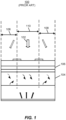
- FIG. 1 shows a cross-sectional diagram of a conventional APD 100.
- the APD 100 in Figure 1 shows the principle of the absorption of photons 102 in a front side illuminated InGaAs APD semiconductor structure.
- photons 102 are absorbed in the active absorption region 104, which may be made of InGaAs, and dissociated into electron and hole carriers.
- the active absorption region 104 which may be made of InGaAs, and dissociated into electron and hole carriers.
- Those last carriers are multiplied in the multiplication region 106, which may be made of indium phosphide (InP), to give rise to an internal gain.
- the active absorption region 104 is delimited by a localized p-doped region (so-called planar structure).
- T_BW is an intrinsic time response of the APD 100 and may mainly be related to the bandwidth of the APD 100. This time response may be made to be negligible compared to the other two time responses by selecting an APD 100 with a sufficiently high bandwidth, e.g., a few GHz.
- T_LEF is a time response of the photons that are directly absorbed in low electric field areas 108 (or at the edge of high electric field area 110). This time response may be important for a large beam compared to the high electric field area 110 or for beams with optical aberrations.
- T_NDA is a time response of the photons that go through the high electric field area 110 but are not directly absorbed.
- an InGaAs APD 100 may have a typical absorption efficiency of about 85% at 1550 nm and thus 15% of the photons are not directly absorbed. Instead, those photons are reflected or backscattered by the backside of the APD 100 to partly go into the low electric field areas 108.
- the photodiode modules disclosed herein may include structures that reduce the T_NDA response time of the photodiode chips.
- the photodiode modules disclosed herein may reduce the T_NDA response time through inclusion of heating elements that are to heat the photodiode chips during usage of the photodiode chips.
- the heating elements may increase the temperatures of the photodiode chips, which may allow the quantum efficiency of the photodiode chips to increase at a given wavelength, especially near an ambient temperature wavelength cutoff, which may be around 1650 nm for InGaAs APDs.
- the quantum efficiency may be increased because the quantum efficiency increases as a function of wavelength.
- the increase in the quantum efficiency reduces or improves the recovery times of the photodiode chips.
- the heating elements may be positioned between the photodiode chips and submounts of the photodiode modules. In some examples, the heating elements are positioned on the submounts, while in other examples, the heating elements are formed as part of the photodiode chips. In some examples, the photodiode module includes a fiber pigtailed package that encloses the photodiode chips and the submounts.
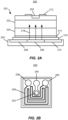
- FIG. 2A illustrates a diagram of a photodiode module 200, in accordance with an example of the present disclosure.
- the photodiode module 200 is depicted in Figure 2A as including a photodiode chip 202, a submount 204, and a heating element 206.
- the photodiode chip 202 may be similar to the APD 100 depicted in Figure 1 and may thus include the elements described above with respect to Figure 1 .
- the submount 204 may be formed of a thermally non-conductive material, such as a ceramic material like alumina and/or the like.
- the photodiode chip 202 may be adhered to the submount 204 through use of an adhesive, welding, and/or the like, or may be mounted to the submount 204 via a mechanical fastener.
- the heating element 206 is positioned with respect to the photodiode chip 202 to increase a temperature of at least a portion of the photodiode chip 202.
- the heating element 206 is to increase a temperature of the photodiode chip 202, or a portion of the photodiode chip 202, to a temperature that increases recovery time of the photodiode chip 202.
- the heating element 206 is to increase the temperature of the photodiode chip 202 to a sufficient level to cause a quantum efficiency of the photodiode chip 202 to be increased above a cutoff wavelength of the photodiode chip 202.
- the heating element 206 is positioned between the photodiode chip 202 and the submount 204. In some examples, the heating element 206 is formed within or on the submount 204 at an interface location adjacent to a bottom surface of the photodiode chip 202. In other examples, the heating element 206 is formed within or on the photodiode chip 202 at an interface location adjacent to a top surface of the submount 204. In any of these examples, the heating element 206 is formed of any suitable material that may become heated through receipt of electrical energy, e.g., a material that converts electrical energy into heat. For instance, the heating element may be formed of a metallic material, tantalum nitride (TaN), or the like.
- TaN tantalum nitride
- the heating element 206 is in electrical contact with a first heating element contact 208 and a second heating element contact 210.
- the first heating element contact 208 and the second heating element contact 210 are shown to be in electrical contact with an electrical energy source (not shown) such that electrical energy may be conducted through the heating element 206 via the first heating element contact 208 and the second heating element contact 210.
- the heating element 206 converts the electrical energy into heat such that heat from the heating element 206 increases a temperature of the photodiode chip 202 (or a portion of the photodiode chip 202).
- the photodiode chip 202 includes an anode 212 and a cathode 214, where the cathode 214 is near the heating element 206.
- an electrical isolator 216 may be positioned between the heating element 206 and the cathode 214.
- the electrical isolator 216 blocks or reduces the flow of electricity between the heating element 206 and the cathode 214.
- the electrical isolator 216 may enable heat to flow through the electrical isolator 216 from the heating element 206 to the cathode 214.
- the electrical isolator 216 may be formed either by a thin dielectric film or by a submount.
- the thin dielectric film may be a silicon nitride (SiNx) or a silicon dioxide (SiO 2 ) layer.
- the submount 204 may be made of any suitable material that is thermally conductive while also being electrically insulative. Examples of such suitable materials include aluminum nitride, beryllium oxide, diamond, sapphire, and/or the like.
- heat which is represented by the arrows 218, that is generated in the heating element 206, flows through the electrical isolator 216 and into the photodiode chip 202.
- the heat 218 may be conducted through the electrical isolator 216 into an active absorption region 220 of the photodiode chip 202.
- the heat 218 may also be conducted through the active absorption region 220 and into the multiplication region 222 of the photodiode chip 202.
- the heat 218 may further be conducted through the multiplication region 222 and to a p-doped area 224 of the photodiode chip 202.
- the heating element 206 has a relatively small form factor, e.g., is relatively smaller in length and width than the photodiode chip 202. In some examples, the relatively small size of the heating element 206 enables the heating element 206 to heat the photodiode chip 202 without significantly heating a fiber or an electronic board near the photodiode chip 202.
- the p-doped area 224 is relatively smaller than the active absorption region 220.
- the photodiode chip 202 is a front side illuminated avalanche photodiode chip having a heterojunction structure with a high bandgap energy p-doped semiconductor area 224 that is smaller than the absorption region 220.
- the heating element 206 may be formed or otherwise included in the photodiode chip 202.
- the heating element 206 may be formed on the top side of the photodiode chip 250 as shown in Figure 2B .
- Figure 2B shows a diagram of a photodiode chip 250, according to an example of the present disclosure.
- the photodiode chip 250 includes an active area 252 of the photodiode chip 250.
- the active area 252 may include, for instance, the elements 220-224 of the photodiode module 200 depicted in Figure 2A .
- the photodiode chip 250 is also depicted as including an anode bonding pad 254 on which an anode, e.g., anode 212, is to be bonded.
- the photodiode chip 250 is further depicted as including a heating element 256 in the form of a coiled wire that is positioned adjacent to the active area 252.
- the heating element 256 is depicted as being electrically connected to a first heating element bonding pad 258 and a second heating element bonding pad 260.
- the first heating element bonding pad 258 may be equivalent to the first heating element contact 208 and the second heating element bonding pad 260 may be equivalent to the second heating element contact 210.
- the cutoff wavelength may be defined as the wavelength where an incoming light has nearly enough energy to free an electron.
- the cutoff wavelength may be the wavelength at which all of a photon's energy goes into overcoming the work friction barrier.
- the cutoff wavelength increases with an increase in temperature. In this regard, by increasing the temperature of the photodiode chip 202 through use of the heating element 206, the cutoff wavelength of the photodiode chip 202 may be increased.
- the quantum efficiency may be defined as the ratio of the number photoelectrons released in a photoelectric process to the number of radiation quanta absorbed.
- the quantum efficiency of the wavelengths increases as temperature increases.
- the quantum efficiency of the photodiode chip 202 may also be increased.
- the Increase in the quantum efficiency of the photodiode chip 202 may also improve the recovery time of the photodiode chip 202.
- the photodiode module 400 includes a photodiode chip 402, which, in some examples, is an avalanche photodiode chip.
- the photodiode module 400 also includes a heating element 404 and a submount 406.
- the photodiode chip 402, the heating element 404, and the submount 406 are depicted as being enclosed within a fiber pigtailed package 408.
- the fiber pigtailed package 408 is a TO-can pigtailed package.
- the fiber pigtailed package 408 is depicted as positioning an end of a fiber 410 near a front side of the photodiode chip 402.
- the fiber pigtailed package 408 is also depicted as including a lens 412 or other optical device that may direct light from the fiber 410 and onto the front side of the photodiode chip 402.
- the fiber 410 which may be an optical fiber, may be butt-coupled to the photodiode chip 402.
- the photodiode module 400 may include a thermistor 414 that is positioned to detect a temperature of the heating element 404.
- the thermistor 414 is depicted as being positioned beneath the heating element 404 in the submount 406. In other examples, the thermistor 414 may be positioned at other locations.
- the thermistor 414 may send temperature measurements to a controller (not shown) of the heating element 404.
- the controller may control, by at least one hardware processor, the temperature of the heating element 404 based on the temperature measurements.
- the controller may be an external proportional, integral, derivative (PID) temperature controller.
- FIG. 5 shows a computer system 500 that may be used with the examples described herein.
- the computer system may represent a generic platform that includes components that may be in a server or another computer system.
- the computer system 500 may be used as part of a platform for the photodiode module 200, the photodiode chip 250, and the photodiode module 400.
- the computer system 500 may execute, by a processor 502 (e.g., a single or multiple processors) or other hardware processing circuit, the methods, functions and other processes described herein.
- a processor 502 e.g., a single or multiple processors
- a computer readable medium e.g., memory 504
- a computer readable medium e.g., memory 504
- non-transitory such as hardware storage devices (e.g., RAM (random access memory), ROM (read only memory), EPROM (erasable, programmable ROM), EEPROM (electrically erasable, programmable ROM), hard drives, and flash memory).
- RAM random access memory
- ROM read only memory
- EPROM erasable, programmable ROM
- EEPROM electrically erasable, programmable ROM
- hard drives e.g., hard drives, and flash memory
- the computer system 500 may include a processor 502 that may implement or execute machine readable instructions performing some or all of the methods, functions and other processes described herein. Commands and data from the processor 502 may be communicated over a communication bus 506.
- the computer system 500 may also include a main memory 504, such as a random access memory (RAM), where the machine readable instructions and data for the processor 502 may reside during runtime, and a secondary data storage 508, which may be non-volatile and stores machine readable instructions and data.
- the memory 504 and data storage 508 are examples of computer readable mediums.
- the memory 504 may include machine readable instructions to control activation of the heating element 206, 256 during runtime and executed by the processor 502.
- the computer system 500 may include an I/O device 510, such as a keyboard, a mouse, a display, etc.
- the computer system 500 may also include a network interface 512 for connecting to a network.
- Other known electronic components may be added or substituted in the computer system.
- the processor 502 may be designated as a hardware processor.
- the processor 502 may execute operations associated with various components of an OTDR device.
Landscapes
- Light Receiving Elements (AREA)
Abstract
Description
- An avalanche photodiode (APD), which may also be referenced as a semiconductor photodiode detector, converts light into electricity by utilizing the photoelectric effect. APDs often include a relatively high sensitivity and a relatively high internal gain. Additionally, APDs are often used in fiber optic communication systems as photodetectors.
- According to an aspect of the present disclosure there is provided a photodiode module in accordance with the accompanying claims.
- According to a further aspect of the present disclosure there is provided a photodiode module comprising: a photodiode chip; and a heating element to heat the photodiode chip to reduce a recovery time of the photodiode chip.
- The photodiode module may further comprise: a fiber pigtailed package enclosing the photodiode chip. The heating element may be positioned on a submount located adjacent to the photodiode chip. The photodiode module may further comprise: a first heating element contact; and a second heating element contact, wherein the first heating element contact and the second heating element contact are in electrical contact with the heating element and are positioned on the submount. The photodiode module may further comprise: an electrical isolator positioned between the heating element and the photodiode chip. The heating element may be part of the photodiode chip. The heating element may be to cause a decrease in recovery time of the photodiode chip. The photodiode module may further comprise: a thermistor positioned to detect a temperature of the heating element, the thermistor to send temperature measurements to a controller and the controller to control, by at least one hardware processor, the temperature of the heating element based on the temperature measurements.
- According to a further aspect of the present disclosure there is provided a photodiode module comprising: an avalanche photodiode chip; and a heating element to heat the avalanche photodiode chip to cause a recovery time of the avalanche photodiode chip to be reduced.
- The photodiode module may comprise: a fiber pigtailed package enclosing the avalanche photodiode chip. The photodiode module may further comprising: a submount located adjacent to the avalanche photodiode chip, wherein the heating element is positioned on the submount, adjacent to the avalanche photodiode chip. The photodiode module may further comprise: a first heating element contact; and a second heating element contact, wherein the first heating element contact and the second heating element contact are in electrical contact with the heating element and are positioned on the submount. The photodiode module may further comprise: an electrical isolator positioned between the heating element and the avalanche photodiode chip. The photodiode module may further comprise: a thermistor positioned to detect a temperature of the heating element, the thermistor to send temperature measurements to a controller and the controller to control the temperature of the heating element based on the temperature measurements.
- According to a still further aspect of the present disclosure there is provided a photodiode module comprising: a photodiode chip; a heating element to heat the photodiode chip; a submount to support the photodiode chip; and a fiber pigtailed package enclosing the photodiode chip and the submount.
- The heating element may be positioned between a portion of the photodiode chip and a portion of the submount. The photodiode module may further comprise: an electrical isolator positioned between the heating element and the photodiode chip. The photodiode module may further comprise: a first heating element contact; and a second heating element contact, wherein the first heating element contact and the second heating element contact are in electrical contact with the heating element and are positioned on the submount. The heating element may be to heat the photodiode chip to cause a reduction in recovery time of the photodiode chip. The photodiode module may further comprise: a thermistor positioned to detect a temperature of the heating element, the thermistor to send temperature measurements to a controller and the controller to control, by at least one hardware processor, the temperature of the heating element based on the temperature measurements.
- Features of the present disclosure are illustrated by way of example and not limited in the following figure(s), in which like numerals indicate like elements, in which:
-
Figure 1 illustrates a cross-sectional diagram of a conventional avalanche photodiode (APD); -
Figure 2A illustrates a diagram of a photodiode module, in accordance with an example of the present disclosure; -
Figure 2B illustrates a diagram of a photodiode chip, in accordance with an example of the present disclosure; -
Figure 3A shows a diagram of a graph that shows the cutoff wavelength as a function of temperature of a photodiode chip, e.g., an indium gallium arsenide (InGaAs) APD, in accordance with an example of the present disclosure; -
Figure 3B shows a diagram of a graph that shows the quantum efficiency as a function of wavelength for different temperatures, in accordance with an example of the present disclosure; -
Figure 4 shows a diagram of a photodiode module, in accordance with an example of the present disclosure; and -
Figure 5 illustrates a computer system, according to an example of the present disclosure. - For simplicity and illustrative purposes, the present disclosure is described by referring mainly to examples. In the following description, numerous specific details are set forth in order to provide a thorough understanding of the present disclosure. It will be readily apparent however, that the present disclosure may be practiced without limitation to these specific details. In other instances, some methods and structures have not been described in detail so as not to unnecessarily obscure the present disclosure.
- Throughout the present disclosure, the terms "a" and "an" are intended to denote at least one of a particular element. As used herein, the term "includes" means includes but not limited to, the term "including" means including but not limited to. The term "based on" means based at least in part on. The term "optical fiber" may be generalized to an optical waveguide of any type.
- An optical time-domain reflectometer (OTDR) device is an optoelectronic instrument used to characterize an optical fiber. An OTDR device injects a series of optical pulses into an optical fiber under test through a wavelength division multiplexing (WDM) component in order to test and monitor a network. Based on the injected optical pulses, the OTDR device may extract, from the same end of the optical fiber in which the optical pulses are injected, light that is scattered or reflected back from points along the optical fiber. The scattered or reflected light that is gathered back is used to characterize the optical fiber. For example, the scattered or reflected light that is gathered back is used to detect, locate, and measure events at any location of the optical fiber. The events may include faults at any location of the optical fiber. Other types of features that the OTDR device may measure include attenuation uniformity and attenuation rate, segment length, bends, fiber end, and location and insertion loss of connectors, splices, or any other optical components such as splitters or multiplexers.
- In reflectometry, low levels of light (e.g., Rayleigh scattering) may need to be adequately measured immediately after occurrence of events such as Fresnel reflections or splitters on an optical probe pulse along an optical fiber under test. The light may need to be measured immediately after the occurrence of the events to avoid too long of a "dead zone," which is one of the main specifications of an OTDR device. In addition, because of the low level of the Rayleigh scattering, a high gain and low noise avalanche photodiode (APD), e.g., an APD with high sensitivity, is often needed to adequately measure the light.
- In many instances, the wavelengths of interest are mainly located in the short wavelength infrared range (typically between around 1300 nm and around 1650 nm). Thus, the absorption region of the semiconductor of the APD may need to have a small energy bandgap, e.g., a wavelength cutoff higher than around 1650 nm. By way of particular example, indium gallium arsenide (InGaAs) is a semiconductor used as an absorption region for APDs, which has a relatively small energy bandgap. As a result, the use of an InGaAs semiconductor in an APD may lead to a poor level of noise. In many instances, heterojunctions and localized p-doped regions are used to provide high levels of sensitivity.
- A high bandgap energy p-doped semiconductor with a smaller area than the absorption region area is defined as the active area of the semi-conductor structure (the high electric field area). Particularly this helps to have no electric field at the edge of the InGaAs region where defects in the semiconductor could lead to noise if localized in the high electric field region.
- A drawback of these low noise structures is that they can lead to a relatively long recovery time. To illustrate the relatively long recovery time of certain APD structures, reference is made to
Figure 1 , which shows a cross-sectional diagram of aconventional APD 100. TheAPD 100 inFigure 1 shows the principle of the absorption ofphotons 102 in a front side illuminated InGaAs APD semiconductor structure. As shown,photons 102 are absorbed in theactive absorption region 104, which may be made of InGaAs, and dissociated into electron and hole carriers. Those last carriers are multiplied in themultiplication region 106, which may be made of indium phosphide (InP), to give rise to an internal gain. In the example ofFigure 1 , theactive absorption region 104 is delimited by a localized p-doped region (so-called planar structure). - The recovery time T_total of the APD shown in
Figure 1 generally comes from three main time responses T_BW, T_LEF, and T_NDA as denoted by the following equation:
- T_BW is an intrinsic time response of the
APD 100 and may mainly be related to the bandwidth of theAPD 100. This time response may be made to be negligible compared to the other two time responses by selecting anAPD 100 with a sufficiently high bandwidth, e.g., a few GHz. - T_LEF is a time response of the photons that are directly absorbed in low electric field areas 108 (or at the edge of high electric field area 110). This time response may be important for a large beam compared to the high
electric field area 110 or for beams with optical aberrations. - T_NDA is a time response of the photons that go through the high
electric field area 110 but are not directly absorbed. For example, anInGaAs APD 100 may have a typical absorption efficiency of about 85% at 1550 nm and thus 15% of the photons are not directly absorbed. Instead, those photons are reflected or backscattered by the backside of theAPD 100 to partly go into the lowelectric field areas 108. - Disclosed herein are photodiode modules that include photodiode chips, e.g., APDs, having improved or reduced recovery time. Particularly, for instance, the photodiode modules disclosed herein may include structures that reduce the T_NDA response time of the photodiode chips. The photodiode modules disclosed herein may reduce the T_NDA response time through inclusion of heating elements that are to heat the photodiode chips during usage of the photodiode chips. Particularly, the heating elements may increase the temperatures of the photodiode chips, which may allow the quantum efficiency of the photodiode chips to increase at a given wavelength, especially near an ambient temperature wavelength cutoff, which may be around 1650 nm for InGaAs APDs. The quantum efficiency may be increased because the quantum efficiency increases as a function of wavelength. In addition, the increase in the quantum efficiency reduces or improves the recovery times of the photodiode chips.
- The heating elements may be positioned between the photodiode chips and submounts of the photodiode modules. In some examples, the heating elements are positioned on the submounts, while in other examples, the heating elements are formed as part of the photodiode chips. In some examples, the photodiode module includes a fiber pigtailed package that encloses the photodiode chips and the submounts.
- Reference is now made to
Figure 2A , which illustrates a diagram of aphotodiode module 200, in accordance with an example of the present disclosure. Thephotodiode module 200 is depicted inFigure 2A as including aphotodiode chip 202, asubmount 204, and aheating element 206. Thephotodiode chip 202 may be similar to theAPD 100 depicted inFigure 1 and may thus include the elements described above with respect toFigure 1 . Thesubmount 204 may be formed of a thermally non-conductive material, such as a ceramic material like alumina and/or the like. Thephotodiode chip 202 may be adhered to thesubmount 204 through use of an adhesive, welding, and/or the like, or may be mounted to thesubmount 204 via a mechanical fastener. - As discussed herein, the
heating element 206 is positioned with respect to thephotodiode chip 202 to increase a temperature of at least a portion of thephotodiode chip 202. Particularly, theheating element 206 is to increase a temperature of thephotodiode chip 202, or a portion of thephotodiode chip 202, to a temperature that increases recovery time of thephotodiode chip 202. In other words, theheating element 206 is to increase the temperature of thephotodiode chip 202 to a sufficient level to cause a quantum efficiency of thephotodiode chip 202 to be increased above a cutoff wavelength of thephotodiode chip 202. - In some examples, and as shown in
Figure 2A , theheating element 206 is positioned between thephotodiode chip 202 and thesubmount 204. In some examples, theheating element 206 is formed within or on thesubmount 204 at an interface location adjacent to a bottom surface of thephotodiode chip 202. In other examples, theheating element 206 is formed within or on thephotodiode chip 202 at an interface location adjacent to a top surface of thesubmount 204. In any of these examples, theheating element 206 is formed of any suitable material that may become heated through receipt of electrical energy, e.g., a material that converts electrical energy into heat. For instance, the heating element may be formed of a metallic material, tantalum nitride (TaN), or the like. - As shown in
Figure 2A , theheating element 206 is in electrical contact with a firstheating element contact 208 and a secondheating element contact 210. The firstheating element contact 208 and the secondheating element contact 210 are shown to be in electrical contact with an electrical energy source (not shown) such that electrical energy may be conducted through theheating element 206 via the firstheating element contact 208 and the secondheating element contact 210. Theheating element 206 converts the electrical energy into heat such that heat from theheating element 206 increases a temperature of the photodiode chip 202 (or a portion of the photodiode chip 202). - As also shown in
Figure 2A , thephotodiode chip 202 includes ananode 212 and acathode 214, where thecathode 214 is near theheating element 206. In some examples, anelectrical isolator 216 may be positioned between theheating element 206 and thecathode 214. Theelectrical isolator 216 blocks or reduces the flow of electricity between theheating element 206 and thecathode 214. However, theelectrical isolator 216 may enable heat to flow through theelectrical isolator 216 from theheating element 206 to thecathode 214. Theelectrical isolator 216 may be formed either by a thin dielectric film or by a submount. In some examples, the thin dielectric film may be a silicon nitride (SiNx) or a silicon dioxide (SiO2) layer. Thesubmount 204 may be made of any suitable material that is thermally conductive while also being electrically insulative. Examples of such suitable materials include aluminum nitride, beryllium oxide, diamond, sapphire, and/or the like. - As shown in
Figure 2A , heat, which is represented by thearrows 218, that is generated in theheating element 206, flows through theelectrical isolator 216 and into thephotodiode chip 202. Theheat 218 may be conducted through theelectrical isolator 216 into anactive absorption region 220 of thephotodiode chip 202. Theheat 218 may also be conducted through theactive absorption region 220 and into themultiplication region 222 of thephotodiode chip 202. In some instances, theheat 218 may further be conducted through themultiplication region 222 and to a p-dopedarea 224 of thephotodiode chip 202. - According to examples, the
heating element 206 has a relatively small form factor, e.g., is relatively smaller in length and width than thephotodiode chip 202. In some examples, the relatively small size of theheating element 206 enables theheating element 206 to heat thephotodiode chip 202 without significantly heating a fiber or an electronic board near thephotodiode chip 202. - As shown in
Figure 2A , the p-dopedarea 224 is relatively smaller than theactive absorption region 220. According to examples, thephotodiode chip 202 is a front side illuminated avalanche photodiode chip having a heterojunction structure with a high bandgap energy p-dopedsemiconductor area 224 that is smaller than theabsorption region 220. - According to examples, instead of being formed or included in the
submount 204, theheating element 206 may be formed or otherwise included in thephotodiode chip 202. For instance, theheating element 206 may be formed on the top side of thephotodiode chip 250 as shown inFigure 2B . Particularly,Figure 2B shows a diagram of aphotodiode chip 250, according to an example of the present disclosure. - As shown in
Figure 2B , thephotodiode chip 250 includes anactive area 252 of thephotodiode chip 250. Theactive area 252 may include, for instance, the elements 220-224 of thephotodiode module 200 depicted inFigure 2A . Thephotodiode chip 250 is also depicted as including ananode bonding pad 254 on which an anode, e.g.,anode 212, is to be bonded. Thephotodiode chip 250 is further depicted as including aheating element 256 in the form of a coiled wire that is positioned adjacent to theactive area 252. Theheating element 256 is depicted as being electrically connected to a first heatingelement bonding pad 258 and a second heatingelement bonding pad 260. The first heatingelement bonding pad 258 may be equivalent to the firstheating element contact 208 and the second heatingelement bonding pad 260 may be equivalent to the secondheating element contact 210. - With reference now to
Figure 3A , there is shown a diagram of agraph 300 that shows the cutoff wavelength as a function of temperature of a photodiode chip, e.g., an InGaAs APD, according to an example of the present disclosure. The cutoff wavelength may be defined as the wavelength where an incoming light has nearly enough energy to free an electron. In other words, the cutoff wavelength may be the wavelength at which all of a photon's energy goes into overcoming the work friction barrier. As shown in thegraph 300, the cutoff wavelength increases with an increase in temperature. In this regard, by increasing the temperature of thephotodiode chip 202 through use of theheating element 206, the cutoff wavelength of thephotodiode chip 202 may be increased. - With reference now to
Figure 3B , there is shown a diagram of agraph 310 that shows the quantum efficiency as a function of wavelength for different temperatures, in accordance with an example of the present disclosure. The quantum efficiency may be defined as the ratio of the number photoelectrons released in a photoelectric process to the number of radiation quanta absorbed. As shown in thegraph 310, the quantum efficiency of the wavelengths increases as temperature increases. In this regard, by increasing the temperature of thephotodiode chip 202 through use of theheating element 206, which increases the cutoff wavelength, the quantum efficiency of thephotodiode chip 202 may also be increased. The Increase in the quantum efficiency of thephotodiode chip 202 may also improve the recovery time of thephotodiode chip 202. - Reference is now made to
Figure 4 , which shows a diagram of aphotodiode module 400, in accordance with an example of the present disclosure. As shown, thephotodiode module 400 includes aphotodiode chip 402, which, in some examples, is an avalanche photodiode chip. Thephotodiode module 400 also includes aheating element 404 and asubmount 406. Thephotodiode chip 402, theheating element 404, and thesubmount 406 are depicted as being enclosed within afiber pigtailed package 408. For instance, thefiber pigtailed package 408 is a TO-can pigtailed package. - As shown, the
fiber pigtailed package 408 is depicted as positioning an end of afiber 410 near a front side of thephotodiode chip 402. Thefiber pigtailed package 408 is also depicted as including alens 412 or other optical device that may direct light from thefiber 410 and onto the front side of thephotodiode chip 402. According to examples, thefiber 410, which may be an optical fiber, may be butt-coupled to thephotodiode chip 402. - In some examples, the
photodiode module 400 may include athermistor 414 that is positioned to detect a temperature of theheating element 404. InFigure 4 , thethermistor 414 is depicted as being positioned beneath theheating element 404 in thesubmount 406. In other examples, thethermistor 414 may be positioned at other locations. In any of these examples, thethermistor 414 may send temperature measurements to a controller (not shown) of theheating element 404. In addition, the controller may control, by at least one hardware processor, the temperature of theheating element 404 based on the temperature measurements. For instance, the controller may be an external proportional, integral, derivative (PID) temperature controller. - Reference is now made to
Figure 5 , which shows acomputer system 500 that may be used with the examples described herein. The computer system may represent a generic platform that includes components that may be in a server or another computer system. Thecomputer system 500 may be used as part of a platform for thephotodiode module 200, thephotodiode chip 250, and thephotodiode module 400. Thecomputer system 500 may execute, by a processor 502 (e.g., a single or multiple processors) or other hardware processing circuit, the methods, functions and other processes described herein. These methods, functions and other processes may be embodied as machine readable instructions stored on a computer readable medium (e.g., memory 504), which may be non-transitory, such as hardware storage devices (e.g., RAM (random access memory), ROM (read only memory), EPROM (erasable, programmable ROM), EEPROM (electrically erasable, programmable ROM), hard drives, and flash memory). - The
computer system 500 may include aprocessor 502 that may implement or execute machine readable instructions performing some or all of the methods, functions and other processes described herein. Commands and data from theprocessor 502 may be communicated over acommunication bus 506. Thecomputer system 500 may also include amain memory 504, such as a random access memory (RAM), where the machine readable instructions and data for theprocessor 502 may reside during runtime, and asecondary data storage 508, which may be non-volatile and stores machine readable instructions and data. Thememory 504 anddata storage 508 are examples of computer readable mediums. Thememory 504 may include machine readable instructions to control activation of theheating element processor 502. - The
computer system 500 may include an I/O device 510, such as a keyboard, a mouse, a display, etc. Thecomputer system 500 may also include anetwork interface 512 for connecting to a network. Other known electronic components may be added or substituted in the computer system. - The
processor 502 may be designated as a hardware processor. Theprocessor 502 may execute operations associated with various components of an OTDR device. - What has been described and illustrated herein is an example along with some of its variations. The terms, descriptions and figures used herein are set forth by way of illustration only and are not meant as limitations. Many variations are possible within the spirit and scope of the subject matter, which is intended to be defined by the following claims -- and their equivalents -- in which all terms are meant in their broadest reasonable sense unless otherwise indicated.
Claims (15)
- A photodiode module comprising:a photodiode chip; anda heating element to heat the photodiode chip.
- The photodiode module of claim 1, wherein the heating element is to heat the photodiode chip to reduce a recovery time of the photodiode chip.
- The photodiode module of claim 1, wherein the photodiode chip is an avalanche photodiode chip.
- The photodiode module of either claim 1 or claim 2, further comprising:
a fiber pigtailed package enclosing the photodiode chip. - The photodiode module of claim 1, wherein the heating element is positioned on a submount located adjacent to the photodiode chip.
- The photodiode module of claim 5, further comprising:a first heating element contact; anda second heating element contact, wherein the first heating element contact and the second heating element contact are in electrical contact with the heating element and are positioned on the submount.
- The photodiode module of claim 6, further comprising:
an electrical isolator positioned between the heating element and the photodiode chip. - The photodiode module of claim 1, wherein the heating element is part of the photodiode chip.
- The photodiode module of claim 1, wherein the heating element is to cause a decrease in recovery time of the photodiode chip.
- The photodiode module of claim 1, further comprising:
a thermistor positioned to detect a temperature of the heating element, the thermistor to send temperature measurements to a controller and the controller to control, by at least one hardware processor, the temperature of the heating element based on the temperature measurements. - The photodiode module of either claim 1 or claim 3, further comprising:
a submount located adjacent to the photodiode chip, wherein the heating element is positioned on the submount, adjacent to the photodiode chip. - The photodiode module of claim 11, further comprising:a first heating element contact; anda second heating element contact, wherein the first heating element contact and the second heating element contact are in electrical contact with the heating element and are positioned on the submount.
- The photodiode module of claim 12, further comprising:
an electrical isolator positioned between the heating element and the photodiode chip. - The photodiode module of claim 1 further comprising:a submount to support the photodiode chip; anda fiber pigtailed package enclosing the photodiode chip and the submount.
- The photodiode module of claim 14, wherein the heating element is positioned between a portion of the photodiode chip and a portion of the submount.
Applications Claiming Priority (1)
| Application Number | Priority Date | Filing Date | Title |
|---|---|---|---|
| EP22306420 | 2022-09-26 |
Publications (1)
| Publication Number | Publication Date |
|---|---|
| EP4343859A1 true EP4343859A1 (en) | 2024-03-27 |
Family
ID=83689927
Family Applications (1)
| Application Number | Title | Priority Date | Filing Date |
|---|---|---|---|
| EP23186621.1A Pending EP4343859A1 (en) | 2022-09-26 | 2023-07-20 | Photodiode modules with reduced recovery times |
Country Status (2)
| Country | Link |
|---|---|
| US (1) | US20240105874A1 (en) |
| EP (1) | EP4343859A1 (en) |
Citations (4)
| Publication number | Priority date | Publication date | Assignee | Title |
|---|---|---|---|---|
| US20030165306A1 (en) * | 2001-12-21 | 2003-09-04 | The Furukawa Electric Co., Ltd. | Optical module, optical apparatus including optical module, and method for using optical module |
| US20080197274A1 (en) * | 2007-02-20 | 2008-08-21 | Efw Inc. | Temperature controlled photodetector |
| CN109817753A (en) * | 2018-12-26 | 2019-05-28 | 西南技术物理研究所 | A kind of PIN photodiode and the method for improving PIN photodiode responsiveness |
| EP4254017A1 (en) * | 2022-03-28 | 2023-10-04 | Koninklijke Philips N.V. | Photon counting detector and photon counting method |
Family Cites Families (5)
| Publication number | Priority date | Publication date | Assignee | Title |
|---|---|---|---|---|
| US6999644B1 (en) * | 2002-02-15 | 2006-02-14 | Lebby Michael S | Discrete optoelectric package |
| US20130334639A1 (en) * | 2012-06-18 | 2013-12-19 | Aeroflex Colorado Springs Inc. | Photodiode with reduced dead-layer region |
| US8878114B2 (en) * | 2012-08-16 | 2014-11-04 | Nanohmics, Inc. | Apparatus and methods for locating source of and analyzing electromagnetic radiation |
| US9299864B2 (en) * | 2014-02-21 | 2016-03-29 | Sifotonics Technologies Co., Ltd. | Ge/Si avalanche photodiode with integrated heater and fabrication thereof |
| CN112103276B (en) * | 2019-07-24 | 2025-02-11 | 山东国迅量子芯科技有限公司 | Avalanche photodetector with integrated filter amplifier chip and driving method thereof |
-
2023
- 2023-07-20 US US18/355,586 patent/US20240105874A1/en active Pending
- 2023-07-20 EP EP23186621.1A patent/EP4343859A1/en active Pending
Patent Citations (4)
| Publication number | Priority date | Publication date | Assignee | Title |
|---|---|---|---|---|
| US20030165306A1 (en) * | 2001-12-21 | 2003-09-04 | The Furukawa Electric Co., Ltd. | Optical module, optical apparatus including optical module, and method for using optical module |
| US20080197274A1 (en) * | 2007-02-20 | 2008-08-21 | Efw Inc. | Temperature controlled photodetector |
| CN109817753A (en) * | 2018-12-26 | 2019-05-28 | 西南技术物理研究所 | A kind of PIN photodiode and the method for improving PIN photodiode responsiveness |
| EP4254017A1 (en) * | 2022-03-28 | 2023-10-04 | Koninklijke Philips N.V. | Photon counting detector and photon counting method |
Non-Patent Citations (3)
| Title |
|---|
| DION BRUNO ET AL: "High Performing Photodiodes For Demanding Applications", IEEE LEOS LASERS & ELECTRO-OPTICS SOCIETY NEWS, vol. 20, no. 5, October 2006 (2006-10-01), pages 29 - 32, XP093128311 * |
| HAMMOND SAM D.: "Improved avalanche photodiode and hybrid preamplifier for 1064-nm wavelength", PROCEEDINGS OF SPIE, vol. 1218, 1 July 1990 (1990-07-01), pages 635 - 643, XP093128232, ISSN: 0277-786X, DOI: 10.1117/12.18223 * |
| SUN XIAOLI ET AL: "Advanced silicon avalanche photodiodes on NASA's Global Ecosystem Dynamics Investigation (GEDI) mission", SPIE PROCEEDINGS; [PROCEEDINGS OF SPIE ISSN 0277-786X], SPIE, US, vol. 11287, 1128713, 2 March 2020 (2020-03-02), pages 1 - 11, XP060129130, ISBN: 978-1-5106-3673-6, DOI: 10.1117/12.2545203 * |
Also Published As
| Publication number | Publication date |
|---|---|
| US20240105874A1 (en) | 2024-03-28 |
Similar Documents
| Publication | Publication Date | Title |
|---|---|---|
| US7386207B2 (en) | In-line light sensor | |
| US7358585B2 (en) | Silicon-based Schottky barrier infrared optical detector | |
| Rax et al. | Total dose and proton damage in optocouplers | |
| Schuck et al. | Optical time domain reflectometry with low noise waveguide-coupled superconducting nanowire single-photon detectors | |
| CN107532967A (en) | Wafer-level testing of optical devices | |
| KR20130050985A (en) | Two-photon-absorption-based silicon waveguide photo-power monitor | |
| TWI773248B (en) | Semiconductor structures and methods of forming the same | |
| CN108258579B (en) | Surface-mounted laser device and light-emitting power monitoring method | |
| TW200400652A (en) | Silicon and silicon/germanium light-emitting device, methods and systems | |
| JP2002050785A (en) | Semiconductor light receiving element | |
| JP7541637B2 (en) | Semiconductor photodetector | |
| US4195269A (en) | Two-way single fiber optical communication system | |
| US20240105874A1 (en) | Photodiode modules with reduced recovery times | |
| JP2011529637A (en) | Nanowire optical block device for amplifying, modulating and detecting optical signals | |
| US6630994B2 (en) | Transmission detection for a laser power monitor and system | |
| JP6294150B2 (en) | Light emitting / receiving device | |
| EP4358158A1 (en) | Photodiode semiconductor stacks with reduced recovery times | |
| JPH0777271B2 (en) | Avalanche photodiode | |
| US7403275B2 (en) | Optical reflectometry using integrated VCSEL photodiode chip | |
| Neitzert et al. | Sensitivity of multimode bidirectional optoelectronic modules to electrostatic discharges | |
| TWI875886B (en) | Semiconductor Failure Analysis Equipment | |
| US11984696B2 (en) | Optical amplifier and inspection method of optical amplifier | |
| US12107390B2 (en) | Circuit substrate light coupler | |
| JP2010014896A (en) | Light emitting apparatus | |
| Wang et al. | Radiation to coherent light converter |
Legal Events
| Date | Code | Title | Description |
|---|---|---|---|
| PUAI | Public reference made under article 153(3) epc to a published international application that has entered the european phase |
Free format text: ORIGINAL CODE: 0009012 |
|
| STAA | Information on the status of an ep patent application or granted ep patent |
Free format text: STATUS: THE APPLICATION HAS BEEN PUBLISHED |
|
| AK | Designated contracting states |
Kind code of ref document: A1 Designated state(s): AL AT BE BG CH CY CZ DE DK EE ES FI FR GB GR HR HU IE IS IT LI LT LU LV MC ME MK MT NL NO PL PT RO RS SE SI SK SM TR |
|
| STAA | Information on the status of an ep patent application or granted ep patent |
Free format text: STATUS: REQUEST FOR EXAMINATION WAS MADE |
|
| 17P | Request for examination filed |
Effective date: 20240904 |
|
| RBV | Designated contracting states (corrected) |
Designated state(s): AL AT BE BG CH CY CZ DE DK EE ES FI FR GB GR HR HU IE IS IT LI LT LU LV MC ME MK MT NL NO PL PT RO RS SE SI SK SM TR |