EP4340013A1 - Airtight package element and element module - Google Patents
Airtight package element and element module Download PDFInfo
- Publication number
- EP4340013A1 EP4340013A1 EP21941887.8A EP21941887A EP4340013A1 EP 4340013 A1 EP4340013 A1 EP 4340013A1 EP 21941887 A EP21941887 A EP 21941887A EP 4340013 A1 EP4340013 A1 EP 4340013A1
- Authority
- EP
- European Patent Office
- Prior art keywords
- wafer
- layer
- hermetic package
- under
- mounting surface
- Prior art date
- Legal status (The legal status is an assumption and is not a legal conclusion. Google has not performed a legal analysis and makes no representation as to the accuracy of the status listed.)
- Granted
Links
Images



Classifications
-
- H—ELECTRICITY
- H10—SEMICONDUCTOR DEVICES; ELECTRIC SOLID-STATE DEVICES NOT OTHERWISE PROVIDED FOR
- H10F—INORGANIC SEMICONDUCTOR DEVICES SENSITIVE TO INFRARED RADIATION, LIGHT, ELECTROMAGNETIC RADIATION OF SHORTER WAVELENGTH OR CORPUSCULAR RADIATION
- H10F39/00—Integrated devices, or assemblies of multiple devices, comprising at least one element covered by group H10F30/00, e.g. radiation detectors comprising photodiode arrays
- H10F39/80—Constructional details of image sensors
- H10F39/804—Containers or encapsulations
-
- H—ELECTRICITY
- H10—SEMICONDUCTOR DEVICES; ELECTRIC SOLID-STATE DEVICES NOT OTHERWISE PROVIDED FOR
- H10W—GENERIC PACKAGES, INTERCONNECTIONS, CONNECTORS OR OTHER CONSTRUCTIONAL DETAILS OF DEVICES COVERED BY CLASS H10
- H10W76/00—Containers; Fillings or auxiliary members therefor; Seals
- H10W76/60—Seals
-
- B—PERFORMING OPERATIONS; TRANSPORTING
- B81—MICROSTRUCTURAL TECHNOLOGY
- B81B—MICROSTRUCTURAL DEVICES OR SYSTEMS, e.g. MICROMECHANICAL DEVICES
- B81B7/00—Microstructural systems ; Auxiliary parts of microstructural devices or systems
- B81B7/0032—Packages or encapsulation
- B81B7/0045—Packages or encapsulation for reducing stress inside of the package structure
- B81B7/0051—Packages or encapsulation for reducing stress inside of the package structure between the package lid and the substrate
-
- H—ELECTRICITY
- H10—SEMICONDUCTOR DEVICES; ELECTRIC SOLID-STATE DEVICES NOT OTHERWISE PROVIDED FOR
- H10W—GENERIC PACKAGES, INTERCONNECTIONS, CONNECTORS OR OTHER CONSTRUCTIONAL DETAILS OF DEVICES COVERED BY CLASS H10
- H10W95/00—Packaging processes not covered by the other groups of this subclass
-
- B—PERFORMING OPERATIONS; TRANSPORTING
- B81—MICROSTRUCTURAL TECHNOLOGY
- B81B—MICROSTRUCTURAL DEVICES OR SYSTEMS, e.g. MICROMECHANICAL DEVICES
- B81B2201/00—Specific applications of microelectromechanical systems
- B81B2201/02—Sensors
- B81B2201/0207—Bolometers
-
- B—PERFORMING OPERATIONS; TRANSPORTING
- B81—MICROSTRUCTURAL TECHNOLOGY
- B81B—MICROSTRUCTURAL DEVICES OR SYSTEMS, e.g. MICROMECHANICAL DEVICES
- B81B2207/00—Microstructural systems or auxiliary parts thereof
- B81B2207/09—Packages
- B81B2207/091—Arrangements for connecting external electrical signals to mechanical structures inside the package
- B81B2207/097—Interconnects arranged on the substrate or the lid, and covered by the package seal
-
- B—PERFORMING OPERATIONS; TRANSPORTING
- B81—MICROSTRUCTURAL TECHNOLOGY
- B81C—PROCESSES OR APPARATUS SPECIALLY ADAPTED FOR THE MANUFACTURE OR TREATMENT OF MICROSTRUCTURAL DEVICES OR SYSTEMS
- B81C2203/00—Forming microstructural systems
- B81C2203/01—Packaging MEMS
- B81C2203/0172—Seals
- B81C2203/019—Seals characterised by the material or arrangement of seals between parts
-
- B—PERFORMING OPERATIONS; TRANSPORTING
- B81—MICROSTRUCTURAL TECHNOLOGY
- B81C—PROCESSES OR APPARATUS SPECIALLY ADAPTED FOR THE MANUFACTURE OR TREATMENT OF MICROSTRUCTURAL DEVICES OR SYSTEMS
- B81C2203/00—Forming microstructural systems
- B81C2203/03—Bonding two components
- B81C2203/033—Thermal bonding
- B81C2203/035—Soldering
Definitions
- the present application relates to a hermetic package device and a device module.
- MEMS devices which are devices in which sensors, actuators, etc. are integrated on a silicon substrate, etc. by microfabrication technology, have been put into practical use.
- MEMS devices include an infrared sensor, a gyro sensor, an accelerometer, and the like.
- the sensor converts incoming infrared light into heat, as referred to as a thermal sensor. Therefore, the sensor (image sensing element) has a configuration in which a temperature change of a target object is read out as a change of an electric signal, and has an adiabatic structure that is thermally isolated from a base material in order to increase the detection sensitivity.
- the infrared sensor is disposed in a hermetically sealed vacuum space, that is, inside a vacuum package, to enhance the thermal insulation.
- a material used as a lid of the vacuum package is ZnS or silicon containing low oxygen with high infrared transmittance, or an anti-reflection coating (AR coating) is formed on the material.
- a wafer-level package has been proposed in which a wafer on which MEMS devices are manufactured and a lid wafer facing the device wafer are bonded in a vacuum atmosphere to form a plurality of vacuum packages (Refer to, for example, Patent Document 1).
- Patent Document 1 Japanese Patent Application Laid-Open No.2003-531475 (paragraphs 0010 to 0015, FIG. 1 to FIG. 4 )
- a device formed using the wafer-level package inevitably has a structure in which bonding pads for electrical connection provided on the device wafer are exposed from the lid wafer, and the part for the bonding in the device wafer protrudes relative to the lid wafer.
- the part for the bonding in the device wafer protrudes relative to the lid wafer.
- the present application discloses a technology to solve the above problems, and an object thereof is to prevent device wafer cracking and obtain a highly reliable hermetic package device.
- a hermetic package device disclosed in the present application includes a device wafer in which a semiconductor circuit and terminals for electrical connection to an outside are provided on a mounting surface, a lid wafer arranged to be opposed to the mounting surface of the device wafer, and a sealing part that surrounds an installation region of the semiconductor circuit in the mounting surface, is interposed between the device wafer and the lid wafer, and forms a hermetically sealed space in a vacuum atmosphere to house the semiconductor circuit between the device wafer and the lid wafer.
- a second installation region in the mounting surface in which the terminals are provided protrudes relative to the lid wafer, and an outer surface of a portion in the sealing part facing the second installation region is inclined such that a position thereon approaches the second installation region when getting closer from the device wafer toward the lid wafer.
- the stress at the portion where the sealing part is in contact with the device wafer can be relieved, so that cracking of the device wafer can be prevented and a highly reliable hermetic package device can be obtained.
- hermetic package devices according to embodiments of the present application are described on the basis of the drawings. Note that, in the following drawings, the same or corresponding parts will be given the same reference number and the description thereof will not be repeated.
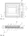
- FIG. 1A, FIG. 1B , FIG. 2, and FIG. 3 are for explaining a configuration of a hermetic package device according to Embodiment 1
- FIG. 1A is a plan view in which a lid wafer portion of the hermetic package device is see-through
- FIG. 1B is a cross-sectional view corresponding to the A-A line in FIG. 1A
- FIG. 2 is a partial cross-sectional view in which a region R1 in FIG. 1B is enlarged.
- FIG. 1A, FIG. 1B , FIG. 2, and FIG. 3 are for explaining a configuration of a hermetic package device according to Embodiment 1
- FIG. 1A is a plan view in which a lid wafer portion of the hermetic package device is see-through
- FIG. 1B is a cross-sectional view corresponding to the A-A line in FIG. 1A
- FIG. 2 is a partial cross-sectional view in which a region R1 in FIG. 1B is enlarged.
- FIG. 3 is a graphical representation of a relationship between a dimension of a positional shift at an intersection point with the lid wafer with respect to an intersection point with the device wafer on an outer surface of a potion in the sealing part facing an installation region of bonding pads and stresses applied to those intersection points.
- a part of a device wafer 1 protrudes relative to a lid wafer 2, and flat surfaces (mounting surface 1ff, opposed surface 2ff) are placed in parallel to face each other and are bonded by a sealing part 6.
- the sealing part 6 is formed of a first under-layer 61 patterned in a closed curve shape on the mounting surface 1ff of the device wafer 1, a second under-layer 62 patterned in a closed curve shape on the surface of the lid wafer 2 (opposed surface 2ff), and a sealing material layer 60 interposed between them. Both the first under-layer 61 and the second under-layer 62 are patterned in the closed curve shape (ring-shaped) and are sometimes referred to as sealing rings.
- the sealing material layer 60 is a solder material and has low wettability to the surface of the device wafer 1 (mounting surface 1ff) and the surface of the lid wafer 2 (opposed surface 2ff), making it difficult to bond the device wafer 1 and the lid wafer 2 as they are. Therefore, the first under-layer 61 and the second under-layer 62 are formed of a material with good wettability to the solder material and good adhesion to each wafer so as to function as an intermediate layer for bonding each wafer and the sealing material layer 60.
- a hermetically sealed space 100s surrounded by the device wafer 1, the lid wafer 2, and the sealing part 6 is maintained in a vacuum atmosphere by the sealing part 6 formed in this way.
- the sealing part 6 is formed with a thickness of about 50 to 150 ⁇ m, and in the present embodiment, it has a thickness of 100 ⁇ m.
- the inside of the hermetically sealed space 100s is in a vacuum atmosphere, it does not mean a complete vacuum, but only a degree of vacuum necessary to maintain the thermal insulation. If the pressure is lower than that of the outside air at least to an extent that it is a factor for the stress occurrence, the need to relieve the stress to be described later arises.
- an image sensing element 3 for infrared light In the region inside the sealing part 6 of the device wafer 1, that is, in the hermetically sealed space 100s, an image sensing element 3 for infrared light, a scanning circuit 4, and a readout circuit 5 each are arranged and maintained in a vacuum atmosphere with excellent thermal insulation, thereby enhancing the reliability as the infrared sensor.
- the MEMS and a semiconductor element that include the image sensing element 3, the scanning circuit 4, and the readout circuit 5 are collectively referred to as a semiconductor circuit 7.
- a plurality of bonding pads 8 (terminals) electrically connected to the image sensing element 3, the scanning circuit 4, and the readout circuit 5 via wiring (not shown) are arranged in a region of the device wafer 1 outside the sealing part 6 and in the part protruding relative to the lid wafer 2.
- a gas adsorbent (not shown) called a getter for maintaining the degree of vacuum is formed at a portion surrounded by the second under-layer 62.
- a recess may be formed to increase the vacuum volume.
- an anti-reflection coating called an AR coating may be formed on the outer surface of the lid wafer 2 (the surface opposite to the opposed surface 2ff) to improve the infrared transmittance.
- a width W61 of the first under-layer 61 formed on the device wafer 1 is set to be narrower than a width W62 of the second under-layer 62 formed on the lid wafer 2.
- the cross-sectional shape perpendicular to the extending direction of the sealing part 6 is an inverted trapezoid formed by connecting both ends of the first under-layer 61 and the second under-layer 62.
- the horizontal axis in FIG. 3 shows the dimension ⁇ P of the positional shift of an intersection point P2x with respect to an intersection point P1x in the portion facing the part of the device wafer 1 protruding relative to the lid wafer 2, the intersection point P2x being between an outer surface 6fx of the sealing part 6 and the surface of the lid wafer 2 (the opposed surface 2ff), the intersection point P1x being between the outer surface 6fx of the sealing part 6 and the surface of the device wafer 1 (the mounting surface 1ff).
- first under-layer 61 and the second under-layer 62 are arranged with their centers aligned in a plan view (when viewed from a distant position in the z-direction).
- the inverted trapezoid with a symmetrical cross section is formed and the dimension ⁇ P of the positional shift is half the difference between the width W61 of the first under-layer 61 formed on the device wafer 1 and the width W62 of the second under-layer 62 formed on the lid wafer 2.
- the vertical axis shows each of the stresses at the intersection point P1x and the intersection point P2x, which is normalized by the stress at the intersection point P1x when the dimension ⁇ P of the positional shift is zero.
- the first under-layer 61 and the second under-layer 62 are so-called nickel strikes having multilayer structures made of titanium (Ti) of 0.1 ⁇ m in thickness, copper (Cu) of 0.3 ⁇ m, and nickel (Ni) of 1 to 5 ⁇ m from the respective wafer sides.
- the thickness of the sealing part 6 including these is 100 ⁇ m
- the value of stress that occurs when a temperature change of - 100 degrees C is generated is used. Note that the thickness of the sealing part 6 of each test specimen was within the range of 90 ⁇ 20 ⁇ m.
- the test results obtained show that the stress at the intersection point P1x between the mounting surface 1ff of the device wafer 1 and the outer surface 6fx of the sealing part 6 decreases as the dimension ⁇ P of the positional shift increases from 0.
- the test results obtained show that the stress at the intersection point P2x between the opposed face 2ff of the lid wafer 2 and the outer face 6fx of the sealing part 6 increases, and when the dimension ⁇ P of the positional shift is larger than 40 ⁇ m, the stress ratio exceeds 1 and the stress at the intersection point P1x in the case of the dimension ⁇ P being zero is exceeded.
- the cross-sectional shape of the sealing part 6 inverted trapezoidal, the stress application direction in the vertical direction at the sealing part 6 inclines to the horizontal direction, and the stress concentration at the intersection point P1x is relieved.
- the dimension ⁇ P of the positional shift exceed 50 ⁇ m, a crack occurred in the lid wafer 2.
- the lid wafer 2 had no semiconductor circuit or wiring, and operated normally as the sensor.
- the dimension ⁇ P of the positional shift is suitable to be larger than 0 ⁇ m and within a range of 50 ⁇ m or less, and can be freely selected within that range.
- the dimension ⁇ P of the positional shift is kept within the range of 5 to 30 ⁇ m, the stress value at both the intersection point P1x and the intersection point P2x can be made lower than that of the intersection point P1x of the case when the malfunction occurs, and the hermetic package device 100 with higher reliability can be obtained.
- the preferable range of the set value of the dimension ⁇ P of the positional shift is from 5 to 30 ⁇ m when taking into account the dimensional error in mass production.
- the first under-layer 61 of the device wafer 1 and the second under-layer 62 of the lid wafer 2 in each embodiment of the present application each are formed by electrolytic Ni plating.
- the width W61 and the width W61 by electroplating are achieved using existing photolithography technology, and any desirable width can be selected by the pattern size of a photomask.
- the mounting surface of the device wafer or the opposed surface of the lid wafer is provided with a inclination, it is possible to relieve the stress by blunting the angle with the outer surface of the sealing part without forming the inverted trapezoid.
- a device wafer or a lid wafer prepared by special processing such as forming an inclination in the mounting surface or opposed surface, individual packaging is required, and thus it is unsuitable for mass production.
- the hermetic package device 100 of the present application can be cut out after packaging collectively without any special processing such as forming the inclination on either the mounting surface 1ff or the opposed surface 2ff. That is, by forming the sealing part 6 with the inverted trapezoidal cross section, the device wafer 1 can be prevented from cracking and the highly reliable hermetic package device 100 can be obtained without impairing mass production efficiency.
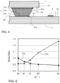
- FIG. 4 and FIG. 5 are for explaining a configuration of a hermetic package device according to Embodiment 2, and FIG. 4 is a partial cross-sectional view of the hermetic package device corresponding to FIG. 2 in Embodiment 1.
- FIG. 5 is a graphical representation of a relationship between an angle of the outer surface of the potion in the sealing part facing the installation region of the bonding pads with respect to the mounting surface of the device wafer and stresses applied to the intersection points of the outer surface with both wafers.
- Embodiment 2 As for the configuration of the hermetic package device according to Embodiment 2 other than the angle between the device wafer and the outer surface, the same configuration as that of Embodiment 1 can be applied, and the description of the similar part is omitted and FIG. 1A and FIG. 1B are referred to.
- the hermetic package device 100 according to Embodiment 2 in order to examine an effect of the inverted trapezoidal shape, several test specimens are fabricated using an angle ⁇ formed by the outer surface 6fx with respect to the mounting surface 1ff as a parameter, and results of the reliability test will be described.
- the horizontal axis in FIG. 5 shows the angle ⁇ formed by the outer surface 6fx of the sealing part 6 with respect to the mounting surface 1ff at the part where the device wafer 1 protrudes relative to the lid wafer 2.
- the vertical axis shows the stress at each of the intersection point P1x and intersection point P2x, normalized by the stress at the intersection point P1x when the angle ⁇ is 90 degrees.
- the first under-layer 61 and the second under-layer 62 have multilayer structures of titanium (Ti) of 0.1 ⁇ m in thickness, copper (Cu) 0.3 ⁇ m and nickel (Ni) 1 to 5 ⁇ m from the respective wafer sides, as in Embodiment 1.
- the test results obtained shows that the stress at the intersection point P1x between the device wafer 1 and the outer surface 6fx of the sealing part 6 decreases as the angle of the outer surface 6fx is changed to a side where the angle ⁇ decreases from 90 degrees, i.e., the angle at the portion of the sealing part 6 at the intersection point P1x is blunted.
- the test results obtained shows that the stress at the intersection point P2x between the lid wafer 2 and the outer surface 6fx of the sealing part 6 increases, and when the angle ⁇ is smaller than 60 degrees, the stress thereof exceeds that of the intersection point P1x in the case of the angle ⁇ being 90 degrees.
- the cross-sectional shape of the sealing part 6 inverted trapezoidal, the stress application direction in the vertical direction at the sealing part 6 inclines to the horizontal direction, and stress concentration at the intersection point P1x is relieved.
- the angle ⁇ is suitable to be in the range of 60 degrees or more and less than 90 degrees, and can be freely selected within that range.
- both the stress values at the portion of intersection point P1x and the intersection point P2x can be made lower than the stress value of the intersection point P1x in the case where the malfunction occurred, and a more reliable hermetic package device 100 can be obtained.
- the more favorable range of a set value of the angle ⁇ is 70 degrees or more and 85 degrees or less.
- the first under-layer 61 of the device wafer 1 and the second under-layer 62 of the lid wafer 2 in Embodiment 2 of the present application are respectively formed by electrolytic Ni plating.
- the width W61, the width W61, and the positional relationship thereof for defining the angle ⁇ are achieved using existing photolithography technology, and it is possible to set a desirable angle ⁇ by the pattern size of a photomask.
- lead-free solder is used for the sealing material layer 60 in the hermetic package device 100 of the present application, and a desirable thickness of the sealing part 6 (including the thickness of the first under-layer 61 and the second under-layer 62) can be obtained by adjusting the amount of lead-free solder for use. Therefore, by adjusting each of the widths W61, W62 and each of the positions of the first under-layer 61 and the second under-layer 62, and the thickness of the sealing part 6, a desirable angle ⁇ can be obtained.
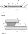
- FIG. 6 and FIG. 7 are for explaining a configuration of a hermetic package device according to Embodiment 3, FIG. 6 is a cross-sectional view of the hermetic package device corresponding to FIG. 1B in Embodiment 1, and FIG. 7 is a partial cross-sectional view in which a region R2 in FIG. 6 is enlarged.
- Embodiment 3 except for the setting of a portion to which the inclination of the sealing part of the hermetic package device according to Embodiment 3 is to be provided, the same configuration as that in Embodiment 1 or Embodiment 2 can be applied, and the description of the same part is omitted and FIG. 1A , FIG. 3 , and FIG. 5 are referred to.
- the outer surface 6fx only for the sealing part 6 in a region of the device wafer 1 where the bonding pads 8 are arranged is inclined with respect to the device wafer 1.
- no inclination is intentionally provided for both the outer surface 6fx and an inner surface 6fi, as with a typical sealing part.
- the inner surface 6fi is perpendicular to the device wafer 1, but the same stress relief effect as in Embodiment 1 and Embodiment 2 can be obtained in accordance with a setting range of the dimension ⁇ P of the positional shift, or the angle ⁇ formed with the mounting surface 1ff, which is caused by the inclination of the outer surface 6fx.
- the width W61 of the first under-layer 61 of the device wafer 1 can be made larger by inclining the outer surface 6fx larger than the inner surface 6fi within the setting range, as compared with the case where both surfaces are inclined equally. It is effective when there is no room to reduce the width W61 of the first under-layer 61 on the device wafer 1 or when the width W62 of the first under-layer 61 of the lid wafer 2 cannot be enlarged, due to layout constraint of the semiconductor circuit 7.
- the width W61 of the first under-layer 61 and the width W62 of the second under-layer 62 affect the hermeticity, and if they are too narrow, it may lead to deterioration of the hermeticity over time.
- a nearly vertical structure is to be adopted in which inclination is not intentionally provided as in the case of a typical sealing part.
- the inner surface 6fi is to be less inclined than the outer surface 6fx.
- FIG. 8 to FIG. 10 are for explaining a configuration of a hermetic package device according to Embodiment 4, FIG. 8 is a plan view in which a lid wafer portion of the hermetic package device is see-through, and FIG. 9 is a cross-sectional view corresponding to the B-B line in FIG. 8 .
- FIG. 10 is a cross-sectional view corresponding to the B-B line of FIG. 8 in a hermetic package device according to another example in Embodiment 4.
- the same configuration as that of Embodiment 1 to Embodiment 3 can be applied, and the explanation of the similar part is omitted, and FIG. 2 to FIG. 6 are referred to.
- the device wafer 1 protrudes relative to the lid wafer 2 on both sides in one direction (x-direction) of a plane (xy plane) parallel to the mounting surface 1ff, and bonding pads 8 are formed in each protruded region.
- the cross-sectional shape of the potions of the sealing part 6 facing the region where the bonding pads 8 are formed is such that, for example, the inner surface 6fi and the outer surface 6fx are uniformly inclined in order for the shape to be inverted trapezoid as in Embodiment 1 or Embodiment 2, as shown in FIG. 9 .
- the inner surface 6fi and the outer surface 6fx are uniformly inclined in order for the shape to be inverted trapezoid as in Embodiment 1 or Embodiment 2, as shown in FIG. 9 .
- FIG. 10 as in Embodiment 3 only the outer surface 6fx is inclined and the inner surface 6fi is not intentionally inclined.
- the same effect as in Embodiment 1 and Embodiment 2 or Embodiment 3 can be achieved by providing the inclination as shown in FIG. 9 and FIG. 10 on the outer surface 6fx of the sealing part 6 on the sides provided with the pads. That is, even in the case of the hermetic package device 100 in which the bonding pads 8 are arranged on two or more sides, the effect of relieving the stress can be obtained by providing the inclination on the outer surface 6fx without impairing mass production efficiency.
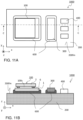
- FIG. 11A and FIG. 11B are for explaining a configuration of the device module according to Embodiment 5
- FIG. 11A is a plan view of the device module
- FIG. 11B is a cross-sectional view corresponding to the C-C line of FIG. 11A .
- the configuration of the hermetic package device is the same as that of any of Embodiment 1 to Embodiment 4, the description of the same part is omitted, and FIG. 1A and FIG. 1B , and FIG. 2 to FIG. 10 will be referred to.
- the device module 1000 according to Embodiment 5 has the hermetic package device 100, another semiconductor device 300, and electronic components 400 such as resistors and capacitors, which are mounted on a mounting surface 200fm of a circuit board 200. Then, components that are mounted are electrically connected by wire bonding or the like (not shown) to form the device module 1000.
- the hermetic package device 100 and the semiconductor device 300 are fixed to the circuit board 200 using a thermosetting adhesive 600.
- parts, a cover, etc. necessary for the device are provided, although not shown.
- the device module 1000 according to Embodiment 5 is equipped with the hermetic package device 100 described in any of Embodiment 1 to Embodiment 4 to be robust against vibration and shock.
- the hermetic package device 100 that functions as an infrared sensor, it is possible to obtain a highly reliable infrared sensor that is robust against vibration and shock, and prevents cracking of the device wafer.
- the example of forming the first under-layer 61 and the second under-layer 62 using the electrolytic Ni plating have been described, but the electrolytic plating is not a limitation, and for example, electroless plating, a sputtering method, or a metal organic chemical vapor deposition (MO-CVD) method can be adopted as the forming method.
- the method of adjusting the width W61 of the first under-layer 61 and the width W62 of the second under-layer 62 using photolithography has been described.
- the photolithography is not a limitation, and a method of printing, inkjet, or mask sputtering can be employed.
- the example of setting the dimension ⁇ P of the positional shift, or the angle of inclination ⁇ by the width W61 of the first under-layer 61 and the width W62 of the second under-layer 62 has been shown, but it is not a limitation.
- the cross-sectional shape (dimension ⁇ P of positional shift, angle ⁇ ) of the sealing part 6 may be set by forming a layer made of a non-affinity material outside the regions where the first under-layer 61 and the second under-layer 62 were assumed.
- the sealing material layer 60 may be selectively adhered to the mounting surface 1ff and the opposed surface 2ff by making the surface roughness of the regions where the first under-layer 61 and the second under-layer 62 were assumed to be formed larger than other portions.
- the material of the solder is not limited to this, a desirable material can be selected, and the material of the under-layers can be changed accordingly.
- the lead-free solder is preferred to high-temperature solder or AuSn, because of its high environmental impact and a high price.
- the material of the adhesive 600 has been described for fixing the hermetic package device 100 and the semiconductor device 300, the material of the adhesive is not limited to this, and a desirable material can be selected. However, since a UV-cured type adhesive shrinks more during curing, the thermosetting type adhesive is more suitable.
- the hermetic package device 100 includes the device wafer 1 in which the semiconductor circuit 7 and the terminals (bonding pads 8) for electrical connection to an outside are provided on the mounting surface 1ff, the lid wafer 2 arranged to be opposed to the mounting surface 1ff of the device wafer 1, and the sealing part 6 that surrounds the installation region of the semiconductor circuit 7 in the mounting surface 1ff, is interposed between the device wafer 1 and the lid wafer 2, and forms the hermetically sealed space 100s in a vacuum atmosphere to house the semiconductor circuit 7 between the device wafer 1 and the lid wafer 2.
- the second installation region in the mounting surface 1ff in which the terminals (bonding pads 8) are provided protrudes relative to the lid wafer 2, and the outer surface 6fx of the portion in the sealing part 6 facing the second installation region is formed to be inclined such that a position thereon approaches the second installation region when getting closer from the device wafer 1 toward the lid wafer 2. Because of the above, it is possible to prevent the device wafer 1 from cracking and obtain a highly reliable hermetic package device 100 without impairing mass production efficiency.
- the sealing part 6 is formed of the first under-layer 61 patterned on the mounting surface 1ff of the device wafer 1, the second under-layer 62 patterned in the lid wafer 2 on the opposed surface 2ff of the mounting surface 1ff, and the sealing material layer 60 for filling between the first under-layer 61 and the second under-layer 62, and when, in the portion in the sealing part 6 facing the second installation region, the end of the second under-layer 62 on the side near the second installation region (intersection point P2x) has a positional shift toward the second installation region with respect to the end of the first under-layer 61 on the side near the second installation region (intersection point P1x), the above-mentioned inclination can be accurately formed.
- the dimension ⁇ P of the positional shift is within the range of 5 to 30 ⁇ m, cracking of the lid wafer 2 is also prevented and reliability is enhanced.
- the cross-sectional shape of the sealing part 6 can be set reliably.
- the angle ⁇ formed by the outer surface 6fx with respect to the mounting surface 1ff is within the range of 60 degrees or more and less than 90 degrees, cracking of the device wafer 1 can be reliably prevented.
- the angle ⁇ formed by the outer surface 6fx with respect to the mounting surface 1ff is within the range of 70 degrees or more and 85 degrees or less, cracking of the lid wafer 2 is also prevented and the reliability is enhanced.
- the sealing width is secured to the extent possible and a highly reliable hermetic package device 100 can be obtained.
- the hermetic package device 100 described above is configured such that the image sensing element 3 for infrared light is used for the semiconductor circuit 7 and an infrared transmission material is used for the lid wafer 2 so as to function as an infrared sensor, a highly reliable infrared sensor can be obtained.
- a highly reliable device module 1000 can be obtained because the module is configured to include the circuit board 200, the above-described hermetic package device 100 mounted on the circuit board 200, and electronic components (semiconductor device 300, electronic components 400) mounted on the circuit board 200 and electrically connected to the terminals (bonding pads 8).
Landscapes
- Engineering & Computer Science (AREA)
- Microelectronics & Electronic Packaging (AREA)
- Computer Hardware Design (AREA)
- Solid State Image Pick-Up Elements (AREA)
- Micromachines (AREA)
Abstract
Description
- The present application relates to a hermetic package device and a device module.
- Micro Electro Mechanical Systems (MEMS) devices, which are devices in which sensors, actuators, etc. are integrated on a silicon substrate, etc. by microfabrication technology, have been put into practical use. Examples of MEMS devices include an infrared sensor, a gyro sensor, an accelerometer, and the like.
- Among infrared sensors, an uncooled infrared sensor converts incoming infrared light into heat, as referred to as a thermal sensor. Therefore, the sensor (image sensing element) has a configuration in which a temperature change of a target object is read out as a change of an electric signal, and has an adiabatic structure that is thermally isolated from a base material in order to increase the detection sensitivity. Specifically, the infrared sensor is disposed in a hermetically sealed vacuum space, that is, inside a vacuum package, to enhance the thermal insulation. In this case, it is known that a material used as a lid of the vacuum package is ZnS or silicon containing low oxygen with high infrared transmittance, or an anti-reflection coating (AR coating) is formed on the material.
- On the other hand, as a method of manufacturing a vacuum package, a wafer-level package has been proposed in which a wafer on which MEMS devices are manufactured and a lid wafer facing the device wafer are bonded in a vacuum atmosphere to form a plurality of vacuum packages (Refer to, for example, Patent Document 1).
- Patent Document 1:
Japanese Patent Application Laid-Open No.2003-531475 FIG. 1 to FIG. 4 ) - A device formed using the wafer-level package inevitably has a structure in which bonding pads for electrical connection provided on the device wafer are exposed from the lid wafer, and the part for the bonding in the device wafer protrudes relative to the lid wafer. In such a structure where one side thereof protrudes, there have been problems in which stress concentration occurs in a portion where the sealing part on the protruding side of the device wafer is in contact with the device wafer, causing cracks in the device wafer and malfunction of the device due to circuit breakage, wiring disconnection, etc.
- The present application discloses a technology to solve the above problems, and an object thereof is to prevent device wafer cracking and obtain a highly reliable hermetic package device.
- A hermetic package device disclosed in the present application includes a device wafer in which a semiconductor circuit and terminals for electrical connection to an outside are provided on a mounting surface, a lid wafer arranged to be opposed to the mounting surface of the device wafer, and a sealing part that surrounds an installation region of the semiconductor circuit in the mounting surface, is interposed between the device wafer and the lid wafer, and forms a hermetically sealed space in a vacuum atmosphere to house the semiconductor circuit between the device wafer and the lid wafer. A second installation region in the mounting surface in which the terminals are provided protrudes relative to the lid wafer, and an outer surface of a portion in the sealing part facing the second installation region is inclined such that a position thereon approaches the second installation region when getting closer from the device wafer toward the lid wafer.
- According to the hermetic package device or device module disclosed in the present application, the stress at the portion where the sealing part is in contact with the device wafer can be relieved, so that cracking of the device wafer can be prevented and a highly reliable hermetic package device can be obtained.
-
-
FIG. 1A and FIG. 1B are a plan view and a cross-sectional view, respectively, of a hermetic package device according toEmbodiment 1. -
FIG. 2 is an enlarged partial cross-sectional view of a part of the hermetic package device according toEmbodiment 1. -
FIG. 3 is a graphical representation of a relationship between a dimension of a positional shift at an intersection point with a lid wafer with respect to an intersection point with a device wafer on an outer surface of a sealing part and stresses applied to those intersection points, in the hermetic package device. -
FIG. 4 is an enlarged partial cross-sectional view of a part of a hermetic package device according toEmbodiment 2. -
FIG. 5 is a graphical representation of a relationship between an angle formed by the outer surface of the sealing part with respect to the mounting surface of the device wafer and stresses applied to a position of an edge in a seal ring on the lid wafer side and a position of an edge of a seal ring on the device wafer side, in the hermetic package device. -
FIG. 6 is a cross-sectional view of a hermetic package device according toEmbodiment 3. -
FIG. 7 is an enlarged partial cross-sectional view of a part of the hermetic package device according toEmbodiment 3. -
FIG. 8 is a partially transparent plan view of a hermetic package device according to Embodiment 4. -
FIG. 9 is a cross-sectional view of the hermetic package device according to Embodiment 4. -
FIG. 10 is a cross-sectional view of a hermetic package device according to another example inEmbodiment 4. -
FIG. 11A and FIG. 11B are a plan view and a cross-sectional view, respectively, of a device module according to Embodiment 11. - Hereinafter, hermetic package devices according to embodiments of the present application are described on the basis of the drawings. Note that, in the following drawings, the same or corresponding parts will be given the same reference number and the description thereof will not be repeated.
-
FIG. 1A, FIG. 1B ,FIG. 2, and FIG. 3 are for explaining a configuration of a hermetic package device according toEmbodiment 1,FIG. 1A is a plan view in which a lid wafer portion of the hermetic package device is see-through,FIG. 1B is a cross-sectional view corresponding to the A-A line inFIG. 1A , andFIG. 2 is a partial cross-sectional view in which a region R1 inFIG. 1B is enlarged.FIG. 3 is a graphical representation of a relationship between a dimension of a positional shift at an intersection point with the lid wafer with respect to an intersection point with the device wafer on an outer surface of a potion in the sealing part facing an installation region of bonding pads and stresses applied to those intersection points. - First, a basic configuration of the hermetic package device will be is described. In the
hermetic package device 100, as shown inFIG. 1A and FIG. 1B , a part of a device wafer 1 protrudes relative to alid wafer 2, and flat surfaces (mounting surface 1ff, opposed surface 2ff) are placed in parallel to face each other and are bonded by a sealingpart 6. The sealingpart 6 is formed of a first under-layer 61 patterned in a closed curve shape on the mounting surface 1ff of thedevice wafer 1, a second under-layer 62 patterned in a closed curve shape on the surface of the lid wafer 2 (opposed surface 2ff), and a sealingmaterial layer 60 interposed between them. Both the first under-layer 61 and the second under-layer 62 are patterned in the closed curve shape (ring-shaped) and are sometimes referred to as sealing rings. - The sealing
material layer 60 is a solder material and has low wettability to the surface of the device wafer 1 (mounting surface 1ff) and the surface of the lid wafer 2 (opposed surface 2ff), making it difficult to bond thedevice wafer 1 and thelid wafer 2 as they are. Therefore, the first under-layer 61 and the second under-layer 62 are formed of a material with good wettability to the solder material and good adhesion to each wafer so as to function as an intermediate layer for bonding each wafer and the sealingmaterial layer 60. - A hermetically sealed
space 100s surrounded by the device wafer 1, the lid wafer 2, and the sealingpart 6 is maintained in a vacuum atmosphere by the sealingpart 6 formed in this way. In order to secure the vacuum volume, the sealingpart 6 is formed with a thickness of about 50 to 150 µm, and in the present embodiment, it has a thickness of 100 µm. Although the inside of the hermetically sealedspace 100s is in a vacuum atmosphere, it does not mean a complete vacuum, but only a degree of vacuum necessary to maintain the thermal insulation. If the pressure is lower than that of the outside air at least to an extent that it is a factor for the stress occurrence, the need to relieve the stress to be described later arises. - In the region inside the sealing
part 6 of the device wafer 1, that is, in the hermetically sealedspace 100s, animage sensing element 3 for infrared light, ascanning circuit 4, and areadout circuit 5 each are arranged and maintained in a vacuum atmosphere with excellent thermal insulation, thereby enhancing the reliability as the infrared sensor. Note that the MEMS and a semiconductor element that include theimage sensing element 3, thescanning circuit 4, and thereadout circuit 5 are collectively referred to as asemiconductor circuit 7. In addition, a plurality of bonding pads 8 (terminals) electrically connected to theimage sensing element 3, thescanning circuit 4, and thereadout circuit 5 via wiring (not shown) are arranged in a region of the device wafer 1 outside the sealingpart 6 and in the part protruding relative to thelid wafer 2. - On the other hand, on the
lid wafer 2, a gas adsorbent (not shown) called a getter for maintaining the degree of vacuum is formed at a portion surrounded by the second under-layer 62. In addition, a recess may be formed to increase the vacuum volume. Further, an anti-reflection coating called an AR coating may be formed on the outer surface of the lid wafer 2 (the surface opposite to the opposed surface 2ff) to improve the infrared transmittance. When thebonding pads 8 of thehermetic package device 100 thus configured are electrically connected to a circuit board (not shown) or the like, with wires or the like, an device module 1000 (FIG. 11A, FIG. 11B ) to be described later functions. - On the basis of the above configuration, a characteristic configuration of the
hermetic package device 100 in the present application will be described. In thehermetic package device 100 of the present application, as shown inFIG. 2 , a width W61 of the first under-layer 61 formed on thedevice wafer 1 is set to be narrower than a width W62 of the second under-layer 62 formed on thelid wafer 2. InEmbodiment 1, at least in a portion facing the part of thedevice wafer 1 protruding relative to thelid wafer 2, the cross-sectional shape perpendicular to the extending direction of the sealingpart 6 is an inverted trapezoid formed by connecting both ends of the first under-layer 61 and the second under-layer 62. - Next, in order to verify an effect of the inverted trapezoid, several kinds of test specimens were prepared using the dimension ΔP of the positional shift as a parameter, and results of reliability tests will be explained. The horizontal axis in
FIG. 3 shows the dimension ΔP of the positional shift of an intersection point P2x with respect to an intersection point P1x in the portion facing the part of thedevice wafer 1 protruding relative to thelid wafer 2, the intersection point P2x being between an outer surface 6fx of the sealingpart 6 and the surface of the lid wafer 2 (the opposed surface 2ff), the intersection point P1x being between the outer surface 6fx of the sealingpart 6 and the surface of the device wafer 1 (the mounting surface 1ff). It is assumed that the first under-layer 61 and the second under-layer 62 are arranged with their centers aligned in a plan view (when viewed from a distant position in the z-direction). In other words, it is assumed that the inverted trapezoid with a symmetrical cross section is formed and the dimension ΔP of the positional shift is half the difference between the width W61 of the first under-layer 61 formed on thedevice wafer 1 and the width W62 of the second under-layer 62 formed on thelid wafer 2. - Further, the vertical axis shows each of the stresses at the intersection point P1x and the intersection point P2x, which is normalized by the stress at the intersection point P1x when the dimension ΔP of the positional shift is zero. Here, the first under-
layer 61 and the second under-layer 62 are so-called nickel strikes having multilayer structures made of titanium (Ti) of 0.1 µm in thickness, copper (Cu) of 0.3 µm, and nickel (Ni) of 1 to 5µm from the respective wafer sides. Then, assuming that the thickness of the sealingpart 6 including these is 100 µm, the value of stress that occurs when a temperature change of - 100 degrees C is generated is used. Note that the thickness of the sealingpart 6 of each test specimen was within the range of 90 ± 20 µm. - As shown in
FIG. 3 , the test results obtained show that the stress at the intersection point P1x between the mounting surface 1ff of thedevice wafer 1 and the outer surface 6fx of the sealingpart 6 decreases as the dimension ΔP of the positional shift increases from 0. On the other hand, the test results obtained show that the stress at the intersection point P2x between the opposed face 2ff of thelid wafer 2 and the outer face 6fx of the sealingpart 6 increases, and when the dimension ΔP of the positional shift is larger than 40 µm, the stress ratio exceeds 1 and the stress at the intersection point P1x in the case of the dimension ΔP being zero is exceeded. In other words, by making the cross-sectional shape of the sealingpart 6 inverted trapezoidal, the stress application direction in the vertical direction at the sealingpart 6 inclines to the horizontal direction, and the stress concentration at the intersection point P1x is relieved. - In the case of a test specimen in which the dimension ΔP of the positional shift was 0, that is, an under-layer of the same width (W61 = W62) was formed on each of the
device wafer 1 and thelid wafer 2, a crack occurred in a portion at the intersection point P1x between thedevice wafer 1 and the outer surface 6fx, resulting in malfunction of the sensor. In contrast, no malfunction occurred in test specimens whose dimension ΔP of the positional shift was increased from 0 to 50 µm. - However, when the dimension ΔP of the positional shift exceeded 50 µm, a crack occurred in the
lid wafer 2. Thelid wafer 2 had no semiconductor circuit or wiring, and operated normally as the sensor. However, since there is a concern that a foreign object adheres to thedevice wafer 1 when the crack occur, the dimension ΔP of the positional shift is suitable to be larger than 0 µm and within a range of 50 µm or less, and can be freely selected within that range. - If the dimension ΔP of the positional shift is kept within the range of 5 to 30 µm, the stress value at both the intersection point P1x and the intersection point P2x can be made lower than that of the intersection point P1x of the case when the malfunction occurs, and the
hermetic package device 100 with higher reliability can be obtained. In other words, the preferable range of the set value of the dimension ΔP of the positional shift is from 5 to 30 µm when taking into account the dimensional error in mass production. - The first under-
layer 61 of thedevice wafer 1 and the second under-layer 62 of thelid wafer 2 in each embodiment of the present application each are formed by electrolytic Ni plating. The width W61 and the width W61 by electroplating are achieved using existing photolithography technology, and any desirable width can be selected by the pattern size of a photomask. - For example, if the mounting surface of the device wafer or the opposed surface of the lid wafer is provided with a inclination, it is possible to relieve the stress by blunting the angle with the outer surface of the sealing part without forming the inverted trapezoid. However, in such a case, using a device wafer or a lid wafer prepared by special processing such as forming an inclination in the mounting surface or opposed surface, individual packaging is required, and thus it is unsuitable for mass production.
- In contrast, the
hermetic package device 100 of the present application can be cut out after packaging collectively without any special processing such as forming the inclination on either the mounting surface 1ff or the opposed surface 2ff. That is, by forming the sealingpart 6 with the inverted trapezoidal cross section, thedevice wafer 1 can be prevented from cracking and the highly reliablehermetic package device 100 can be obtained without impairing mass production efficiency. - In
Embodiment 1 described above, an example of relieving the stress by adjusting the range of the dimension of the positional shift was described. InEmbodiment 2, an example of relieving the stress by adjusting an inclination of the outer surface of the sealing part will be described.FIG. 4 and FIG. 5 are for explaining a configuration of a hermetic package device according toEmbodiment 2, andFIG. 4 is a partial cross-sectional view of the hermetic package device corresponding toFIG. 2 inEmbodiment 1.FIG. 5 is a graphical representation of a relationship between an angle of the outer surface of the potion in the sealing part facing the installation region of the bonding pads with respect to the mounting surface of the device wafer and stresses applied to the intersection points of the outer surface with both wafers. - As for the configuration of the hermetic package device according to
Embodiment 2 other than the angle between the device wafer and the outer surface, the same configuration as that ofEmbodiment 1 can be applied, and the description of the similar part is omitted andFIG. 1A and FIG. 1B are referred to. - In the
hermetic package device 100 according toEmbodiment 2, as shown inFIG. 4 , in order to examine an effect of the inverted trapezoidal shape, several test specimens are fabricated using an angle θ formed by the outer surface 6fx with respect to the mounting surface 1ff as a parameter, and results of the reliability test will be described. The horizontal axis inFIG. 5 shows the angle θ formed by the outer surface 6fx of the sealingpart 6 with respect to the mounting surface 1ff at the part where thedevice wafer 1 protrudes relative to thelid wafer 2. - The vertical axis shows the stress at each of the intersection point P1x and intersection point P2x, normalized by the stress at the intersection point P1x when the angle θ is 90 degrees. Here, the first under-
layer 61 and the second under-layer 62 have multilayer structures of titanium (Ti) of 0.1 µm in thickness, copper (Cu) 0.3 µm and nickel (Ni) 1 to 5 µm from the respective wafer sides, as inEmbodiment 1. - As shown in
FIG. 4 , the test results obtained shows that the stress at the intersection point P1x between thedevice wafer 1 and the outer surface 6fx of the sealingpart 6 decreases as the angle of the outer surface 6fx is changed to a side where the angle θ decreases from 90 degrees, i.e., the angle at the portion of the sealingpart 6 at the intersection point P1x is blunted. On the other hand, the test results obtained shows that the stress at the intersection point P2x between thelid wafer 2 and the outer surface 6fx of the sealingpart 6 increases, and when the angle θ is smaller than 60 degrees, the stress thereof exceeds that of the intersection point P1x in the case of the angle θ being 90 degrees. In other words, by making the cross-sectional shape of the sealingpart 6 inverted trapezoidal, the stress application direction in the vertical direction at the sealingpart 6 inclines to the horizontal direction, and stress concentration at the intersection point P1x is relieved. - In the case of a test specimen with an angle θ of 90 degrees, that is, with a rectangular cross section of the sealing
part 6, a crack occurred at the portion of the intersection point P1x between thedevice wafer 1 and the outer surface 6fx, resulting in malfunction of the sensor. In contrast, no malfunction occurred in the test specimens with the angle θ decreased from 90 degrees. - However, when the angle θ was close to 40 degrees, a crack occurred in the
lid wafer 2. Thelid wafer 2 had no semiconductor circuit or wiring, and operated normally as a sensor. However, since there is a concern that a foreign object adheres to thedevice wafer 1 when cracks occur, the angle θ is suitable to be in the range of 60 degrees or more and less than 90 degrees, and can be freely selected within that range. - If the angle θ is kept within the range of 70 degrees or more and 85 degrees or less, both the stress values at the portion of intersection point P1x and the intersection point P2x can be made lower than the stress value of the intersection point P1x in the case where the malfunction occurred, and a more reliable
hermetic package device 100 can be obtained. In other words, if dimensional errors and other factors at the time of mass production are also taken into consideration, the more favorable range of a set value of the angle θ is 70 degrees or more and 85 degrees or less. - The above results were similar to the case where the thickness of the sealing
part 6 was changed or when the center positions of the first under-layer 61 and the second under-layer 62 were shifted. That is, by setting the angle θ of the outer surface 6fx with respect to the mounting surface 1ff within the range described above, it is possible to prevent thedevice wafer 1 from cracking and achieve the effect of obtaining a highly reliablehermetic package device 100 without impairing mass production efficiency. - The first under-
layer 61 of thedevice wafer 1 and the second under-layer 62 of thelid wafer 2 inEmbodiment 2 of the present application are respectively formed by electrolytic Ni plating. The width W61, the width W61, and the positional relationship thereof for defining the angle θ are achieved using existing photolithography technology, and it is possible to set a desirable angle θ by the pattern size of a photomask. - In addition, lead-free solder is used for the sealing
material layer 60 in thehermetic package device 100 of the present application, and a desirable thickness of the sealing part 6 (including the thickness of the first under-layer 61 and the second under-layer 62) can be obtained by adjusting the amount of lead-free solder for use. Therefore, by adjusting each of the widths W61, W62 and each of the positions of the first under-layer 61 and the second under-layer 62, and the thickness of the sealingpart 6, a desirable angle θ can be obtained. - In
Embodiment 1 orEmbodiment 2 described above, the example of making the cross-sectional shape of the sealing part symmetrical and inverted trapezoidal has been described, but this is not a limitation. InEmbodiment 3, an example will be described in which the inclination is provided only on the outer surface where the stress relief is necessary, and the inner surface is not intentionally inclined or is less inclined than the outer surface.FIG. 6 and FIG. 7 are for explaining a configuration of a hermetic package device according toEmbodiment 3,FIG. 6 is a cross-sectional view of the hermetic package device corresponding toFIG. 1B inEmbodiment 1, andFIG. 7 is a partial cross-sectional view in which a region R2 inFIG. 6 is enlarged. - Note that, except for the setting of a portion to which the inclination of the sealing part of the hermetic package device according to
Embodiment 3 is to be provided, the same configuration as that inEmbodiment 1 orEmbodiment 2 can be applied, and the description of the same part is omitted andFIG. 1A ,FIG. 3 , andFIG. 5 are referred to. - As shown in
FIG. 6 and FIG. 7 , in thehermetic package device 100 according toEmbodiment 3, the outer surface 6fx only for the sealingpart 6 in a region of thedevice wafer 1 where thebonding pads 8 are arranged is inclined with respect to thedevice wafer 1. In the sealingpart 6, in regions other than in the region where thebonding pads 8 are arranged, no inclination is intentionally provided for both the outer surface 6fx and an inner surface 6fi, as with a typical sealing part. In the region where thebonding pads 8 are arranged, the inner surface 6fi is perpendicular to thedevice wafer 1, but the same stress relief effect as inEmbodiment 1 andEmbodiment 2 can be obtained in accordance with a setting range of the dimension ΔP of the positional shift, or the angle θ formed with the mounting surface 1ff, which is caused by the inclination of the outer surface 6fx. - Furthermore, in the region where the
bonding pads 8 are arranged, the width W61 of the first under-layer 61 of thedevice wafer 1 can be made larger by inclining the outer surface 6fx larger than the inner surface 6fi within the setting range, as compared with the case where both surfaces are inclined equally. It is effective when there is no room to reduce the width W61 of the first under-layer 61 on thedevice wafer 1 or when the width W62 of the first under-layer 61 of thelid wafer 2 cannot be enlarged, due to layout constraint of thesemiconductor circuit 7. - The width W61 of the first under-
layer 61 and the width W62 of the second under-layer 62 affect the hermeticity, and if they are too narrow, it may lead to deterioration of the hermeticity over time. However, for the portions where the device operation is not affected by a crack caused by the stress concentration, a nearly vertical structure is to be adopted in which inclination is not intentionally provided as in the case of a typical sealing part. Or, the inner surface 6fi is to be less inclined than the outer surface 6fx. By doing so, thehermetic package device 100 with high hermeticity and reliable device operation can be obtained without impairing mass production efficiency. - In
Embodiment 1 toEmbodiment 3 described above, the case where the bonding pads are provided on one side of the hermetic package device was described, but it is not a limitation. A case in which the bonding pads are provided on two or more sides of a hermetic package device will be described inEmbodiment 4.FIG. 8 to FIG. 10 are for explaining a configuration of a hermetic package device according toEmbodiment 4,FIG. 8 is a plan view in which a lid wafer portion of the hermetic package device is see-through, andFIG. 9 is a cross-sectional view corresponding to the B-B line inFIG. 8 . - And,
FIG. 10 is a cross-sectional view corresponding to the B-B line ofFIG. 8 in a hermetic package device according to another example inEmbodiment 4. - In the hermetic package device according to
Embodiment 4, as for the configuration except for the arrangement of the bonding pads and the setting of portions in relation to the arrangement, to which the inclination of the sealing part is to be provided, the same configuration as that ofEmbodiment 1 toEmbodiment 3 can be applied, and the explanation of the similar part is omitted, andFIG. 2 to FIG. 6 are referred to. - In the
hermetic package device 100 according toEmbodiment 4, as shown inFIG. 8 , thedevice wafer 1 protrudes relative to thelid wafer 2 on both sides in one direction (x-direction) of a plane (xy plane) parallel to the mounting surface 1ff, andbonding pads 8 are formed in each protruded region. - The cross-sectional shape of the potions of the sealing
part 6 facing the region where thebonding pads 8 are formed is such that, for example, the inner surface 6fi and the outer surface 6fx are uniformly inclined in order for the shape to be inverted trapezoid as inEmbodiment 1 orEmbodiment 2, as shown inFIG. 9 . Alternatively, as another example, as shown inFIG. 10 , as inEmbodiment 3, only the outer surface 6fx is inclined and the inner surface 6fi is not intentionally inclined. - Even when the
bonding pads 8 are provided on multiple sides of thedevice wafer 1, the same effect as inEmbodiment 1 andEmbodiment 2 orEmbodiment 3 can be achieved by providing the inclination as shown inFIG. 9 andFIG. 10 on the outer surface 6fx of the sealingpart 6 on the sides provided with the pads. That is, even in the case of thehermetic package device 100 in which thebonding pads 8 are arranged on two or more sides, the effect of relieving the stress can be obtained by providing the inclination on the outer surface 6fx without impairing mass production efficiency. - In
Embodiment 5, a device module will be described in which the hermetic package device described above inEmbodiment 1 toEmbodiment 4 is mounted on a circuit board together with other electronic components.FIG. 11A and FIG. 11B are for explaining a configuration of the device module according toEmbodiment 5,FIG. 11A is a plan view of the device module, andFIG. 11B is a cross-sectional view corresponding to the C-C line ofFIG. 11A . Note that the configuration of the hermetic package device is the same as that of any ofEmbodiment 1 toEmbodiment 4, the description of the same part is omitted, andFIG. 1A and FIG. 1B , andFIG. 2 to FIG. 10 will be referred to. - As shown in
FIG. 11A and FIG. 11B , thedevice module 1000 according toEmbodiment 5 has thehermetic package device 100, anothersemiconductor device 300, andelectronic components 400 such as resistors and capacitors, which are mounted on a mounting surface 200fm of acircuit board 200. Then, components that are mounted are electrically connected by wire bonding or the like (not shown) to form thedevice module 1000. InEmbodiment 5, thehermetic package device 100 and thesemiconductor device 300 are fixed to thecircuit board 200 using athermosetting adhesive 600. In addition, parts, a cover, etc. necessary for the device are provided, although not shown. - The
device module 1000 according toEmbodiment 5 is equipped with thehermetic package device 100 described in any ofEmbodiment 1 toEmbodiment 4 to be robust against vibration and shock. For example, when using thehermetic package device 100 that functions as an infrared sensor, it is possible to obtain a highly reliable infrared sensor that is robust against vibration and shock, and prevents cracking of the device wafer. - Note that, although various exemplary embodiments and examples are described in the present application, various features, aspects, and functions described in one or more embodiments are not limited to the application exemplified in a particular embodiment and can be applicable alone or in their various combinations to each embodiment. Accordingly, countless variations that are not illustrated are envisaged within the scope of the art disclosed herein. For example, the case where at least one component is modified, added or omitted, and the case where at least one component is extracted and combined with a component in another embodiment disclosed are included.
- The example of forming the first under-
layer 61 and the second under-layer 62 using the electrolytic Ni plating have been described, but the electrolytic plating is not a limitation, and for example, electroless plating, a sputtering method, or a metal organic chemical vapor deposition (MO-CVD) method can be adopted as the forming method. In addition, the method of adjusting the width W61 of the first under-layer 61 and the width W62 of the second under-layer 62 using photolithography has been described. However, the photolithography is not a limitation, and a method of printing, inkjet, or mask sputtering can be employed. - Further, the example of setting the dimension ΔP of the positional shift, or the angle of inclination θ by the width W61 of the first under-
layer 61 and the width W62 of the second under-layer 62 has been shown, but it is not a limitation. For example, if the mounting surface 1ff and the opposed surface 2ff themselves have affinity with the material constituting the sealingmaterial layer 60, the cross-sectional shape (dimension ΔP of positional shift, angle θ) of the sealingpart 6 may be set by forming a layer made of a non-affinity material outside the regions where the first under-layer 61 and the second under-layer 62 were assumed. Alternatively, the sealingmaterial layer 60 may be selectively adhered to the mounting surface 1ff and the opposed surface 2ff by making the surface roughness of the regions where the first under-layer 61 and the second under-layer 62 were assumed to be formed larger than other portions. - Furthermore, although the example of using lead-free solder for the sealing
material layer 60 has been described, the material of the solder is not limited to this, a desirable material can be selected, and the material of the under-layers can be changed accordingly. However, the lead-free solder is preferred to high-temperature solder or AuSn, because of its high environmental impact and a high price. In addition, although the example using thethermosetting adhesive 600 has been described for fixing thehermetic package device 100 and thesemiconductor device 300, the material of the adhesive is not limited to this, and a desirable material can be selected. However, since a UV-cured type adhesive shrinks more during curing, the thermosetting type adhesive is more suitable. - As described above, the
hermetic package device 100 according to the present application includes thedevice wafer 1 in which thesemiconductor circuit 7 and the terminals (bonding pads 8) for electrical connection to an outside are provided on the mounting surface 1ff, thelid wafer 2 arranged to be opposed to the mounting surface 1ff of thedevice wafer 1, and the sealingpart 6 that surrounds the installation region of thesemiconductor circuit 7 in the mounting surface 1ff, is interposed between thedevice wafer 1 and thelid wafer 2, and forms the hermetically sealedspace 100s in a vacuum atmosphere to house thesemiconductor circuit 7 between thedevice wafer 1 and thelid wafer 2. The second installation region in the mounting surface 1ff in which the terminals (bonding pads 8) are provided protrudes relative to thelid wafer 2, and the outer surface 6fx of the portion in the sealingpart 6 facing the second installation region is formed to be inclined such that a position thereon approaches the second installation region when getting closer from thedevice wafer 1 toward thelid wafer 2. Because of the above, it is possible to prevent thedevice wafer 1 from cracking and obtain a highly reliablehermetic package device 100 without impairing mass production efficiency. - In particular, when the sealing
part 6 is formed of the first under-layer 61 patterned on the mounting surface 1ff of thedevice wafer 1, the second under-layer 62 patterned in thelid wafer 2 on the opposed surface 2ff of the mounting surface 1ff, and the sealingmaterial layer 60 for filling between the first under-layer 61 and the second under-layer 62, and when, in the portion in the sealingpart 6 facing the second installation region, the end of the second under-layer 62 on the side near the second installation region (intersection point P2x) has a positional shift toward the second installation region with respect to the end of the first under-layer 61 on the side near the second installation region (intersection point P1x), the above-mentioned inclination can be accurately formed. - In this case, if the dimension ΔP of the positional shift, is within the range of 50 µm or less, cracking of the
device wafer 1 can be reliably prevented. - More preferably, if the dimension ΔP of the positional shift is within the range of 5 to 30 µm, cracking of the
lid wafer 2 is also prevented and reliability is enhanced. - In addition, if lead-free solder is used for the sealing
material layer 60 and nickel is used for the first under-layers 61 and the second under-layers 62, the cross-sectional shape of the sealingpart 6 can be set reliably. - Alternatively, if the angle θ formed by the outer surface 6fx with respect to the mounting surface 1ff is within the range of 60 degrees or more and less than 90 degrees, cracking of the
device wafer 1 can be reliably prevented. - More preferably, if the angle θ formed by the outer surface 6fx with respect to the mounting surface 1ff is within the range of 70 degrees or more and 85 degrees or less, cracking of the
lid wafer 2 is also prevented and the reliability is enhanced. - When the inner surface 6fi of the portion in the sealing
part 6 provided with the inclination in the outer surface 6fx is formed to be inclined at an angle gentler than the outer surface 6fx in the opposite direction with respect to the outer surface 6fx, or is upright to the mounting surface 1ff, the sealing width is secured to the extent possible and a highly reliablehermetic package device 100 can be obtained. - When the
hermetic package device 100 described above is configured such that theimage sensing element 3 for infrared light is used for thesemiconductor circuit 7 and an infrared transmission material is used for thelid wafer 2 so as to function as an infrared sensor, a highly reliable infrared sensor can be obtained. - Furthermore, according to the
device module 1000 of the present application, a highlyreliable device module 1000 can be obtained because the module is configured to include thecircuit board 200, the above-describedhermetic package device 100 mounted on thecircuit board 200, and electronic components (semiconductor device 300, electronic components 400) mounted on thecircuit board 200 and electrically connected to the terminals (bonding pads 8). - 1: device wafer, 1ff: mounting surface, 2: lid wafer, 2ff: opposed surface, 3: image sensing element, 4: scanning circuit, 5: readout circuit, 6: sealing part, 60: sealing material layer, 61: first under-layer, 62: second under-layer, 6fi: inner surface side, 6fx: outer surface side, 7: semiconductor circuit, 8: bonding pads (terminals), 100: hermetic package device, 100s: hermetically sealed space, 200: circuit board, 200fm: mounting surface, 300: semiconductor device, 400: electronic components, 1000: device module, P1x: intersection point, P2x: intersection point, W61: width, W62: width, ΔP: dimension (of positional shift), θ: angle.
Claims (10)
- A hermetic package device comprising:a device wafer in which a semiconductor circuit and terminals for electrical connection to an outside are provided on a mounting surface;a lid wafer arranged to be opposed to the mounting surface of the device wafer; anda sealing part that surrounds an installation region of the semiconductor circuit in the mounting surface, is interposed between the device wafer and the lid wafer, and forms a hermetically sealed space in a vacuum atmosphere to house the semiconductor circuit between the device wafer and the lid wafer, whereina second installation region in the mounting surface in which the terminals are provided protrudes relative to the lid wafer, andan outer surface of a portion in the sealing part facing the second installation region is inclined such that a position thereon approaches the second installation region when getting closer from the device wafer toward the lid wafer.
- The hermetic package device according to claim 1, whereinthe sealing part is formed of a first under-layer patterned on the mounting surface, a second under-layer patterned in the lid wafer on an opposed surface of the mounting surface, and a sealing material layer for filling between the first under-layer and the second under-layer, andin the portion in the sealing part facing the second installation region, an end of the second under-layer on a side near the second installation region has a positional shift toward the second installation region with respect to an end of the first under-layer on a side near the second installation region.
- The hermetic package device according to claim 2, wherein a dimension of the positional shift is 50 µm or less.
- The hermetic package device according to claim 3, wherein the dimension of the positional shift is 5 µm or more and 30 µm or less.
- The hermetic package device according to any one of claims 2 to 4, wherein lead-free solder is used for the sealing material layer and nickel is used for the first under-layer and the second under-layer.
- The hermetic package device according to claim 1 or claim 2, wherein an angle of the outer surface with respect to the mounting surface is 60 degrees or more and less than 90 degrees.
- The hermetic package device according to claim 6, wherein the angle of the outer surface with respect to the mounting surface is 70 degrees or more and 85 degrees or less.
- The hermetic package device according to any one of claims 1 to 7, wherein an inner surface of a portion in the sealing part provided with the inclination in the outer surface is inclined at an angle gentler than the outer surface in an opposite direction with respect to the outer surface, or is upright to the mounting surface.
- The hermetic package device according to any one of claims 1 to 8, wherein an image sensing element for infrared light is used for the semiconductor circuit and an infrared transmission material is used for the lid wafer so as to function as an infrared sensor.
- A device module comprising:a circuit board;a hermetic package device according to any one of claims 1 to 9; andelectronic components that are mounted on the circuit board and are electrically connected to the terminals.
Applications Claiming Priority (1)
| Application Number | Priority Date | Filing Date | Title |
|---|---|---|---|
| PCT/JP2021/018068 WO2022239153A1 (en) | 2021-05-12 | 2021-05-12 | Airtight package element and element module |
Publications (3)
| Publication Number | Publication Date |
|---|---|
| EP4340013A1 true EP4340013A1 (en) | 2024-03-20 |
| EP4340013A4 EP4340013A4 (en) | 2024-07-10 |
| EP4340013B1 EP4340013B1 (en) | 2025-03-19 |
Family
ID=84028033
Family Applications (1)
| Application Number | Title | Priority Date | Filing Date |
|---|---|---|---|
| EP21941887.8A Active EP4340013B1 (en) | 2021-05-12 | 2021-05-12 | Airtight package element and element module |
Country Status (5)
| Country | Link |
|---|---|
| US (1) | US20240178247A1 (en) |
| EP (1) | EP4340013B1 (en) |
| JP (1) | JP7542738B2 (en) |
| CN (1) | CN117242567A (en) |
| WO (1) | WO2022239153A1 (en) |
Family Cites Families (15)
| Publication number | Priority date | Publication date | Assignee | Title |
|---|---|---|---|---|
| FR2780200B1 (en) * | 1998-06-22 | 2003-09-05 | Commissariat Energie Atomique | DEVICE AND METHOD FOR FORMING A DEVICE HAVING A CONTROLLED ATMOSPHERE CAVITY |
| AU2001234750A1 (en) | 2000-02-02 | 2001-08-14 | Raytheon Company | Vacuum package fabrication of microelectromechanical system devices with integrated circuit components |
| JP2004253556A (en) * | 2003-02-19 | 2004-09-09 | Kyocera Corp | Semiconductor element storage package and semiconductor device |
| JP2007128992A (en) * | 2005-11-02 | 2007-05-24 | Sumitomo Metal Electronics Devices Inc | Ceramic package for electronic component storage |
| US20070190747A1 (en) | 2006-01-23 | 2007-08-16 | Tessera Technologies Hungary Kft. | Wafer level packaging to lidded chips |
| TW200839894A (en) * | 2007-03-22 | 2008-10-01 | Advanced Semiconductor Eng | A method of the hermetic package and the hermetic package device |
| US20100084752A1 (en) * | 2008-10-08 | 2010-04-08 | Honeywell International Inc. | Systems and methods for implementing a wafer level hermetic interface chip |
| JP2011199065A (en) | 2010-03-19 | 2011-10-06 | Seiko Instruments Inc | Vacuum package, method of manufacturing the same, piezoelectric vibrator, oscillator, electronic apparatus, and radio-controlled timepiece |
| JP2014003239A (en) * | 2012-06-20 | 2014-01-09 | Daishinku Corp | Package for electronic component, electronic component, and manufacturing method of package for electronic component |
| JP6154458B2 (en) * | 2013-02-25 | 2017-06-28 | 京セラ株式会社 | Electronic component storage package and electronic device |
| US10431509B2 (en) * | 2014-10-31 | 2019-10-01 | General Electric Company | Non-magnetic package and method of manufacture |
| JP6944642B2 (en) * | 2017-08-16 | 2021-10-06 | 日本電気硝子株式会社 | Manufacturing method of airtight package and airtight package |
| US11099338B2 (en) * | 2018-01-25 | 2021-08-24 | Poet Technologies, Inc. | Method of forming an hermetic seal on electronic and optoelectronic packages |
| JP7292077B2 (en) * | 2018-07-11 | 2023-06-16 | 三菱電機株式会社 | Package element manufacturing method and package element |
| CN114270497B (en) * | 2019-08-20 | 2025-05-13 | 三菱电机株式会社 | Semiconductor packaging |
-
2021
- 2021-05-12 CN CN202180097817.3A patent/CN117242567A/en active Pending
- 2021-05-12 JP JP2023520657A patent/JP7542738B2/en active Active
- 2021-05-12 WO PCT/JP2021/018068 patent/WO2022239153A1/en not_active Ceased
- 2021-05-12 EP EP21941887.8A patent/EP4340013B1/en active Active
- 2021-05-12 US US18/551,178 patent/US20240178247A1/en active Pending
Also Published As
| Publication number | Publication date |
|---|---|
| JP7542738B2 (en) | 2024-08-30 |
| CN117242567A (en) | 2023-12-15 |
| WO2022239153A1 (en) | 2022-11-17 |
| US20240178247A1 (en) | 2024-05-30 |
| EP4340013A4 (en) | 2024-07-10 |
| JPWO2022239153A1 (en) | 2022-11-17 |
| EP4340013B1 (en) | 2025-03-19 |
Similar Documents
| Publication | Publication Date | Title |
|---|---|---|
| JP5675653B2 (en) | Sensor module and manufacturing method thereof | |
| US8426930B2 (en) | Sensor module | |
| EP1848034A2 (en) | Electronic component device | |
| KR101048085B1 (en) | Functional device package and manufacturing method thereof | |
| CN1578911A (en) | Micro-sensor | |
| CN102084480B (en) | Packaged device device and base member for package | |
| CN104006913A (en) | Integrated reference vacuum pressure sensor with atomic layer deposition coated input port | |
| EP4340013B1 (en) | Airtight package element and element module | |
| US7932570B1 (en) | Silicon tab edge mount for a wafer level package | |
| JP7605334B2 (en) | Hermetically packaged device and device module | |
| JP7779093B2 (en) | Inertial Measurement Unit | |
| US12550755B2 (en) | Hollow package | |
| US20080122073A1 (en) | MEMS module package | |
| US20210348976A1 (en) | Micromechanical sensor device and corresponding manufacturing method | |
| KR102610614B1 (en) | Hermetic sealing package module and manufacturing method thereof | |
| US20260084956A1 (en) | Low stress flipchip mems package | |
| TW202539980A (en) | Encapsulated mems devices | |
| EP2349915B1 (en) | Electrical contact configuration of micro-electromechanical component and fabrication method | |
| US20250256954A1 (en) | Wafer-level packaging structure, manufacturing method therefor, and sensor | |
| JP2018176421A (en) | Device | |
| Tanaka et al. | Wafer-level MEMS package and its reliability issues | |
| US20080164598A1 (en) | Semiconductor module | |
| KR20060031050A (en) | MES package with a hydrophobic layer | |
| CN110627013A (en) | Electrical device and manufacturing method thereof | |
| JP2007214438A (en) | Sensor package |
Legal Events
| Date | Code | Title | Description |
|---|---|---|---|
| STAA | Information on the status of an ep patent application or granted ep patent |
Free format text: STATUS: THE INTERNATIONAL PUBLICATION HAS BEEN MADE |
|
| PUAI | Public reference made under article 153(3) epc to a published international application that has entered the european phase |
Free format text: ORIGINAL CODE: 0009012 |
|
| STAA | Information on the status of an ep patent application or granted ep patent |
Free format text: STATUS: REQUEST FOR EXAMINATION WAS MADE |
|
| 17P | Request for examination filed |
Effective date: 20230829 |
|
| AK | Designated contracting states |
Kind code of ref document: A1 Designated state(s): AL AT BE BG CH CY CZ DE DK EE ES FI FR GB GR HR HU IE IS IT LI LT LU LV MC MK MT NL NO PL PT RO RS SE SI SK SM TR |
|
| REG | Reference to a national code |
Ref country code: DE Ref legal event code: R079 Free format text: PREVIOUS MAIN CLASS: H01L0023060000 Ipc: B81B0007000000 Ref country code: DE Ref legal event code: R079 Ref document number: 602021027970 Country of ref document: DE Free format text: PREVIOUS MAIN CLASS: H01L0023060000 Ipc: B81B0007000000 |
|
| A4 | Supplementary search report drawn up and despatched |
Effective date: 20240612 |
|
| RIC1 | Information provided on ipc code assigned before grant |
Ipc: H01L 23/10 20060101ALI20240606BHEP Ipc: H01L 21/50 20060101ALI20240606BHEP Ipc: B81B 7/00 20060101AFI20240606BHEP |
|
| DAV | Request for validation of the european patent (deleted) | ||
| DAX | Request for extension of the european patent (deleted) | ||
| GRAP | Despatch of communication of intention to grant a patent |
Free format text: ORIGINAL CODE: EPIDOSNIGR1 |
|
| STAA | Information on the status of an ep patent application or granted ep patent |
Free format text: STATUS: GRANT OF PATENT IS INTENDED |
|
| INTG | Intention to grant announced |
Effective date: 20241127 |
|
| GRAS | Grant fee paid |
Free format text: ORIGINAL CODE: EPIDOSNIGR3 |
|
| GRAA | (expected) grant |
Free format text: ORIGINAL CODE: 0009210 |
|
| STAA | Information on the status of an ep patent application or granted ep patent |
Free format text: STATUS: THE PATENT HAS BEEN GRANTED |
|
| AK | Designated contracting states |
Kind code of ref document: B1 Designated state(s): AL AT BE BG CH CY CZ DE DK EE ES FI FR GB GR HR HU IE IS IT LI LT LU LV MC MK MT NL NO PL PT RO RS SE SI SK SM TR |
|
| REG | Reference to a national code |
Ref country code: GB Ref legal event code: FG4D |
|
| REG | Reference to a national code |
Ref country code: CH Ref legal event code: EP |
|
| REG | Reference to a national code |
Ref country code: IE Ref legal event code: FG4D |
|
| REG | Reference to a national code |
Ref country code: DE Ref legal event code: R096 Ref document number: 602021027970 Country of ref document: DE |
|
| PG25 | Lapsed in a contracting state [announced via postgrant information from national office to epo] |
Ref country code: RS Free format text: LAPSE BECAUSE OF FAILURE TO SUBMIT A TRANSLATION OF THE DESCRIPTION OR TO PAY THE FEE WITHIN THE PRESCRIBED TIME-LIMIT Effective date: 20250619 |
|
| PG25 | Lapsed in a contracting state [announced via postgrant information from national office to epo] |
Ref country code: FI Free format text: LAPSE BECAUSE OF FAILURE TO SUBMIT A TRANSLATION OF THE DESCRIPTION OR TO PAY THE FEE WITHIN THE PRESCRIBED TIME-LIMIT Effective date: 20250319 |
|
| REG | Reference to a national code |
Ref country code: LT Ref legal event code: MG9D |
|
| PG25 | Lapsed in a contracting state [announced via postgrant information from national office to epo] |
Ref country code: NO Free format text: LAPSE BECAUSE OF FAILURE TO SUBMIT A TRANSLATION OF THE DESCRIPTION OR TO PAY THE FEE WITHIN THE PRESCRIBED TIME-LIMIT Effective date: 20250619 |
|
| PG25 | Lapsed in a contracting state [announced via postgrant information from national office to epo] |
Ref country code: HR Free format text: LAPSE BECAUSE OF FAILURE TO SUBMIT A TRANSLATION OF THE DESCRIPTION OR TO PAY THE FEE WITHIN THE PRESCRIBED TIME-LIMIT Effective date: 20250319 |
|
| PG25 | Lapsed in a contracting state [announced via postgrant information from national office to epo] |
Ref country code: LV Free format text: LAPSE BECAUSE OF FAILURE TO SUBMIT A TRANSLATION OF THE DESCRIPTION OR TO PAY THE FEE WITHIN THE PRESCRIBED TIME-LIMIT Effective date: 20250319 |
|
| PGFP | Annual fee paid to national office [announced via postgrant information from national office to epo] |
Ref country code: FR Payment date: 20250508 Year of fee payment: 5 |
|
| PG25 | Lapsed in a contracting state [announced via postgrant information from national office to epo] |
Ref country code: BG Free format text: LAPSE BECAUSE OF FAILURE TO SUBMIT A TRANSLATION OF THE DESCRIPTION OR TO PAY THE FEE WITHIN THE PRESCRIBED TIME-LIMIT Effective date: 20250319 Ref country code: GR Free format text: LAPSE BECAUSE OF FAILURE TO SUBMIT A TRANSLATION OF THE DESCRIPTION OR TO PAY THE FEE WITHIN THE PRESCRIBED TIME-LIMIT Effective date: 20250620 |
|
| REG | Reference to a national code |
Ref country code: NL Ref legal event code: MP Effective date: 20250319 |
|
| REG | Reference to a national code |
Ref country code: AT Ref legal event code: MK05 Ref document number: 1776850 Country of ref document: AT Kind code of ref document: T Effective date: 20250319 |
|
| PG25 | Lapsed in a contracting state [announced via postgrant information from national office to epo] |
Ref country code: NL Free format text: LAPSE BECAUSE OF FAILURE TO SUBMIT A TRANSLATION OF THE DESCRIPTION OR TO PAY THE FEE WITHIN THE PRESCRIBED TIME-LIMIT Effective date: 20250319 |
|
| PG25 | Lapsed in a contracting state [announced via postgrant information from national office to epo] |
Ref country code: SE Free format text: LAPSE BECAUSE OF FAILURE TO SUBMIT A TRANSLATION OF THE DESCRIPTION OR TO PAY THE FEE WITHIN THE PRESCRIBED TIME-LIMIT Effective date: 20250319 |
|
| PG25 | Lapsed in a contracting state [announced via postgrant information from national office to epo] |
Ref country code: SM Free format text: LAPSE BECAUSE OF FAILURE TO SUBMIT A TRANSLATION OF THE DESCRIPTION OR TO PAY THE FEE WITHIN THE PRESCRIBED TIME-LIMIT Effective date: 20250319 |
|
| PG25 | Lapsed in a contracting state [announced via postgrant information from national office to epo] |
Ref country code: ES Free format text: LAPSE BECAUSE OF FAILURE TO SUBMIT A TRANSLATION OF THE DESCRIPTION OR TO PAY THE FEE WITHIN THE PRESCRIBED TIME-LIMIT Effective date: 20250319 Ref country code: PT Free format text: LAPSE BECAUSE OF FAILURE TO SUBMIT A TRANSLATION OF THE DESCRIPTION OR TO PAY THE FEE WITHIN THE PRESCRIBED TIME-LIMIT Effective date: 20250721 |
|
| PG25 | Lapsed in a contracting state [announced via postgrant information from national office to epo] |
Ref country code: IT Free format text: LAPSE BECAUSE OF FAILURE TO SUBMIT A TRANSLATION OF THE DESCRIPTION OR TO PAY THE FEE WITHIN THE PRESCRIBED TIME-LIMIT Effective date: 20250319 Ref country code: PL Free format text: LAPSE BECAUSE OF FAILURE TO SUBMIT A TRANSLATION OF THE DESCRIPTION OR TO PAY THE FEE WITHIN THE PRESCRIBED TIME-LIMIT Effective date: 20250319 |
|
| PG25 | Lapsed in a contracting state [announced via postgrant information from national office to epo] |
Ref country code: AT Free format text: LAPSE BECAUSE OF FAILURE TO SUBMIT A TRANSLATION OF THE DESCRIPTION OR TO PAY THE FEE WITHIN THE PRESCRIBED TIME-LIMIT Effective date: 20250319 |
|
| PG25 | Lapsed in a contracting state [announced via postgrant information from national office to epo] |
Ref country code: EE Free format text: LAPSE BECAUSE OF FAILURE TO SUBMIT A TRANSLATION OF THE DESCRIPTION OR TO PAY THE FEE WITHIN THE PRESCRIBED TIME-LIMIT Effective date: 20250319 Ref country code: CZ Free format text: LAPSE BECAUSE OF FAILURE TO SUBMIT A TRANSLATION OF THE DESCRIPTION OR TO PAY THE FEE WITHIN THE PRESCRIBED TIME-LIMIT Effective date: 20250319 |
|
| PG25 | Lapsed in a contracting state [announced via postgrant information from national office to epo] |
Ref country code: RO Free format text: LAPSE BECAUSE OF FAILURE TO SUBMIT A TRANSLATION OF THE DESCRIPTION OR TO PAY THE FEE WITHIN THE PRESCRIBED TIME-LIMIT Effective date: 20250319 |
|
| PG25 | Lapsed in a contracting state [announced via postgrant information from national office to epo] |
Ref country code: SK Free format text: LAPSE BECAUSE OF FAILURE TO SUBMIT A TRANSLATION OF THE DESCRIPTION OR TO PAY THE FEE WITHIN THE PRESCRIBED TIME-LIMIT Effective date: 20250319 |
|
| PG25 | Lapsed in a contracting state [announced via postgrant information from national office to epo] |
Ref country code: IS Free format text: LAPSE BECAUSE OF FAILURE TO SUBMIT A TRANSLATION OF THE DESCRIPTION OR TO PAY THE FEE WITHIN THE PRESCRIBED TIME-LIMIT Effective date: 20250719 |
|
| REG | Reference to a national code |
Ref country code: DE Ref legal event code: R119 Ref document number: 602021027970 Country of ref document: DE |
|
| REG | Reference to a national code |
Ref country code: CH Ref legal event code: H13 Free format text: ST27 STATUS EVENT CODE: U-0-0-H10-H13 (AS PROVIDED BY THE NATIONAL OFFICE) Effective date: 20251223 |
|
| PG25 | Lapsed in a contracting state [announced via postgrant information from national office to epo] |
Ref country code: DK Free format text: LAPSE BECAUSE OF FAILURE TO SUBMIT A TRANSLATION OF THE DESCRIPTION OR TO PAY THE FEE WITHIN THE PRESCRIBED TIME-LIMIT Effective date: 20250319 |
|
| PG25 | Lapsed in a contracting state [announced via postgrant information from national office to epo] |
Ref country code: LU Free format text: LAPSE BECAUSE OF NON-PAYMENT OF DUE FEES Effective date: 20250512 |
|
| PG25 | Lapsed in a contracting state [announced via postgrant information from national office to epo] |
Ref country code: CH Free format text: LAPSE BECAUSE OF NON-PAYMENT OF DUE FEES Effective date: 20250531 |
|
| PLBE | No opposition filed within time limit |
Free format text: ORIGINAL CODE: 0009261 |
|
| STAA | Information on the status of an ep patent application or granted ep patent |
Free format text: STATUS: NO OPPOSITION FILED WITHIN TIME LIMIT |
|
| REG | Reference to a national code |
Ref country code: CH Ref legal event code: L10 Free format text: ST27 STATUS EVENT CODE: U-0-0-L10-L00 (AS PROVIDED BY THE NATIONAL OFFICE) Effective date: 20260128 |
|
| REG | Reference to a national code |
Ref country code: BE Ref legal event code: MM Effective date: 20250531 |
|
| PG25 | Lapsed in a contracting state [announced via postgrant information from national office to epo] |
Ref country code: MC Free format text: LAPSE BECAUSE OF FAILURE TO SUBMIT A TRANSLATION OF THE DESCRIPTION OR TO PAY THE FEE WITHIN THE PRESCRIBED TIME-LIMIT Effective date: 20250319 |
|
| 26N | No opposition filed |
Effective date: 20251222 |
|
| GBPC | Gb: european patent ceased through non-payment of renewal fee |
Effective date: 20250619 |
|
| PG25 | Lapsed in a contracting state [announced via postgrant information from national office to epo] |
Ref country code: GB Free format text: LAPSE BECAUSE OF NON-PAYMENT OF DUE FEES Effective date: 20250619 |
|
| PG25 | Lapsed in a contracting state [announced via postgrant information from national office to epo] |
Ref country code: DE Free format text: LAPSE BECAUSE OF NON-PAYMENT OF DUE FEES Effective date: 20251202 Ref country code: IE Free format text: LAPSE BECAUSE OF NON-PAYMENT OF DUE FEES Effective date: 20250512 |
|
| PG25 | Lapsed in a contracting state [announced via postgrant information from national office to epo] |
Ref country code: BE Free format text: LAPSE BECAUSE OF NON-PAYMENT OF DUE FEES Effective date: 20250531 |