EP4339574A1 - Pressure sensor module and dispensing device - Google Patents
Pressure sensor module and dispensing device Download PDFInfo
- Publication number
- EP4339574A1 EP4339574A1 EP22801005.4A EP22801005A EP4339574A1 EP 4339574 A1 EP4339574 A1 EP 4339574A1 EP 22801005 A EP22801005 A EP 22801005A EP 4339574 A1 EP4339574 A1 EP 4339574A1
- Authority
- EP
- European Patent Office
- Prior art keywords
- pressure sensor
- sensor module
- protrusion
- flow channel
- semiconductor element
- Prior art date
- Legal status (The legal status is an assumption and is not a legal conclusion. Google has not performed a legal analysis and makes no representation as to the accuracy of the status listed.)
- Pending
Links
Images





Classifications
-
- G—PHYSICS
- G01—MEASURING; TESTING
- G01L—MEASURING FORCE, STRESS, TORQUE, WORK, MECHANICAL POWER, MECHANICAL EFFICIENCY, OR FLUID PRESSURE
- G01L9/00—Measuring steady of quasi-steady pressure of fluid or fluent solid material by electric or magnetic pressure-sensitive elements; Transmitting or indicating the displacement of mechanical pressure-sensitive elements, used to measure the steady or quasi-steady pressure of a fluid or fluent solid material, by electric or magnetic means
- G01L9/0041—Transmitting or indicating the displacement of flexible diaphragms
- G01L9/0051—Transmitting or indicating the displacement of flexible diaphragms using variations in ohmic resistance
- G01L9/0052—Transmitting or indicating the displacement of flexible diaphragms using variations in ohmic resistance of piezoresistive elements
- G01L9/0054—Transmitting or indicating the displacement of flexible diaphragms using variations in ohmic resistance of piezoresistive elements integral with a semiconducting diaphragm
-
- G—PHYSICS
- G01—MEASURING; TESTING
- G01L—MEASURING FORCE, STRESS, TORQUE, WORK, MECHANICAL POWER, MECHANICAL EFFICIENCY, OR FLUID PRESSURE
- G01L19/00—Details of, or accessories for, apparatus for measuring steady or quasi-steady pressure of a fluent medium insofar as such details or accessories are not special to particular types of pressure gauges
- G01L19/0007—Fluidic connecting means
- G01L19/0023—Fluidic connecting means for flowthrough systems having a flexible pressure transmitting element
-
- G—PHYSICS
- G01—MEASURING; TESTING
- G01L—MEASURING FORCE, STRESS, TORQUE, WORK, MECHANICAL POWER, MECHANICAL EFFICIENCY, OR FLUID PRESSURE
- G01L9/00—Measuring steady of quasi-steady pressure of fluid or fluent solid material by electric or magnetic pressure-sensitive elements; Transmitting or indicating the displacement of mechanical pressure-sensitive elements, used to measure the steady or quasi-steady pressure of a fluid or fluent solid material, by electric or magnetic means
- G01L9/0041—Transmitting or indicating the displacement of flexible diaphragms
- G01L9/0042—Constructional details associated with semiconductive diaphragm sensors, e.g. etching, or constructional details of non-semiconductive diaphragms
- G01L9/0048—Details about the mounting of the diaphragm to its support or about the diaphragm edges, e.g. notches, round shapes for stress relief
-
- G—PHYSICS
- G01—MEASURING; TESTING
- G01N—INVESTIGATING OR ANALYSING MATERIALS BY DETERMINING THEIR CHEMICAL OR PHYSICAL PROPERTIES
- G01N35/00—Automatic analysis not limited to methods or materials provided for in any single one of groups G01N1/00 - G01N33/00; Handling materials therefor
- G01N35/10—Devices for transferring samples or any liquids to, in, or from, the analysis apparatus, e.g. suction devices, injection devices
- G01N35/1009—Characterised by arrangements for controlling the aspiration or dispense of liquids
Definitions
- the present invention relates to a pressure sensor module and a dispensing apparatus and relates to, for example, an application of a piezoresistive semiconductor element.
- diaphragms are formed in parts of semiconductor substrates in which piezoresistive elements or the like are formed, the diaphragms are deformed by external pressures of liquids or gases, and change amounts of the semiconductor elements are measured by electrically measuring resistance changes with Wheatstone bridge circuits or the like and converting the resistance changes into pressure values.
- diaphragms are formed by making parts of the semiconductor substrates thin applying anisotropic etching methods or dry etching methods for silicon to the back side of surfaces on which detection elements of the semiconductor substrates are formed. By etching the semiconductor substrates in this way, it is possible to keep a certain measurement area.
- Sensing units of semiconductor substrates in which piezoresistive elements and the like are formed are processed to be thin to certain thickness so that diaphragms can be easily deformed by adding hydraulic pressures.
- PTL 1 discloses a pressure sensor that a semiconductor substrate formed a diaphragm is bonded on a glass substrate with an anodic bonding.
- the sensor is mounted near a pressure inlet hole of a package.
- An example is disclosed in which a protrusion is installed with a dimension matching an inner diameter of the pressure introduction hole at an exit of the pressure instruction hole formed inside a pressure introduction pipe and a thickness of a bonding layer is determined by a height of the protrusion.
- PTL 2 discloses a structure that measures a precise pressure change near a nozzle in a dispensing apparatus to perform dispensing abnormality measurement or the like with high accuracy.
- a strain measurement unit is disposed on the way in a flow channel of a liquid to be dispensed, a first flow channel through which the liquid passes is included, rigidity of a first surface in contact with the first flow channel is lower than rigidity of a second surface, and the strain measurement unit is disposed on the first surface with the lower rigidity.
- a structure in which a strain sensor chip is used as a part of an external wall of a flow channel is disclosed as another structure.
- the structure of the pressure sensor disclosed in PTL 1 is superior in that a certain measurement area can be guaranteed by a diaphragm formed with etching from a back side of the pressure sensor.
- two bonding parts are formed in a structure attached to a glass base when a hole for the measurement is installed. Thus, productivity is not taken into consideration.
- the structure disclosed in PTL 2 is superior in that measurement sensitivity is improved since the strain sensor chip is located near the nozzle in the structure measuring a slight pressure change of a dispensing apparatus.
- the strain measurement unit is disposed on the first surface that has low rigidity and is in contact with the first flow channel, there is a possibility of pressure measurement sensitivity deteriorating. Further, there is a description that the strain measurement unit is used as a part of an external wall of the flow channel, but there is no description of a detailed structure.
- An object of the present invention is to provide a pressure sensor module and a dispensing apparatus improving accuracy of pressure measurement.
- a pressure sensor module includes:
- the branch channel is branched from the flow channel and is connected to the strain detection unit at one end of the branch channel.
- the distortion detection unit is disposed at least partially via a bond layer to block the one end of the branch channel.
- a protrusion is formed surrounding the one end of the branch channel.
- a dispensing apparatus includes the above-described pressure sensor module.
- the pressure sensor module and the dispensing apparatus improve accuracy of pressure measurement.
- a pressure sensor module in which a thin semiconductor substrate with piezoresistive elements is assembled on an exit of a branch channel jointed to a flow channel, is located near a nozzle, and thus it is possible to measure a slight pressure change of suction and discharge in the nozzle. Therefore, it is possible to provide the dispensing apparatus capable of detecting measurement dispensing abnormality and estimating a dispensing amount with high accuracy.
- Example 1 of the present invention will be described with reference from Figs. 1 to 3 .
- Fig. 1 shows a diagram illustrating a basic configuration of a dispensing apparatus 1 according to Example 1.
- the dispensing apparatus 1 includes a pressure sensor module 15.
- a flow channel system of the dispensing apparatus 1 includes a nozzle 2, a syringe pump 4, an electronic valve 5, a gear pump 6, and a system water tank 7. Each component is connected in relation to a pipe 8.
- the syringe pump 4 is composed of a container 9, a plunger 10, a ball screw 11, and a drive motor 12.
- the drive motor 12 is controlled by a control substrate 14 like a motor that drives a sample dispensing mechanism 13 or the like.
- the pressure sensor module 15 is included inside an arm 16.
- the arm 16 can operate rotatably and vertically to carry a liquid to suction and discharge positions.
- Fig. 2 is a diagram illustrating an inside state of the pipe 8 after suction.
- the inside of the pipe 8 is filled with system water 21 which is transmitted pressure by syringe.
- system water 21 which is transmitted pressure by syringe.
- a pressure from the syringe pump 4 it is possible to suck and discharge a liquid 22 from the nozzle 2.
- the plunger 10 inside the syringe pump 4 When the liquid 22 is sucked from the nozzle 2, the plunger 10 inside the syringe pump 4 is pulled in a closed state of the electronic value 5. Conversely, when the liquid is discharged from the nozzle 2, the plunger 10 inside the syringe pump 4 is pushed into the container 9 in a state in which the electronic valve 5 is closed. When the liquid 22 such as a sample is sucked, air segment 23 for segmentation by the nozzle 2 is sucked so that the liquid 22 is not mixed with the system water 21 inside the pipe 8, and then the liquid 22 is sucked.
- cleaning of the nozzle 2 is performed.
- a cleaning water is brought to the external wall of the nozzle 2 and the system water 21 inside the flow channel is pushed out.
- the system water 21 inside the nozzle 2 in cleaning by opening the electronic valve 5 and using a pressure of the gear pump 6, the system water 21 is driven out at a higher pressure than when the water is pushed out by the syringe pump 4.
- the pressure sensor module 15 is included in the pipe 8.
- the pressure sensor module 15 monitors a pressure of the system water 21 and can detect a change in a pressure occurring when an abnormality such as clogging or idle suction of the nozzle 2 occurs.
- the pressure sensor module 15 is installed inside the arm 16 which is at a position as close as possible to the nozzle 2, but a position at which the pressure sensor module 15 is installed is not limited to the inside of the arm 16.
- the pressure sensor module 15 may be installed along the pipe 8 inside the sample dispensing mechanism 13.
- FIG. 3 is a diagram illustrating a structure of the pressure sensor module 15a according to the present invention.
- a long-side direction, a short-side direction, and a height direction of the pressure sensor module 15a is the Y direction, the X direction and the Z direction, respectively, but the definition of the directions is not essential in implementation of the present invention.
- Fig. 3(a) is an exploded perspective view of the pressure sensor module 15a and Fig. 3(b) is a sectional view of the pressure sensor module 15a.
- the pressure sensor module 15a includes a flow channel substrate 25.
- a flow channel 33 is formed inside, screws (not illustrated) are provided in a flow channel entrance 33a and a flow channel exit 33b, and the flow channel 33 can be connected to the pipe 8 of the dispensing apparatus 1 illustrated in Fig. 2 via a joint.
- the pressure sensor module 15a includes a piezoresistive semiconductor element 3.
- the piezoresistive semiconductor element 3 is disposed to occupy a termination of the branch channel 34.
- the piezoresistive semiconductor element 3 is an example of a distortion detection unit that detects a pressure.
- the branch channel 34 is branched from the flow channel 33 and is connected to the piezoresistive semiconductor element 3 at the termination (one end).
- the piezoresistive semiconductor element 3 is disposed at least partially via the bond layer 32 so that the termination of the branch channel 34 is occupied.
- the piezoresistive semiconductor element 3 is joined to the flow channel substrate 25 via the bond layer 32.
- a protrusion 31a is provided to surround the termination.
- the protrusion 31a has an annular structure that surrounds an outer circumference of the branch channel 34 at the termination.
- the protrusion 31a is formed as a part of the flow channel substrate 25.
- the bond layer 32 is provided to surround the circumference of the protrusion 31a.
- a thickness of the bond layer 32 can be determined by a height of the protrusion 31a.
- the piezoresistive semiconductor element 3 is flexurally deformed with a change in pressure of the system water 21 flowing in the flow channel and a change in a resistance value due to the deflection is measured to measure a pressure of the system water 21 flowing in a cylinder.
- FIG. 4 is a diagram illustrating the structure of the pressure sensor module 15b according to the present invention.
- Fig. 4(a) is an exploded perspective view of the pressure sensor module 15b and
- Fig. 4(b) is a sectional view of the pressure sensor module 15b.
- a description of common portions to those of Example 1 will be omitted in some cases.
- a protrusion 31b is provided near the termination of the branch channel 34 of the flow channel substrate 25, and the bond layer 32 is provided to surround the circumference of the protrusion 31b.
- the protrusion 31b is formed outside of the branch channel 34.
- a dimension (inner diameter) X1 inside the protrusion 31b has a relationship of X3 ⁇ X1. That is, an inside dimension of the protrusion 31b is greater than an inside dimension of the branch channel 34.
- the piezoresistive semiconductor element 3 is deformed with a change in pressure of the system water 21 flowing in the flow channel and a change in a resistance value due to the distortion is measured to measure a pressure of the system water 21 flowing in a cylinder.
- a volume of the branch channel in the structure of Fig. 4 is less than a volume of the branch channel illustrated in Fig. 3 . Therefore, a structure in which pipe resistance decreases and a response speed of a pressure measurement can be made fast is realized.
- an inner diameter dimension of the protrusion 31b may be greater than an inner diameter dimension of the branch channel 34.
- a material of the piezoresistive semiconductor element 3 applied to Figs. 3 and 4 is preferably silicon.
- a thickness is preferably 100 ⁇ m or less and is more preferably 50 ⁇ m or less.
- a deformation region can be expanded with respect to a minute pressure variation, and thus it is possible to improve detection accuracy.
- a thin film processing method for the piezoresistive semiconductor element 3 grinding and chemical mechanical polishing (CMP) can be applied to form a thin film.
- CMP chemical mechanical polishing
- a thin metal film or the like may be formed on the surface of the piezoresistive semiconductor element 3 or the surface of the flow channel substrate 25.
- An epoxy-based adhesive, a silver paste, a thermal diffusion bond, a thermosetting adhesive, a UV addition type adhesive, a low-melting point glass, or the like can be applied to the bond layer 32.
- a material of the flow channel substrate 25 stainless steel is preferable and a metal with high corrosion resistance (for example, aluminum or titanium) may be applied. Further, a resin material such as acrylic may be applied.
- any widths of the protrusions 31a and 31b can be determined in accordance with a size or the like of the piezoresistive semiconductor element 3 and can be freely selected, for example, in the range from tens of microns to a few millimeters. Shapes of the protrusions 31a and 31b can also be freely selected from circles, ellipses, polygons, and the like.
- any heights of the protrusions 31a and 31b can be designed.
- a structure in which the thin piezoresistive semiconductor element 3 is provided directly at the termination of the branch channel is adopted, a change in pressure of the system water flowing in the flow channel can be detected with high accuracy because a distance to the termination of the branch channel is short, and thus there is the advantage that a pressure detection speed is fast. Therefore, as the heights of the protrusions 31a and 31b, for example, 100 ⁇ m or less is suitable and 40 ⁇ m or less is more suitable.
- the piezoresistive semiconductor element 3 which is the distortion detection unit includes a thin semiconductor element, and thus can measure a pressure with high accuracy.
- a distortion gage, a piezoelectric element, or the like may be applied as the distortion detection unit without being limited to the piezoresistive semiconductor element.
- Fig. 5(a) illustrates a reference example for comparison and corresponds to a case where the piezoresistive semiconductor element 3 is mounted via the bond layer 32 (32a and 32b) in a structure in which no protrusion is formed near the termination of the branch channel 34 formed inside the flow channel substrate 25.
- Fig. 5(b) corresponds to the configuration of Fig. 4 and illustrates a case where the piezoresistive semiconductor element 3 is mounted via the bond layer 32 in a structure in which the protrusion 31b is formed near the termination of the branch channel 34 formed inside the flow channel substrate 25.
- a range in which the piezoresistive semiconductor element 3 is deformed by a hydraulic pressure is assumed to be a deformation unit 17.
- the deformation unit 17 is a region of a one-side surface of the piezoresistive semiconductor element 3, but may be a region penetrating from one surface to the other-side surface of the piezoresistive semiconductor element 3.
- the piezoresistive semiconductor element 3a is a thin film, and thus handling is difficult, during mounting. Even when a dedicated jig is applied, it can be predicted that mounting in parallel to the surface of the flow channel substrate 25 is difficult. Therefore, an influence of viscosity of the bond layers 32a and 32b is easily exerted. When the viscosity is low, the thickness is easily changed.
- the bond layer floats in the Y direction. Therefore, even when a necessary deformation region of the piezoresistive semiconductor element 3 which should be deformed by a hydraulic pressure is a range of X4, an actual deformation region is restricted to a range of X5, and thus there is concern of performance deteriorating. That is, the deformation unit 17 cannot be deformed outside of the range of X5.
- a protrusion 31b is formed on the surface of the flow channel substrate 25. Therefore, the bond layer 32 does not intrude inside and an extra adhesive projects out to the outer circumference of the piezoresistive semiconductor element 3b so that the film thickness of the bond layer can be constant.
- the height of the protrusion 31b is equal to the thickness of the bond layer 32, and thus the piezoresistive semiconductor element 3b can be mounted in parallel to the surface of the flow channel substrate 25.
- an inside area of the protrusion 31b matches a pressure measurement area (that is, the area of the deformation unit 17) of the piezoresistive semiconductor element 3b.
- the deformation unit 17 can be deformed in all the appropriate range X4.
- FIG. 6 is a sectional view illustrating another protrusion structure according to a modification of Example 1.
- a protrusion 31d is formed in the piezoresistive semiconductor element 3.
- the protrusion 31d is configured to be integrated on the surface of the piezoresistive semiconductor element 3.
- a thick-film resist or polydimethylsiloxane (PDMS) is coated on a surface on which a piezoresistor of the piezoresistive semiconductor element 3 is not formed, and the protrusion can be formed with a thickness of tens of ⁇ m by patterning in accordance with a photolithographic technique.
- PDMS polydimethylsiloxane
- Fig. 7 is a sectional view illustrating a protrusion structure according to still another modification of Example 1.
- An object of this example is to cause the thickness of the bond layer and a deformation range by a pressure of the piezoresistive semiconductor element 3 to be constant. Therefore, as illustrated in Fig. 7 , a spacer 31c is pinched and the bond layer 32 is provided around the spacer 31c to fix the piezoresistive semiconductor element 3.
- any of various materials such as stainless steel, resin, a rubber material, and Teflon (registered trademark) can be applied.
- a cross-sectional shape of the spacer 31c is preferably a rectangle as illustrated in the drawing, but a trapezoid, another rectangle, an ellipse, a circle, or the like can be applied.
- a spacer with a circular cross-sectional surface such as an O ring is applied, the deformation may be realized with a pressure applied to the piezoresistive semiconductor element 3.
- a 3-dimensional shaping technique may be applied to the spacer 31c other than a forming method by machining.
- Example 2 of the present invention will be described with reference to the sectional view of Fig. 8 .
- a description of common portions to those of Example 1 will be omitted in some cases.
- Fig. 8(a) illustrates a structure in which a slope surface 35 is formed in a circumferential shape near the exit of the branch channel 34 of the flow channel substrate 25.
- Fig. 8(b) illustrates a structure in which a curved surface 39 is formed in a circumferential shape near the exit of the branch channel 34 of the flow channel substrate 25.
- the protrusion 31b formed in the flow channel substrate 25 is formed outside of the exit of the branch channel 34.
- the bond layer 32 is formed in the outer circumference of the protrusion 31b.
- chamfered portions are formed on the termination side of the branch channel 34.
- the chamfered portion is formed with a tapered surface of which a cross-section has a straight shape in the example of Fig. 8(a) and is formed with a curved surface of which a cross-section has a curved shape in the example of Fig. 8(b) . Since an open structure is realized near the exit of the branch channel of the flow channel substrate 25, a hydraulic pressure is smoothly applied to the piezoresistive semiconductor element 3 when a pressure of the system water is measured. Therefore, a pressure resistance of the system water decreases and a measurement speed is improved. In this way, another shape may be applied as long as a chamfered structure is realized near the exit of the branch channel 34 of the flow channel substrate 25.
- Example 3 of the present invention will be described. Hereinafter, a description of common portions to those of Example 1 or 2 will be omitted in some cases.
- the piezoresistive semiconductor element is formed finally as a thin film by grinding and chemical mechanical polishing. Therefore, there is a possibility of the simplex piezoresistive semiconductor element formed as the thin film being damaged when the piezoresistive semiconductor element is joined to the flow channel substrate 25.
- Example 3 A configuration according to Example 3 will be described with reference to the sectional view of Fig. 9 as a structure for preventing damage and improving handling at the time of joining in the simplex piezoresistive semiconductor element.
- the pressure sensor module includes a cap 36 that covers the piezoresistive semiconductor element 3 from the upper side (opposite side of the branch channel 34).
- the cap 36 is joined with the piezoresistive semiconductor element 3 by a resin bond layer 18.
- a space 37 is formed between the piezoresistive semiconductor element 3 and the cap 36.
- a dimension of the cap 36 may be formed to be smaller than the outer diameter dimension of the piezoresistive semiconductor element 3.
- silicon or glass can be applied.
- a polymer material such as benzocyclobutene can be applied.
- the material is a material that enables a thick film to be formed and can be patterned and a bonding strength can be obtained by adding a temperature.
- a region deformed with application of a pressure is referred to as a deformation unit 40.
- the deformation unit 40 is a region of a one-side surface of the piezoresistive semiconductor element 3, but may be a region penetrating from a one-side surface to the other-side surface of the piezoresistive semiconductor element 3.
- Fig. 10(a) illustrates a case where an inside dimension (inner diameter) of a resin bond layer 18a formed in the cap 36 is the same as an inside dimension (inner diameter) of the protrusion 31b formed in the flow channel substrate 25.
- the deformation unit 40 in deformation of the piezoresistive semiconductor element 3 by a hydraulic pressure, the deformation unit 40 is displaced in the Z direction within a range of the dimension (the inner diameter) of the resin bond layer 18a formed below the cap 36.
- Fig. 10(b) illustrates a state where a resin bond layer 18b formed in the cap 36 and the protrusion 31b formed in the flow channel substrate 25 overlap each other partially.
- the deformation unit 40 in deformation of the piezoresistive semiconductor element 3 by a hydraulic pressure, the deformation unit 40 is displaced in the Z direction within a range of the inner diameter of the resin bond layer 18b formed below the cap 36.
- Fig. 10(c) illustrates a case where the inside dimension (inner diameter) of a resin bond layer 18c formed in the cap 36 is greater than an outside dimension (outer diameter) of the protrusion 31b formed in the flow channel substrate 25.
- positions of the resin bond layer 18c formed in the cap 36 and the protrusion 31b do not match when viewed in the Z direction. Therefore, a crack 24 occurs inside the piezoresistive semiconductor element 3 due to shearing stress at the time of bond, and there is a possibility of breaking. Therefore, a reinforcement structure or the like for preventing the crack is necessary.
- a region where the cap 36 comes into contact with the piezoresistive semiconductor element 3 and a region where the protrusion 31b comes into contact with the piezoresistive semiconductor element 3 may overlap each other at least partially when viewed in an axial direction of the branch channel 34.
- Example 4 of the present invention will be described with reference to Fig. 11 .
- a description of common portions to those of any of Example 1 to 3 will be omitted in some cases.
- Fig. 11 is a sectional view illustrating another structure of the flow channel substrate 25 according to the present example.
- Example 4 differs from Examples 1 to 3 in that the flow channel substrate 25 includes a groove 19 outside of an outer edge of the protrusion 31b and a part of the bond layer 32 can be disposed in the groove 19. Since the other configurations are similar to those of the other examples (for example, Fig. 9 ), description thereof will be omitted.
- a surface area of a contact portion between the bond layer 32 and the flow channel substrate 25 can increase and the thickness of the bond layer 32 can be sufficiently guaranteed. Therefore, it is possible to improve an adhesive strength of the bond layer 32. It is possible to decrease a projection amount to the outer circumference of the bond layer 32.
- Example 5 of the present invention will be described with reference to Fig. 12 .
- description of common portions to those of any of Example 1 to 4 will be omitted in some cases.
- Fig. 12 is a plan view and a sectional view illustrating a structure of the flow channel substrate 25 according to the present example.
- Positioning protrusions 38a for positioning a position of the piezoresistive semiconductor element 3 are formed in the flow channel substrate 25.
- the positioning protrusions 38a project in the Z direction from the flow channel substrate 25.
- the positioning protrusions 38a are installed at four locations and the piezoresistive semiconductor element 3 is installed inside the positioning protrusions 38a.
- the positioning protrusion 38a regulates movement of the piezoresistive semiconductor element 3 on an XY plane, which facilitates positioning.
- a relative position to the branch channel 34 and the protrusion 31b formed in the flow channel substrate 25 can be determined with high precision when the piezoresistive semiconductor element 3 which is a thin film is disposed.
- the position of the branch channel 34 formed in the flow channel substrate 25 can match the positions of the protrusion 31b and the piezoresistive semiconductor element 3 with accuracy of tens of microns, and thus measurement accuracy becomes good even in deformation by a hydraulic pressure and a variation among products can be reduced.
- the positioning protrusions 38a may be formed in the entire circumference of the piezoresistive semiconductor element 3. In the present example, however, the positioning protrusions 38a are partially disposed so that the bond layer 32 does not obstruct a projection amount to the outer circumference.
- the positioning protrusions 38a can be applied to the structure illustrated in Fig. 12 , but other positioning protrusions can be applied as a modification of Example 4.
- Fig. 13 are plan views of various modifications.
- Fig. 13(a) illustrates an example in which positioning protrusions 38b disposed in corners of the piezoresistive semiconductor element 3 are disposed at two locations.
- planar portions are preferably present in the X and Y directions.
- the corners of the positioning protrusions 38b intersecting in the X and Y directions may be chamfered as illustrated. In this configuration, positioning can be achieved with a small number of positioning protrusions 38b.
- Fig. 13(b) illustrates an example in which circular positioning protrusions 38c are disposed in middle portions of the piezoresistive semiconductor element 3 in the X and Y directions.
- the positioning protrusions 38c a structure in which pin holes or screw holes are formed in the flow channel substrate 25 and pins are installed or a structure in which screws are inserted can be applied.
- the positioning protrusions can be formed at low cost.
- the positioning protrusions 38c can also have a pin or screw function.
- Fig. 13(c) illustrates an example in which some of positioning protrusions 38d are disposed at positions corresponding to the center of the piezoresistive semiconductor element 3 in the X direction and the positioning protrusions 38d are disposed at positions deviating from the center of the piezoresistive semiconductor element 3 in the Y direction.
- another structure may be used as long as the positioning protrusions are put in the outer circumference.
- FIG. 14 An electric wiring example in the piezoresistive semiconductor element 3 mounted on a pressure sensor module 15c is illustrated in an exploded perspective view of Fig. 14 .
- the piezoresistive semiconductor element 3 is mounted inside a region demarcated by the positioning protrusions 38a.
- a plurality of electrode pads 42b are located in the piezoresistive semiconductor element 3 and are connected between wires 43 and electrodes pads 42a formed in an electric wiring flexible substrate 41.
- Gold wires and aluminum wires can be applied as the wires 43.
- an anisotropic conductive film (ACF) or the like may be applied for the connection.
- the system water flows in the flow channel 33, the system water flows in the branch channel 34 and a pressure is applied to the piezoresistive semiconductor element 3.
- the piezoresistive semiconductor element 3 is deformed. The deformation is transmitted as an electric signal to the flexible substrate 41 to measure the pressure.
- the present invention is not limited to the above-described examples, but various modifications and equivalent configurations are included within the gist of the scope of the appended claims.
- the above-described examples have been described in detail to facilitate the description of the present invention and the present invention is not necessarily limited to all the described configurations.
- a part of a configuration according to a certain embodiment or modification can be replaced with a configuration according to another embodiment or modification, or a configuration according to another embodiment or modification can also be added to a configuration according to a certain embodiment or modification.
- Another configuration can be added to, deleted from or replaced with a part of a configuration according to each example or modification.
Landscapes
- Physics & Mathematics (AREA)
- General Physics & Mathematics (AREA)
- Chemical & Material Sciences (AREA)
- Analytical Chemistry (AREA)
- Measuring Fluid Pressure (AREA)
Abstract
Description
- The present invention relates to a pressure sensor module and a dispensing apparatus and relates to, for example, an application of a piezoresistive semiconductor element.
- In general pressure sensors, diaphragms are formed in parts of semiconductor substrates in which piezoresistive elements or the like are formed, the diaphragms are deformed by external pressures of liquids or gases, and change amounts of the semiconductor elements are measured by electrically measuring resistance changes with Wheatstone bridge circuits or the like and converting the resistance changes into pressure values. As methods of manufacturing diaphragms formed in semiconductor substrates, diaphragms are formed by making parts of the semiconductor substrates thin applying anisotropic etching methods or dry etching methods for silicon to the back side of surfaces on which detection elements of the semiconductor substrates are formed. By etching the semiconductor substrates in this way, it is possible to keep a certain measurement area. Sensing units of semiconductor substrates in which piezoresistive elements and the like are formed are processed to be thin to certain thickness so that diaphragms can be easily deformed by adding hydraulic pressures.
-
PTL 1 discloses a pressure sensor that a semiconductor substrate formed a diaphragm is bonded on a glass substrate with an anodic bonding. The sensor is mounted near a pressure inlet hole of a package. An example is disclosed in which a protrusion is installed with a dimension matching an inner diameter of the pressure introduction hole at an exit of the pressure instruction hole formed inside a pressure introduction pipe and a thickness of a bonding layer is determined by a height of the protrusion. -
PTL 2 discloses a structure that measures a precise pressure change near a nozzle in a dispensing apparatus to perform dispensing abnormality measurement or the like with high accuracy. In detail, a strain measurement unit is disposed on the way in a flow channel of a liquid to be dispensed, a first flow channel through which the liquid passes is included, rigidity of a first surface in contact with the first flow channel is lower than rigidity of a second surface, and the strain measurement unit is disposed on the first surface with the lower rigidity. Further, a structure in which a strain sensor chip is used as a part of an external wall of a flow channel is disclosed as another structure. -
- PTL 1:
JP2001-201415A - PTL 2:
JP2020-071191A - However, in the conventional techniques, there is a problem that is the conventional pressure sensors have a limit to accuracy of pressure measurement.
- The structure of the pressure sensor disclosed in
PTL 1 is superior in that a certain measurement area can be guaranteed by a diaphragm formed with etching from a back side of the pressure sensor. However, two bonding parts are formed in a structure attached to a glass base when a hole for the measurement is installed. Thus, productivity is not taken into consideration. - In a diaphragm formed by etching, a minute variation in thickness occurs due to the etching, and thus there is a problem that a variation in detection sensitivity of a pressure sensor occurs for each product. Since a protrusion with the same diameter as that of the pressure introduction hole is formed, a glass base is configured to be necessarily introduced between a protrusion and a sensor chip formed of silicon, so the flow channel inevitably has a vertically elongated structure. Therefore, when a pressure measurement target is a liquid, it is difficult to precisely be measured by an influence of air bubble entered in a longitudinal structure. In
PTL 1, there is no description about measuring target of whether a liquid or a gas. - The structure disclosed in
PTL 2 is superior in that measurement sensitivity is improved since the strain sensor chip is located near the nozzle in the structure measuring a slight pressure change of a dispensing apparatus. However, since the strain measurement unit is disposed on the first surface that has low rigidity and is in contact with the first flow channel, there is a possibility of pressure measurement sensitivity deteriorating. Further, there is a description that the strain measurement unit is used as a part of an external wall of the flow channel, but there is no description of a detailed structure. - An object of the present invention is to provide a pressure sensor module and a dispensing apparatus improving accuracy of pressure measurement.
- According to an example of the present invention, a pressure sensor module includes:
- a flow channel substrate in which a flow and a branch channels are formed; and
- a strain detection unit configured to detect a pressure.
- The branch channel is branched from the flow channel and is connected to the strain detection unit at one end of the branch channel.
- The distortion detection unit is disposed at least partially via a bond layer to block the one end of the branch channel.
- A protrusion is formed surrounding the one end of the branch channel.
- According to another example of the present invention, a dispensing apparatus includes the above-described pressure sensor module.
- The present specification contains content disclosed in
Japanese Patent Application No. 2021-081572 - According to the present invention, the pressure sensor module and the dispensing apparatus improve accuracy of pressure measurement.
- For example, a pressure sensor module, in which a thin semiconductor substrate with piezoresistive elements is assembled on an exit of a branch channel jointed to a flow channel, is located near a nozzle, and thus it is possible to measure a slight pressure change of suction and discharge in the nozzle. Therefore, it is possible to provide the dispensing apparatus capable of detecting measurement dispensing abnormality and estimating a dispensing amount with high accuracy.
- Other problems, configurations, and effects will be described in the following examples.
-
- [
Fig. 1] Fig. 1 is a diagram illustrating a basic configuration of a dispensing apparatus according to Example 1. - [
Fig. 2] Fig. 2 is a diagram illustrating an inside state of a pipe immediately after suction in the dispensing apparatus according to Example 1. - [
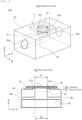
Fig. 3] Fig. 3 is an exploded perspective view and a sectional view illustrating a structure of a pressure sensor module according to Example 1. - [
Fig. 4] Fig. 4 is an exploded perspective view and a sectional view illustrating a structure of a pressure sensor module according to a modification of Example 1. - [
Fig. 5] Fig. 5 is a sectional view illustrating an effect of the pressure sensor module ofFig. 4 . - [
Fig. 6] Fig. 6 is a sectional view illustrating a protrusion according to another modification of Example 1. - [
Fig. 7] Fig. 7 is a sectional view illustrating a protrusion according to still another modification of Example 1. - [
Fig. 8] Fig. 8 is a sectional view illustrating a structure of a pressure sensor module according to Example 2. - [
Fig. 9] Fig. 9 is a sectional view illustrating a structure of a pressure sensor with a cap according to Example 3. - [
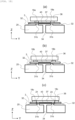
Fig. 10] Fig. 10 is a sectional view illustrating a positional relationship of a cap and a protrusion according to Example 3. - [
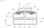
Fig. 11] Fig. 11 is a diagram illustrating a structure of a pressure sensor module according to Example 4. - [
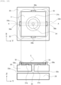
Fig. 12] Fig. 12 is a diagram illustrating a positioning protrusion structure according to Example 5. - [
Fig. 13] Fig. 13 is a plan view illustrating another positioning structure according to Example 5. - [
Fig. 14] Fig. 14 is an exploded perspective view illustrating a structure of a pressure sensor module according to Example 5. - Hereinafter, examples of the present invention will be described with reference to the appended drawings.
- Example 1 of the present invention will be described with reference from
Figs. 1 to 3 . -
Fig. 1 shows a diagram illustrating a basic configuration of a dispensingapparatus 1 according to Example 1. The dispensingapparatus 1 includes apressure sensor module 15. A flow channel system of the dispensingapparatus 1 includes anozzle 2, asyringe pump 4, anelectronic valve 5, agear pump 6, and asystem water tank 7. Each component is connected in relation to apipe 8. - The
syringe pump 4 is composed of a container 9, aplunger 10, aball screw 11, and adrive motor 12. Thedrive motor 12 is controlled by acontrol substrate 14 like a motor that drives asample dispensing mechanism 13 or the like. Thepressure sensor module 15 is included inside anarm 16. Thearm 16 can operate rotatably and vertically to carry a liquid to suction and discharge positions. -
Fig. 2 is a diagram illustrating an inside state of thepipe 8 after suction. The inside of thepipe 8 is filled withsystem water 21 which is transmitted pressure by syringe. By transmitting a pressure from thesyringe pump 4, it is possible to suck and discharge a liquid 22 from thenozzle 2. - When the liquid 22 is sucked from the
nozzle 2, theplunger 10 inside thesyringe pump 4 is pulled in a closed state of theelectronic value 5. Conversely, when the liquid is discharged from thenozzle 2, theplunger 10 inside thesyringe pump 4 is pushed into the container 9 in a state in which theelectronic valve 5 is closed. When the liquid 22 such as a sample is sucked,air segment 23 for segmentation by thenozzle 2 is sucked so that the liquid 22 is not mixed with thesystem water 21 inside thepipe 8, and then the liquid 22 is sucked. - After discharge, cleaning of the
nozzle 2 is performed. In cleaning of thenozzle 2, a cleaning water is brought to the external wall of thenozzle 2 and thesystem water 21 inside the flow channel is pushed out. In the pushing of thesystem water 21 inside thenozzle 2 in cleaning, by opening theelectronic valve 5 and using a pressure of thegear pump 6, thesystem water 21 is driven out at a higher pressure than when the water is pushed out by thesyringe pump 4. - To detect an abnormality such as clogging or idle suction which is likely to occur during a dispensing operation, the
pressure sensor module 15 is included in thepipe 8. Thepressure sensor module 15 monitors a pressure of thesystem water 21 and can detect a change in a pressure occurring when an abnormality such as clogging or idle suction of thenozzle 2 occurs. - In the present example, to detect a change in a pressure of the
nozzle 2 sensitively, thepressure sensor module 15 is installed inside thearm 16 which is at a position as close as possible to thenozzle 2, but a position at which thepressure sensor module 15 is installed is not limited to the inside of thearm 16. For example, thepressure sensor module 15 may be installed along thepipe 8 inside thesample dispensing mechanism 13. - A structure of a
pressure sensor module 15a according to the present example will be described with reference toFig. 3. Fig. 3 is a diagram illustrating a structure of thepressure sensor module 15a according to the present invention. In the present specification and the appended drawings, to facilitate a description, it is assumed that a long-side direction, a short-side direction, and a height direction of thepressure sensor module 15a is the Y direction, the X direction and the Z direction, respectively, but the definition of the directions is not essential in implementation of the present invention. -
Fig. 3(a) is an exploded perspective view of thepressure sensor module 15a andFig. 3(b) is a sectional view of thepressure sensor module 15a. Thepressure sensor module 15a includes aflow channel substrate 25. In theflow channel substrate 25, aflow channel 33 is formed inside, screws (not illustrated) are provided in aflow channel entrance 33a and aflow channel exit 33b, and theflow channel 33 can be connected to thepipe 8 of thedispensing apparatus 1 illustrated inFig. 2 via a joint. - Inside the
flow channel substrate 25, abranch channel 34 branched from theflow channel 33 to the outer surface (in the Z direction) of theflow channel substrate 25 is formed. Thepressure sensor module 15a includes apiezoresistive semiconductor element 3. Thepiezoresistive semiconductor element 3 is disposed to occupy a termination of thebranch channel 34. Thepiezoresistive semiconductor element 3 is an example of a distortion detection unit that detects a pressure. - In this way, the
branch channel 34 is branched from theflow channel 33 and is connected to thepiezoresistive semiconductor element 3 at the termination (one end). - The
piezoresistive semiconductor element 3 is disposed at least partially via thebond layer 32 so that the termination of thebranch channel 34 is occupied. Thepiezoresistive semiconductor element 3 is joined to theflow channel substrate 25 via thebond layer 32. - Near the termination of the
branch channel 34 of theflow channel substrate 25, aprotrusion 31a is provided to surround the termination. In this present example, theprotrusion 31a has an annular structure that surrounds an outer circumference of thebranch channel 34 at the termination. In the present example, theprotrusion 31a is formed as a part of theflow channel substrate 25. Thebond layer 32 is provided to surround the circumference of theprotrusion 31a. - A thickness of the
bond layer 32 can be determined by a height of theprotrusion 31a. In the present example, when it is assumed that the shape of the inner circumference of theprotrusion 31a is circular, a dimension (inner diameter) X1 inside theprotrusion 31a and a dimension (inner diameter) X2 inside thebranch channel 34 have a relationship of X1 = X2. - The
piezoresistive semiconductor element 3 is flexurally deformed with a change in pressure of thesystem water 21 flowing in the flow channel and a change in a resistance value due to the deflection is measured to measure a pressure of thesystem water 21 flowing in a cylinder. - A structure of a
pressure sensor module 15b according to a modification of Example 1 will be described with reference toFig. 4. Fig. 4 is a diagram illustrating the structure of thepressure sensor module 15b according to the present invention.Fig. 4(a) is an exploded perspective view of thepressure sensor module 15b andFig. 4(b) is a sectional view of thepressure sensor module 15b. Hereinafter, a description of common portions to those of Example 1 will be omitted in some cases. - A
protrusion 31b is provided near the termination of thebranch channel 34 of theflow channel substrate 25, and thebond layer 32 is provided to surround the circumference of theprotrusion 31b. Theprotrusion 31b is formed outside of thebranch channel 34. As compared with a dimension (inner diameter) X3 inside thebranch channel 34, a dimension (inner diameter) X1 inside theprotrusion 31b has a relationship of X3 < X1. That is, an inside dimension of theprotrusion 31b is greater than an inside dimension of thebranch channel 34. - The
piezoresistive semiconductor element 3 is deformed with a change in pressure of thesystem water 21 flowing in the flow channel and a change in a resistance value due to the distortion is measured to measure a pressure of thesystem water 21 flowing in a cylinder. - When a pressure is applied to the
branch channel 34 by the system water, a volume of the branch channel in the structure ofFig. 4 is less than a volume of the branch channel illustrated inFig. 3 . Therefore, a structure in which pipe resistance decreases and a response speed of a pressure measurement can be made fast is realized. - On the other hand, a pressure of the system water is also applied to the inner diameter of the
protrusion 31b, thepiezoresistive semiconductor element 3 is flexurally deformed, and the deflection is measured. However, an area contributing to the flexural deformation is determined by the inner diameter of theprotrusion 31b. Therefore, in this structure, an inner diameter dimension of theprotrusion 31b may be greater than an inner diameter dimension of thebranch channel 34. - A material of the
piezoresistive semiconductor element 3 applied toFigs. 3 and4 is preferably silicon. For example, a thickness is preferably 100 µm or less and is more preferably 50 µm or less. When the thickness of the silicon is thin, a deformation region can be expanded with respect to a minute pressure variation, and thus it is possible to improve detection accuracy. - In a thin film processing method for the
piezoresistive semiconductor element 3, grinding and chemical mechanical polishing (CMP) can be applied to form a thin film. In this method, a variation in thickness rarely occurs and the piezoresistive semiconductor element with a uniform thickness can be formed, and thus productivity is excellent. - When the
piezoresistive semiconductor element 3 is formed thinly by thin film processing, an electric leakage possibility is assumed due to the structure of thepiezoresistive semiconductor element 3 or electric conductivity of a silicon material. However, measures can be taken against this, for example, by forming an insulating material of a thin film on the surface of thepiezoresistive semiconductor element 3. To improve adhesion with an adhesive material used in thebond layer 32, a thin metal film or the like may be formed on the surface of thepiezoresistive semiconductor element 3 or the surface of theflow channel substrate 25. - An epoxy-based adhesive, a silver paste, a thermal diffusion bond, a thermosetting adhesive, a UV addition type adhesive, a low-melting point glass, or the like can be applied to the
bond layer 32. As a material of theflow channel substrate 25, stainless steel is preferable and a metal with high corrosion resistance (for example, aluminum or titanium) may be applied. Further, a resin material such as acrylic may be applied. - As an example of a processing method for the
protrusions protrusions piezoresistive semiconductor element 3 and can be freely selected, for example, in the range from tens of microns to a few millimeters. Shapes of theprotrusions - Any heights of the
protrusions piezoresistive semiconductor element 3 is provided directly at the termination of the branch channel is adopted, a change in pressure of the system water flowing in the flow channel can be detected with high accuracy because a distance to the termination of the branch channel is short, and thus there is the advantage that a pressure detection speed is fast. Therefore, as the heights of theprotrusions - As illustrated in
Fig. 3(b) , when protrusion heights of theprotrusions bond layer 32 also accordingly becomes thin. Therefore, it is possible to inhibit expansion of thebond layer 32 in association with a change in condition (an increase in temperature), and thus it is possible to present deformation of thepiezoresistive semiconductor element 3. - In the present example, the
piezoresistive semiconductor element 3 which is the distortion detection unit includes a thin semiconductor element, and thus can measure a pressure with high accuracy. As a modification, a distortion gage, a piezoelectric element, or the like may be applied as the distortion detection unit without being limited to the piezoresistive semiconductor element. - Next, effects of the
protrusion 31b formed in thepiezoresistive semiconductor element 3 will be described with reference toFig. 5. Fig. 5(a) illustrates a reference example for comparison and corresponds to a case where thepiezoresistive semiconductor element 3 is mounted via the bond layer 32 (32a and 32b) in a structure in which no protrusion is formed near the termination of thebranch channel 34 formed inside theflow channel substrate 25. -
Fig. 5(b) corresponds to the configuration ofFig. 4 and illustrates a case where thepiezoresistive semiconductor element 3 is mounted via thebond layer 32 in a structure in which theprotrusion 31b is formed near the termination of thebranch channel 34 formed inside theflow channel substrate 25. - A range in which the
piezoresistive semiconductor element 3 is deformed by a hydraulic pressure is assumed to be adeformation unit 17. InFig. 5 , thedeformation unit 17 is a region of a one-side surface of thepiezoresistive semiconductor element 3, but may be a region penetrating from one surface to the other-side surface of thepiezoresistive semiconductor element 3. - From
Fig. 5(a) , in a structure in which no protrusion is formed on the surface of theflow channel substrate 25, thepiezoresistive semiconductor element 3a is a thin film, and thus handling is difficult, during mounting. Even when a dedicated jig is applied, it can be predicted that mounting in parallel to the surface of theflow channel substrate 25 is difficult. Therefore, an influence of viscosity of thebond layers - As a result, even when a load is applied in parallel, there is a possibility of the
piezoresistive semiconductor element 3 being mounted at an angle which is not 0 and corresponds to adifference 8 in height because of a difference in internal stress of the bond layer (a difference in thickness between thebond layers - When the
piezoresistive semiconductor element 3a is pressed tightly against the bond layer, the bond layer floats in the Y direction. Therefore, even when a necessary deformation region of thepiezoresistive semiconductor element 3 which should be deformed by a hydraulic pressure is a range of X4, an actual deformation region is restricted to a range of X5, and thus there is concern of performance deteriorating. That is, thedeformation unit 17 cannot be deformed outside of the range of X5. - On the other hand, when a bond layer with high viscosity is applied, the bond layer floats in the Y direction at the time of tight pressing of the
piezoresistive semiconductor element 3a against the bond layer. Therefore, the deformation region is restricted similarly, and thus performance deteriorates. - In the configuration of
Fig. 4 , as illustrated inFig. 5(b) , aprotrusion 31b is formed on the surface of theflow channel substrate 25. Therefore, thebond layer 32 does not intrude inside and an extra adhesive projects out to the outer circumference of thepiezoresistive semiconductor element 3b so that the film thickness of the bond layer can be constant. In this example, the height of theprotrusion 31b is equal to the thickness of thebond layer 32, and thus thepiezoresistive semiconductor element 3b can be mounted in parallel to the surface of theflow channel substrate 25. - In this example, an inside area of the
protrusion 31b matches a pressure measurement area (that is, the area of the deformation unit 17) of thepiezoresistive semiconductor element 3b. In such a configuration, thedeformation unit 17 can be deformed in all the appropriate range X4. - As described above, accuracy of pressure measurement is improved in the
pressure sensor modules dispensing apparatus 1 according to Example 1. - There is a possibility of a part (a component that has low viscosity and is easily moved by capillarity) of the
bond layer 32 intruding into a contact portion between theprotrusion 31b and thepiezoresistive semiconductor element 3b. When theprotrusion 31b is provided outside of the deformation region of thepiezoresistive semiconductor element 3b, the deformation region can be appropriately guaranteed even if thebond layer 32 intrudes into the contact portion. - As a modification, another structure can be applied other than the structure in which the protrusion is formed in the
flow channel substrate 25.Fig. 6 is a sectional view illustrating another protrusion structure according to a modification of Example 1. In this example, aprotrusion 31d is formed in thepiezoresistive semiconductor element 3. - The
protrusion 31d is configured to be integrated on the surface of thepiezoresistive semiconductor element 3. As a forming method, for example, a thick-film resist or polydimethylsiloxane (PDMS) is coated on a surface on which a piezoresistor of thepiezoresistive semiconductor element 3 is not formed, and the protrusion can be formed with a thickness of tens of µm by patterning in accordance with a photolithographic technique. In this configuration, it is not necessary to form a protrusion on the surface of theflow channel substrate 25 and a thickness of the bond layer can be determined by a thickness of theprotrusion 31d. -
Fig. 7 is a sectional view illustrating a protrusion structure according to still another modification of Example 1. An object of this example is to cause the thickness of the bond layer and a deformation range by a pressure of thepiezoresistive semiconductor element 3 to be constant. Therefore, as illustrated inFig. 7 , aspacer 31c is pinched and thebond layer 32 is provided around thespacer 31c to fix thepiezoresistive semiconductor element 3. - As material of the
spacer 31c, any of various materials such as stainless steel, resin, a rubber material, and Teflon (registered trademark) can be applied. A cross-sectional shape of thespacer 31c is preferably a rectangle as illustrated in the drawing, but a trapezoid, another rectangle, an ellipse, a circle, or the like can be applied. When a spacer with a circular cross-sectional surface such as an O ring is applied, the deformation may be realized with a pressure applied to thepiezoresistive semiconductor element 3. A 3-dimensional shaping technique may be applied to thespacer 31c other than a forming method by machining. - Example 2 of the present invention will be described with reference to the sectional view of
Fig. 8 . Hereinafter, a description of common portions to those of Example 1 will be omitted in some cases. -
Fig. 8(a) illustrates a structure in which aslope surface 35 is formed in a circumferential shape near the exit of thebranch channel 34 of theflow channel substrate 25.Fig. 8(b) illustrates a structure in which acurved surface 39 is formed in a circumferential shape near the exit of thebranch channel 34 of theflow channel substrate 25. In both the structures, theprotrusion 31b formed in theflow channel substrate 25 is formed outside of the exit of thebranch channel 34. Thebond layer 32 is formed in the outer circumference of theprotrusion 31b. - In the structures of
Fig. 8(a) and 8(b) , chamfered portions are formed on the termination side of thebranch channel 34. The chamfered portion is formed with a tapered surface of which a cross-section has a straight shape in the example ofFig. 8(a) and is formed with a curved surface of which a cross-section has a curved shape in the example ofFig. 8(b) . Since an open structure is realized near the exit of the branch channel of theflow channel substrate 25, a hydraulic pressure is smoothly applied to thepiezoresistive semiconductor element 3 when a pressure of the system water is measured. Therefore, a pressure resistance of the system water decreases and a measurement speed is improved. In this way, another shape may be applied as long as a chamfered structure is realized near the exit of thebranch channel 34 of theflow channel substrate 25. - Example 3 of the present invention will be described. Hereinafter, a description of common portions to those of Example 1 or 2 will be omitted in some cases.
- The piezoresistive semiconductor element is formed finally as a thin film by grinding and chemical mechanical polishing. Therefore, there is a possibility of the simplex piezoresistive semiconductor element formed as the thin film being damaged when the piezoresistive semiconductor element is joined to the
flow channel substrate 25. - A configuration according to Example 3 will be described with reference to the sectional view of
Fig. 9 as a structure for preventing damage and improving handling at the time of joining in the simplex piezoresistive semiconductor element. - As illustrated in
Fig. 9 , the pressure sensor module includes acap 36 that covers thepiezoresistive semiconductor element 3 from the upper side (opposite side of the branch channel 34). Thecap 36 is joined with thepiezoresistive semiconductor element 3 by aresin bond layer 18. Aspace 37 is formed between thepiezoresistive semiconductor element 3 and thecap 36. A structure in which a deformed portion does not come into contact with thecap 36 is realized even when thepiezoresistive semiconductor element 3 is deformed because of application of a pressure. - Since an electrode pad for exchanging an electrical signal with the outside is formed in the periphery of the end of the
piezoresistive semiconductor element 3 in some cases, a dimension of thecap 36 may be formed to be smaller than the outer diameter dimension of thepiezoresistive semiconductor element 3. - As a material of the
cap 36, silicon or glass can be applied. As a material of theresin bond layer 18, a polymer material such as benzocyclobutene can be applied. The material is a material that enables a thick film to be formed and can be patterned and a bonding strength can be obtained by adding a temperature. - Next, a positional relationship between the
resin bond layer 18 and theprotrusion 31b formed on the surface of theflow channel substrate 25 will be described with reference to the sectional view ofFig. 10 . In thepiezoresistive semiconductor element 3, a region deformed with application of a pressure is referred to as adeformation unit 40. InFig. 10 , thedeformation unit 40 is a region of a one-side surface of thepiezoresistive semiconductor element 3, but may be a region penetrating from a one-side surface to the other-side surface of thepiezoresistive semiconductor element 3. -
Fig. 10(a) illustrates a case where an inside dimension (inner diameter) of aresin bond layer 18a formed in thecap 36 is the same as an inside dimension (inner diameter) of theprotrusion 31b formed in theflow channel substrate 25. In this example, in deformation of thepiezoresistive semiconductor element 3 by a hydraulic pressure, thedeformation unit 40 is displaced in the Z direction within a range of the dimension (the inner diameter) of theresin bond layer 18a formed below thecap 36. -
Fig. 10(b) illustrates a state where aresin bond layer 18b formed in thecap 36 and theprotrusion 31b formed in theflow channel substrate 25 overlap each other partially. In this example, in deformation of thepiezoresistive semiconductor element 3 by a hydraulic pressure, thedeformation unit 40 is displaced in the Z direction within a range of the inner diameter of theresin bond layer 18b formed below thecap 36. - On the other hand,
Fig. 10(c) illustrates a case where the inside dimension (inner diameter) of aresin bond layer 18c formed in thecap 36 is greater than an outside dimension (outer diameter) of theprotrusion 31b formed in theflow channel substrate 25. In this structure, when thepiezoresistive semiconductor element 3 is joined with thebond layer 32 interposed therebetween, positions of theresin bond layer 18c formed in thecap 36 and theprotrusion 31b do not match when viewed in the Z direction. Therefore, acrack 24 occurs inside thepiezoresistive semiconductor element 3 due to shearing stress at the time of bond, and there is a possibility of breaking. Therefore, a reinforcement structure or the like for preventing the crack is necessary. - To avoid such a reinforcement structure, as illustrated in
Figs. 10(a) and 10(b) , a region where thecap 36 comes into contact with thepiezoresistive semiconductor element 3 and a region where theprotrusion 31b comes into contact with thepiezoresistive semiconductor element 3 may overlap each other at least partially when viewed in an axial direction of thebranch channel 34. - Example 4 of the present invention will be described with reference to
Fig. 11 . Hereinafter, a description of common portions to those of any of Example 1 to 3 will be omitted in some cases. -
Fig. 11 is a sectional view illustrating another structure of theflow channel substrate 25 according to the present example. Example 4 differs from Examples 1 to 3 in that theflow channel substrate 25 includes agroove 19 outside of an outer edge of theprotrusion 31b and a part of thebond layer 32 can be disposed in thegroove 19. Since the other configurations are similar to those of the other examples (for example,Fig. 9 ), description thereof will be omitted. - By applying such a structure, a surface area of a contact portion between the
bond layer 32 and theflow channel substrate 25 can increase and the thickness of thebond layer 32 can be sufficiently guaranteed. Therefore, it is possible to improve an adhesive strength of thebond layer 32. It is possible to decrease a projection amount to the outer circumference of thebond layer 32. - Example 5 of the present invention will be described with reference to
Fig. 12 . Hereinafter, description of common portions to those of any of Example 1 to 4 will be omitted in some cases. -
Fig. 12 is a plan view and a sectional view illustrating a structure of theflow channel substrate 25 according to the present example. Positioningprotrusions 38a for positioning a position of thepiezoresistive semiconductor element 3 are formed in theflow channel substrate 25. Thepositioning protrusions 38a project in the Z direction from theflow channel substrate 25. In the present example, thepositioning protrusions 38a are installed at four locations and thepiezoresistive semiconductor element 3 is installed inside thepositioning protrusions 38a. Thepositioning protrusion 38a regulates movement of thepiezoresistive semiconductor element 3 on an XY plane, which facilitates positioning. - In such a configuration, a relative position to the
branch channel 34 and theprotrusion 31b formed in theflow channel substrate 25 can be determined with high precision when thepiezoresistive semiconductor element 3 which is a thin film is disposed. In such a structure, the position of thebranch channel 34 formed in theflow channel substrate 25 can match the positions of theprotrusion 31b and thepiezoresistive semiconductor element 3 with accuracy of tens of microns, and thus measurement accuracy becomes good even in deformation by a hydraulic pressure and a variation among products can be reduced. - The
positioning protrusions 38a may be formed in the entire circumference of thepiezoresistive semiconductor element 3. In the present example, however, thepositioning protrusions 38a are partially disposed so that thebond layer 32 does not obstruct a projection amount to the outer circumference. - The
positioning protrusions 38a can be applied to the structure illustrated inFig. 12 , but other positioning protrusions can be applied as a modification of Example 4. -
Fig. 13 are plan views of various modifications.Fig. 13(a) illustrates an example in which positioningprotrusions 38b disposed in corners of thepiezoresistive semiconductor element 3 are disposed at two locations. When the positioningprotrusions 38b are disposed in the corners, planar portions are preferably present in the X and Y directions. The corners of the positioningprotrusions 38b intersecting in the X and Y directions may be chamfered as illustrated. In this configuration, positioning can be achieved with a small number ofpositioning protrusions 38b. -
Fig. 13(b) illustrates an example in whichcircular positioning protrusions 38c are disposed in middle portions of thepiezoresistive semiconductor element 3 in the X and Y directions. For thepositioning protrusions 38c, a structure in which pin holes or screw holes are formed in theflow channel substrate 25 and pins are installed or a structure in which screws are inserted can be applied. In this structure, the positioning protrusions can be formed at low cost. In this configuration, the positioningprotrusions 38c can also have a pin or screw function. -
Fig. 13(c) illustrates an example in which some ofpositioning protrusions 38d are disposed at positions corresponding to the center of thepiezoresistive semiconductor element 3 in the X direction and thepositioning protrusions 38d are disposed at positions deviating from the center of thepiezoresistive semiconductor element 3 in the Y direction. In the present example, in a positioning method for thepiezoresistive semiconductor element 3, another structure may be used as long as the positioning protrusions are put in the outer circumference. - Next, an electric wiring example in the
piezoresistive semiconductor element 3 mounted on apressure sensor module 15c is illustrated in an exploded perspective view ofFig. 14 . Thepiezoresistive semiconductor element 3 is mounted inside a region demarcated by thepositioning protrusions 38a. - A plurality of
electrode pads 42b are located in thepiezoresistive semiconductor element 3 and are connected betweenwires 43 andelectrodes pads 42a formed in an electric wiringflexible substrate 41. Gold wires and aluminum wires can be applied as thewires 43. Besides, an anisotropic conductive film (ACF) or the like may be applied for the connection. - When the system water flows in the
flow channel 33, the system water flows in thebranch channel 34 and a pressure is applied to thepiezoresistive semiconductor element 3. When the pressure is applied, thepiezoresistive semiconductor element 3 is deformed. The deformation is transmitted as an electric signal to theflexible substrate 41 to measure the pressure. - The present invention is not limited to the above-described examples, but various modifications and equivalent configurations are included within the gist of the scope of the appended claims. For example, the above-described examples have been described in detail to facilitate the description of the present invention and the present invention is not necessarily limited to all the described configurations. A part of a configuration according to a certain embodiment or modification can be replaced with a configuration according to another embodiment or modification, or a configuration according to another embodiment or modification can also be added to a configuration according to a certain embodiment or modification. Another configuration can be added to, deleted from or replaced with a part of a configuration according to each example or modification.
-
- 1:
- dispensing apparatus
- 2:
- nozzle
- 3, 3a, 3b:
- piezoresistive semiconductor element (distortion detection unit)
- 4:
- syringe pump
- 5:
- electronic valve
- 6:
- gear pump
- 7:
- system water tank
- 8:
- pipe
- 9:
- container
- 10:
- plunger
- 11:
- ball screw
- 12:
- drive motor
- 13:
- sample dispensing mechanism
- 14:
- control substrate
- 15, 15a, 15b, 15c:
- pressure sensor module
- 16:
- arm
- 17:
- deformation unit
- 18, 18a, 18b, 18c:
- resin bond layer
- 19:
- groove
- 21:
- system water
- 22:
- liquid
- 23:
- air segment
- 24:
- crack
- 25:
- flow channel substrate
- 31, 31a, 31b, 31d:
- protrusions
- 31c:
- spacer
- 32, 32a, 32b:
- bond layer
- 33:
- flow channel
- 33a:
- flow channel entrance
- 33b:
- flow channel exit
- 34:
- branch channel
- 35:
- slope surface
- 36:
- cap
- 37:
- space
- 38a, 38b, 38c, 38d:
- protrusions
- 39:
- curved surface
- 40:
- deformation unit
- 41:
- flexible substrate
- 42a, 42b:
- electrode pad
- 43:
- wire
- All publications, patents, and patent applications cited in the present specification are claimed to be incorporated in the present specification.
Claims (13)
- A pressure sensor module comprising:a flow channel substrate in which a flow channel and a branch channel are formed; anda distortion detection unit configured to detect a pressure,wherein the branch channel is branched from the flow channel and is connected to the distortion detection unit at one end of the branch channel,wherein the distortion detection unit is disposed at least partially via a bond layer to block the one end of the branch channel, andwherein a protrusion is provided to surround the one end of the branch channel.
- The pressure sensor module according to claim 1, wherein an inside dimension of the protrusion is greater than an inside dimension of the branch channel.
- The pressure sensor module according to claim 2, wherein the protrusion is formed in the distortion detection unit.
- The pressure sensor module according to claim 2, wherein a height of the protrusion is equal to a thickness of the bond layer.
- The pressure sensor module according to claim 1, wherein an inside area of the protrusion matches a pressure measurement area of the distortion detection unit.
- The pressure sensor module according to claim 1, wherein a height of the protrusion is 50 µm or less.
- The pressure sensor module according to claim 1, wherein the flow channel substrate includes a groove outside of an outer edge of the protrusion.
- The pressure sensor module according to claim 2, wherein a chamfered portion is provided at the one end of the branch channel.
- The pressure sensor module according to claim 1, further comprising a cap configured to cover the distortion detection unit on an opposite side of the branch channel.
- The pressure sensor module according to claim 9, wherein, when viewed in an axial direction of the branch channel, a region where the cap comes into contact with the distortion detection unit and a region where the protrusion comes into contact with the distortion detection unit overlap at least partially.
- The pressure sensor module according to claim 1, wherein a positioning protrusion for positioning the distortion detection unit is formed in the flow channel substrate.
- The pressure sensor module according to claim 1, wherein the distortion detection unit includes a thin semiconductor element.
- A dispensing apparatus comprising the pressure sensor module according to claim 1.
Applications Claiming Priority (2)
| Application Number | Priority Date | Filing Date | Title |
|---|---|---|---|
| JP2021081572A JP7577026B2 (en) | 2021-05-13 | 2021-05-13 | Pressure sensor module and dispensing device |
| PCT/JP2022/017532 WO2022239589A1 (en) | 2021-05-13 | 2022-04-11 | Pressure sensor module and dispensing device |
Publications (2)
| Publication Number | Publication Date |
|---|---|
| EP4339574A1 true EP4339574A1 (en) | 2024-03-20 |
| EP4339574A4 EP4339574A4 (en) | 2025-04-09 |
Family
ID=84028229
Family Applications (1)
| Application Number | Title | Priority Date | Filing Date |
|---|---|---|---|
| EP22801005.4A Pending EP4339574A4 (en) | 2021-05-13 | 2022-04-11 | PRESSURE SENSOR MODULE AND DISPENSING DEVICE |
Country Status (5)
| Country | Link |
|---|---|
| US (1) | US12644788B2 (en) |
| EP (1) | EP4339574A4 (en) |
| JP (1) | JP7577026B2 (en) |
| CN (1) | CN116981922A (en) |
| WO (1) | WO2022239589A1 (en) |
Families Citing this family (4)
| Publication number | Priority date | Publication date | Assignee | Title |
|---|---|---|---|---|
| LU101845B1 (en) * | 2020-06-10 | 2021-12-10 | Rotarex S A | Pressure sensor formed by strain gauge on a deformable membrane of a fluid device |
| JP7592191B2 (en) * | 2021-11-05 | 2024-11-29 | 株式会社日立ハイテク | Pressure sensor and dispensing device |
| JP7846028B2 (en) * | 2023-01-17 | 2026-04-14 | 株式会社日立ハイテク | Pressure sensor module, method for manufacturing a pressure sensor module |
| JP2025072747A (en) | 2023-10-25 | 2025-05-12 | 株式会社日立ハイテク | Fluid Sensor Module |
Family Cites Families (11)
| Publication number | Priority date | Publication date | Assignee | Title |
|---|---|---|---|---|
| JPS5828876A (en) * | 1981-08-12 | 1983-02-19 | Mitsubishi Electric Corp | Semiconductor pressure sensor |
| US4825876A (en) * | 1988-02-23 | 1989-05-02 | Abbott Laboratories | Encapsulated blood pressure transducer |
| JPH02291838A (en) * | 1989-05-02 | 1990-12-03 | Nec Corp | Disposable blood pressure transducer |
| JPH07174654A (en) * | 1993-12-20 | 1995-07-14 | Hokuriku Electric Ind Co Ltd | Pressure sensor |
| JP3593397B2 (en) * | 1995-11-02 | 2004-11-24 | 北陸電気工業株式会社 | Semiconductor pressure sensor |
| JP2000111435A (en) | 1998-10-08 | 2000-04-21 | Saginomiya Seisakusho Inc | Combustion pressure sensor |
| JP4444424B2 (en) | 2000-01-21 | 2010-03-31 | 株式会社フジクラ | Semiconductor pressure sensor |
| JP6253825B1 (en) | 2017-03-03 | 2017-12-27 | 三菱電機株式会社 | Semiconductor differential pressure sensor |
| US10655989B2 (en) | 2017-09-12 | 2020-05-19 | Silicon Microstructures, Inc. | Pressure sensor cap having flow path with dimension variation |
| JP2020071191A (en) | 2018-11-02 | 2020-05-07 | 株式会社日立ハイテク | Dispenser |
| JP2021081572A (en) | 2019-11-19 | 2021-05-27 | 京セラドキュメントソリューションズ株式会社 | Display control unit, image processing apparatus, and display control method |
-
2021
- 2021-05-13 JP JP2021081572A patent/JP7577026B2/en active Active
-
2022
- 2022-04-11 CN CN202280019264.4A patent/CN116981922A/en active Pending
- 2022-04-11 WO PCT/JP2022/017532 patent/WO2022239589A1/en not_active Ceased
- 2022-04-11 EP EP22801005.4A patent/EP4339574A4/en active Pending
- 2022-04-11 US US18/279,448 patent/US12644788B2/en active Active
Also Published As
| Publication number | Publication date |
|---|---|
| JP7577026B2 (en) | 2024-11-01 |
| WO2022239589A1 (en) | 2022-11-17 |
| EP4339574A4 (en) | 2025-04-09 |
| JP2022175292A (en) | 2022-11-25 |
| US20240133757A1 (en) | 2024-04-25 |
| US20240230441A9 (en) | 2024-07-11 |
| CN116981922A (en) | 2023-10-31 |
| US12644788B2 (en) | 2026-06-02 |
Similar Documents
| Publication | Publication Date | Title |
|---|---|---|
| US20240230441A9 (en) | Pressure Sensor Module and Dispensing Device | |
| US8230745B2 (en) | Wet/wet differential pressure sensor based on microelectronic packaging process | |
| CN102105769B (en) | Media isolated differential pressure sensor with cap | |
| US6729181B2 (en) | Flow sensor in a housing | |
| US7216547B1 (en) | Pressure sensor with silicon frit bonded cap | |
| US8033180B2 (en) | Flow sensor apparatus and method with media isolated electrical connections | |
| JP7574472B2 (en) | Pressure sensor module and dispensing device having pressure sensor module | |
| CN110174210A (en) | Pressure sensor and its packaging method | |
| JP7817080B2 (en) | Pressure Sensor | |
| US20120211517A1 (en) | Metering device | |
| US11344207B2 (en) | Pressure pulse wave sensor and biological information measurement device | |
| JP2025072747A (en) | Fluid Sensor Module | |
| JP7846028B2 (en) | Pressure sensor module, method for manufacturing a pressure sensor module | |
| JP2020071191A (en) | Dispenser | |
| Hassan et al. | world’s smallest, membrane-based capacitive differential pressure sensor-package structure, material selection, assembly challenges and solutions | |
| JPH04267566A (en) | Semiconductor pressure sensor for high pressure | |
| EP4148406B1 (en) | Sensing components comprising coupling elements | |
| TWI742469B (en) | Biochip package structure | |
| CN121994400A (en) | Pressure sensor and pressure interface thereof |
Legal Events
| Date | Code | Title | Description |
|---|---|---|---|
| STAA | Information on the status of an ep patent application or granted ep patent |
Free format text: STATUS: UNKNOWN |
|
| STAA | Information on the status of an ep patent application or granted ep patent |
Free format text: STATUS: THE INTERNATIONAL PUBLICATION HAS BEEN MADE |
|
| PUAI | Public reference made under article 153(3) epc to a published international application that has entered the european phase |
Free format text: ORIGINAL CODE: 0009012 |
|
| STAA | Information on the status of an ep patent application or granted ep patent |
Free format text: STATUS: REQUEST FOR EXAMINATION WAS MADE |
|
| 17P | Request for examination filed |
Effective date: 20230830 |
|
| AK | Designated contracting states |
Kind code of ref document: A1 Designated state(s): AL AT BE BG CH CY CZ DE DK EE ES FI FR GB GR HR HU IE IS IT LI LT LU LV MC MK MT NL NO PL PT RO RS SE SI SK SM TR |
|
| DAV | Request for validation of the european patent (deleted) | ||
| DAX | Request for extension of the european patent (deleted) | ||
| A4 | Supplementary search report drawn up and despatched |
Effective date: 20250311 |
|
| RIC1 | Information provided on ipc code assigned before grant |
Ipc: G01L 19/00 20060101ALI20250306BHEP Ipc: G01L 9/00 20060101AFI20250306BHEP |