EP4333042A2 - High-electron-mobility transistor - Google Patents
High-electron-mobility transistor Download PDFInfo
- Publication number
- EP4333042A2 EP4333042A2 EP23186269.9A EP23186269A EP4333042A2 EP 4333042 A2 EP4333042 A2 EP 4333042A2 EP 23186269 A EP23186269 A EP 23186269A EP 4333042 A2 EP4333042 A2 EP 4333042A2
- Authority
- EP
- European Patent Office
- Prior art keywords
- mode gate
- gate
- semiconductor material
- depletion mode
- island
- Prior art date
- Legal status (The legal status is an assumption and is not a legal conclusion. Google has not performed a legal analysis and makes no representation as to the accuracy of the status listed.)
- Pending
Links
Images



Classifications
-
- H—ELECTRICITY
- H10—SEMICONDUCTOR DEVICES; ELECTRIC SOLID-STATE DEVICES NOT OTHERWISE PROVIDED FOR
- H10D—INORGANIC ELECTRIC SEMICONDUCTOR DEVICES
- H10D84/00—Integrated devices formed in or on semiconductor substrates that comprise only semiconducting layers, e.g. on Si wafers or on GaAs-on-Si wafers
- H10D84/80—Integrated devices formed in or on semiconductor substrates that comprise only semiconducting layers, e.g. on Si wafers or on GaAs-on-Si wafers characterised by the integration of at least one component covered by groups H10D12/00 or H10D30/00, e.g. integration of IGFETs
- H10D84/82—Integrated devices formed in or on semiconductor substrates that comprise only semiconducting layers, e.g. on Si wafers or on GaAs-on-Si wafers characterised by the integration of at least one component covered by groups H10D12/00 or H10D30/00, e.g. integration of IGFETs of only field-effect components
-
- H—ELECTRICITY
- H10—SEMICONDUCTOR DEVICES; ELECTRIC SOLID-STATE DEVICES NOT OTHERWISE PROVIDED FOR
- H10D—INORGANIC ELECTRIC SEMICONDUCTOR DEVICES
- H10D30/00—Field-effect transistors [FET]
- H10D30/40—FETs having zero-dimensional [0D], one-dimensional [1D] or two-dimensional [2D] charge carrier gas channels
- H10D30/47—FETs having zero-dimensional [0D], one-dimensional [1D] or two-dimensional [2D] charge carrier gas channels having two-dimensional [2D] charge carrier gas channels, e.g. nanoribbon FETs or high electron mobility transistors [HEMT]
- H10D30/471—High electron mobility transistors [HEMT] or high hole mobility transistors [HHMT]
- H10D30/475—High electron mobility transistors [HEMT] or high hole mobility transistors [HHMT] having wider bandgap layer formed on top of lower bandgap active layer, e.g. undoped barrier HEMTs such as i-AlGaN/GaN HEMTs
- H10D30/4755—High electron mobility transistors [HEMT] or high hole mobility transistors [HHMT] having wider bandgap layer formed on top of lower bandgap active layer, e.g. undoped barrier HEMTs such as i-AlGaN/GaN HEMTs having wide bandgap charge-carrier supplying layers, e.g. modulation doped HEMTs such as n-AlGaAs/GaAs HEMTs
-
- H—ELECTRICITY
- H10—SEMICONDUCTOR DEVICES; ELECTRIC SOLID-STATE DEVICES NOT OTHERWISE PROVIDED FOR
- H10D—INORGANIC ELECTRIC SEMICONDUCTOR DEVICES
- H10D1/00—Resistors, capacitors or inductors
- H10D1/01—Manufacture or treatment
- H10D1/045—Manufacture or treatment of capacitors having potential barriers, e.g. varactors
- H10D1/047—Manufacture or treatment of capacitors having potential barriers, e.g. varactors of conductor-insulator-semiconductor capacitors, e.g. trench capacitors
-
- H—ELECTRICITY
- H10—SEMICONDUCTOR DEVICES; ELECTRIC SOLID-STATE DEVICES NOT OTHERWISE PROVIDED FOR
- H10D—INORGANIC ELECTRIC SEMICONDUCTOR DEVICES
- H10D1/00—Resistors, capacitors or inductors
- H10D1/60—Capacitors
- H10D1/62—Capacitors having potential barriers
- H10D1/66—Conductor-insulator-semiconductor capacitors, e.g. MOS capacitors
-
- H—ELECTRICITY
- H10—SEMICONDUCTOR DEVICES; ELECTRIC SOLID-STATE DEVICES NOT OTHERWISE PROVIDED FOR
- H10D—INORGANIC ELECTRIC SEMICONDUCTOR DEVICES
- H10D30/00—Field-effect transistors [FET]
- H10D30/01—Manufacture or treatment
- H10D30/015—Manufacture or treatment of FETs having heterojunction interface channels or heterojunction gate electrodes, e.g. HEMT
-
- H—ELECTRICITY
- H10—SEMICONDUCTOR DEVICES; ELECTRIC SOLID-STATE DEVICES NOT OTHERWISE PROVIDED FOR
- H10D—INORGANIC ELECTRIC SEMICONDUCTOR DEVICES
- H10D30/00—Field-effect transistors [FET]
- H10D30/40—FETs having zero-dimensional [0D], one-dimensional [1D] or two-dimensional [2D] charge carrier gas channels
- H10D30/47—FETs having zero-dimensional [0D], one-dimensional [1D] or two-dimensional [2D] charge carrier gas channels having two-dimensional [2D] charge carrier gas channels, e.g. nanoribbon FETs or high electron mobility transistors [HEMT]
- H10D30/471—High electron mobility transistors [HEMT] or high hole mobility transistors [HHMT]
- H10D30/475—High electron mobility transistors [HEMT] or high hole mobility transistors [HHMT] having wider bandgap layer formed on top of lower bandgap active layer, e.g. undoped barrier HEMTs such as i-AlGaN/GaN HEMTs
-
- H—ELECTRICITY
- H10—SEMICONDUCTOR DEVICES; ELECTRIC SOLID-STATE DEVICES NOT OTHERWISE PROVIDED FOR
- H10D—INORGANIC ELECTRIC SEMICONDUCTOR DEVICES
- H10D62/00—Semiconductor bodies, or regions thereof, of devices having potential barriers
- H10D62/10—Shapes, relative sizes or dispositions of the regions of the semiconductor bodies; Shapes of the semiconductor bodies
- H10D62/17—Semiconductor regions connected to electrodes not carrying current to be rectified, amplified or switched, e.g. channel regions
- H10D62/343—Gate regions of field-effect devices having PN junction gates
-
- H—ELECTRICITY
- H10—SEMICONDUCTOR DEVICES; ELECTRIC SOLID-STATE DEVICES NOT OTHERWISE PROVIDED FOR
- H10D—INORGANIC ELECTRIC SEMICONDUCTOR DEVICES
- H10D62/00—Semiconductor bodies, or regions thereof, of devices having potential barriers
- H10D62/80—Semiconductor bodies, or regions thereof, of devices having potential barriers characterised by the materials
- H10D62/85—Semiconductor bodies, or regions thereof, of devices having potential barriers characterised by the materials being Group III-V materials, e.g. GaAs
- H10D62/8503—Nitride Group III-V materials, e.g. AlN or GaN
-
- H—ELECTRICITY
- H10—SEMICONDUCTOR DEVICES; ELECTRIC SOLID-STATE DEVICES NOT OTHERWISE PROVIDED FOR
- H10D—INORGANIC ELECTRIC SEMICONDUCTOR DEVICES
- H10D64/00—Electrodes of devices having potential barriers
- H10D64/111—Field plates
-
- H—ELECTRICITY
- H10—SEMICONDUCTOR DEVICES; ELECTRIC SOLID-STATE DEVICES NOT OTHERWISE PROVIDED FOR
- H10D—INORGANIC ELECTRIC SEMICONDUCTOR DEVICES
- H10D64/00—Electrodes of devices having potential barriers
- H10D64/111—Field plates
- H10D64/112—Field plates comprising multiple field plate segments
-
- H—ELECTRICITY
- H10—SEMICONDUCTOR DEVICES; ELECTRIC SOLID-STATE DEVICES NOT OTHERWISE PROVIDED FOR
- H10D—INORGANIC ELECTRIC SEMICONDUCTOR DEVICES
- H10D64/00—Electrodes of devices having potential barriers
- H10D64/20—Electrodes characterised by their shapes, relative sizes or dispositions
- H10D64/27—Electrodes not carrying the current to be rectified, amplified, oscillated or switched, e.g. gates
- H10D64/311—Gate electrodes for field-effect devices
- H10D64/411—Gate electrodes for field-effect devices for FETs
- H10D64/511—Gate electrodes for field-effect devices for FETs for IGFETs
- H10D64/512—Disposition of the gate electrodes, e.g. buried gates
-
- H—ELECTRICITY
- H10—SEMICONDUCTOR DEVICES; ELECTRIC SOLID-STATE DEVICES NOT OTHERWISE PROVIDED FOR
- H10D—INORGANIC ELECTRIC SEMICONDUCTOR DEVICES
- H10D64/00—Electrodes of devices having potential barriers
- H10D64/20—Electrodes characterised by their shapes, relative sizes or dispositions
- H10D64/27—Electrodes not carrying the current to be rectified, amplified, oscillated or switched, e.g. gates
- H10D64/311—Gate electrodes for field-effect devices
- H10D64/411—Gate electrodes for field-effect devices for FETs
- H10D64/511—Gate electrodes for field-effect devices for FETs for IGFETs
- H10D64/517—Gate electrodes for field-effect devices for FETs for IGFETs characterised by the conducting layers
- H10D64/518—Gate electrodes for field-effect devices for FETs for IGFETs characterised by the conducting layers characterised by their lengths or sectional shapes
-
- H—ELECTRICITY
- H10—SEMICONDUCTOR DEVICES; ELECTRIC SOLID-STATE DEVICES NOT OTHERWISE PROVIDED FOR
- H10D—INORGANIC ELECTRIC SEMICONDUCTOR DEVICES
- H10D84/00—Integrated devices formed in or on semiconductor substrates that comprise only semiconducting layers, e.g. on Si wafers or on GaAs-on-Si wafers
- H10D84/01—Manufacture or treatment
-
- H—ELECTRICITY
- H10—SEMICONDUCTOR DEVICES; ELECTRIC SOLID-STATE DEVICES NOT OTHERWISE PROVIDED FOR
- H10D—INORGANIC ELECTRIC SEMICONDUCTOR DEVICES
- H10D84/00—Integrated devices formed in or on semiconductor substrates that comprise only semiconducting layers, e.g. on Si wafers or on GaAs-on-Si wafers
- H10D84/01—Manufacture or treatment
- H10D84/0123—Integrating together multiple components covered by H10D12/00 or H10D30/00, e.g. integrating multiple IGBTs
- H10D84/0126—Integrating together multiple components covered by H10D12/00 or H10D30/00, e.g. integrating multiple IGBTs the components including insulated gates, e.g. IGFETs
- H10D84/0158—Integrating together multiple components covered by H10D12/00 or H10D30/00, e.g. integrating multiple IGBTs the components including insulated gates, e.g. IGFETs the components including FinFETs
-
- H—ELECTRICITY
- H10—SEMICONDUCTOR DEVICES; ELECTRIC SOLID-STATE DEVICES NOT OTHERWISE PROVIDED FOR
- H10D—INORGANIC ELECTRIC SEMICONDUCTOR DEVICES
- H10D84/00—Integrated devices formed in or on semiconductor substrates that comprise only semiconducting layers, e.g. on Si wafers or on GaAs-on-Si wafers
- H10D84/01—Manufacture or treatment
- H10D84/02—Manufacture or treatment characterised by using material-based technologies
- H10D84/05—Manufacture or treatment characterised by using material-based technologies using Group III-V technology
-
- H—ELECTRICITY
- H10—SEMICONDUCTOR DEVICES; ELECTRIC SOLID-STATE DEVICES NOT OTHERWISE PROVIDED FOR
- H10D—INORGANIC ELECTRIC SEMICONDUCTOR DEVICES
- H10D84/00—Integrated devices formed in or on semiconductor substrates that comprise only semiconducting layers, e.g. on Si wafers or on GaAs-on-Si wafers
- H10D84/80—Integrated devices formed in or on semiconductor substrates that comprise only semiconducting layers, e.g. on Si wafers or on GaAs-on-Si wafers characterised by the integration of at least one component covered by groups H10D12/00 or H10D30/00, e.g. integration of IGFETs
- H10D84/811—Combinations of field-effect devices and one or more diodes, capacitors or resistors
Definitions
- the present disclosure relates to semiconductor structures and, more particularly, to a high-electron-mobility transistor and methods of manufacture.
- a high-electron-mobility transistor is a field-effect transistor incorporating a junction between two materials with different band gaps (i.e. a heterojunction) as the channel, instead of a doped region (as is generally the case for a MOSFET).
- a heterojunction a field-effect transistor incorporating a junction between two materials with different band gaps (i.e. a heterojunction) as the channel, instead of a doped region (as is generally the case for a MOSFET).
- Commonly used material combinations are GaN or GaAs, although other materials can be used dependent on the application of the device.
- HEMT transistors are able to operate at higher frequencies than ordinary transistors, up to millimeter wave frequencies. As the HEMT transistors are able to operate at higher frequencies, they can be used in high-frequency products such as cell phones, satellite television receivers, voltage converters, and radar equipment. For example, a HEMT may be used in satellite receivers and in low power amplifiers.
- Depletion mode pinch off voltages in enhancement mode flows are typically higher than -6V; however, a layout programmable depletion mode pinch off of less than -6V is needed for GaN integrated circuit development, e.g., for building a low voltage reference, etc. Hence control of Vpinch becomes critical.
- a structure comprises: at least one depletion mode gate on a conductive material over a semiconductor material; and at least one enhancement mode gate electrically connected to the at least one depletion mode gate.
- a structure comprises: a metal-insulator-semiconductor (MIS) capacitor, the MIS capacitor comprising a metal plate over a common conducting channel; and an island of semiconductor material over a semiconductor substrate and electrically connected to the MIS capacitor.
- MIS metal-insulator-semiconductor
- a method comprises: forming at least one depletion mode gate comprising a field plate on a conductive material over a semiconductor material; and forming at least one enhancement mode gate electrically connected to the at least one depletion mode gate.
- the present disclosure relates to semiconductor structures and, more particularly, to a high-electron-mobility transistor and methods of manufacture. More specifically, the present disclosure provides structures for depletion mode GaN HEMT Vt control. Advantageously, the present disclosure provides a dedicated depletion mode gate which provides significant improvement in gate control and subthreshold behavior. Also, no additional process complexity is required to generate multiple threshold depletion modes (d-modes).
- d-modes threshold depletion modes
- the high-electron-mobility transistor may be a GaN HEMT with two gates, e.g., depletion mode gate and enhancement mode gate, connected together and, in embodiments, an isolation region (e.g., implant or shallow trench isolation structure)) placed between the two gates.
- the first gate metal may be set for depletion mode operation and the second gate metal (enhancement mode gate) may be set for enhancement mode operation.
- the enhancement mode gate and the depletion mode gate may utilize field plates that are formed in a same deposition and patterning process.
- the depletion mode gate forms part of a metal-insulator-semiconductor (MIS) capacitor and the enhancement mode gate may be composed of an epitaxially grown p-type doped GaN layer.
- MIS metal-insulator-semiconductor
- islands of the pGaN may be connected to MIS regions (depletion mode gate) by a common gate conductor.
- the enhancement mode gate and the MIS region may be separately connected.
- the HEMTs of the present disclosure can be manufactured in a number of ways using a number of different tools.
- the methodologies and tools are used to form structures with dimensions in the micrometer and nanometer scale.
- the methodologies, i.e., technologies, employed to manufacture the HEMTs of the present disclosure have been adopted from integrated circuit (IC) technology.
- the structures are built on wafers and are realized in films of material patterned by photolithographic processes on the top of a wafer.
- the fabrication of the HEMTs uses three basic building blocks: (i) deposition of thin films of material on a substrate, (ii) applying a patterned mask on top of the films by photolithographic imaging, and (iii) etching the films selectively to the mask.
- precleaning processes may be used to clean etched surfaces of any contaminants, as is known in the art.
- rapid thermal anneal processes may be used to drive-in dopants or material layers as is known in the art.
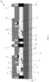
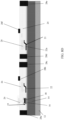
- FIG. 1 shows a HEMT with an enhancement mode gate and a depletion mode gate, and respective fabrication processes in accordance with aspects of the present disclosure.
- the enhancement mode gate and depletion mode gate may be integrated into a single wafer (substrate) with the depletion mode gate using a same field plate (as the gate) as the field plate for the enhancement mode gate.
- the structure of FIG. 1 includes a semiconductor substrate 12 with a semiconductor material 14 on the semiconductor substrate 12.
- the semiconductor material 14 may be AlGaN/GaN, which acts as a conducting channel for the HEMT device, e.g., enhancement mode gate (e-mode gate) and the depletion mode gate (d-mode gate).
- the semiconductor substrate 12 may be composed of any suitable material including, but not limited to, Si, SiGe, SiGeC, SiC, GaAs, InAs, InP, and other III/V or II/VI compound semiconductors.
- the semiconductor substrate 12 comprises p-type Si material with a suitable crystal orientation, e.g., (111).
- a semiconductor material 16 and conductive material 18 may be formed, e.g., deposited and patterned, on the semiconductor material 14.
- the semiconductor material 16 comprises, e.g., p-doped GaN
- the conductive material 18 may be, e.g., TiN.
- the combination of the semiconductor material 16 and the conductive material 18 may be used as an e-mode gate 19.
- the materials 16, 18 may be deposited by a conventional deposition method (e.g., chemical vapor deposition (CVD)), followed by conventional lithography and etching processes.
- the conductive material 18 may be pulled back slightly as described in FIG. 8A .
- a plurality of different materials 20 may be formed over the e-mode gate 19 and semiconductor material 14.
- the plurality of different materials 20 may comprise, in sequential order, a conductive layer, e.g., Al 2 O 3 , an etch stop layer, e.g., SiN, and an insulator material, e.g., SiO 2 .
- the plurality of different materials 20 may be deposited by conventional deposition methods, e.g., CVD processes, in sequential order to form layers of material over the e-mode gate 19 and semiconductor material 14.
- Field plates 22, 22a may be formed partially in contact with the conductive layer, e.g., Al 2 O 3 , and the insulator material, e.g., SiO 2 , of the plurality of different materials 20.
- the field plates 22, 22a may comprise TiN formed within a trench that exposes the conductive layer, and on a surface of the insulator material as described in FIG. 8C .
- the field plates 22, 22a may be a common field plate for both the e-mode gate 19 and d-mode gate 21.
- the field plate 22a may form part of the d-mode gate 21, e.g., a metal-insulator-semiconductor (MIS) capacitor, which is electrically connected to the common conducting channel, e.g., semiconductor material 14, through the conductive material of the plurality of different materials 18.
- the field plate 22 adjacent to the e-mode gate 19 may also be electrically connected to the common conducting channel, e.g., semiconductor material 14, through the conductive material of the plurality of different materials 18.
- the e-mode gate 19, e.g., pGaN islands may be electrically connected to the d-mode gate 21 of the MIS gate structure as shown in FIGS. 3 and 7 .
- An interlevel dielectric material 24, e.g., layers of oxide and nitride, may be formed over the field plates 22, 22a.
- a gate contact metal 26 may be formed in contact with the field plates 22, 22a and the conductive material 18, e.g., TiN, of the e-mode gate 19.
- the gate contact metal 26 may be, e.g., TiAl or TiN.
- the gate contact metal 26 may be formed by patterning of the interlevel dielectric material 24 to expose the underlying field plates 22, 22a and the conductive material 18, e.g., TiN of the e-mode gate 19, followed by deposition of conductive material, e.g., TiN.
- isolation regions 27 may be formed in the semiconductor material 14.
- the optional isolation regions 27 may be an argon or nitrogen implant (or other inert or noble gas as is known in the art). More specifically, the optional isolation regions 27 may be self-aligned with the e-mode gate, and may be used to isolate the e-mode gate 19, e.g., pGaN island, (and/or the d-mode gate 21 and/or field plates 22, 22a) in order to modulate and improve pinch off voltage.
- the pGaN islands 16 may also be used to deplete the 2DEG (e.g., 2-dimensionasl electron gas) in a gap between the gate metal stripes, e.g., gate contact metal 26.
- the e-mode gate 19, e.g., pGaN 16, and other structures may be shielded from the implant which forms the optional isolation regions 27 by the gate contact metal 26.
- ohmic contacts 28a, 28c, 28d, 28e may contact (e.g., electrically connect) to the underlying semiconductor material 14 (e.g., conducting channel); whereas ohmic contacts 28b, 28e may contact the gate contact metal 26 of the e-mode gate 19 and the d-mode gate 21, respectively.
- An interlevel dielectric material 30 may be formed over the interlevel dielectric material 24.
- Back end of the line contacts (e.g., metal vias) 32 may connect to the ohmic contacts 28a-28f and the field plates 22, 22a through the gate contact metal 26.
- the ohmic contacts 28a-28f may be formed using conventional lithography, etching and deposition processes as is known in the art and further described in FIG. 8D .
- the ohmic contacts 28a-28f may comprise, e.g., TiAl or TiN.
- Metal wiring 34, 36 connect to a source region and drain region, respectively, of the e-mode gate 19 and the d-mode gate 21.
- the metal wiring 34, 36 may electrically connect and be in direct contact with the via contacts 32.
- the metal wiring 34, 34 to the source region and the drain region may be formed by a back end of the line metal processes (e.g., TiN liner with tungsten fill) as is known in the art.
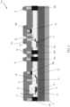
- FIG. 2 shows a HEMT with an enhancement mode gate and a depletion mode gate accordance with additional aspects of the present disclosure.
- the gate contact metal 26 to the field plate 22a may be replaced with a via contact 32a extending directly to the field plate 22a.
- the via contact 32a may extend through the interlevel dielectric materials 24, 30 and connect to the back end of the line metal wiring 38.
- a wiring structure e.g., gate wiring 38, may be directly connected to the field plate 22a, e.g., d-mode gate 21.
- the remaining features are similar to the structure 10 of FIG. 1 .
- FIG. 3 shows the field plate 22a that forms the d-mode gate 21, e.g., a metal-insulator-semiconductor (MIS) capacitor, electrically connected to the e-mode gate 19, e.g., pGaN islands.
- the field plate 22a may be electrically connected to the e-mode gate 19 by any combination of the metallization features 28, 32, 34 (where metallization feature 28 may be one of the ohmic contacts).
- the d-mode gate 21 and the e-mode gate 19 may be separately connected.
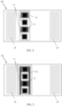
- FIGS. 4-6B show different layouts of the d-mode gate and the e-mode gate.
- the structure 10b includes d-mode gates 21 and e-mode gates 19 as separate islands under a single gate finger 50.
- the d-mode gates 21 and the e-mode gates 19 may be provided under multiple fingers.
- the spacing and sizing of the d-mode gates 21 and the e-mode gates 19 may be used to adjust the pinch off voltage.
- the ratios of the pGaN and d-mode gate widths may be adjusted to provide different Vt.
- the pGaN of the e-mode gates 19 will act to deplete the 2DEG concentration under the d-mode gate 21 to reduce the pinch off voltage.
- the structure 10c includes pGaN islands (e-mode gates 19) inside holes or openings 21a of the d-mode gate 21.
- the d-mode gate 21 surrounds the e-mode gate 19. This configuration will reduce high fields at the edges of the pGaN, e.g., of e-mode gate 19.
- the e-mode gate 19 may surround the d-mode gate 21 in a similar manner.
- FIG. 6A shows a top view of device with isolation regions and FIG. 6B is a cross-sectional view of the device of FIG. 6A along lines A-A.
- the structure 10d includes the d-mode gate 21 and the e-mode gate 19 surrounded by isolation regions 27.
- the isolation regions 27 may be formed in the semiconductor material 14 by an implantation process using, e.g., argon or nitrogen implants. In embodiments, other noble or inert gases may be used to form the isolation regions 27.
- the gate metal may be used to mask the device for the implant process.
- the isolation regions 27 may be self-aligned with the e-mode gate 19 and d-mode gate21, used to modulate and improve pinch off voltage. In further embodiments, the isolation regions 27 may also surround (isolate) the field plates 22, 22a.
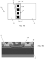
- the structure 10e shows the field plate 22a of the d-mode gate (e.g., MIS capacitor) overlapping with the e-mode gates 19.
- the d-mode gate e.g., MIS capacitor
- FIGS. 8A-8D show fabrication processes for manufacturing the structure shown in FIG. 1 in accordance with aspects of the present disclosure. It should be understood by those of ordinary skill in the art that similar fabrication processes may be used to manufacture the structure shown in FIGS. 2-7B .
- FIG. 8A shows a pGaN island (e.g., e-mode gate 19) formed on the semiconductor material 14 (e.g., conducting channel).
- the semiconductor material 14 may be deposited on the semiconductor substrate 12 using any conventional deposition method, e.g., CVD.
- semiconductor material 16 may be epitaxially grown on the semiconductor material 14.
- an in-situ doping e.g., p-type dopant
- Conductive material 18, e.g., TiN may be deposited on the semiconductor material 16.
- the semiconductor material 16 and conductive material 18 undergo conventional lithography and etching processes to form the e-mode gate 19, e.g., GaN island.
- the conductive material 18 may undergo an additional selective pull-back etching process to form the e-mode gate 19.
- a plurality of different materials 20 may be formed over the e-mode gate 19 and the semiconductor material 14.
- the plurality of different materials 20 may comprise, in sequential order, a conductive layer 20a, e.g., Al 2 O 3 , an etch stop layer 20b, e.g., SiN, and an insulator material 20c, e.g., SiO 2 .
- the plurality of different materials 20a, 20b, 20c may be deposited by conventional deposition methods, e.g., CVD processes, in sequential order.
- a trench 52 may be formed in the etch stop layer 20b and insulator material 20c, exposing the underlying conductive layer 20a.
- the trench 52 may be formed by conventional lithography and etching processes, with a selective chemistry to remove the etch stop layer 20b and insulator material 20c.
- corners of the trench 52 may be tapered or rounded using conventional etching processes which are known in the art such that no further explanation is required for a complete understanding of the present disclosure.
- the field plates 22, 22a may be formed in contact with the conductive layer 20a, e.g., Al 2 O 3 , and the insulator material 20c, e.g., SiO 2 .
- conductive material may be blanket deposited within the trenches 52 and insulator material 20c.
- the conductive material may be, e.g., TiN, deposited by a conventional deposition process, e.g., CVD. Following the deposition process, the conductive material may undergo a conventional etching process to form the field plates 22, 22a in contact with the underlying conductive layer 20a and over the insulator material 20c.
- Additional insulator material 24a e.g., interlevel dielectric material, may be formed over the field plates 22, 22a, which also fills in a remaining portion of the trench, as needed.
- additional interlevel dielectric material 24 may be deposited over the field plates 22, 22a.
- the gate contact metal 26, e.g., TiAl or TiN, may be formed in contact with the field plates 22, 22a and the conductive material 18, e.g., TiN, of the e-mode gate 19 using one or more conventional lithography, etching and deposition processes.
- a resist formed over the interlevel dielectric material 24 is exposed to energy (light) to form a pattern (opening).
- An etching process with a selective chemistry e.g., RIE, will be used to transfer the pattern from the photoresist layer to the interlevel dielectric material 24 to form one or more trenches in the interlevel dielectric material 24.
- conductive material can be deposited by any conventional deposition processes, e.g., chemical vapor deposition (CVD) processes. Any residual material on the surface of the interlevel dielectric material 24 can be removed by conventional chemical mechanical polishing (CMP) processes.
- CMP chemical mechanical polishing
- the gate contact metal 26 may be formed in several damascene processes, depending on the complexity of the shape of the gate contact metal 26.
- the ohmic contacts 28a-28f may also be formed in similar lithography, etching and deposition processes such that no further explanation is required herein for a complete understanding of the present disclosure.
- the interlevel dielectric material 30 may be formed over the interlevel dielectric material 24 using conventional deposition processes, e.g., CVD.
- the back end of the line contacts (e.g., metal vias) 32 and metal wiring 34, 36 may be formed by one or more conventional lithography, etching and deposition processes as already described herein.
- the HEMTs can be utilized in system on chip (SoC) technology.
- SoC is an integrated circuit (also known as a "chip") that integrates all components of an electronic system on a single chip or substrate. As the components are integrated on a single substrate, SoCs consume much less power and take up much less area than multichip designs with equivalent functionality. Because of this, SoCs are becoming the dominant force in the mobile computing (such as in Smartphones) and edge computing markets. SoC is also used in embedded systems and the Internet of Things.
- the method(s) as described above is used in the fabrication of integrated circuit chips.
- the resulting integrated circuit chips can be distributed by the fabricator in raw wafer form (that is, as a single wafer that has multiple unpackaged chips), as a bare die, or in a packaged form.
- the chip is mounted in a single chip package (such as a plastic carrier, with leads that are affixed to a motherboard or other higher level carrier) or in a multichip package (such as a ceramic carrier that has either or both surface interconnections or buried interconnections).
- the chip is then integrated with other chips, discrete circuit elements, and/or other signal processing devices as part of either (a) an intermediate product, such as a motherboard, or (b) an end product.
- the end product can be any product that includes integrated circuit chips, ranging from toys and other low-end applications to advanced computer products having a display, a keyboard or other input device, and a central processor.
Landscapes
- Junction Field-Effect Transistors (AREA)
- Thin Film Transistor (AREA)
- Insulated Gate Type Field-Effect Transistor (AREA)
- Engineering & Computer Science (AREA)
- Power Engineering (AREA)
Abstract
Description
- The present disclosure relates to semiconductor structures and, more particularly, to a high-electron-mobility transistor and methods of manufacture.
- A high-electron-mobility transistor (HEMT) is a field-effect transistor incorporating a junction between two materials with different band gaps (i.e. a heterojunction) as the channel, instead of a doped region (as is generally the case for a MOSFET). Commonly used material combinations are GaN or GaAs, although other materials can be used dependent on the application of the device.
- HEMT transistors are able to operate at higher frequencies than ordinary transistors, up to millimeter wave frequencies. As the HEMT transistors are able to operate at higher frequencies, they can be used in high-frequency products such as cell phones, satellite television receivers, voltage converters, and radar equipment. For example, a HEMT may be used in satellite receivers and in low power amplifiers.
- Depletion mode pinch off voltages in enhancement mode flows are typically higher than -6V; however, a layout programmable depletion mode pinch off of less than -6V is needed for GaN integrated circuit development, e.g., for building a low voltage reference, etc. Hence control of Vpinch becomes critical.
- In an aspect of the disclosure, a structure comprises: at least one depletion mode gate on a conductive material over a semiconductor material; and at least one enhancement mode gate electrically connected to the at least one depletion mode gate.
- Additional features of the structure are set forth in dependent claims 2 to 10. In an aspect of the disclosure, a structure comprises: a metal-insulator-semiconductor (MIS) capacitor, the MIS capacitor comprising a metal plate over a common conducting channel; and an island of semiconductor material over a semiconductor substrate and electrically connected to the MIS capacitor.
- Additional features of the structure are set forth in
dependent claims 12 to 14. In an aspect of the disclosure, a method comprises: forming at least one depletion mode gate comprising a field plate on a conductive material over a semiconductor material; and forming at least one enhancement mode gate electrically connected to the at least one depletion mode gate. - The present disclosure is described in the detailed description which follows, in reference to the noted plurality of drawings by way of non-limiting examples of exemplary embodiments of the present disclosure.
-
FIG. 1 shows a HEMT with an enhancement mode gate and a depletion mode gate and respective fabrication processes in accordance with aspects of the present disclosure. -
FIG. 2 shows a HEMT with an enhancement mode gate and a depletion mode gate in accordance with additional aspects of the present disclosure. -
FIG. 3 shows the enhancement mode gate electrically connected to the depletion mode gate in accordance with aspects of the present disclosure. -
FIGS. 4, 5 ,6A and 6B show several layouts of different HEMTs in accordance with aspects of the present disclosure. -
FIG. 7A shows a HEMT with an enhancement mode gate and a depletion mode gate in accordance with additional aspects of the present disclosure. -
FIG. 7B shows a cross-sectional view of the device ofFIG. 7A , along lines A-A. -
FIGS. 8A-8D show fabrication processes for manufacturing the structure shown inFIG. 1 in accordance with aspects of the present disclosure. - The present disclosure relates to semiconductor structures and, more particularly, to a high-electron-mobility transistor and methods of manufacture. More specifically, the present disclosure provides structures for depletion mode GaN HEMT Vt control. Advantageously, the present disclosure provides a dedicated depletion mode gate which provides significant improvement in gate control and subthreshold behavior. Also, no additional process complexity is required to generate multiple threshold depletion modes (d-modes).
- More specifically, the high-electron-mobility transistor (HEMT) may be a GaN HEMT with two gates, e.g., depletion mode gate and enhancement mode gate, connected together and, in embodiments, an isolation region (e.g., implant or shallow trench isolation structure)) placed between the two gates. The first gate metal (depletion mode gate) may be set for depletion mode operation and the second gate metal (enhancement mode gate) may be set for enhancement mode operation. In embodiments, the enhancement mode gate and the depletion mode gate may utilize field plates that are formed in a same deposition and patterning process. The depletion mode gate forms part of a metal-insulator-semiconductor (MIS) capacitor and the enhancement mode gate may be composed of an epitaxially grown p-type doped GaN layer. In embodiments, islands of the pGaN (enhancement mode gates) may be connected to MIS regions (depletion mode gate) by a common gate conductor. In alternative embodiments, the enhancement mode gate and the MIS region may be separately connected.
- The HEMTs of the present disclosure can be manufactured in a number of ways using a number of different tools. In general, though, the methodologies and tools are used to form structures with dimensions in the micrometer and nanometer scale. The methodologies, i.e., technologies, employed to manufacture the HEMTs of the present disclosure have been adopted from integrated circuit (IC) technology. For example, the structures are built on wafers and are realized in films of material patterned by photolithographic processes on the top of a wafer. In particular, the fabrication of the HEMTs uses three basic building blocks: (i) deposition of thin films of material on a substrate, (ii) applying a patterned mask on top of the films by photolithographic imaging, and (iii) etching the films selectively to the mask. In addition, precleaning processes may be used to clean etched surfaces of any contaminants, as is known in the art. Moreover, when necessary, rapid thermal anneal processes may be used to drive-in dopants or material layers as is known in the art.
-
FIG. 1 shows a HEMT with an enhancement mode gate and a depletion mode gate, and respective fabrication processes in accordance with aspects of the present disclosure. As in each of the embodiments, the enhancement mode gate and depletion mode gate may be integrated into a single wafer (substrate) with the depletion mode gate using a same field plate (as the gate) as the field plate for the enhancement mode gate. - More specifically, the structure of
FIG. 1 includes asemiconductor substrate 12 with asemiconductor material 14 on thesemiconductor substrate 12. Thesemiconductor material 14 may be AlGaN/GaN, which acts as a conducting channel for the HEMT device, e.g., enhancement mode gate (e-mode gate) and the depletion mode gate (d-mode gate). Thesemiconductor substrate 12 may be composed of any suitable material including, but not limited to, Si, SiGe, SiGeC, SiC, GaAs, InAs, InP, and other III/V or II/VI compound semiconductors. In preferred embodiments, thesemiconductor substrate 12 comprises p-type Si material with a suitable crystal orientation, e.g., (111). - A
semiconductor material 16 andconductive material 18 may be formed, e.g., deposited and patterned, on thesemiconductor material 14. In embodiments, thesemiconductor material 16 comprises, e.g., p-doped GaN, and theconductive material 18 may be, e.g., TiN. The combination of thesemiconductor material 16 and theconductive material 18 may be used as ane-mode gate 19. Thematerials conductive material 18 may be pulled back slightly as described inFIG. 8A . - Still referring to
FIG. 1 , a plurality ofdifferent materials 20 may be formed over thee-mode gate 19 andsemiconductor material 14. As described inFIG. 8B , the plurality ofdifferent materials 20 may comprise, in sequential order, a conductive layer, e.g., Al2O3, an etch stop layer, e.g., SiN, and an insulator material, e.g., SiO2. The plurality ofdifferent materials 20 may be deposited by conventional deposition methods, e.g., CVD processes, in sequential order to form layers of material over thee-mode gate 19 andsemiconductor material 14. -
Field plates different materials 20. In more specific embodiments, thefield plates FIG. 8C . Thefield plates e-mode gate 19 and d-mode gate 21. In embodiments, thefield plate 22a may form part of the d-mode gate 21, e.g., a metal-insulator-semiconductor (MIS) capacitor, which is electrically connected to the common conducting channel, e.g.,semiconductor material 14, through the conductive material of the plurality ofdifferent materials 18. Thefield plate 22 adjacent to thee-mode gate 19 may also be electrically connected to the common conducting channel, e.g.,semiconductor material 14, through the conductive material of the plurality ofdifferent materials 18. Moreover, thee-mode gate 19, e.g., pGaN islands, may be electrically connected to the d-mode gate 21 of the MIS gate structure as shown inFIGS. 3 and7 . - An interlevel
dielectric material 24, e.g., layers of oxide and nitride, may be formed over thefield plates gate contact metal 26 may be formed in contact with thefield plates conductive material 18, e.g., TiN, of thee-mode gate 19. Thegate contact metal 26 may be, e.g., TiAl or TiN. As described inFIG. 8D , thegate contact metal 26 may be formed by patterning of the interleveldielectric material 24 to expose theunderlying field plates conductive material 18, e.g., TiN of thee-mode gate 19, followed by deposition of conductive material, e.g., TiN. - As described in more detail with respect to
FIGS. 6A-6B ,isolation regions 27 may be formed in thesemiconductor material 14. In embodiments, theoptional isolation regions 27 may be an argon or nitrogen implant (or other inert or noble gas as is known in the art). More specifically, theoptional isolation regions 27 may be self-aligned with the e-mode gate, and may be used to isolate thee-mode gate 19, e.g., pGaN island, (and/or the d-mode gate 21 and/orfield plates pGaN islands 16 may also be used to deplete the 2DEG (e.g., 2-dimensionasl electron gas) in a gap between the gate metal stripes, e.g.,gate contact metal 26. In embodiments, thee-mode gate 19, e.g.,pGaN 16, and other structures may be shielded from the implant which forms theoptional isolation regions 27 by thegate contact metal 26. - Still referring to
FIG. 1 ,ohmic contacts ohmic contacts gate contact metal 26 of thee-mode gate 19 and the d-mode gate 21, respectively. An interlevel dielectric material 30 may be formed over the interleveldielectric material 24. Back end of the line contacts (e.g., metal vias) 32 may connect to theohmic contacts 28a-28f and thefield plates gate contact metal 26. In embodiments, theohmic contacts 28a-28f may be formed using conventional lithography, etching and deposition processes as is known in the art and further described inFIG. 8D . Theohmic contacts 28a-28f may comprise, e.g., TiAl or TiN. -
Metal wiring e-mode gate 19 and the d-mode gate 21. In embodiments, themetal wiring contacts 32. Themetal wiring -
FIG. 2 shows a HEMT with an enhancement mode gate and a depletion mode gate accordance with additional aspects of the present disclosure. In thestructure 10a ofFIG. 2 , thegate contact metal 26 to thefield plate 22a may be replaced with a viacontact 32a extending directly to thefield plate 22a. The viacontact 32a may extend through the interleveldielectric materials 24, 30 and connect to the back end of theline metal wiring 38. In this way, a wiring structure, e.g.,gate wiring 38, may be directly connected to thefield plate 22a, e.g., d-mode gate 21. The remaining features are similar to thestructure 10 ofFIG. 1 . -
FIG. 3 shows thefield plate 22a that forms the d-mode gate 21, e.g., a metal-insulator-semiconductor (MIS) capacitor, electrically connected to thee-mode gate 19, e.g., pGaN islands. In embodiments, thefield plate 22a may be electrically connected to thee-mode gate 19 by any combination of the metallization features 28, 32, 34 (wheremetallization feature 28 may be one of the ohmic contacts). In alternative embodiments, the d-mode gate 21 and thee-mode gate 19 may be separately connected. -
FIGS. 4-6B show different layouts of the d-mode gate and the e-mode gate. For example, inFIG. 4 thestructure 10b includes d-mode gates 21 ande-mode gates 19 as separate islands under asingle gate finger 50. It should be understood by those of ordinary skill in the art that the d-mode gates 21 and thee-mode gates 19 may be provided under multiple fingers. The spacing and sizing of the d-mode gates 21 and thee-mode gates 19 may be used to adjust the pinch off voltage. For example, the ratios of the pGaN and d-mode gate widths may be adjusted to provide different Vt. In this layout, the pGaN of thee-mode gates 19 will act to deplete the 2DEG concentration under the d-mode gate 21 to reduce the pinch off voltage. - In
FIG. 5 , thestructure 10c includes pGaN islands (e-mode gates 19) inside holes oropenings 21a of the d-mode gate 21. In this way, the d-mode gate 21 surrounds thee-mode gate 19. This configuration will reduce high fields at the edges of the pGaN, e.g., ofe-mode gate 19. In alternative embodiments, thee-mode gate 19 may surround the d-mode gate 21 in a similar manner. -
FIG. 6A shows a top view of device with isolation regions andFIG. 6B is a cross-sectional view of the device ofFIG. 6A along lines A-A. InFIGS. 6A and 6B , thestructure 10d includes the d-mode gate 21 and thee-mode gate 19 surrounded byisolation regions 27. In embodiments, theisolation regions 27 may be formed in thesemiconductor material 14 by an implantation process using, e.g., argon or nitrogen implants. In embodiments, other noble or inert gases may be used to form theisolation regions 27. In further embodiments, the gate metal may be used to mask the device for the implant process. Theisolation regions 27 may be self-aligned with thee-mode gate 19 and d-mode gate21, used to modulate and improve pinch off voltage. In further embodiments, theisolation regions 27 may also surround (isolate) thefield plates - In
FIGS. 7A and 7B , thestructure 10e shows thefield plate 22a of the d-mode gate (e.g., MIS capacitor) overlapping with thee-mode gates 19. -
FIGS. 8A-8D show fabrication processes for manufacturing the structure shown inFIG. 1 in accordance with aspects of the present disclosure. It should be understood by those of ordinary skill in the art that similar fabrication processes may be used to manufacture the structure shown inFIGS. 2-7B . -
FIG. 8A shows a pGaN island (e.g., e-mode gate 19) formed on the semiconductor material 14 (e.g., conducting channel). In embodiments, thesemiconductor material 14 may be deposited on thesemiconductor substrate 12 using any conventional deposition method, e.g., CVD. To form thee-mode gate 19,semiconductor material 16 may be epitaxially grown on thesemiconductor material 14. In embodiments, an in-situ doping (e.g., p-type dopant) may be used during the epitaxial growth process.Conductive material 18, e.g., TiN, may be deposited on thesemiconductor material 16. Thesemiconductor material 16 andconductive material 18 undergo conventional lithography and etching processes to form thee-mode gate 19, e.g., GaN island. In embodiments, theconductive material 18 may undergo an additional selective pull-back etching process to form thee-mode gate 19. - In
FIG. 8B , a plurality ofdifferent materials 20 may be formed over thee-mode gate 19 and thesemiconductor material 14. In embodiments, the plurality ofdifferent materials 20 may comprise, in sequential order, aconductive layer 20a, e.g., Al2O3, anetch stop layer 20b, e.g., SiN, and aninsulator material 20c, e.g., SiO2. The plurality ofdifferent materials - A
trench 52 may be formed in theetch stop layer 20b andinsulator material 20c, exposing the underlyingconductive layer 20a. Thetrench 52 may be formed by conventional lithography and etching processes, with a selective chemistry to remove theetch stop layer 20b andinsulator material 20c. In an optional embodiment, corners of thetrench 52 may be tapered or rounded using conventional etching processes which are known in the art such that no further explanation is required for a complete understanding of the present disclosure. - In
FIG. 8C , thefield plates conductive layer 20a, e.g., Al2O3, and theinsulator material 20c, e.g., SiO2. In more specific embodiments, conductive material may be blanket deposited within thetrenches 52 andinsulator material 20c. The conductive material may be, e.g., TiN, deposited by a conventional deposition process, e.g., CVD. Following the deposition process, the conductive material may undergo a conventional etching process to form thefield plates conductive layer 20a and over theinsulator material 20c.Additional insulator material 24a, e.g., interlevel dielectric material, may be formed over thefield plates - As further shown in
FIG. 8D , additional interleveldielectric material 24 may be deposited over thefield plates gate contact metal 26, e.g., TiAl or TiN, may be formed in contact with thefield plates conductive material 18, e.g., TiN, of thee-mode gate 19 using one or more conventional lithography, etching and deposition processes. - By way of example, a resist formed over the interlevel
dielectric material 24 is exposed to energy (light) to form a pattern (opening). An etching process with a selective chemistry, e.g., RIE, will be used to transfer the pattern from the photoresist layer to the interleveldielectric material 24 to form one or more trenches in the interleveldielectric material 24. Following the resist removal by a conventional oxygen ashing process or other known stripants, conductive material can be deposited by any conventional deposition processes, e.g., chemical vapor deposition (CVD) processes. Any residual material on the surface of the interleveldielectric material 24 can be removed by conventional chemical mechanical polishing (CMP) processes. - It should be understood by those of ordinary skill in the art that the
gate contact metal 26 may be formed in several damascene processes, depending on the complexity of the shape of thegate contact metal 26. Theohmic contacts 28a-28f may also be formed in similar lithography, etching and deposition processes such that no further explanation is required herein for a complete understanding of the present disclosure. - Referring back to
FIG. 1 , the interlevel dielectric material 30 may be formed over the interleveldielectric material 24 using conventional deposition processes, e.g., CVD. The back end of the line contacts (e.g., metal vias) 32 andmetal wiring - The HEMTs can be utilized in system on chip (SoC) technology. The SoC is an integrated circuit (also known as a "chip") that integrates all components of an electronic system on a single chip or substrate. As the components are integrated on a single substrate, SoCs consume much less power and take up much less area than multichip designs with equivalent functionality. Because of this, SoCs are becoming the dominant force in the mobile computing (such as in Smartphones) and edge computing markets. SoC is also used in embedded systems and the Internet of Things.
- The method(s) as described above is used in the fabrication of integrated circuit chips. The resulting integrated circuit chips can be distributed by the fabricator in raw wafer form (that is, as a single wafer that has multiple unpackaged chips), as a bare die, or in a packaged form. In the latter case the chip is mounted in a single chip package (such as a plastic carrier, with leads that are affixed to a motherboard or other higher level carrier) or in a multichip package (such as a ceramic carrier that has either or both surface interconnections or buried interconnections). In any case the chip is then integrated with other chips, discrete circuit elements, and/or other signal processing devices as part of either (a) an intermediate product, such as a motherboard, or (b) an end product. The end product can be any product that includes integrated circuit chips, ranging from toys and other low-end applications to advanced computer products having a display, a keyboard or other input device, and a central processor.
- The descriptions of the various embodiments of the present disclosure have been presented for purposes of illustration, but are not intended to be exhaustive or limited to the embodiments disclosed. Many modifications and variations will be apparent to those of ordinary skill in the art without departing from the scope and spirit of the described embodiments. The terminology used herein was chosen to best explain the principles of the embodiments, the practical application or technical improvement over technologies found in the marketplace, or to enable others of ordinary skill in the art to understand the embodiments disclosed herein.
Claims (15)
- A structure comprising:at least one depletion mode gate on a conductive material over a semiconductor material; andat least one enhancement mode gate electrically connected to the at least one depletion mode gate and over the semiconductor material.
- The structure of claim 1, wherein the at least one enhancement mode gate comprises a GaN island with a gate metal connecting to the GaN island.
- The structure of claim 2, further comprising an intervening conductive material between the GaN island and the gate metal connecting to the GaN island.
- The structure of claim 2 or claim 3, wherein the GaN island is a p-doped GaN island.
- The structure of claim 1, wherein the at least one depletion mode gate comprises a field plate, and, optionally, wherein the at least one depletion mode gate comprises a metal insulator semiconductor (MIS) capacitor.
- The structure of claim 5, wherein the semiconductor material comprises a common conducting channel of the at least one depletion mode gate and the least one enhancement mode gate, and the field plate of the at least one depletion mode gate forms part of the MIS capacitor, and, optionally, wherein the common conducting channel comprises GaN.
- The structure of one of claims 1 to 6, wherein the at least one depletion mode gate and the least one enhancement mode gate comprise alternating islands of pGaN and MIS gate structures under a single gate metal finger.
- The structure of one of claims 1 to 6, wherein the at least one depletion mode gate surrounds the at least one enhancement mode gate.
- The structure of one of claims 1 to 8, further comprising isolation regions in the semiconductor material, the isolation regions surrounding the least one enhancement mode gate and the at least one depletion mode gate, and, optionally, wherein the isolation regions surround field plates of the at least one depletion mode gate.
- The structure of one of claims 1 to 9, wherein a field plate comprising the at least one depletion mode gate overlaps with the at least one enhancement mode gate.
- A structure comprising:a metal-insulator-semiconductor (MIS) capacitor, the MIS capacitor comprising a metal plate over a common conducting channel; andan island of semiconductor material over a semiconductor substrate and electrically connected to the MIS capacitor.
- The structure of claim 11, wherein the common conducting channel comprises GaN.
- The structure of claim 11 or claim 12, further comprising isolation regions surrounding the MIS capacitor and the island of semiconductor material, and, optionally, wherein the island of semiconductor material comprises pGaN.
- The structure of one of claims 11 to 13, wherein the metal plate of the MIS capacitor overlaps with the island of semiconductor material and/or wherein the island of semiconductor material comprises an enhancement mode gate.
- A method comprising:forming at least one depletion mode gate comprising a field plate on a conductive material over a semiconductor material; andforming at least one enhancement mode gate electrically connected to the at least one depletion mode gate and over the semiconductor material.
Applications Claiming Priority (1)
| Application Number | Priority Date | Filing Date | Title |
|---|---|---|---|
| US17/902,463 US20240079405A1 (en) | 2022-09-02 | 2022-09-02 | High-electron-mobility transistor |
Publications (2)
| Publication Number | Publication Date |
|---|---|
| EP4333042A2 true EP4333042A2 (en) | 2024-03-06 |
| EP4333042A3 EP4333042A3 (en) | 2024-07-17 |
Family
ID=87418780
Family Applications (1)
| Application Number | Title | Priority Date | Filing Date |
|---|---|---|---|
| EP23186269.9A Pending EP4333042A3 (en) | 2022-09-02 | 2023-07-19 | High-electron-mobility transistor |
Country Status (3)
| Country | Link |
|---|---|
| US (1) | US20240079405A1 (en) |
| EP (1) | EP4333042A3 (en) |
| CN (1) | CN117650170A (en) |
Family Cites Families (7)
| Publication number | Priority date | Publication date | Assignee | Title |
|---|---|---|---|---|
| JP6161910B2 (en) * | 2013-01-30 | 2017-07-12 | ルネサスエレクトロニクス株式会社 | Semiconductor device |
| US9633920B2 (en) * | 2015-02-12 | 2017-04-25 | Taiwan Semiconductor Manufacturing Co., Ltd. | Low damage passivation layer for III-V based devices |
| DE102015118440A1 (en) * | 2015-10-28 | 2017-05-04 | Infineon Technologies Austria Ag | Semiconductor device |
| JP7300840B2 (en) * | 2019-02-04 | 2023-06-30 | ローム株式会社 | Manufacturing method of nitride semiconductor device |
| US11658236B2 (en) * | 2019-05-07 | 2023-05-23 | Cambridge Gan Devices Limited | III-V semiconductor device with integrated power transistor and start-up circuit |
| TWI749369B (en) * | 2019-09-12 | 2021-12-11 | 黃知澍 | N-face III/nitride epitaxial structure and its active device and its gate protection device |
| CN114823888B (en) * | 2021-01-22 | 2025-10-03 | 联华电子股份有限公司 | High electron mobility transistor and manufacturing method thereof |
-
2022
- 2022-09-02 US US17/902,463 patent/US20240079405A1/en active Pending
-
2023
- 2023-07-19 EP EP23186269.9A patent/EP4333042A3/en active Pending
- 2023-08-14 CN CN202311017723.8A patent/CN117650170A/en active Pending
Also Published As
| Publication number | Publication date |
|---|---|
| CN117650170A (en) | 2024-03-05 |
| EP4333042A3 (en) | 2024-07-17 |
| US20240079405A1 (en) | 2024-03-07 |
Similar Documents
| Publication | Publication Date | Title |
|---|---|---|
| US20240194680A1 (en) | Bidirectional device | |
| US12142686B2 (en) | Field effect transistor | |
| EP4379811A2 (en) | High-electron-mobility transistor | |
| EP4354511A2 (en) | Device with field plates | |
| CN119947165A (en) | High electron mobility transistor with regenerative barrier | |
| US20240079405A1 (en) | High-electron-mobility transistor | |
| EP4535429A1 (en) | High-electron-mobility transistor | |
| US12538550B2 (en) | High-electron-mobility transistor with field plate and sidewall spacers | |
| US20250072024A1 (en) | Transistor with thermal plug | |
| EP4597577A1 (en) | Device with outer conductive spacer | |
| US12550410B2 (en) | High electron mobility transistors | |
| US12581701B2 (en) | Device with dual isolation structure | |
| EP4597578A1 (en) | Device with inner and outer spacers | |
| US20260143778A1 (en) | Body contacted transistors | |
| EP4550395A1 (en) | Device with isolation structures | |
| EP4539125A1 (en) | High electron mobility transistor | |
| US20250040221A1 (en) | High-electron-mobility transistor | |
| EP4597576A1 (en) | Device with inner spacer sidewall structures | |
| US11605649B2 (en) | Switches in bulk substrate |
Legal Events
| Date | Code | Title | Description |
|---|---|---|---|
| PUAI | Public reference made under article 153(3) epc to a published international application that has entered the european phase |
Free format text: ORIGINAL CODE: 0009012 |
|
| STAA | Information on the status of an ep patent application or granted ep patent |
Free format text: STATUS: THE APPLICATION HAS BEEN PUBLISHED |
|
| AK | Designated contracting states |
Kind code of ref document: A2 Designated state(s): AL AT BE BG CH CY CZ DE DK EE ES FI FR GB GR HR HU IE IS IT LI LT LU LV MC ME MK MT NL NO PL PT RO RS SE SI SK SM TR |
|
| RIC1 | Information provided on ipc code assigned before grant |
Ipc: H01L 29/778 20060101ALI20240426BHEP Ipc: H01L 29/40 20060101ALI20240426BHEP Ipc: H01L 29/20 20060101ALI20240426BHEP Ipc: H01L 29/10 20060101ALI20240426BHEP Ipc: H01L 27/085 20060101ALI20240426BHEP Ipc: H01L 27/06 20060101ALI20240426BHEP Ipc: H01L 21/8252 20060101AFI20240426BHEP |
|
| PUAL | Search report despatched |
Free format text: ORIGINAL CODE: 0009013 |
|
| AK | Designated contracting states |
Kind code of ref document: A3 Designated state(s): AL AT BE BG CH CY CZ DE DK EE ES FI FR GB GR HR HU IE IS IT LI LT LU LV MC ME MK MT NL NO PL PT RO RS SE SI SK SM TR |
|
| RIC1 | Information provided on ipc code assigned before grant |
Ipc: H01L 29/66 20060101ALI20240611BHEP Ipc: H01L 29/778 20060101ALI20240611BHEP Ipc: H01L 29/40 20060101ALI20240611BHEP Ipc: H01L 29/20 20060101ALI20240611BHEP Ipc: H01L 29/10 20060101ALI20240611BHEP Ipc: H01L 27/085 20060101ALI20240611BHEP Ipc: H01L 27/06 20060101ALI20240611BHEP Ipc: H01L 21/8252 20060101AFI20240611BHEP |
|
| STAA | Information on the status of an ep patent application or granted ep patent |
Free format text: STATUS: REQUEST FOR EXAMINATION WAS MADE |
|
| 17P | Request for examination filed |
Effective date: 20241204 |
|
| RBV | Designated contracting states (corrected) |
Designated state(s): AL AT BE BG CH CY CZ DE DK EE ES FI FR GB GR HR HU IE IS IT LI LT LU LV MC ME MK MT NL NO PL PT RO RS SE SI SK SM TR |