EP4329101A1 - Radio wave absorbing element and assembly - Google Patents
Radio wave absorbing element and assembly Download PDFInfo
- Publication number
- EP4329101A1 EP4329101A1 EP21937974.0A EP21937974A EP4329101A1 EP 4329101 A1 EP4329101 A1 EP 4329101A1 EP 21937974 A EP21937974 A EP 21937974A EP 4329101 A1 EP4329101 A1 EP 4329101A1
- Authority
- EP
- European Patent Office
- Prior art keywords
- resonator
- conductor
- radio wave
- plane
- plane direction
- Prior art date
- Legal status (The legal status is an assumption and is not a legal conclusion. Google has not performed a legal analysis and makes no representation as to the accuracy of the status listed.)
- Withdrawn
Links
Images


Classifications
-
- H—ELECTRICITY
- H01—ELECTRIC ELEMENTS
- H01Q—ANTENNAS, i.e. RADIO AERIALS
- H01Q17/00—Devices for absorbing waves radiated from an antenna; Combinations of such devices with active antenna elements or systems
-
- H—ELECTRICITY
- H01—ELECTRIC ELEMENTS
- H01Q—ANTENNAS, i.e. RADIO AERIALS
- H01Q1/00—Details of, or arrangements associated with, antennas
- H01Q1/52—Means for reducing coupling between antennas; Means for reducing coupling between an antenna and another structure
- H01Q1/526—Electromagnetic shields
-
- H—ELECTRICITY
- H01—ELECTRIC ELEMENTS
- H01Q—ANTENNAS, i.e. RADIO AERIALS
- H01Q13/00—Waveguide horns or mouths; Slot antennas; Leaky-waveguide antennas; Equivalent structures causing radiation along the transmission path of a guided wave
- H01Q13/08—Radiating ends of two-conductor microwave transmission lines, e.g. of coaxial lines, of microstrip lines
-
- H—ELECTRICITY
- H01—ELECTRIC ELEMENTS
- H01Q—ANTENNAS, i.e. RADIO AERIALS
- H01Q15/00—Devices for reflection, refraction, diffraction or polarisation of waves radiated from an antenna, e.g. quasi-optical devices
- H01Q15/14—Reflecting surfaces; Equivalent structures
-
- H—ELECTRICITY
- H01—ELECTRIC ELEMENTS
- H01Q—ANTENNAS, i.e. RADIO AERIALS
- H01Q21/00—Antenna arrays or systems
- H01Q21/06—Arrays of individually energised antenna units similarly polarised and spaced apart
- H01Q21/061—Two dimensional planar arrays
- H01Q21/065—Patch antenna array
-
- H—ELECTRICITY
- H01—ELECTRIC ELEMENTS
- H01Q—ANTENNAS, i.e. RADIO AERIALS
- H01Q25/00—Antennas or antenna systems providing at least two radiating patterns
- H01Q25/005—Antennas or antenna systems providing at least two radiating patterns providing two patterns of opposite direction; back to back antennas
-
- H—ELECTRICITY
- H01—ELECTRIC ELEMENTS
- H01Q—ANTENNAS, i.e. RADIO AERIALS
- H01Q9/00—Electrically-short antennas having dimensions not more than twice the operating wavelength and consisting of conductive active radiating elements
- H01Q9/04—Resonant antennas
- H01Q9/0407—Substantially flat resonant element parallel to ground plane, e.g. patch antenna
- H01Q9/0414—Substantially flat resonant element parallel to ground plane, e.g. patch antenna in a stacked or folded configuration
Definitions
- the present disclosure relates to a radio wave absorbing element and an assembly.
- Patent Document 1 describes a technique of absorbing radio waves in a structure including an array of resonator elements.
- Patent Document 1 JP 61-88591 A
- the resonator element described in Patent Document 1 includes an impedance conversion layer and thus has a problem of having a large thickness.
- the present disclosure provides a radio wave absorbing element and an assembly configured to shield electromagnetic waves in a predetermined frequency band.
- a radio wave absorbing element includes a first resonator extending in a first plane direction, a second resonator spaced apart from the first resonator in a first direction and extending in the first plane direction, a third resonator located between the first resonator and the second resonator in the first direction and configured to magnetically or capacitively connect to or electrically connect to each of the first resonator and the second resonator, a reference conductor extending in the first plane direction, located between the first resonator and the second resonator in the first direction, and serving as a potential reference of the first resonator and the second resonator, and a shielding conductor spaced apart from the second resonator in the first direction and extending in the first plane direction, in which the reference conductor surrounds at least a part of the third resonator in the first plane direction.
- An assembly according to the present disclosure includes a plurality of the radio wave absorbing elements according to the present disclosure, and the plurality of radio wave absorbing elements are arranged in the first plane direction.
- electromagnetic waves in a predetermined frequency band can be shielded.
- an XYZ orthogonal coordinate system is set, and the positional relationship between respective portions will be described by referring to the XYZ orthogonal coordinate system.
- a direction parallel to an X-axis in a horizontal plane is defined as an X-axis direction
- a direction parallel to a Y-axis orthogonal to the X-axis in the horizontal plane is defined as a Y-axis direction
- a direction parallel to a Z-axis orthogonal to the horizontal plane is defined as a Z-axis direction.
- a plane including the X-axis and the Y-axis is appropriately referred to as an XY plane
- a plane including the X-axis and the Z-axis is appropriately referred to as an XZ plane
- a plane including the Y-axis and the Z-axis is appropriately referred to as a YZ plane.
- the XY plane is parallel to the horizontal plane.
- the XY plane, the XZ plane, and the YZ plane are orthogonal to each other.
- FIG. 1 illustrates an assembly in which a plurality of unit structures are periodically arranged.
- the plurality of unit structures periodically arranged function as an assembly.
- the assembly can function as a radio wave absorbing plate shielding radio waves in a predetermined frequency band.
- an assembly 1 includes a plurality of unit structures 10 and a substrate 12.
- the plurality of unit structures 10 are arranged in an XY plane direction.
- the XY plane direction may also be referred to as a first plane direction. That is, the plurality of unit structures 10 are arranged two-dimensionally.
- Each of the plurality of unit structures 10 has a structure shielding the radio waves.
- the structure of the unit structure 10 will be described later.
- the unit structure 10 may be referred to as a radio wave absorbing element.
- the substrate 12 may be, for example, a dielectric substrate made of a dielectric body.
- the assembly 1 is made by two-dimensionally arranging the plurality of unit structures 10 on the substrate 12 made of the dielectric body.
- the assembly can be configured by arranging the unit structures of the following embodiment as illustrated in FIG. 1 .
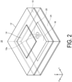
- FIG. 2 is a diagram illustrating the configuration of the unit structure according to the embodiment.
- the unit structure 10 includes the substrate 12, a first resonator 14, a second resonator 16, a reference conductor 18, a connection line path 20, and a shielding conductor 24.
- the first resonator 14 may be arranged on the substrate 12, extending on the XY plane.
- the first resonator 14 may be made of a conductor.
- the first resonator 14 may be, for example, a patch conductor formed in a rectangular shape. In the example illustrated in FIG. 2 , the first resonator 14 is illustrated as the rectangular patch conductor, but the present disclosure is not limited thereto.
- the first resonator 14 may have, for example, a linear shape, a circular shape, a loop shape, or a polygonal shape other than a rectangular shape. That is, the shape of the first resonator 14 may be arbitrarily changed according to the design.
- the first resonator 14 resonates by an electromagnetic wave received from the +Z-axis direction.
- the first resonator 14 radiates an electromagnetic wave during resonance.
- the first resonator 14 radiates the electromagnetic wave to the +Z-axis direction side during resonance.
- the second resonator 16 may be arranged on the substrate 12 to extend on the XY plane at a position away from the first resonator 14 in the Z-axis direction.
- the second resonator 16 may be, for example, a patch conductor formed in a rectangular shape. In the example illustrated in FIG. 2 , the second resonator 16 is illustrated as the rectangular patch conductor, but the present disclosure is not limited thereto.
- the second resonator 16 may have, for example, a linear shape, a circular shape, a loop shape, or a polygonal shape other than a rectangular shape. That is, the shape of the second resonator 16 may be arbitrarily changed according to the design.
- the shape of the second resonator 16 may be the same as or different from the shape of the first resonator 14.
- the area of the second resonator 16 may be the same as or different from the area of the first resonator 14.
- the second resonator 16 radiates an electromagnetic wave during resonance.
- the second resonator 16 for example, radiates the electromagnetic wave to the -Z-axis direction side.
- the second resonator 16 radiates the electromagnetic wave to the -Z-axis direction side during resonance.
- the second resonator 16 resonates by receiving the electromagnetic wave from the -Z-axis direction.
- the second resonator 16 may resonate at a phase different from that of the first resonator 14.
- the second resonator 16 may resonate in a direction different from the first resonator 14 in the XY plane direction.
- the second resonator 16 may resonate in the Y-axis direction.
- the resonance direction of the second resonator 16 may change with time in the XY plane direction corresponding to a change with time in the resonance direction of the first resonator 14.
- the second resonator 16 may radiate the electromagnetic wave received by the first resonator 14 with a first frequency band thereof attenuated.
- the reference conductor 18 may be arranged between the first resonator 14 and the second resonator 16 in the substrate 12.
- the reference conductor 18 may be, for example, at the center between the first resonator 14 and the second resonator 16 in the substrate 12, but the present disclosure is not limited thereto.
- the reference conductor 18 may be at a position where the distance from the reference conductor 18 to the first resonator 14 differs from the distance from the reference conductor 18 to the second resonator 16.
- the reference conductor 18 has a through-hole 18a through which the connection line path 20 extends.
- the reference conductor 18 surrounds at least a part of the connection line path 20.
- the connection line path 20 may be made of a conductor.
- the connection line path 20 is located between the first resonator 14 and the second resonator 16 in the Z-axis direction.
- the Z-axis direction may also be referred to as a first direction, for example.
- the connection line path 20 may be connected to each of the first resonator 14 and the second resonator 16. Although the connection line path 20 passes through the through-hole 18a, the connection line path 20 is not in contact with the reference conductor 18.
- the connection line path 20 may be magnetically or capacitively connected to each of the first resonator 14 and the second resonator 16, for example.
- the connection line path 20 may be electrically connected to each of the first resonator 14 and the second resonator 16.
- connection line path 20 is connected to a side of the first resonator 14 parallel to the X-axis direction and is connected to a side of the second resonator 16 parallel to the X-axis direction.
- the connection line path 20 may be a path parallel to the Z-axis direction.
- the connection line path 20 may be a third resonator.
- the shielding conductor 24 is made of a conductor.
- the shielding conductor 24 is arranged below the second resonator 16 in the Z-axis direction.
- the shielding conductor 24 is arranged to receive the electromagnetic wave radiated from the second resonator 16.
- the shielding conductor 24 is arranged such that the electromagnetic wave incident on the first resonator 14 is not radiated from the unit structure 10. In other words, the shielding conductor 24 shields the electromagnetic wave received by the first resonator 14.
- the shielding conductor 24 shields the electromagnetic wave radiated by the second resonator 16.
- FIG. 3 is a graph showing the frequency characteristics of the unit structure according to the embodiment.
- FIG. 3 shows a graph G1.
- the graph G1 shows a reflection coefficient.
- the unit structure 10 has an insertion loss of -2.50 dB or more in a range from around 18.00 GHz to around 28.00 GHz.
- the unit structure 10 has an insertion loss of -17.50 dB or less in a range around 21.50 GHz.
- the unit structure 10 does not transmit the electromagnetic wave in a frequency band around 21.50 GHz. That is, the unit structure 10 does not transmit the electromagnetic wave in a specific frequency band.
- the unit structure 10 can shield the electromagnetic wave at the specific frequency. The frequency to be shielded against can be changed according to the resonant frequency of the unit structure 10.
Landscapes
- Physics & Mathematics (AREA)
- Electromagnetism (AREA)
- Shielding Devices Or Components To Electric Or Magnetic Fields (AREA)
- Aerials With Secondary Devices (AREA)
- Waveguide Aerials (AREA)
Abstract
Description
- The present disclosure relates to a radio wave absorbing element and an assembly.
- A known technique involves controlling electromagnetic waves without using a dielectric lens. For example,
Patent Document 1 describes a technique of absorbing radio waves in a structure including an array of resonator elements. - Patent Document 1:
JP 61-88591 A - The resonator element described in
Patent Document 1 includes an impedance conversion layer and thus has a problem of having a large thickness. - The present disclosure provides a radio wave absorbing element and an assembly configured to shield electromagnetic waves in a predetermined frequency band.
- A radio wave absorbing element according the present disclosure includes a first resonator extending in a first plane direction, a second resonator spaced apart from the first resonator in a first direction and extending in the first plane direction, a third resonator located between the first resonator and the second resonator in the first direction and configured to magnetically or capacitively connect to or electrically connect to each of the first resonator and the second resonator, a reference conductor extending in the first plane direction, located between the first resonator and the second resonator in the first direction, and serving as a potential reference of the first resonator and the second resonator, and a shielding conductor spaced apart from the second resonator in the first direction and extending in the first plane direction, in which the reference conductor surrounds at least a part of the third resonator in the first plane direction.
- An assembly according to the present disclosure includes a plurality of the radio wave absorbing elements according to the present disclosure, and the plurality of radio wave absorbing elements are arranged in the first plane direction.
- According to the present disclosure, electromagnetic waves in a predetermined frequency band can be shielded.
-
-
FIG. 1 is a diagram illustrating an overview of an assembly according to an embodiment. -
FIG. 2 is a diagram schematically illustrating a configuration of a unit structure according to the embodiment. -
FIG. 3 is a graph showing frequency characteristics of the unit structure according to the embodiment. - Embodiments of the present disclosure will be described in detail with reference to the drawings. The embodiments described below do not limit the present disclosure.
- In the following description, an XYZ orthogonal coordinate system is set, and the positional relationship between respective portions will be described by referring to the XYZ orthogonal coordinate system. A direction parallel to an X-axis in a horizontal plane is defined as an X-axis direction, a direction parallel to a Y-axis orthogonal to the X-axis in the horizontal plane is defined as a Y-axis direction, and a direction parallel to a Z-axis orthogonal to the horizontal plane is defined as a Z-axis direction. A plane including the X-axis and the Y-axis is appropriately referred to as an XY plane, a plane including the X-axis and the Z-axis is appropriately referred to as an XZ plane, and a plane including the Y-axis and the Z-axis is appropriately referred to as a YZ plane. The XY plane is parallel to the horizontal plane. The XY plane, the XZ plane, and the YZ plane are orthogonal to each other.
-
FIG. 1 illustrates an assembly in which a plurality of unit structures are periodically arranged. In the assembly, the plurality of unit structures periodically arranged function as an assembly. For example, the assembly can function as a radio wave absorbing plate shielding radio waves in a predetermined frequency band. - As illustrated in
FIG. 1 , anassembly 1 includes a plurality ofunit structures 10 and asubstrate 12. - The plurality of
unit structures 10 are arranged in an XY plane direction. The XY plane direction may also be referred to as a first plane direction. That is, the plurality ofunit structures 10 are arranged two-dimensionally. Each of the plurality ofunit structures 10 has a structure shielding the radio waves. The structure of theunit structure 10 will be described later. Theunit structure 10 may be referred to as a radio wave absorbing element. Thesubstrate 12 may be, for example, a dielectric substrate made of a dielectric body. Theassembly 1 is made by two-dimensionally arranging the plurality ofunit structures 10 on thesubstrate 12 made of the dielectric body. - In the present disclosure, the assembly can be configured by arranging the unit structures of the following embodiment as illustrated in
FIG. 1 . - A configuration of the unit structure according to the embodiment will be described with reference to
FIG. 2. FIG. 2 is a diagram illustrating the configuration of the unit structure according to the embodiment. - As illustrated in
FIG. 2 , theunit structure 10 includes thesubstrate 12, afirst resonator 14, asecond resonator 16, areference conductor 18, aconnection line path 20, and ashielding conductor 24. - The
first resonator 14 may be arranged on thesubstrate 12, extending on the XY plane. Thefirst resonator 14 may be made of a conductor. Thefirst resonator 14 may be, for example, a patch conductor formed in a rectangular shape. In the example illustrated inFIG. 2 , thefirst resonator 14 is illustrated as the rectangular patch conductor, but the present disclosure is not limited thereto. Thefirst resonator 14 may have, for example, a linear shape, a circular shape, a loop shape, or a polygonal shape other than a rectangular shape. That is, the shape of thefirst resonator 14 may be arbitrarily changed according to the design. Thefirst resonator 14 resonates by an electromagnetic wave received from the +Z-axis direction. - The
first resonator 14 radiates an electromagnetic wave during resonance. Thefirst resonator 14 radiates the electromagnetic wave to the +Z-axis direction side during resonance. - The
second resonator 16 may be arranged on thesubstrate 12 to extend on the XY plane at a position away from thefirst resonator 14 in the Z-axis direction. Thesecond resonator 16 may be, for example, a patch conductor formed in a rectangular shape. In the example illustrated inFIG. 2 , thesecond resonator 16 is illustrated as the rectangular patch conductor, but the present disclosure is not limited thereto. Thesecond resonator 16 may have, for example, a linear shape, a circular shape, a loop shape, or a polygonal shape other than a rectangular shape. That is, the shape of thesecond resonator 16 may be arbitrarily changed according to the design. The shape of thesecond resonator 16 may be the same as or different from the shape of thefirst resonator 14. The area of thesecond resonator 16 may be the same as or different from the area of thefirst resonator 14. - The
second resonator 16 radiates an electromagnetic wave during resonance. Thesecond resonator 16, for example, radiates the electromagnetic wave to the -Z-axis direction side. Thesecond resonator 16 radiates the electromagnetic wave to the -Z-axis direction side during resonance. Thesecond resonator 16 resonates by receiving the electromagnetic wave from the -Z-axis direction. - The
second resonator 16 may resonate at a phase different from that of thefirst resonator 14. Thesecond resonator 16 may resonate in a direction different from thefirst resonator 14 in the XY plane direction. For example, when thefirst resonator 14 resonates in the X-axis direction, thesecond resonator 16 may resonate in the Y-axis direction. The resonance direction of thesecond resonator 16 may change with time in the XY plane direction corresponding to a change with time in the resonance direction of thefirst resonator 14. Thesecond resonator 16 may radiate the electromagnetic wave received by thefirst resonator 14 with a first frequency band thereof attenuated. - The
reference conductor 18 may be arranged between thefirst resonator 14 and thesecond resonator 16 in thesubstrate 12. Thereference conductor 18 may be, for example, at the center between thefirst resonator 14 and thesecond resonator 16 in thesubstrate 12, but the present disclosure is not limited thereto. For example, thereference conductor 18 may be at a position where the distance from thereference conductor 18 to thefirst resonator 14 differs from the distance from thereference conductor 18 to thesecond resonator 16. Thereference conductor 18 has a through-hole 18a through which theconnection line path 20 extends. Thereference conductor 18 surrounds at least a part of theconnection line path 20. - The
connection line path 20 may be made of a conductor. Theconnection line path 20 is located between thefirst resonator 14 and thesecond resonator 16 in the Z-axis direction. The Z-axis direction may also be referred to as a first direction, for example. Theconnection line path 20 may be connected to each of thefirst resonator 14 and thesecond resonator 16. Although theconnection line path 20 passes through the through-hole 18a, theconnection line path 20 is not in contact with thereference conductor 18. Theconnection line path 20 may be magnetically or capacitively connected to each of thefirst resonator 14 and thesecond resonator 16, for example. For example, theconnection line path 20 may be electrically connected to each of thefirst resonator 14 and thesecond resonator 16. Theconnection line path 20 is connected to a side of thefirst resonator 14 parallel to the X-axis direction and is connected to a side of thesecond resonator 16 parallel to the X-axis direction. Theconnection line path 20 may be a path parallel to the Z-axis direction. Theconnection line path 20 may be a third resonator. - The shielding
conductor 24 is made of a conductor. The shieldingconductor 24 is arranged below thesecond resonator 16 in the Z-axis direction. The shieldingconductor 24 is arranged to receive the electromagnetic wave radiated from thesecond resonator 16. The shieldingconductor 24 is arranged such that the electromagnetic wave incident on thefirst resonator 14 is not radiated from theunit structure 10. In other words, the shieldingconductor 24 shields the electromagnetic wave received by thefirst resonator 14. The shieldingconductor 24 shields the electromagnetic wave radiated by thesecond resonator 16. - Frequency characteristics of the unit structure according to the embodiment will be described with reference to
FIG. 3. FIG. 3 is a graph showing the frequency characteristics of the unit structure according to the embodiment. - In
FIG. 3 , the horizontal axis represents the frequency [Giga Hertz (GHz)] and the vertical axis represents the gain [deci Bel (dB)].FIG. 3 shows a graph G1. The graph G1 shows a reflection coefficient. As shown in graph G1, theunit structure 10 has an insertion loss of -2.50 dB or more in a range from around 18.00 GHz to around 28.00 GHz. Theunit structure 10 has an insertion loss of -17.50 dB or less in a range around 21.50 GHz. Theunit structure 10 does not transmit the electromagnetic wave in a frequency band around 21.50 GHz. That is, theunit structure 10 does not transmit the electromagnetic wave in a specific frequency band. Theunit structure 10 can shield the electromagnetic wave at the specific frequency. The frequency to be shielded against can be changed according to the resonant frequency of theunit structure 10. - Embodiments of the present disclosure have been described above, but the present disclosure is not limited by the contents of the embodiments. Constituent elements described above include those that can be easily assumed by a person skilled in the art, those that are substantially identical to the constituent elements, and those within a so-called range of equivalency. The constituent elements described above can be combined as appropriate. Various omissions, substitutions, or modifications of the constituent elements can be made without departing from the spirit of the above-described embodiments.
-
- 1 Assembly
- 10 Unit structure
- 12 Substrate
- 14 First resonator
- 16 Second resonator
- 18 Reference conductor
- 20 Connection line path
- 22 Third resonator
- 24 Shielding conductor
Claims (4)
- A radio wave absorbing element comprising:a first resonator extending in a first plane direction;a second resonator spaced apart from the first resonator in a first direction and extending in the first plane direction;a third resonator located between the first resonator and the second resonator in the first direction and configured to magnetically or capacitively connect to or electrically connect to each of the first resonator and the second resonator;a reference conductor extending in the first plane direction, located between the first resonator and the second resonator in the first direction, and serving as a potential reference of the first resonator and the second resonator; anda shielding conductor spaced apart from the second resonator in the first direction and extending in the first plane direction, whereinthe reference conductor surrounds at least a part of the third resonator in the first plane direction.
- The radio wave absorbing element according to claim 1, wherein
the shielding conductor is configured to shield an electromagnetic wave received by the first resonator. - The radio wave absorbing element according to claim 1 or 2, wherein
the shielding conductor is configured to shield the electromagnetic wave radiated by the second resonator. - An assembly comprising:a plurality of the radio wave absorbing elements according to any one of claims 1 to 3, whereinthe plurality of radio wave absorbing elements are arranged in the first plane direction.
Applications Claiming Priority (2)
| Application Number | Priority Date | Filing Date | Title |
|---|---|---|---|
| JP2021070375A JP7664747B2 (en) | 2021-04-19 | 2021-04-19 | Radio wave absorbing element and assembly |
| PCT/JP2021/045704 WO2022224484A1 (en) | 2021-04-19 | 2021-12-10 | Radio wave absorbing element and assembly |
Publications (2)
| Publication Number | Publication Date |
|---|---|
| EP4329101A1 true EP4329101A1 (en) | 2024-02-28 |
| EP4329101A4 EP4329101A4 (en) | 2025-04-23 |
Family
ID=83723427
Family Applications (1)
| Application Number | Title | Priority Date | Filing Date |
|---|---|---|---|
| EP21937974.0A Withdrawn EP4329101A4 (en) | 2021-04-19 | 2021-12-10 | RADIO WAVE ABSORPTION ELEMENT AND ARRANGEMENT |
Country Status (6)
| Country | Link |
|---|---|
| US (1) | US20240195078A1 (en) |
| EP (1) | EP4329101A4 (en) |
| JP (1) | JP7664747B2 (en) |
| KR (1) | KR102832994B1 (en) |
| CN (1) | CN117121302A (en) |
| WO (1) | WO2022224484A1 (en) |
Families Citing this family (1)
| Publication number | Priority date | Publication date | Assignee | Title |
|---|---|---|---|---|
| WO2023106238A1 (en) * | 2021-12-07 | 2023-06-15 | 京セラ株式会社 | Composite resonator, and radio wave refracting plate |
Family Cites Families (16)
| Publication number | Priority date | Publication date | Assignee | Title |
|---|---|---|---|---|
| JPS6188591A (en) * | 1984-10-08 | 1986-05-06 | 日立コンデンサ株式会社 | Manufacture of printed circuit board |
| JPH11261456A (en) * | 1998-03-10 | 1999-09-24 | Hitachi Ltd | Non-contact IC card |
| JP4889180B2 (en) | 2002-10-17 | 2012-03-07 | 学校法人五島育英会 | Multi-band electromagnetic wave absorber |
| KR100517291B1 (en) * | 2002-11-28 | 2005-09-27 | 한국전자통신연구원 | Planar microstrip array antenna |
| TWI335101B (en) * | 2007-06-27 | 2010-12-21 | Ind Tech Res Inst | Vertical coupling structure for non-adjacent resonators |
| JP2009071278A (en) | 2007-08-17 | 2009-04-02 | Asahi Glass Co Ltd | Radio wave absorber |
| KR101286091B1 (en) * | 2009-12-07 | 2013-07-15 | 한국전자통신연구원 | Multi-Directional Resonant Type Electromagnetic Wave Absorber, Method for Adjusting Electromagnetic Wave Absorption Performance Using the same and Manufacturing Method of the same |
| US8860532B2 (en) * | 2011-05-20 | 2014-10-14 | University Of Central Florida Research Foundation, Inc. | Integrated cavity filter/antenna system |
| US8836596B2 (en) * | 2013-01-15 | 2014-09-16 | Cubic Corporation | Filter antenna |
| GB201708242D0 (en) * | 2017-05-23 | 2017-07-05 | Univ Bradford | Radiation shield |
| KR101937444B1 (en) * | 2017-06-08 | 2019-01-11 | 충북대학교 산학협력단 | Multi-layer Thin and Ultra Wide-Bandwidth Microwave Absorbers |
| JP6946890B2 (en) * | 2017-09-22 | 2021-10-13 | Tdk株式会社 | Composite electronic components |
| CN107732379B (en) * | 2017-10-18 | 2020-10-02 | 西安天和防务技术股份有限公司 | Spatial filter |
| US11469506B2 (en) * | 2019-01-17 | 2022-10-11 | Kyocera International, Inc. | Antenna apparatus with integrated filter |
| WO2021220808A1 (en) * | 2020-05-01 | 2021-11-04 | ソニーグループ株式会社 | Wave control medium, wave control element, wave control device, and method for manufacturing wave control medium |
| US12155114B2 (en) * | 2021-08-18 | 2024-11-26 | Samsung Electronics Co., Ltd. | Electronic device including antenna |
-
2021
- 2021-04-19 JP JP2021070375A patent/JP7664747B2/en active Active
- 2021-12-10 EP EP21937974.0A patent/EP4329101A4/en not_active Withdrawn
- 2021-12-10 US US18/553,842 patent/US20240195078A1/en active Pending
- 2021-12-10 CN CN202180096890.9A patent/CN117121302A/en active Pending
- 2021-12-10 WO PCT/JP2021/045704 patent/WO2022224484A1/en not_active Ceased
- 2021-12-10 KR KR1020237033983A patent/KR102832994B1/en active Active
Also Published As
| Publication number | Publication date |
|---|---|
| KR102832994B1 (en) | 2025-07-11 |
| CN117121302A (en) | 2023-11-24 |
| KR20230156091A (en) | 2023-11-13 |
| JP2022165141A (en) | 2022-10-31 |
| JP7664747B2 (en) | 2025-04-18 |
| EP4329101A4 (en) | 2025-04-23 |
| WO2022224484A1 (en) | 2022-10-27 |
| US20240195078A1 (en) | 2024-06-13 |
Similar Documents
| Publication | Publication Date | Title |
|---|---|---|
| KR102589691B1 (en) | Antenna units and terminal equipment | |
| US11121461B2 (en) | Antenna device | |
| US20180226727A1 (en) | Module, wireless communication apparatus, and radar apparatus | |
| JP4844554B2 (en) | Antenna device | |
| KR100957548B1 (en) | Antenna device with electromagnetic wave stop | |
| US20070057854A1 (en) | Mobile transceiver and antenna device | |
| US8791865B2 (en) | Multi-loop antenna system and electronic apparatus having the same | |
| EP3852194B1 (en) | Terminal device antenna | |
| US11769939B2 (en) | Electronic device and antenna structure | |
| CA3096346C (en) | Array antenna apparatus and communication device | |
| US12592471B2 (en) | Composite resonator and assembly | |
| US8654028B2 (en) | Electromagnetic wave filter apparatus without degrading radiation pattern of antenna | |
| EP4329101A1 (en) | Radio wave absorbing element and assembly | |
| CN111903001A (en) | Reflection reducing device | |
| US11362442B2 (en) | Dual antenna support and isolation enhancer | |
| EP4329100A1 (en) | Composite resonator and assembly | |
| CN121693825A (en) | Antenna equipment and antenna systems | |
| US12401125B2 (en) | Antenna and array antenna | |
| JP2013179527A (en) | Array antenna device | |
| EP4554000A1 (en) | Antenna module | |
| JP7514736B2 (en) | Antenna Device | |
| JP2024141973A (en) | Antenna Device | |
| US20260058369A1 (en) | Radio wave control plate | |
| EP4738609A1 (en) | Antenna element, antenna array, and antenna module | |
| RU2089018C1 (en) | Antenna |
Legal Events
| Date | Code | Title | Description |
|---|---|---|---|
| STAA | Information on the status of an ep patent application or granted ep patent |
Free format text: STATUS: THE INTERNATIONAL PUBLICATION HAS BEEN MADE |
|
| PUAI | Public reference made under article 153(3) epc to a published international application that has entered the european phase |
Free format text: ORIGINAL CODE: 0009012 |
|
| STAA | Information on the status of an ep patent application or granted ep patent |
Free format text: STATUS: REQUEST FOR EXAMINATION WAS MADE |
|
| 17P | Request for examination filed |
Effective date: 20231013 |
|
| AK | Designated contracting states |
Kind code of ref document: A1 Designated state(s): AL AT BE BG CH CY CZ DE DK EE ES FI FR GB GR HR HU IE IS IT LI LT LU LV MC MK MT NL NO PL PT RO RS SE SI SK SM TR |
|
| DAV | Request for validation of the european patent (deleted) | ||
| DAX | Request for extension of the european patent (deleted) | ||
| A4 | Supplementary search report drawn up and despatched |
Effective date: 20250321 |
|
| RIC1 | Information provided on ipc code assigned before grant |
Ipc: H01Q 21/06 20060101ALI20250317BHEP Ipc: H01Q 25/00 20060101ALI20250317BHEP Ipc: H01Q 1/52 20060101ALI20250317BHEP Ipc: H01Q 17/00 20060101AFI20250317BHEP |
|
| STAA | Information on the status of an ep patent application or granted ep patent |
Free format text: STATUS: THE APPLICATION IS DEEMED TO BE WITHDRAWN |
|
| 18D | Application deemed to be withdrawn |
Effective date: 20251009 |