EP4328969A1 - Semiconductor structure and method for forming same - Google Patents
Semiconductor structure and method for forming same Download PDFInfo
- Publication number
- EP4328969A1 EP4328969A1 EP22836032.7A EP22836032A EP4328969A1 EP 4328969 A1 EP4328969 A1 EP 4328969A1 EP 22836032 A EP22836032 A EP 22836032A EP 4328969 A1 EP4328969 A1 EP 4328969A1
- Authority
- EP
- European Patent Office
- Prior art keywords
- structures
- semiconductor
- zigzag
- forming
- stack
- Prior art date
- Legal status (The legal status is an assumption and is not a legal conclusion. Google has not performed a legal analysis and makes no representation as to the accuracy of the status listed.)
- Granted
Links
Images









Classifications
-
- H—ELECTRICITY
- H10—SEMICONDUCTOR DEVICES; ELECTRIC SOLID-STATE DEVICES NOT OTHERWISE PROVIDED FOR
- H10P—GENERIC PROCESSES OR APPARATUS FOR THE MANUFACTURE OR TREATMENT OF DEVICES COVERED BY CLASS H10
- H10P50/00—Etching of wafers, substrates or parts of devices
- H10P50/69—Etching of wafers, substrates or parts of devices using masks for semiconductor materials
- H10P50/691—Etching of wafers, substrates or parts of devices using masks for semiconductor materials for Group V materials or Group III-V materials
- H10P50/693—Etching of wafers, substrates or parts of devices using masks for semiconductor materials for Group V materials or Group III-V materials characterised by their size, orientation, disposition, behaviour or shape, in horizontal or vertical plane
-
- H—ELECTRICITY
- H10—SEMICONDUCTOR DEVICES; ELECTRIC SOLID-STATE DEVICES NOT OTHERWISE PROVIDED FOR
- H10D—INORGANIC ELECTRIC SEMICONDUCTOR DEVICES
- H10D84/00—Integrated devices formed in or on semiconductor substrates that comprise only semiconducting layers, e.g. on Si wafers or on GaAs-on-Si wafers
- H10D84/201—Integrated devices formed in or on semiconductor substrates that comprise only semiconducting layers, e.g. on Si wafers or on GaAs-on-Si wafers characterised by the integration of only components covered by H10D1/00 or H10D8/00, e.g. RLC circuits
- H10D84/204—Integrated devices formed in or on semiconductor substrates that comprise only semiconducting layers, e.g. on Si wafers or on GaAs-on-Si wafers characterised by the integration of only components covered by H10D1/00 or H10D8/00, e.g. RLC circuits of combinations of diodes or capacitors or resistors
- H10D84/212—Integrated devices formed in or on semiconductor substrates that comprise only semiconducting layers, e.g. on Si wafers or on GaAs-on-Si wafers characterised by the integration of only components covered by H10D1/00 or H10D8/00, e.g. RLC circuits of combinations of diodes or capacitors or resistors of only capacitors
-
- H—ELECTRICITY
- H10—SEMICONDUCTOR DEVICES; ELECTRIC SOLID-STATE DEVICES NOT OTHERWISE PROVIDED FOR
- H10D—INORGANIC ELECTRIC SEMICONDUCTOR DEVICES
- H10D1/00—Resistors, capacitors or inductors
- H10D1/01—Manufacture or treatment
- H10D1/041—Manufacture or treatment of capacitors having no potential barriers
- H10D1/042—Manufacture or treatment of capacitors having no potential barriers using deposition processes to form electrode extensions
-
- G—PHYSICS
- G01—MEASURING; TESTING
- G01R—MEASURING ELECTRIC VARIABLES; MEASURING MAGNETIC VARIABLES
- G01R31/00—Arrangements for testing electric properties; Arrangements for locating electric faults; Arrangements for electrical testing characterised by what is being tested not provided for elsewhere
- G01R31/28—Testing of electronic circuits, e.g. by signal tracer
-
- H—ELECTRICITY
- H10—SEMICONDUCTOR DEVICES; ELECTRIC SOLID-STATE DEVICES NOT OTHERWISE PROVIDED FOR
- H10B—ELECTRONIC MEMORY DEVICES
- H10B12/00—Dynamic random access memory [DRAM] devices
-
- H—ELECTRICITY
- H10—SEMICONDUCTOR DEVICES; ELECTRIC SOLID-STATE DEVICES NOT OTHERWISE PROVIDED FOR
- H10D—INORGANIC ELECTRIC SEMICONDUCTOR DEVICES
- H10D1/00—Resistors, capacitors or inductors
- H10D1/60—Capacitors
- H10D1/68—Capacitors having no potential barriers
- H10D1/692—Electrodes
- H10D1/711—Electrodes having non-planar surfaces, e.g. formed by texturisation
- H10D1/714—Electrodes having non-planar surfaces, e.g. formed by texturisation having horizontal extensions
-
- H—ELECTRICITY
- H10—SEMICONDUCTOR DEVICES; ELECTRIC SOLID-STATE DEVICES NOT OTHERWISE PROVIDED FOR
- H10D—INORGANIC ELECTRIC SEMICONDUCTOR DEVICES
- H10D1/00—Resistors, capacitors or inductors
- H10D1/60—Capacitors
- H10D1/68—Capacitors having no potential barriers
- H10D1/692—Electrodes
- H10D1/711—Electrodes having non-planar surfaces, e.g. formed by texturisation
- H10D1/716—Electrodes having non-planar surfaces, e.g. formed by texturisation having vertical extensions
-
- H—ELECTRICITY
- H10—SEMICONDUCTOR DEVICES; ELECTRIC SOLID-STATE DEVICES NOT OTHERWISE PROVIDED FOR
- H10D—INORGANIC ELECTRIC SEMICONDUCTOR DEVICES
- H10D30/00—Field-effect transistors [FET]
- H10D30/60—Insulated-gate field-effect transistors [IGFET]
- H10D30/67—Thin-film transistors [TFT]
- H10D30/6728—Vertical TFTs
-
- H—ELECTRICITY
- H10—SEMICONDUCTOR DEVICES; ELECTRIC SOLID-STATE DEVICES NOT OTHERWISE PROVIDED FOR
- H10D—INORGANIC ELECTRIC SEMICONDUCTOR DEVICES
- H10D30/00—Field-effect transistors [FET]
- H10D30/60—Insulated-gate field-effect transistors [IGFET]
- H10D30/67—Thin-film transistors [TFT]
- H10D30/6757—Thin-film transistors [TFT] characterised by the structure of the channel, e.g. transverse or longitudinal shape or doping profile
-
- H—ELECTRICITY
- H10—SEMICONDUCTOR DEVICES; ELECTRIC SOLID-STATE DEVICES NOT OTHERWISE PROVIDED FOR
- H10P—GENERIC PROCESSES OR APPARATUS FOR THE MANUFACTURE OR TREATMENT OF DEVICES COVERED BY CLASS H10
- H10P50/00—Etching of wafers, substrates or parts of devices
- H10P50/69—Etching of wafers, substrates or parts of devices using masks for semiconductor materials
- H10P50/691—Etching of wafers, substrates or parts of devices using masks for semiconductor materials for Group V materials or Group III-V materials
-
- H—ELECTRICITY
- H10—SEMICONDUCTOR DEVICES; ELECTRIC SOLID-STATE DEVICES NOT OTHERWISE PROVIDED FOR
- H10W—GENERIC PACKAGES, INTERCONNECTIONS, CONNECTORS OR OTHER CONSTRUCTIONAL DETAILS OF DEVICES COVERED BY CLASS H10
- H10W10/00—Isolation regions in semiconductor bodies between components of integrated devices
- H10W10/01—Manufacture or treatment
- H10W10/011—Manufacture or treatment of isolation regions comprising dielectric materials
- H10W10/014—Manufacture or treatment of isolation regions comprising dielectric materials using trench refilling with dielectric materials, e.g. shallow trench isolations
-
- H—ELECTRICITY
- H10—SEMICONDUCTOR DEVICES; ELECTRIC SOLID-STATE DEVICES NOT OTHERWISE PROVIDED FOR
- H10W—GENERIC PACKAGES, INTERCONNECTIONS, CONNECTORS OR OTHER CONSTRUCTIONAL DETAILS OF DEVICES COVERED BY CLASS H10
- H10W10/00—Isolation regions in semiconductor bodies between components of integrated devices
- H10W10/10—Isolation regions comprising dielectric materials
- H10W10/17—Isolation regions comprising dielectric materials formed using trench refilling with dielectric materials, e.g. shallow trench isolations
-
- H—ELECTRICITY
- H10—SEMICONDUCTOR DEVICES; ELECTRIC SOLID-STATE DEVICES NOT OTHERWISE PROVIDED FOR
- H10W—GENERIC PACKAGES, INTERCONNECTIONS, CONNECTORS OR OTHER CONSTRUCTIONAL DETAILS OF DEVICES COVERED BY CLASS H10
- H10W44/00—Electrical arrangements for controlling or matching impedance
-
- H—ELECTRICITY
- H10—SEMICONDUCTOR DEVICES; ELECTRIC SOLID-STATE DEVICES NOT OTHERWISE PROVIDED FOR
- H10W—GENERIC PACKAGES, INTERCONNECTIONS, CONNECTORS OR OTHER CONSTRUCTIONAL DETAILS OF DEVICES COVERED BY CLASS H10
- H10W46/00—Marks applied to devices, e.g. for alignment or identification
-
- H—ELECTRICITY
- H10—SEMICONDUCTOR DEVICES; ELECTRIC SOLID-STATE DEVICES NOT OTHERWISE PROVIDED FOR
- H10D—INORGANIC ELECTRIC SEMICONDUCTOR DEVICES
- H10D30/00—Field-effect transistors [FET]
- H10D30/60—Insulated-gate field-effect transistors [IGFET]
- H10D30/67—Thin-film transistors [TFT]
- H10D30/6729—Thin-film transistors [TFT] characterised by the electrodes
- H10D30/673—Thin-film transistors [TFT] characterised by the electrodes characterised by the shapes, relative sizes or dispositions of the gate electrodes
- H10D30/6735—Thin-film transistors [TFT] characterised by the electrodes characterised by the shapes, relative sizes or dispositions of the gate electrodes having gates fully surrounding the channels, e.g. gate-all-around
Definitions
- the disclosure relates to the technical field of semiconductors, and relates to, but is not limited to, a semiconductor structure and a method for forming the same.
- a sense amplifier is typically connected to a pair of complementary digital lines (for example, bit lines) for sensing the change of the signal on the two bit lines (BL) and amplifying the change of the signal.
- embodiments of the disclosure provide a semiconductor structure and a method for forming the same.
- embodiments of the disclosure provide a method for forming a semiconductor structure, and the method includes the following operations.
- a semiconductor substrate is provided, in which stack structures and isolation structures alternately arranged along a first direction are formed on the semiconductor substrate.
- a support structure is formed in the stack structures and the isolation structures.
- the stack structures and the isolation structures are etched to form a plurality of zigzag first semiconductor pillars in an array arrangement along the first direction and a second direction, in which an interspace is formed between the zigzag first semiconductor pillars.
- Each of the zigzag first semiconductor pillars includes first convex structures and first concave structures alternately arranged along a third direction, and the zigzag first semiconductor pillars are supported by the support structure.
- the first direction, the second direction and the third direction are perpendicular to one another, and the second direction is perpendicular to a top surface of the semiconductor substrate.
- Capacitor structures are formed in the interspace.
- embodiments of the disclosure provide an semiconductor structure, the semiconductor structure is formed by the method for forming a semiconductor structure described above, and the semiconductor structure includes: a semiconductor substrate; a plurality of zigzag first semiconductor pillars and a support structure located on a surface of the semiconductor substrate; and capacitor structures filled between the zigzag first semiconductor pillars.
- the plurality of the zigzag first semiconductor pillars are in an array arrangement along a first direction and a second direction and are supported by the support structure.
- Each of the zigzag first semiconductor pillars includes first convex structures and first concave structures alternately arranged along a third direction in sequence.
- the first direction, the second direction and the third direction are perpendicular to one another, and the second direction is perpendicular to a plane where the semiconductor substrate is located.
- the capacitor structures are formed in the interspace between the zigzag first semiconductor pillars and the zigzag first semiconductor pillars have greater surface areas, the effective area between the electrodes of each of the formed capacitor structures is greater, and each of the formed capacitor structures has high capacitance. In this way, the sensing effect of the sense amplifier can be improved, and the retention time of data can be increased.
- first element, component, region, layer or section discussed below may be represented as a second element, component, region, layer or section. While a second element, component, region, layer or section is discussed, it does not mean that a first element, component, region, layer or section is necessarily present in the disclosure.
- three directions for that may be used to describe a stereo structure in the following embodiments are defined, and the three directions may include X-axis direction, Y-axis direction and Z-axis direction.
- the three directions of the top surface and the bottom surface of the substrate i.e., the plane where the substrate is located
- two directions that intersect each other e.g., perpendicular to each other
- an extension direction of a capacitor structure can be defined as a third direction
- a direction in which stack structures and isolation structures are alternately arranged can be defined as a first direction
- the plane direction of the substrate can be determined based on the third direction and the first direction.
- the substrate may include a top surface on the front side and a bottom surface on the back side opposite the front side.
- the direction perpendicular to the top surface and the bottom surface of the substrate is defined as a second direction. It can be seen from this that the first direction, the second direction and the third direction are perpendicular to each other.
- the first direction is defined as the X-axis direction
- the second direction is defined as the Y-axis direction
- the third direction is defined as the Z-axis direction.
- Embodiments of the disclosure provide a method for forming a semiconductor structure
- FIG. 1 is a schematic flowchart of the method for forming a semiconductor structure provided by the embodiments of the disclosure. As shown in FIG. 1 , the method for forming a semiconductor structure includes the following operations.
- a semiconductor substrate is provided, in which stack structures and isolation structures alternately arranged along a first direction are formed on the substrate.
- the semiconductor substrate may be a silicon substrate, and the semiconductor substrate may also include other semiconductor elements, for example, germanium (Ge), or include semiconductor compounds, for example, silicon carbide (SiC), gallium arsenide (GaAs), gallium phosphide (GaP), indium phosphide (InP), indium arsenide (InAs), or indium antimonide (InSb), or include other semiconductor alloys, for example, silicon germanium (SiGe), gallium arsenic phosphide (GaAsP), aluminum indium arsenide (AlInAs), aluminum gallium arsenide (AlGaAs), gallium indium arsenide (GaInAs), gallium indium phosphide (GaInP), and/or gallium indium arsenide phosphide (GaInAsP) or combinations thereof.
- germanium germanium
- GaAs gallium arsenic phosphide
- the material of the isolation structures may be silicon oxide, silicon nitride, silicon oxynitride, or other suitable materials.
- each of the stack structures includes first semiconductor layers and second semiconductor layers alternately stacked along the second direction.
- the material of the first semiconductor layers may be germanium, silicon germanium (SiGe), silicon carbide, silicon-on-insulator (SOI) or germanium-on-insulator (GOI).
- the second semiconductor layers may be silicon layers, and may also include other semiconductor elements, for example, germanium, or include semiconductor compounds for example, silicon carbide, gallium arsenide, gallium phosphide, indium phosphide, indium arsenide or indium antimonide, or include other semiconductor alloys, for example, silicon germanium, gallium arsenic phosphide, aluminum indium arsenide, aluminum gallium arsenide, gallium indium arsenide, gallium indium phosphide, and/or gallium indium arsenide phosphide or combinations thereof.
- the materials of the first semiconductor layers and the second semiconductor layers should be different, because it needs to remove the first semiconductor layers in the stack structures subsequently and retain the second semiconductor layers. Therefore, the first semiconductor layers should have a greater selective etching ratio relative to the second semiconductor layers.
- the etching selection ratio of the first semiconductor layers to the second semiconductor layers may be 5 to 15, so that the first semiconductor layers are prone to be removed by etching than the second semiconductor layers in the etching process.
- a support structure is formed in the stack structures and the isolation structures.
- the material of the support structure may include at least one of silicon oxide, silicon nitride, silicon carbide nitride, silicon oxynitride or silicon boride nitride.
- the support structure can be formed by any suitable deposition process, for example, a chemical vapor deposition (CVD) process, a physical vapor deposition (PVD) process, an atomic layer deposition process (ALD) process, a spin coating process, a coating process or a thin-film process, etc.
- the stack structures and the isolation structures are etched to form a plurality of zigzag first semiconductor pillars in an array arrangement along the first direction and a second direction, and an interspace is formed between the zigzag first semiconductor pillars.
- Each of the zigzag first semiconductor pillars includes first convex structures and first concave structures alternately arranged along a third direction, and the zigzag first semiconductor pillars are supported by the support structure.
- the stack structures and the isolation structures may be etched by a dry etching process (for example, a plasma etching process, a reactive ion etching process, or an ion milling process) to form the zigzag first semiconductor pillars.
- the gas used for the dry etching process may be one or any combination of trifluoromethane (CHF 3 ), carbon tetrafluoride (CF 4 ), difluoromethane (CH 2 F 2 ), hydrobromic acid (HBr), chlorine (Cl 2 ) or sulfur hexafluoride (SF 6 ).
- the surface area of the each of the zigzag first semiconductor pillars composed of the first convex structures and the first concave structures alternately arranged is increased.
- the effective area between the electrodes of each of the capacitor structures can be increased, thereby increasing the capacitance of the capacitor structures.
- the capacitor structures are formed in the interspace.
- the capacitor structures are formed in the interspace between the zigzag first semiconductor pillars and the zigzag first semiconductor pillars have greater surface areas, the effective area between the electrodes of each of the capacitor structures in the embodiments of the disclosure is greater, and thus each of the formed capacitor structures has high capacitance. In this way, the sensing effect of the sense amplifier can be improved, and the retention time of data can be increased.
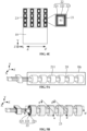
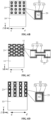
- FIG. 2A to FIG. 2S , FIG. 3A to FIG. 3E , FIG. 4A to FIG. 4E and FIG. 5A to FIG. 5E are schematic structural diagrams during forming a semiconductor structure provided by the embodiments of the present disclosure.
- the cross-sectional views in the directions of a-a', b-b', c-c', and d-d' are only to clearly describe the internal structure of the semiconductor, and are not drawn to scale.
- the formation process of the semiconductor structure provided by the embodiments of the disclosure is described in detail below with reference to FIG. 2A to FIG. 2S , FIG. 3A to FIG. 3E , FIG. 4A to FIG. 4E , and FIG. 5A to FIG. 5E .
- FIG. 2A to FIG. 2F S101 is performed.
- a semiconductor substrate 10 is provided, in which stack structures 11 and isolation structures 14 alternately arranged along a first direction are provided on the semiconductor substrate 10.
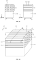
- FIG. 2A , FIG. 2C and FIG. 2E are three-dimensional views, and FIG. 2B , FIG. 2D and FIG. 2F are the sectional views of FIG. 2A , FIG. 2C and FIG. 2E , respectively.
- the isolation structures 14 may be formed by the following operations.
- An initial stack structure 11a is formed on the semiconductor substrate 10, in which the initial stack structure 11a includes first semiconductor layers 111 and second semiconductor layers 112 alternately stacked.
- the initial stack structure 11a is patterned to form the stack structures 11 and isolation trenches 13.
- An isolation material is filled in the isolation trenches 13 to form the isolation structures 14.
- the initial stack structure 11a is formed on the semiconductor substrate 10.
- the initial stack structure 11a includes the first semiconductor layers 111 and the second semiconductor layers 112 stacked alternately in sequence from bottom to up in the Y-axis direction.
- the first semiconductor layers 111 and the second semiconductor layers 112 may be formed by an epitaxial process.
- a semiconductor super lattice can be formed by alternately stacking the first semiconductor layers 111 and the second semiconductor layers 112.
- the thickness of each of the semiconductor layers ranges from layers of a few atoms to dozens of atoms, and the main semiconductor property of each of the semiconductor layers, such as the band gap and the doping level, can be controlled independently.
- the number of the first semiconductor layers 111 and the second semiconductor layers 112 in the stack structures 11 can be disposed according to the required capacitance density (or the storage density).
- the number of the first semiconductor layers 111 and the second semiconductor layers 112 may be 2 to 2000.
- the stack structures 11 and the isolation trenches 13 may be formed by the following operations.
- a first mask layer 12 with a first preset pattern is formed on a surface of the initial stack structure 11a.
- the first preset pattern includes a plurality of first preset sub-patterns H arranged along X-axis direction in sequence, and first preset sub-patterns H expose part of the initial stack structure 11a.
- the initial stack structure 11a is etched with the first mask layer 12 to remove the initial stack structure 11a exposed by the first mask layer 12 and form the stack structures 11 and the isolation trenches 13.
- the initial stack structure 11a can be etched by a high aspect ratio (HAR) technology to form the stack structures 11 and the isolation trenches 13.
- HAR high aspect ratio
- a dry etching process or a wet etching process may be adopted to remove the first mask layer 12 and expose the top surfaces of the stack structures 11.
- the isolation material is filled in the isolation trenches 13 to form the isolation structures 14.
- the isolation material may be silicon oxide, silicon nitride or silicon oxynitride.
- the isolation material located the surfaces of the stack structures 11 is not shown in FIG. 2E to FIG. 2J.
- FIG. 2G to FIG. 2J S102 is performed.
- a support structure is formed in the stack structures and the isolation structures.
- FIG. 2G and FIG. 2I are three-dimensional views, and FIG. 2H and FIG. 2J are the sectional views of the FIG. 2G and FIG. 2I , respectively.
- the support structure 15 may be formed by the following operations.
- a second mask layer (not shown) with a second preset pattern is formed on the surfaces of the stack structures 11 and the isolation structures 14.
- the second preset pattern exposes part of each of the stack structures 11 and part of each of the isolation structures 14.
- the exposed isolation structures 14 and the first semiconductor layers 111 of the exposed stack structures 11 are etched to be removed by the second mask layer to form etching grooves 16 as shown in FIG. 2G and FIG. 2H .
- a support material is filled in the etching grooves 16 to form the support structure 15 as shown in FIG. 2I and FIG. 2J.
- the support material may be silicon nitride or silicon carbonitride.
- the method for forming a semiconductor structure further includes: removing the second mask layer having the second preset pattern.
- the second mask layer may be removed by a dry etching technology or a wet etching technology to expose the top surfaces of the isolation structures 14.
- the support structure 15 can also be used to support the capacitor structures, thereby improving the stack stability of capacitor structures.
- FIG. 2K to FIG. 2O S103 is performed.
- the stack structures 11 and the isolation structures 14 are etched to form a plurality of zigzag first semiconductor pillars 17 in an array arrangement along the first direction and a second direction, and interspaces are formed between the zigzag first semiconductor pillars.
- Each of the zigzag first semiconductor pillars 17 includes first convex structures 21 and first concave structures 20 alternately arranged along a third direction, and the zigzag first semiconductor pillars 17 are supported by the support structure 15.
- FIG. 2K and FIG. 2L are three-dimensional views
- FIG. 2M is a sectional view of FIG. 2L
- FIG. 2N and FIG. 2O are sectional views.
- the zigzag first semiconductor pillars 17 may be formed by the following operations.
- a mask layer 19 with a specific pattern D is formed on the surfaces of the stack structures 11 and the isolation structures 14.
- the specific pattern D includes a plurality of sub-patterns E arranged along Z-axis direction in sequence, and the sub-patterns E exposes part of each of the stack structures 11 and part of each of the isolation structures 14.
- isolation structures 14 exposed by the sub-patterns E and first semiconductor layers 111 of the stack structures exposed by the sub-patterns E are removed by a dry etching technology or a wet etching technology.
- the first semiconductor layers 111 since the first semiconductor layers 111 have a higher etching selection ratio relative to the second semiconductor layers 112, the first semiconductor layers 111 can be removed without damaging the second semiconductor layers 112.
- the second semiconductor layers 112 in the stack structures 11 exposed by the sub-patterns E are thinned to form first concave structures 20.
- Untreated parts of the second semiconductor layers 112 constitute the first convex structures 21, and a projection area of each of the first convex structures 21 on the Z-axis direction is greater than a projection area of each of the first concave structures 20 on the Z-axis direction.
- the method for forming a semiconductor structure further includes: removing the mask layer 19, the remaining first semiconductor layers 111 and the remaining isolation structures 14 to expose the first convex structures 21.
- the method for forming a semiconductor structure further includes: performing ion implantation on the zigzag first semiconductor pillars 17.
- metal ions e.g. sodium ions
- the zigzag first semiconductor pillar 17 would act as a part of the lower electrode of the capacitor structure, the contact resistance between the lower electrode and the drain can be reduced by performing ion implantation on the zigzag first semiconductor pillar 17, thereby reducing the power consumption of the semiconductor structure.
- the method for forming a semiconductor structure further includes: forming a metal silicide on the surfaces of the zigzag first semiconductor pillars 17.
- a layer of metal material which may be, for example, any one of cobalt (Co), titanium (Ti), tantalum (Ta), nickel (Ni), tungsten (W), platinum (Pt), or palladium (Pd), may be deposited on the zigzag first semiconductor pillars 17.
- the metal material reacts with the zigzag first semiconductor pillars 17 by a rapid thermal annealing treatment, thereby forming the metal silicide on the surfaces of the zigzag first semiconductor pillars 17. Because the metal silicide has a low resistance value, the contact resistance between the lower electrode and the drain can be reduced, thereby reducing the power consumption of the semiconductor structure.
- FIG. 2P is a three-dimensional view
- FIG. 2Q, FIG. 2R and FIG. 2S are sectional views along a-a', b-b' and d-d' in FIG. 2P , respectively.
- the three-dimensional view of only one zigzag first semiconductor pillar 17 is shown in FIG. 2P .
- the semiconductor structure includes a plurality of zigzag first semiconductor pillars in an array arrangement along X-axis and Y-axis directions.
- the capacitor structures 22 may be formed by the following operations.
- a first electrode layer material, a dielectric layer material and a second electrode layer material are deposited in the interspace between the zigzag first electrode layers 17 in sequence to form a first electrode layer 221, a dielectric layer 222, and a second electrode layer 223, to form each of the capacitor structures 22.
- the first electrode material, the dielectric material, and the second electrode material may be deposited by any one of a selective atomic layer deposition process, a chemical vapor deposition process, a physical vapor deposition process or a spin coating process.
- the first electrode material and the second electrode material may include a metal or a metal nitride, for example, ruthenium (Ru) or titanium nitride.
- the dielectric material may include a high-K dielectric material, for example, one or any combination of lanthanum oxide (La 2 O 3 ), alumina (Al 2 O 3 ), hafnium oxide (HfO 2 ), hafnium oxynitride (HfON), hafnium silicate (HfSiOx) or zirconia (ZrO) 2 ).
- the first electrode material and the second electrode material may also be polysilicon.
- the method for forming a semiconductor structure further includes: filling a conducting material in an interspace between second electrode layers 223 to form a conducting layer 23.
- the conducting material may be polysilicon or any other suitable conducting materials, for example, germanium silicon or doped polysilicon.
- the first convex structures 21 and the first concave structures 20 together constitute the zigzag first semiconductor pillars 17, and the capacitor structures are formed subsequently in the interspace between the zigzag first semiconductor pillars 17. Since the projection area S1 of each of the first convex structures 21 on the third direction is greater than the projection area S2 of each of the first concave structures 20 on the third direction, the surface area of each of the zigzag first semiconductor pillars 17 in the embodiments of the disclosure is larger than the surface area of the cylindrical semiconductor pillar in the related art, and thus the effective area between the electrodes of each of the formed capacitor structures is larger and each of the formed capacitor structures has high capacitance. As a result, the sensing effect of the sense amplifier can be improved, and the retention time of data can be increased.
- the first convex structures 21 and the first concaves structure 20 are cuboids.
- a cross-section of the first concave structures 20 perpendicular to Z axis is a square with a side length of A
- a cross-section of the first convex structures 21 perpendicular to the Z axis is a square with a side length of B
- the first convex structures 21 and the first concave structures 20 in the Z-axis direction have a length of L.
- A, B and L conform to the equation: 4L ⁇ B + A, in which B > A.
- the range of A may be 10 to 30nm, and the range of B may be 30 to 50nm, and the range of L may be 5nm to 20nm.
- the method for forming a semiconductor structure before forming the capacitor structures, further includes: forming a gate-all-around structure and a bit line structure.
- the method for forming a semiconductor structure further includes: rounding the first concave structures 20 to form first cylinders 201.
- the first concave structures 20 can be etched with a tetramethylammonium hydroxide (TMAH) solution to form the first cylinders 201.
- TMAH tetramethylammonium hydroxide
- the method for forming a semiconductor structure further includes: etching the first convex structures 21 with the TMAH solution to round the first convex structures 21 to form second cylinders 211.
- the first cylinders 201 and the second cylinders 211 together constitute zigzag second semiconductor pillars 18a.
- the shielding layer before rounding the first convex structures 21, it is necessary to form a shielding layer on the surfaces of the first cylinders 201.
- the shielding layer has a different etching selection ratio with the zigzag second semiconductor pillars 18a and is used for protecting the first cylinders 201 from being damaged when the first convex structures 21 are rounded.
- the material of the shielding layer may be silicon dioxide, silicon nitride, silicon carbonitride, silicon hydroxide, or the like.
- the first convex structures 21 in the process of rounding the first concave structures 20, since the isolation structures 14 and the mask layer 19 are retained around the first convex structures 21, the first convex structures 21 can be protected from being damaged, so there is no need to form the shielding layer on the surfaces of the first convex structures 21.
- the method for forming a semiconductor structure further includes: performing ion implantation on the each zigzag second semiconductor pillars 18a, or forming the metal silicide on the surfaces of each zigzag second semiconductor pillars 18a.
- the metal ions e.g. sodium ions
- the metal ions may be used for performing ion implantation on the zigzag second semiconductor pillars 18a.
- the contact resistance between the lower electrode and the drain can be reduced by performing metal ion implantation on the zigzag second semiconductor pillar 18a, thereby reducing the power consumption of the semiconductor structure.
- the method for forming a semiconductor structure further includes: forming a first electrode layer 221, a dielectric layer 222 and a second electrode layer in sequence in the interspace between the zigzag second semiconductor pillars 18a to form each of capacitor structures 22 as shown in FIG. 3B to FIG. 3E .
- FIG. 3B is a three-dimensional view
- FIG. 3C, FIG. 3D and FIG. 3E are the sectional views along a-a', b-b' and d-d' in FIG. 3B , respectively.
- the semiconductor structure includes a plurality of zigzag second semiconductor pillars 18a in an array arrangement along X-axis and Y-axis directions.
- the method for forming a semiconductor structure further includes: filling a conducting material in the interspace between second electrode layers 223 to form a conducting layer 23.
- the first cylinders 201 and the second cylinders 211 together constitute each of the zigzag second semiconductor pillars 18a, and the capacitor structures are formed subsequently in the interspace between the zigzag second semiconductor pillars 18a. Since the projection area S4 of each second cylinder 211 on the third direction is greater than the projection area S3 of each first cylinder 201 on the third direction, the surface area of the zigzag second semiconductor pillar 18a in the embodiments of the disclosure is larger than the surface area of the cylindrical semiconductor pillar in the related art, and thus the effective area between the electrodes of each of the formed capacitor structures is larger and each of the formed capacitor structures has high capacitance. As a result, the sensing effect of the sense amplifier can be improved, and the retention time of data can be increased
- the first cylinders 201 and the second cylinders 211 are cylinders.
- a cross-section of the first cylinders 201 perpendicular to Z axis is a circle with a radius of r
- a cross-section of the second cylinders 211 perpendicular to Z axis is a circle with a radius of R
- the first cylinders 201 and the second cylinders 211 in the Z-axis direction have a length of L
- r, R, L conform to the equation: 2L ⁇ r + R, in which R is greater than r.
- the range of r may be 5 to 15 nm, and the range of R may be 15 to 30 nm, and the range of L may be 5nm to 20nm.
- the method for forming a semiconductor structure further includes: rounding the first concave structures 20 to form the first cylinders 201.
- the first concave structures 20 may be etched with the TMAH solution to form the first cylinders 201.
- the first cylinders 201 and the first convex structure 21 together constitute zigzag third semiconductor pillars 18b.
- the method for forming a semiconductor structure further includes: performing ion implantation on the zigzag third semiconductor pillars 18b, or forming the metal silicide on the surfaces of the zigzag third semiconductor pillars 18b.
- metal ions e.g. sodium ions
- the method for forming a semiconductor structure further includes: performing ion implantation on the zigzag third semiconductor pillars 18b, or forming the metal silicide on the surfaces of the zigzag third semiconductor pillars 18b.
- metal ions e.g. sodium ions
- the contact resistance between the lower electrode and the drain can be reduced by performing metal ion implantation on the zigzag third semiconductor pillar 18b, thereby reducing the power consumption of the semiconductor structure.
- the method for forming a semiconductor structure further includes: forming a first electrode layer 221, a dielectric layer 222 and a second electrode layer in sequence in the interspace between the zigzag third semiconductor pillars 18b to form each of capacitor structures 22 as shown in FIG. 4B to FIG. 4E .
- FIG. 4B is a three-dimensional view
- FIG. 4C, FIG. 4D and FIG. 4E are the sectional views along a-a', b-b' and d-d' in FIG. 4B , respectively.
- the semiconductor structure includes a plurality of zigzag third semiconductor pillars 18b in an array arrangement along X-axis and Y-axis directions.
- the method for forming a semiconductor structure further includes: filling a conducting material in the interspace between the second electrode layers 223 to form a conducting layer 23.
- the first cylinders 201 and the first convex structures 21 together constitute the zigzag third semiconductor pillars 18b, and the capacitor structures are formed subsequently in the interspace between the zigzag third semiconductor pillars 18b. Since the projection area S1 of the first convex structure 21 along the third direction is greater than the projection area S3 of the first cylinder 201 along the third direction, the surface area of each of the zigzag third semiconductor pillars 18b in the embodiments of the disclosure is larger than the surface area of the cylindrical semiconductor pillar in the related art, and thus the effective area between the electrodes of the each of formed capacitor structure is larger and each of the formed capacitor structures has high capacitance. As a result, the sensing effect of the sense amplifier can be improved, and the retention time of data can be increased.
- the method for forming a semiconductor structure further includes: etching the first convex structures 21 by the TMAH solution to round the first convex structures 21 to form second cylinders 211.
- the first concave structures 20 and the second cylinders 211 together constitute zigzag fourth semiconductor pillars 18c.
- the shielding layer before rounding the first convex structures 21, it is necessary to form a shielding layer on the surfaces of the first cylinders 201.
- the shielding layer has a different etching selection ratio with the zigzag fourth semiconductor pillars 18c and is used for protecting the first cylinders 201 from being damaged when the first convex structures 21 are rounded.
- the material of the shielding layer may be silicon dioxide, silicon nitride, silicon carbonitride, silicon hydroxide, or the like.
- the method for forming a semiconductor structure further includes: performing ion implantation on the zigzag fourth semiconductor pillars 18c, or forming the metal silicide on the surfaces of the zigzag fourth semiconductor pillars 18c.
- metal ions e.g. sodium ions
- the method for forming a semiconductor structure further includes: performing ion implantation on the zigzag fourth semiconductor pillars 18c, or forming the metal silicide on the surfaces of the zigzag fourth semiconductor pillars 18c.
- metal ions e.g. sodium ions
- the contact resistance between the lower electrode and the drain can be reduced by performing metal ion implantation on the zigzag fourth semiconductor pillar 18c, thereby reducing the power consumption of the semiconductor structure.
- the method for forming a semiconductor structure further includes: forming a first electrode layer 221, a dielectric layer 222 and a second electrode layer in sequence in the interspace between the zigzag fourth semiconductor pillars 18c to form each of the capacitor structures as shown in FIG. 5B to FIG. 5E .
- FIG. 5B is a three-dimensional view
- FIG. 5C, FIG. 5D and FIG. 5E are the sectional views along a-a', b-b' and d-d' in FIG. 5B , respectively.
- the semiconductor structure includes a plurality of zigzag fourth semiconductor pillar 18c in an array arrangement along X-axis and Y-axis directions.
- the method for forming a semiconductor structure further includes: filling a conducting material in the interspace between second electrode layers 223 to form a conducting layer 23.
- the first concave structures 20 and the second cylinders 211 together constitute the zigzag fourth semiconductor pillars 18c, and the capacitor structures are formed subsequently in the interspace between the zigzag fourth semiconductor pillars 18c. Since the projection area S4 of each of the second cylinders 211 along the third direction is greater than the projection area S2 of each of the first concave structures 20 along the third direction, the surface area of each of the zigzag fourth semiconductor pillars 18c in the embodiments of the disclosure is larger than the surface area of the cylindrical semiconductor pillar in the related art, and thus the effective area between the electrodes of each of the formed capacitor structures is larger and each of the formed capacitor structures has high capacitance. As a result, the sensing effect of the sense amplifier can be improved, and the retention time of data can be increased.
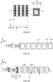
- embodiments of the disclosure also provide a semiconductor structure, and the semiconductor structure is formed by the method for forming a semiconductor structure in the above embodiments, and FIG. 6A to 6D are schematic structural diagrams of the semiconductor structure provided by the embodiments of the disclosure.
- FIG. 6A is a three-dimensional view of part of the semiconductor structure
- FIG. 6B to FIG. 6D are the sectional views along a-a', b-b', and d-d' in FIG. 6A .
- the semiconductor structure 100 includes a semiconductor substrate 10, and a support structure 15 and a plurality of zigzag first semiconductor pillars 17 located on a surface of the semiconductor substrate 10.
- the plurality of zigzag first semiconductor pillars 17 are in an array arrangement along a first direction (i.e., X-axis direction) and a second direction (i.e., Y-axis direction), and the plurality of zigzag first semiconductor pillars 17 are supported by the support structure 15.
- Each of the zigzag first semiconductor pillars 17 includes first convex structures 21 and first concave structures 20 arranged alternately along a third direction (i.e., Z-axis direction).
- a projection area S1 of each of the first convex structures 21 along the Z-axis direction is greater than a projection area S2 of each of the first concave structures 20 along the Z-axis direction.
- each of the first convex structures 21 may be a square pillar, a polygon pillar, or a circular pillar
- each of the first concave structures 20 may be a square pillar, a polygon pillar, or a circular pillar.
- the semiconductor structure 100 further include: capacitor structures 22 filled between the zigzag first semiconductor pillars 17.
- Each of the capacitor structures 22 includes a first electrode layer 221, a dielectric layer 222 and a second electrode layer 223.
- the semiconductor structure 100 further includes: a conducting layer 23 filled between second electrode layers 223.
- the semiconductor structure provided by the embodiments of the disclosure is similar to the method for forming a semiconductor structure in the above-mentioned embodiments.
- the semiconductor structure provided by the embodiments of the disclosure is similar to the method for forming a semiconductor structure in the above-mentioned embodiments.
- technical features not disclosed in detail in the embodiments of the disclosure please refer to the above-mentioned embodiment for understanding, and it will not be repeated here.
- the capacitor structures in the semiconductor structure are zigzag, the effective area between the electrodes of each of the capacitor structures is greater and each of the capacitor structures has high capacitance. In this way, the sensing effect of the sense amplifier can be improved, and the retention time of data can be increased.
- the disclosed devices and methods may be implemented in a non-target way.
- the above-described structure embodiments are only illustrative.
- the division of the units is only a logical function division, and there may be other division modes during actual implementation, such as, multiple units or components may be combined or integrated into another system, or some features may be ignored or not executed.
- the various parts shown or discussed are coupled, or directly coupled to each other.
- capacitor structures are formed in an interspace between zigzag first semiconductor pillars and each of the zigzag first semiconductor pillars has a greater surface area, an effective area between electrodes of each of the formed capacitor structures is greater and each of the formed capacitor structures has high capacitance. In this way, the sensing effect of the sense amplifier can be improved, and the retention time of data can be increased.
Landscapes
- Engineering & Computer Science (AREA)
- General Engineering & Computer Science (AREA)
- Physics & Mathematics (AREA)
- General Physics & Mathematics (AREA)
- Semiconductor Memories (AREA)
- Semiconductor Integrated Circuits (AREA)
Abstract
Description
- This application is based on and claims priority to
Chinese Patent Application No.202210729634.5, filed on June 24, 2022 - The disclosure relates to the technical field of semiconductors, and relates to, but is not limited to, a semiconductor structure and a method for forming the same.
- A sense amplifier (SA) is typically connected to a pair of complementary digital lines (for example, bit lines) for sensing the change of the signal on the two bit lines (BL) and amplifying the change of the signal. The signal sensed by the sense amplifier satisfies the following equation (1):

- In view of this, embodiments of the disclosure provide a semiconductor structure and a method for forming the same.
- In a first aspect, embodiments of the disclosure provide a method for forming a semiconductor structure, and the method includes the following operations.
- A semiconductor substrate is provided, in which stack structures and isolation structures alternately arranged along a first direction are formed on the semiconductor substrate.
- A support structure is formed in the stack structures and the isolation structures.
- The stack structures and the isolation structures are etched to form a plurality of zigzag first semiconductor pillars in an array arrangement along the first direction and a second direction, in which an interspace is formed between the zigzag first semiconductor pillars. Each of the zigzag first semiconductor pillars includes first convex structures and first concave structures alternately arranged along a third direction, and the zigzag first semiconductor pillars are supported by the support structure. The first direction, the second direction and the third direction are perpendicular to one another, and the second direction is perpendicular to a top surface of the semiconductor substrate.
- Capacitor structures are formed in the interspace.
- In a second aspect, embodiments of the disclosure provide an semiconductor structure, the semiconductor structure is formed by the method for forming a semiconductor structure described above, and the semiconductor structure includes: a semiconductor substrate; a plurality of zigzag first semiconductor pillars and a support structure located on a surface of the semiconductor substrate; and capacitor structures filled between the zigzag first semiconductor pillars.
- The plurality of the zigzag first semiconductor pillars are in an array arrangement along a first direction and a second direction and are supported by the support structure. Each of the zigzag first semiconductor pillars includes first convex structures and first concave structures alternately arranged along a third direction in sequence. The first direction, the second direction and the third direction are perpendicular to one another, and the second direction is perpendicular to a plane where the semiconductor substrate is located.
- According to the semiconductor structure and the method for forming a semiconductor structure provided by the embodiments of the disclosure, since the capacitor structures are formed in the interspace between the zigzag first semiconductor pillars and the zigzag first semiconductor pillars have greater surface areas, the effective area between the electrodes of each of the formed capacitor structures is greater, and each of the formed capacitor structures has high capacitance. In this way, the sensing effect of the sense amplifier can be improved, and the retention time of data can be increased.
- In the drawings (which are not necessarily drawn to scale), similar reference numerals may describe similar parts in different views. Similar reference numerals with different letter suffixes may represent different examples of similar parts. The various embodiments discussed herein are generally shown in the accompanying drawings by way of example and not limitation.
-
FIG. 1 is a schematic flowchart of a method for forming a semiconductor structure provided by embodiments of the disclosure. -
FIG. 2A to FIG. 2S ,FIG. 3A to FIG. 3E ,FIG. 4A to FIG. 4E andFIG. 5A to FIG. 5E are schematic structural diagrams during forming a semiconductor structure provided by embodiments of the present disclosure. -
FIG. 6A to FIG. 6D are schematic structural diagrams of a semiconductor structure provided by embodiments of the disclosure. - The reference numerals are as follows.
- 10, semiconductor substrate; 11, stack structure; 11a, initial stack structure; 111, first semiconductor layer; 112, second semiconductor layer; 12, first mask layer; 13, isolation trench; 14, isolation structure; 15, support structure; 16, etching groove; 17, zigzag first semiconductor pillar; 18a, zigzag second semiconductor pillar; 18b, zigzag third semiconductor pillar; 18c, zigzag fourth semiconductor pillar; 19, mask layer; 20, first concave structure; 21, first convex structure; 22, capacitor structure; 23, conducting layer; 201, first cylinder; 211, second cylinder; 221, first electrode layer; 222, dielectric layer; 223, second electrode layer; 100, semiconductor structure; H, first preset sub-pattern; D, specific pattern; and E, sub-pattern.
- Exemplary embodiments of the disclosure are described in more detail below with reference to the accompanying drawings. While exemplary embodiments of the present disclosure are shown in the drawings, it should be understood that the present disclosure may be implemented in various forms and should not be limited by the specific embodiments set forth herein. In contrast, these embodiments are provided to enable a more thorough understanding of the disclosure and to fully convey the scope of the disclosure to those skilled in the art.
- In the following description, numerous specific details are set forth in order to provide the more thorough understanding of the disclosure. However, it is apparent to those skilled in the art that the disclosure may be implemented without one or more of these details. In other embodiments, in order to avoid confusion with the present disclosure, some technical features known in the art are not described. That is, not all features of actual embodiments are described herein, and well-known functions and constructions are not described in detail.
- In the drawings, the dimensions of a layer, a region, an element or their relative dimensions may be magnified for clarity. The same reference numeral indicates the same element throughout.
- It should be understood that when the element or the layer is referred to as being "on ...", "adjacent to ...", "connected to ..." or "coupled to ..." other elements or layers, it may be directly on the other elements or layers, adjacent to, connected or coupled to the other elements or layers, or an intermediate element or layer may be present. In contrast, while the element is referred to as being "directly on ...", "directly adjacent to ...", "directly connected to ..." or "directly coupled to ..." other elements or layers, the intermediate element or layer is not present. It should be understood that although the terms first, second, third and the like may be used to describe various elements, components, regions, layers and/or sections, these elements, components, regions, layers and/or sections should not be limited by these terms. These terms are only used to distinguish one element, component, region, layer or section from another element, component, region, layer or section. Therefore, without departing from the teaching of the disclosure, a first element, component, region, layer or section discussed below may be represented as a second element, component, region, layer or section. While a second element, component, region, layer or section is discussed, it does not mean that a first element, component, region, layer or section is necessarily present in the disclosure.
- The terms used here are only intended to describe the specific embodiments and are not limitations to the disclosure. As used here, the singular forms "a", "an" and "said/the" are also intended to include plural forms, unless the context clearly indicates otherwise. It should also be understood that terms "composing" and/or "including", while used in the description, demonstrate the presence of the described features, integers, steps, operations, elements and/or components, but do not exclude the presence or addition of one or more other features, integers, steps, operations, elements, components, and/or groups. As used herein, the term "and/or" includes any and all combinations of related items listed.
- Before introducing the embodiments of the disclosure, three directions for that may be used to describe a stereo structure in the following embodiments are defined, and the three directions may include X-axis direction, Y-axis direction and Z-axis direction. In the directions of the top surface and the bottom surface of the substrate (i.e., the plane where the substrate is located), two directions that intersect each other (e.g., perpendicular to each other) are defined. For example, an extension direction of a capacitor structure can be defined as a third direction, and a direction in which stack structures and isolation structures are alternately arranged can be defined as a first direction, and the plane direction of the substrate can be determined based on the third direction and the first direction. The substrate may include a top surface on the front side and a bottom surface on the back side opposite the front side. When the flatness of the top surface and the bottom surface is ignored, the direction perpendicular to the top surface and the bottom surface of the substrate is defined as a second direction. It can be seen from this that the first direction, the second direction and the third direction are perpendicular to each other. In the embodiments of the disclosure, the first direction is defined as the X-axis direction, and the second direction is defined as the Y-axis direction, and the third direction is defined as the Z-axis direction.
- Embodiments of the disclosure provide a method for forming a semiconductor structure, and
FIG. 1 is a schematic flowchart of the method for forming a semiconductor structure provided by the embodiments of the disclosure. As shown inFIG. 1 , the method for forming a semiconductor structure includes the following operations. - At S101, a semiconductor substrate is provided, in which stack structures and isolation structures alternately arranged along a first direction are formed on the substrate.
- In the embodiments of the disclosure, the semiconductor substrate may be a silicon substrate, and the semiconductor substrate may also include other semiconductor elements, for example, germanium (Ge), or include semiconductor compounds, for example, silicon carbide (SiC), gallium arsenide (GaAs), gallium phosphide (GaP), indium phosphide (InP), indium arsenide (InAs), or indium antimonide (InSb), or include other semiconductor alloys, for example, silicon germanium (SiGe), gallium arsenic phosphide (GaAsP), aluminum indium arsenide (AlInAs), aluminum gallium arsenide (AlGaAs), gallium indium arsenide (GaInAs), gallium indium phosphide (GaInP), and/or gallium indium arsenide phosphide (GaInAsP) or combinations thereof.
- In the embodiments of the disclosure, the material of the isolation structures may be silicon oxide, silicon nitride, silicon oxynitride, or other suitable materials.
- In the embodiments of the disclosure, each of the stack structures includes first semiconductor layers and second semiconductor layers alternately stacked along the second direction. The material of the first semiconductor layers may be germanium, silicon germanium (SiGe), silicon carbide, silicon-on-insulator (SOI) or germanium-on-insulator (GOI). The second semiconductor layers may be silicon layers, and may also include other semiconductor elements, for example, germanium, or include semiconductor compounds for example, silicon carbide, gallium arsenide, gallium phosphide, indium phosphide, indium arsenide or indium antimonide, or include other semiconductor alloys, for example, silicon germanium, gallium arsenic phosphide, aluminum indium arsenide, aluminum gallium arsenide, gallium indium arsenide, gallium indium phosphide, and/or gallium indium arsenide phosphide or combinations thereof.
- In the embodiments of the disclosure, the materials of the first semiconductor layers and the second semiconductor layers should be different, because it needs to remove the first semiconductor layers in the stack structures subsequently and retain the second semiconductor layers. Therefore, the first semiconductor layers should have a greater selective etching ratio relative to the second semiconductor layers. For example, the etching selection ratio of the first semiconductor layers to the second semiconductor layers may be 5 to 15, so that the first semiconductor layers are prone to be removed by etching than the second semiconductor layers in the etching process.
- At S102, a support structure is formed in the stack structures and the isolation structures.
- In the embodiments of the disclosure, the material of the support structure may include at least one of silicon oxide, silicon nitride, silicon carbide nitride, silicon oxynitride or silicon boride nitride. The support structure can be formed by any suitable deposition process, for example, a chemical vapor deposition (CVD) process, a physical vapor deposition (PVD) process, an atomic layer deposition process (ALD) process, a spin coating process, a coating process or a thin-film process, etc.
- At S103, the stack structures and the isolation structures are etched to form a plurality of zigzag first semiconductor pillars in an array arrangement along the first direction and a second direction, and an interspace is formed between the zigzag first semiconductor pillars. Each of the zigzag first semiconductor pillars includes first convex structures and first concave structures alternately arranged along a third direction, and the zigzag first semiconductor pillars are supported by the support structure.
- In the embodiments of the disclosure, the stack structures and the isolation structures may be etched by a dry etching process (for example, a plasma etching process, a reactive ion etching process, or an ion milling process) to form the zigzag first semiconductor pillars. The gas used for the dry etching process may be one or any combination of trifluoromethane (CHF3), carbon tetrafluoride (CF4), difluoromethane (CH2F2), hydrobromic acid (HBr), chlorine (Cl2) or sulfur hexafluoride (SF6).
- In the embodiments of the disclosure, compared with a cylindrical first semiconductor pillar in the related art, the surface area of the each of the zigzag first semiconductor pillars composed of the first convex structures and the first concave structures alternately arranged is increased. In this way, when capacitor structures are formed in the interspace between the zigzag first semiconductor pillars, the effective area between the electrodes of each of the capacitor structures can be increased, thereby increasing the capacitance of the capacitor structures.
- At S104, the capacitor structures are formed in the interspace.
- In the embodiments of the disclosure, since the capacitor structures are formed in the interspace between the zigzag first semiconductor pillars and the zigzag first semiconductor pillars have greater surface areas, the effective area between the electrodes of each of the capacitor structures in the embodiments of the disclosure is greater, and thus each of the formed capacitor structures has high capacitance. In this way, the sensing effect of the sense amplifier can be improved, and the retention time of data can be increased.
-
FIG. 2A to FIG. 2S ,FIG. 3A to FIG. 3E ,FIG. 4A to FIG. 4E andFIG. 5A to FIG. 5E are schematic structural diagrams during forming a semiconductor structure provided by the embodiments of the present disclosure. The cross-sectional views in the directions of a-a', b-b', c-c', and d-d' are only to clearly describe the internal structure of the semiconductor, and are not drawn to scale. The formation process of the semiconductor structure provided by the embodiments of the disclosure is described in detail below with reference toFIG. 2A to FIG. 2S ,FIG. 3A to FIG. 3E ,FIG. 4A to FIG. 4E , andFIG. 5A to FIG. 5E . - First, referring to
FIG. 2A to FIG. 2F , S101 is performed. Asemiconductor substrate 10 is provided, in which stackstructures 11 andisolation structures 14 alternately arranged along a first direction are provided on thesemiconductor substrate 10.FIG. 2A ,FIG. 2C andFIG. 2E are three-dimensional views, andFIG. 2B ,FIG. 2D andFIG. 2F are the sectional views ofFIG. 2A ,FIG. 2C andFIG. 2E , respectively. - In some embodiments, the
isolation structures 14 may be formed by the following operations. Aninitial stack structure 11a is formed on thesemiconductor substrate 10, in which theinitial stack structure 11a includes first semiconductor layers 111 and second semiconductor layers 112 alternately stacked. Theinitial stack structure 11a is patterned to form thestack structures 11 andisolation trenches 13. An isolation material is filled in theisolation trenches 13 to form theisolation structures 14. - As shown in
FIG. 2A andFIG. 2B , theinitial stack structure 11a is formed on thesemiconductor substrate 10. Theinitial stack structure 11a includes the first semiconductor layers 111 and the second semiconductor layers 112 stacked alternately in sequence from bottom to up in the Y-axis direction. - In the embodiments of the disclosure, the first semiconductor layers 111 and the second semiconductor layers 112 may be formed by an epitaxial process. A semiconductor super lattice can be formed by alternately stacking the first semiconductor layers 111 and the second semiconductor layers 112. The thickness of each of the semiconductor layers ranges from layers of a few atoms to dozens of atoms, and the main semiconductor property of each of the semiconductor layers, such as the band gap and the doping level, can be controlled independently. The number of the first semiconductor layers 111 and the second semiconductor layers 112 in the
stack structures 11 can be disposed according to the required capacitance density (or the storage density). The more the number of the first semiconductor layers 111 and the second semiconductor layers 112, the higher the integration degree and the greater the capacitance density of the formed three-dimensional semiconductor structure. For example, the number of the first semiconductor layers 111 and the second semiconductor layers 112 may be 2 to 2000. - As shown in
FIG. 2C andFIG. 2D , thestack structures 11 and theisolation trenches 13 may be formed by the following operations. Afirst mask layer 12 with a first preset pattern is formed on a surface of theinitial stack structure 11a. The first preset pattern includes a plurality of first preset sub-patterns H arranged along X-axis direction in sequence, and first preset sub-patterns H expose part of theinitial stack structure 11a. Theinitial stack structure 11a is etched with thefirst mask layer 12 to remove theinitial stack structure 11a exposed by thefirst mask layer 12 and form thestack structures 11 and theisolation trenches 13. - In the embodiments of the disclosure, the
initial stack structure 11a can be etched by a high aspect ratio (HAR) technology to form thestack structures 11 and theisolation trenches 13. - In some embodiments, after forming the
stack structures 11 and theisolation trenches 13, a dry etching process or a wet etching process may be adopted to remove thefirst mask layer 12 and expose the top surfaces of thestack structures 11. - As shown in
FIG. 2E andFIG. 2F , the isolation material is filled in theisolation trenches 13 to form theisolation structures 14. The isolation material may be silicon oxide, silicon nitride or silicon oxynitride. - It should be noted that, in the process of filling the isolation material in the
isolation trenches 13 to form theisolation structures 14, part of the isolation material is often deposited on the surfaces ofstack structures 11, and then the surfaces of thestack structures 11 are treated by chemical mechanical polishing (CMP), so that a flat and smooth layer of the isolation material is located on the surfaces of each of thestack structures 11, and this layer of the isolation material is used for protecting the second semiconductor layers 112 located on the top surfaces of thestack structures 11 from being damaged when thestack structures 11 are processed subsequently. In the embodiments of the disclosure, for the convenience of describing the method for forming a semiconductor structure, the isolation material located the surfaces of thestack structures 11 is not shown inFIG. 2E to FIG. 2J. - Next, referring to
FIG. 2G to FIG. 2J, S102 is performed. A support structure is formed in the stack structures and the isolation structures.FIG. 2G andFIG. 2I are three-dimensional views, andFIG. 2H and FIG. 2J are the sectional views of theFIG. 2G andFIG. 2I , respectively. - In some embodiments, the
support structure 15 may be formed by the following operations. A second mask layer (not shown) with a second preset pattern is formed on the surfaces of thestack structures 11 and theisolation structures 14. The second preset pattern exposes part of each of thestack structures 11 and part of each of theisolation structures 14. The exposedisolation structures 14 and the first semiconductor layers 111 of the exposedstack structures 11 are etched to be removed by the second mask layer to formetching grooves 16 as shown inFIG. 2G andFIG. 2H . A support material is filled in theetching grooves 16 to form thesupport structure 15 as shown inFIG. 2I and FIG. 2J. In the embodiments of the disclosure, the support material may be silicon nitride or silicon carbonitride. - In some embodiments, after forming the
etching grooves 16, the method for forming a semiconductor structure further includes: removing the second mask layer having the second preset pattern. During implementation, the second mask layer may be removed by a dry etching technology or a wet etching technology to expose the top surfaces of theisolation structures 14. - In the embodiments of the disclosure, since capacitor structures would be formed in the interspace between the second semiconductor layers 112, the
support structure 15 can also be used to support the capacitor structures, thereby improving the stack stability of capacitor structures. - Next, referring to
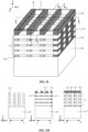
FIG. 2K to FIG. 2O , S103 is performed. Thestack structures 11 and theisolation structures 14 are etched to form a plurality of zigzagfirst semiconductor pillars 17 in an array arrangement along the first direction and a second direction, and interspaces are formed between the zigzag first semiconductor pillars. Each of the zigzagfirst semiconductor pillars 17 includes firstconvex structures 21 and firstconcave structures 20 alternately arranged along a third direction, and the zigzagfirst semiconductor pillars 17 are supported by thesupport structure 15.FIG. 2K andFIG. 2L are three-dimensional views,FIG. 2M is a sectional view ofFIG. 2L , andFIG. 2N and FIG. 2O are sectional views. - In some embodiments, the zigzag
first semiconductor pillars 17 may be formed by the following operations. - As shown in
FIG. 2K , amask layer 19 with a specific pattern D is formed on the surfaces of thestack structures 11 and theisolation structures 14. The specific pattern D includes a plurality of sub-patterns E arranged along Z-axis direction in sequence, and the sub-patterns E exposes part of each of thestack structures 11 and part of each of theisolation structures 14. - As shown in
FIG. 2L and FIG. 2M ,isolation structures 14 exposed by the sub-patterns E and first semiconductor layers 111 of the stack structures exposed by the sub-patterns E are removed by a dry etching technology or a wet etching technology. In the embodiments of the disclosure, since the first semiconductor layers 111 have a higher etching selection ratio relative to the second semiconductor layers 112, the first semiconductor layers 111 can be removed without damaging the second semiconductor layers 112. - As shown in
FIG. 2N , the second semiconductor layers 112 in thestack structures 11 exposed by the sub-patterns E are thinned to form firstconcave structures 20. Untreated parts of the second semiconductor layers 112 constitute the firstconvex structures 21, and a projection area of each of the firstconvex structures 21 on the Z-axis direction is greater than a projection area of each of the firstconcave structures 20 on the Z-axis direction. - As shown by
FIG. 2O , after forming the firstconcave structures 20, the method for forming a semiconductor structure further includes: removing themask layer 19, the remaining first semiconductor layers 111 and the remainingisolation structures 14 to expose the firstconvex structures 21. - In some embodiments, after forming the zigzag
first semiconductor pillars 17, the method for forming a semiconductor structure further includes: performing ion implantation on the zigzagfirst semiconductor pillars 17. For example, metal ions, e.g. sodium ions, may be used for performing ion implantation on the zigzagfirst semiconductor pillars 17. Since the zigzagfirst semiconductor pillar 17 would act as a part of the lower electrode of the capacitor structure, the contact resistance between the lower electrode and the drain can be reduced by performing ion implantation on the zigzagfirst semiconductor pillar 17, thereby reducing the power consumption of the semiconductor structure. - In some embodiments, after performing ion implantation on the zigzag
first semiconductor pillars 17, the method for forming a semiconductor structure further includes: forming a metal silicide on the surfaces of the zigzagfirst semiconductor pillars 17. During implementation, a layer of metal material, which may be, for example, any one of cobalt (Co), titanium (Ti), tantalum (Ta), nickel (Ni), tungsten (W), platinum (Pt), or palladium (Pd), may be deposited on the zigzagfirst semiconductor pillars 17. After that, the metal material reacts with the zigzagfirst semiconductor pillars 17 by a rapid thermal annealing treatment, thereby forming the metal silicide on the surfaces of the zigzagfirst semiconductor pillars 17. Because the metal silicide has a low resistance value, the contact resistance between the lower electrode and the drain can be reduced, thereby reducing the power consumption of the semiconductor structure. - Finally, referring to
FIG. 2P to FIG. 2S , S 104 is performed, andcapacitor structures 22 are formed in an interspace. -
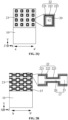
FIG. 2P is a three-dimensional view,FIG. 2Q, FIG. 2R andFIG. 2S are sectional views along a-a', b-b' and d-d' inFIG. 2P , respectively. It should be noted that the three-dimensional view of only one zigzagfirst semiconductor pillar 17 is shown inFIG. 2P . Actually, the semiconductor structure includes a plurality of zigzag first semiconductor pillars in an array arrangement along X-axis and Y-axis directions. - As shown in
FIG. 2P to FIG. 2S , in some embodiments, thecapacitor structures 22 may be formed by the following operations. A first electrode layer material, a dielectric layer material and a second electrode layer material are deposited in the interspace between the zigzag first electrode layers 17 in sequence to form afirst electrode layer 221, adielectric layer 222, and asecond electrode layer 223, to form each of thecapacitor structures 22. - In the embodiments of the disclosure, the first electrode material, the dielectric material, and the second electrode material may be deposited by any one of a selective atomic layer deposition process, a chemical vapor deposition process, a physical vapor deposition process or a spin coating process. The first electrode material and the second electrode material may include a metal or a metal nitride, for example, ruthenium (Ru) or titanium nitride. The dielectric material may include a high-K dielectric material, for example, one or any combination of lanthanum oxide (La2O3), alumina (Al2O3), hafnium oxide (HfO2), hafnium oxynitride (HfON), hafnium silicate (HfSiOx) or zirconia (ZrO)2). In other embodiments, the first electrode material and the second electrode material may also be polysilicon.
- In some embodiments, referring to
FIG. 2P to FIG. 2S , the method for forming a semiconductor structure further includes: filling a conducting material in an interspace between second electrode layers 223 to form aconducting layer 23. In the embodiments of the disclosure, the conducting material may be polysilicon or any other suitable conducting materials, for example, germanium silicon or doped polysilicon. - In the embodiments of the disclosure, the first
convex structures 21 and the firstconcave structures 20 together constitute the zigzagfirst semiconductor pillars 17, and the capacitor structures are formed subsequently in the interspace between the zigzagfirst semiconductor pillars 17. Since the projection area S1 of each of the firstconvex structures 21 on the third direction is greater than the projection area S2 of each of the firstconcave structures 20 on the third direction, the surface area of each of the zigzagfirst semiconductor pillars 17 in the embodiments of the disclosure is larger than the surface area of the cylindrical semiconductor pillar in the related art, and thus the effective area between the electrodes of each of the formed capacitor structures is larger and each of the formed capacitor structures has high capacitance. As a result, the sensing effect of the sense amplifier can be improved, and the retention time of data can be increased. - In some embodiments, the first
convex structures 21 and thefirst concaves structure 20 are cuboids. A cross-section of the firstconcave structures 20 perpendicular to Z axis is a square with a side length of A, a cross-section of the firstconvex structures 21 perpendicular to the Z axis is a square with a side length of B, and the firstconvex structures 21 and the firstconcave structures 20 in the Z-axis direction have a length of L. A, B and L conform to the equation: 4L < B + A, in which B > A. - In some embodiments, the range of A may be 10 to 30nm, and the range of B may be 30 to 50nm, and the range of L may be 5nm to 20nm.
- In some embodiments, before forming the capacitor structures, the method for forming a semiconductor structure further includes: forming a gate-all-around structure and a bit line structure.
- In some embodiments, as shown in
FIG. 3A , after forming the firstconcave structures 20, the method for forming a semiconductor structure further includes: rounding the firstconcave structures 20 to formfirst cylinders 201. For example, the firstconcave structures 20 can be etched with a tetramethylammonium hydroxide (TMAH) solution to form thefirst cylinders 201. - In some embodiments, after forming the first cylinders, the method for forming a semiconductor structure further includes: etching the first
convex structures 21 with the TMAH solution to round the firstconvex structures 21 to formsecond cylinders 211. Thefirst cylinders 201 and thesecond cylinders 211 together constitute zigzagsecond semiconductor pillars 18a. - In some embodiments, before rounding the first
convex structures 21, it is necessary to form a shielding layer on the surfaces of thefirst cylinders 201. The shielding layer has a different etching selection ratio with the zigzagsecond semiconductor pillars 18a and is used for protecting thefirst cylinders 201 from being damaged when the firstconvex structures 21 are rounded. For example, the material of the shielding layer may be silicon dioxide, silicon nitride, silicon carbonitride, silicon hydroxide, or the like. In the embodiments of the disclosure, in the process of rounding the firstconcave structures 20, since theisolation structures 14 and themask layer 19 are retained around the firstconvex structures 21, the firstconvex structures 21 can be protected from being damaged, so there is no need to form the shielding layer on the surfaces of the firstconvex structures 21. - In some embodiments, after forming the zigzag
second semiconductor pillars 18a, the method for forming a semiconductor structure further includes: performing ion implantation on the each zigzagsecond semiconductor pillars 18a, or forming the metal silicide on the surfaces of each zigzagsecond semiconductor pillars 18a. For example, the metal ions (e.g. sodium ions) may be used for performing ion implantation on the zigzagsecond semiconductor pillars 18a. - In the embodiments of the disclosure, since the zigzag
second semiconductor pillar 18a would act as a part of the lower electrode of the capacitor structure, the contact resistance between the lower electrode and the drain can be reduced by performing metal ion implantation on the zigzagsecond semiconductor pillar 18a, thereby reducing the power consumption of the semiconductor structure. - In some embodiments, after performing ion implantation on the zigzag
second semiconductor pillars 18a, or after forming the metal silicide on the surfaces of the zigzagsecond semiconductor pillars 18a, the method for forming a semiconductor structure further includes: forming afirst electrode layer 221, adielectric layer 222 and a second electrode layer in sequence in the interspace between the zigzagsecond semiconductor pillars 18a to form each ofcapacitor structures 22 as shown inFIG. 3B to FIG. 3E .FIG. 3B is a three-dimensional view, andFIG. 3C, FIG. 3D andFIG. 3E are the sectional views along a-a', b-b' and d-d' inFIG. 3B , respectively. It should be noted that the three-dimensional view of only one zigzagsecond semiconductor pillar 18a is shown inFIG. 3B . Actually, the semiconductor structure includes a plurality of zigzagsecond semiconductor pillars 18a in an array arrangement along X-axis and Y-axis directions. - In some embodiments, referring to
FIG. 3B to FIG. 3E , the method for forming a semiconductor structure further includes: filling a conducting material in the interspace between second electrode layers 223 to form aconducting layer 23. - In the embodiments of the disclosure, the
first cylinders 201 and thesecond cylinders 211 together constitute each of the zigzagsecond semiconductor pillars 18a, and the capacitor structures are formed subsequently in the interspace between the zigzagsecond semiconductor pillars 18a. Since the projection area S4 of eachsecond cylinder 211 on the third direction is greater than the projection area S3 of eachfirst cylinder 201 on the third direction, the surface area of the zigzagsecond semiconductor pillar 18a in the embodiments of the disclosure is larger than the surface area of the cylindrical semiconductor pillar in the related art, and thus the effective area between the electrodes of each of the formed capacitor structures is larger and each of the formed capacitor structures has high capacitance. As a result, the sensing effect of the sense amplifier can be improved, and the retention time of data can be increased - In some embodiments, the
first cylinders 201 and thesecond cylinders 211 are cylinders. A cross-section of thefirst cylinders 201 perpendicular to Z axis is a circle with a radius of r, a cross-section of thesecond cylinders 211 perpendicular to Z axis is a circle with a radius of R, thefirst cylinders 201 and thesecond cylinders 211 in the Z-axis direction have a length of L, and r, R, L conform to the equation: 2L< r + R, in which R is greater than r. - In some embodiments, the range of r may be 5 to 15 nm, and the range of R may be 15 to 30 nm, and the range of L may be 5nm to 20nm.
- In some embodiments, as shown in
FIG. 4A , after forming the firstconcave structures 20, the method for forming a semiconductor structure further includes: rounding the firstconcave structures 20 to form thefirst cylinders 201. For example, the firstconcave structures 20 may be etched with the TMAH solution to form thefirst cylinders 201. Thefirst cylinders 201 and the firstconvex structure 21 together constitute zigzagthird semiconductor pillars 18b. - In some embodiments, after forming the zigzag
third semiconductor pillars 18b, the method for forming a semiconductor structure further includes: performing ion implantation on the zigzagthird semiconductor pillars 18b, or forming the metal silicide on the surfaces of the zigzagthird semiconductor pillars 18b. For example, metal ions (e.g. sodium ions) may be used for performing ion implantation on the zigzagthird semiconductor pillars 18b. - In the embodiments of the disclosure, since the zigzag
third semiconductor pillar 18b would act as a part of the lower electrode of the capacitor structure, the contact resistance between the lower electrode and the drain can be reduced by performing metal ion implantation on the zigzagthird semiconductor pillar 18b, thereby reducing the power consumption of the semiconductor structure. - In some embodiments, after performing ion implantation on the zigzag
third semiconductor pillars 18b, or forming the metal silicide on the surfaces of the zigzagthird semiconductor pillars 18b, the method for forming a semiconductor structure further includes: forming afirst electrode layer 221, adielectric layer 222 and a second electrode layer in sequence in the interspace between the zigzagthird semiconductor pillars 18b to form each ofcapacitor structures 22 as shown inFIG. 4B to FIG. 4E .FIG. 4B is a three-dimensional view, andFIG. 4C, FIG. 4D andFIG. 4E are the sectional views along a-a', b-b' and d-d' inFIG. 4B , respectively. It should be noted that the three-dimensional view of only one zigzagthird semiconductor pillar 18b is shown inFIG. 4B . Actually, the semiconductor structure includes a plurality of zigzagthird semiconductor pillars 18b in an array arrangement along X-axis and Y-axis directions. - In some embodiments, referring to
FIG. 4B to FIG. 4E , the method for forming a semiconductor structure further includes: filling a conducting material in the interspace between the second electrode layers 223 to form aconducting layer 23. - In the embodiments of the disclosure, the
first cylinders 201 and the firstconvex structures 21 together constitute the zigzagthird semiconductor pillars 18b, and the capacitor structures are formed subsequently in the interspace between the zigzagthird semiconductor pillars 18b. Since the projection area S1 of the firstconvex structure 21 along the third direction is greater than the projection area S3 of thefirst cylinder 201 along the third direction, the surface area of each of the zigzagthird semiconductor pillars 18b in the embodiments of the disclosure is larger than the surface area of the cylindrical semiconductor pillar in the related art, and thus the effective area between the electrodes of the each of formed capacitor structure is larger and each of the formed capacitor structures has high capacitance. As a result, the sensing effect of the sense amplifier can be improved, and the retention time of data can be increased. - In some embodiments, as shown in
FIG. 5A , after forming the firstconcave structures 20 and the firstconvex structures 21, the method for forming a semiconductor structure further includes: etching the firstconvex structures 21 by the TMAH solution to round the firstconvex structures 21 to formsecond cylinders 211. The firstconcave structures 20 and thesecond cylinders 211 together constitute zigzagfourth semiconductor pillars 18c. - In some embodiments, before rounding the first
convex structures 21, it is necessary to form a shielding layer on the surfaces of thefirst cylinders 201. The shielding layer has a different etching selection ratio with the zigzagfourth semiconductor pillars 18c and is used for protecting thefirst cylinders 201 from being damaged when the firstconvex structures 21 are rounded. For example, the material of the shielding layer may be silicon dioxide, silicon nitride, silicon carbonitride, silicon hydroxide, or the like. - In some embodiments, after forming the zigzag
fourth semiconductor pillars 18c, the method for forming a semiconductor structure further includes: performing ion implantation on the zigzagfourth semiconductor pillars 18c, or forming the metal silicide on the surfaces of the zigzagfourth semiconductor pillars 18c. For example, metal ions (e.g. sodium ions) may be used for performing ion implantation on the zigzagfourth semiconductor pillars 18c. - In the embodiments of the disclosure, since the zigzag
fourth semiconductor pillar 18c would act as a part of the lower electrode of the capacitor structure, the contact resistance between the lower electrode and the drain can be reduced by performing metal ion implantation on the zigzagfourth semiconductor pillar 18c, thereby reducing the power consumption of the semiconductor structure. - In some embodiments, after performing ion implantation on the zigzag
fourth semiconductor pillars 18c, or after forming the metal silicide on the surfaces of the zigzagfourth semiconductor pillars 18c, the method for forming a semiconductor structure further includes: forming afirst electrode layer 221, adielectric layer 222 and a second electrode layer in sequence in the interspace between the zigzagfourth semiconductor pillars 18c to form each of the capacitor structures as shown inFIG. 5B to FIG. 5E .FIG. 5B is a three-dimensional view, andFIG. 5C, FIG. 5D andFIG. 5E are the sectional views along a-a', b-b' and d-d' inFIG. 5B , respectively. It should be noted that the three-dimensional view of only one zigzagfourth semiconductor pillar 18c is shown inFIG. 5B . Actually, the semiconductor structure includes a plurality of zigzagfourth semiconductor pillar 18c in an array arrangement along X-axis and Y-axis directions. - In some embodiments, referring to
FIG. 5B to FIG. 5E , the method for forming a semiconductor structure further includes: filling a conducting material in the interspace between second electrode layers 223 to form aconducting layer 23. - In the embodiments of the disclosure, the first
concave structures 20 and thesecond cylinders 211 together constitute the zigzagfourth semiconductor pillars 18c, and the capacitor structures are formed subsequently in the interspace between the zigzagfourth semiconductor pillars 18c. Since the projection area S4 of each of thesecond cylinders 211 along the third direction is greater than the projection area S2 of each of the firstconcave structures 20 along the third direction, the surface area of each of the zigzagfourth semiconductor pillars 18c in the embodiments of the disclosure is larger than the surface area of the cylindrical semiconductor pillar in the related art, and thus the effective area between the electrodes of each of the formed capacitor structures is larger and each of the formed capacitor structures has high capacitance. As a result, the sensing effect of the sense amplifier can be improved, and the retention time of data can be increased. - In addition, embodiments of the disclosure also provide a semiconductor structure, and the semiconductor structure is formed by the method for forming a semiconductor structure in the above embodiments, and
FIG. 6A to 6D are schematic structural diagrams of the semiconductor structure provided by the embodiments of the disclosure.FIG. 6A is a three-dimensional view of part of the semiconductor structure, andFIG. 6B to FIG. 6D are the sectional views along a-a', b-b', and d-d' inFIG. 6A . Thesemiconductor structure 100 includes asemiconductor substrate 10, and asupport structure 15 and a plurality of zigzagfirst semiconductor pillars 17 located on a surface of thesemiconductor substrate 10. - The plurality of zigzag
first semiconductor pillars 17 are in an array arrangement along a first direction (i.e., X-axis direction) and a second direction (i.e., Y-axis direction), and the plurality of zigzagfirst semiconductor pillars 17 are supported by thesupport structure 15. Each of the zigzagfirst semiconductor pillars 17 includes firstconvex structures 21 and firstconcave structures 20 arranged alternately along a third direction (i.e., Z-axis direction). - In the embodiments of the disclosure, a projection area S1 of each of the first
convex structures 21 along the Z-axis direction is greater than a projection area S2 of each of the firstconcave structures 20 along the Z-axis direction. - In some embodiments, each of the first
convex structures 21 may be a square pillar, a polygon pillar, or a circular pillar, and each of the firstconcave structures 20 may be a square pillar, a polygon pillar, or a circular pillar. - In some embodiments, referring to
FIG. 6A to FIG. 6D , thesemiconductor structure 100 further include:capacitor structures 22 filled between the zigzagfirst semiconductor pillars 17. Each of thecapacitor structures 22 includes afirst electrode layer 221, adielectric layer 222 and asecond electrode layer 223. - In some embodiments, the
semiconductor structure 100 further includes: a conductinglayer 23 filled between second electrode layers 223. - The semiconductor structure provided by the embodiments of the disclosure is similar to the method for forming a semiconductor structure in the above-mentioned embodiments. For technical features not disclosed in detail in the embodiments of the disclosure, please refer to the above-mentioned embodiment for understanding, and it will not be repeated here.
- In the embodiments of the disclosure, since the capacitor structures in the semiconductor structure are zigzag, the effective area between the electrodes of each of the capacitor structures is greater and each of the capacitor structures has high capacitance. In this way, the sensing effect of the sense amplifier can be improved, and the retention time of data can be increased.
- In several embodiments provided by the disclosure, it should be understood that the disclosed devices and methods may be implemented in a non-target way. The above-described structure embodiments are only illustrative. For example, the division of the units is only a logical function division, and there may be other division modes during actual implementation, such as, multiple units or components may be combined or integrated into another system, or some features may be ignored or not executed. In addition, the various parts shown or discussed are coupled, or directly coupled to each other.
- The features disclosed in several method or device embodiments provided by the disclosure may be arbitrarily combined without conflict to obtain a new method embodiment or device embodiment.
- The above are only some embodiments of the disclosure, and the protection scope of the disclosure is not limited to this. Changes or replacements can be easily thought of by any person skilled in the art and such changes or replacements should be covered by the protection scope of the disclosure. Therefore, the protection scope of the disclosure should be subject to the protection scope of the claims.
- According to a semiconductor structure and a method for forming a semiconductor structure provided by embodiments of the disclosure, since capacitor structures are formed in an interspace between zigzag first semiconductor pillars and each of the zigzag first semiconductor pillars has a greater surface area, an effective area between electrodes of each of the formed capacitor structures is greater and each of the formed capacitor structures has high capacitance. In this way, the sensing effect of the sense amplifier can be improved, and the retention time of data can be increased.
Claims (17)
- A method for forming a semiconductor structure, comprising:providing a semiconductor substrate, wherein stack structures and isolation structures alternately arranged along a first direction are formed on the semiconductor substrate;forming a support structure in the stack structures and the isolation structures;etching the stack structures and the isolation structures to form a plurality of zigzag first semiconductor pillars in an array arrangement along the first direction and a second direction, wherein an interspace is formed between the zigzag first semiconductor pillars; each of the zigzag first semiconductor pillars comprises first convex structures and first concave structures alternately arranged along a third direction, and the zigzag first semiconductor pillars are supported by the support structure; the first direction, the second direction and the third direction are perpendicular to one another, and the second direction is perpendicular to a top surface of the semiconductor substrate; andforming capacitor structures in the interspace.
- The method according to claim 1, wherein each of the stack structures comprises first semiconductor layers and second semiconductor layers alternately stacked along the second direction; and the zigzag first semiconductor pillars are formed by:forming a mask layer with a specific pattern on surfaces of the stack structures and the isolation structures, wherein the specific pattern comprises a plurality of sub-patterns arranged along the third direction in sequence, and the sub-patterns exposes part of each of the stack structures and part of each of the isolation structures; andforming the first concave structures by thinning each of the second semiconductor layers in each of the stack structures exposed by the sub-patterns; wherein an untreated part of each of the second semiconductor layers constitutes the first convex structures; and a projection area of each of the first convex structures along the third direction is greater than a projection area of each of the first concave structures along the third direction.
- The method according to claim 2, wherein before forming the first concave structures, the method further comprises:
removing the isolation structures exposed by the sub-patterns and the first semiconductor layers of the stack structures exposed by the sub-patterns by using the mask layer. - The method according to claim 3, wherein after forming the first concave structures, the method further comprises:
removing the mask layer, the remaining first semiconductor layers and the remaining isolation structures in sequence. - The method according to claim 2, wherein the stack structures and the isolation structures are formed by:forming an initial stack structure on the semiconductor substrate, wherein the initial stack structure comprises the first semiconductor layers and the second semiconductor layers alternately stacked;patterning the initial stack structure to form the stack structures and isolation trenches; andfilling an isolation material in the isolation trenches to form the isolation structures.
- The method according to claim 5, wherein patterning the initial stack structure to form the stack structures and the isolation trenches comprises:forming a first mask layer having a first preset pattern on a surface of the initial stack structure, wherein the first preset pattern comprises a plurality of first preset sub-patterns arranged along the first direction in sequence and the first preset pattern exposes part of the initial stack structure; andetching the initial stack structure by the first mask layer to remove the initial stack structure exposed by the first preset sub-patterns, to form the stack structures and the isolation trenches.
- The method according to any one of claims 2 to 6, wherein forming the support structure in the stack structures and the isolation structures comprises:forming a second mask layer having a second preset pattern on the surfaces of the stack structures and the isolation structures, wherein the second preset pattern exposes part of each of the stack structures and part of each of the isolation structures;removing the exposed isolation structures and the second semiconductor layers of the exposed stack structures by the second mask layer by etching to form etching grooves; andfilling a support material in the etching grooves to form the support structure.
- The method according to claim 1, wherein forming the capacitor structures in the interspace comprises:
forming a first electrode layer, a dielectric layer and a second electrode layer on a surface of each of the zigzag first semiconductor pillars to form the capacitor structures. - The method according to claim 8, wherein the method further comprises:
filling a conducting material in an interspace between the second electrode layers to form a conducting layer. - The method according to claim 7, wherein after forming the first concave structures and before removing the mask layer, the remaining first semiconductor layers and the remaining isolation structures in sequence, the method further comprises:
rounding the first concave structures to form first cylinders. - The method according to claim 10, wherein after removing the mask layer, the first semiconductor layers and the isolation structures in sequence, the method further comprises:
rounding the first convex structure to form second cylinders, wherein the first cylinders and the second cylinders together constitute the zigzag second semiconductor pillars. - The method according to claim 11, wherein the method further comprises:
forming the capacitor structures in the interspace between zigzag second semiconductor pillars to form the semiconductor structure. - The method according to claim 12, wherein the method further comprises:
performing ion implantation on the zigzag first semiconductor pillars or the zigzag second semiconductor pillars. - The method according to claim 13, wherein the method further comprises:
forming a metal silicide on surfaces of the zigzag first semiconductor pillars or the zigzag second semiconductor pillars. - A semiconductor structure comprising:a semiconductor substrate;a plurality of zigzag first semiconductor pillars and a support structure located on a surface of the semiconductor substrate; wherein the plurality of the zigzag first semiconductor pillars are in an array arrangement along a first direction and a second direction and are supported by the support structure; each of the zigzag first semiconductor pillar comprises first convex structures and first concave structures alternately arranged along a third direction in sequence; and the first direction, the second direction and the third direction are perpendicular to one another, and the second direction is perpendicular to a plane where the semiconductor substrate is located; andcapacitor structures filled between the zigzag first semiconductor pillars.
- The structure according to claim 15, wherein a projection area of each of the first convex structures on the third direction is greater than a projection area of each of the first concave structures on the third direction.
- The structure according to claim 15 or 16, wherein each of the capacitor structures comprises a first electrode layer, a dielectric layer and a second electrode layer; and the semiconductor structure further comprises a conducting layer; and
the conducting layer is filled between second electrode layers.
Applications Claiming Priority (2)
| Application Number | Priority Date | Filing Date | Title |
|---|---|---|---|
| CN202210729634.5A CN117334679A (en) | 2022-06-24 | 2022-06-24 | Semiconductor structures and methods of forming them |
| PCT/CN2022/105642 WO2023245772A1 (en) | 2022-06-24 | 2022-07-14 | Semiconductor structure and method for forming same |
Publications (3)
| Publication Number | Publication Date |
|---|---|
| EP4328969A1 true EP4328969A1 (en) | 2024-02-28 |
| EP4328969A4 EP4328969A4 (en) | 2024-07-24 |
| EP4328969B1 EP4328969B1 (en) | 2025-09-03 |
Family
ID=84891107
Family Applications (1)
| Application Number | Title | Priority Date | Filing Date |
|---|---|---|---|
| EP22836032.7A Active EP4328969B1 (en) | 2022-06-24 | 2022-07-14 | Semiconductor structure and method for forming same |
Country Status (4)
| Country | Link |
|---|---|
| US (1) | US12439615B2 (en) |
| EP (1) | EP4328969B1 (en) |
| JP (1) | JP2024526484A (en) |
| KR (1) | KR102864063B1 (en) |
Families Citing this family (2)
| Publication number | Priority date | Publication date | Assignee | Title |
|---|---|---|---|---|
| CN117580356A (en) * | 2022-08-04 | 2024-02-20 | 长鑫存储技术有限公司 | Semiconductor structures and methods of forming them |
| CN117580357A (en) | 2022-08-04 | 2024-02-20 | 长鑫存储技术有限公司 | Methods of forming semiconductor structures |
Family Cites Families (10)
| Publication number | Priority date | Publication date | Assignee | Title |
|---|---|---|---|---|
| JP3028774B2 (en) * | 1996-08-07 | 2000-04-04 | 日本電気株式会社 | Capacitor electrode formation method |
| JP2007184554A (en) | 2005-12-06 | 2007-07-19 | Canon Inc | Capacitor and circuit device using the same |
| CN101540325B (en) * | 2008-03-19 | 2011-07-13 | 财团法人工业技术研究院 | Electrode structure of storage capacitor and manufacturing method of storage capacitor structure |
| US10535659B2 (en) | 2017-09-29 | 2020-01-14 | Samsung Electronics Co., Ltd. | Semiconductor memory devices |
| KR102600110B1 (en) * | 2017-09-29 | 2023-11-10 | 삼성전자주식회사 | Semiconductor memory device |
| CN110504284B (en) * | 2018-05-17 | 2024-06-21 | 长鑫存储技术有限公司 | Columnar capacitor array structure and preparation method |
| KR102634622B1 (en) * | 2019-02-28 | 2024-02-08 | 에스케이하이닉스 주식회사 | Vertical memory device |
| KR102736487B1 (en) | 2019-06-27 | 2024-12-02 | 삼성전자주식회사 | Semiconductor memory device |
| US11903183B2 (en) | 2020-10-01 | 2024-02-13 | Micron Technology, Inc. | Conductive line contact regions having multiple multi-direction conductive lines and staircase conductive line contact structures for semiconductor devices |
| CN114582809B (en) | 2022-04-29 | 2022-07-29 | 长鑫存储技术有限公司 | Capacitor manufacturing method, capacitor and memory |
-
2022
- 2022-07-14 EP EP22836032.7A patent/EP4328969B1/en active Active
- 2022-07-14 KR KR1020237020408A patent/KR102864063B1/en active Active
- 2022-07-14 JP JP2023537377A patent/JP2024526484A/en active Pending
- 2022-09-29 US US17/936,846 patent/US12439615B2/en active Active
Also Published As
| Publication number | Publication date |
|---|---|
| EP4328969A4 (en) | 2024-07-24 |
| US20230014263A1 (en) | 2023-01-19 |
| KR20240001310A (en) | 2024-01-03 |
| KR102864063B1 (en) | 2025-09-23 |
| JP2024526484A (en) | 2024-07-19 |
| US12439615B2 (en) | 2025-10-07 |
| EP4328969B1 (en) | 2025-09-03 |
Similar Documents
| Publication | Publication Date | Title |
|---|---|---|
| KR102280471B1 (en) | Method of forming active patterns, active pattern array, and method of manufacturing semiconductor device | |
| EP4318586B1 (en) | Semiconductor structure and forming method therefor, and layout structure | |
| EP4328957B1 (en) | Semiconductor structure and forming method therefor, and layout structure | |
| EP4328969B1 (en) | Semiconductor structure and method for forming same | |
| JP7611398B2 (en) | Semiconductor structure, method for forming same, and layout structure | |
| EP4319529B1 (en) | Method for forming a semiconductor structure | |
| US12302556B2 (en) | Semiconductor device and method of fabricating the same | |
| US20230016558A1 (en) | Capacitor stack structure and method for forming same | |
| TW202401771A (en) | Semiconductor structure, method for forming same, and layout structure | |
| WO2024026940A1 (en) | Method for forming semiconductor structure | |
| WO2024036716A1 (en) | Semiconductor structure and forming method therefor | |
| WO2024026933A1 (en) | Semiconductor structure and formation method therefor | |
| TWI872554B (en) | Semiconductor structure and method for forming same | |
| TWI856686B (en) | Semiconductor structure, method for forming same and layout structure | |
| US20240057308A1 (en) | Semiconductor structure and method for forming same | |
| WO2023216392A1 (en) | Capacitor stack structure and forming method therefor | |
| WO2023236281A1 (en) | Semiconductor structure and method for forming same |
Legal Events
| Date | Code | Title | Description |
|---|---|---|---|
| STAA | Information on the status of an ep patent application or granted ep patent |
Free format text: STATUS: UNKNOWN |
|
| STAA | Information on the status of an ep patent application or granted ep patent |
Free format text: STATUS: THE INTERNATIONAL PUBLICATION HAS BEEN MADE |
|
| PUAI | Public reference made under article 153(3) epc to a published international application that has entered the european phase |
Free format text: ORIGINAL CODE: 0009012 |
|
| STAA | Information on the status of an ep patent application or granted ep patent |
Free format text: STATUS: REQUEST FOR EXAMINATION WAS MADE |
|
| 17P | Request for examination filed |
Effective date: 20230113 |
|
| AK | Designated contracting states |
Kind code of ref document: A1 Designated state(s): AL AT BE BG CH CY CZ DE DK EE ES FI FR GB GR HR HU IE IS IT LI LT LU LV MC MK MT NL NO PL PT RO RS SE SI SK SM TR |
|
| A4 | Supplementary search report drawn up and despatched |
Effective date: 20240620 |
|
| RIC1 | Information provided on ipc code assigned before grant |
Ipc: H01L 29/423 20060101ALI20240614BHEP Ipc: H01L 29/786 20060101ALI20240614BHEP Ipc: H01L 23/544 20060101ALI20240614BHEP Ipc: G01R 31/28 20060101ALI20240614BHEP Ipc: H01L 21/308 20060101ALI20240614BHEP Ipc: H10B 12/00 20230101ALI20240614BHEP Ipc: H01L 23/64 20060101AFI20240614BHEP |
|
| STAA | Information on the status of an ep patent application or granted ep patent |
Free format text: STATUS: EXAMINATION IS IN PROGRESS |
|
| 17Q | First examination report despatched |
Effective date: 20250228 |
|
| GRAP | Despatch of communication of intention to grant a patent |
Free format text: ORIGINAL CODE: EPIDOSNIGR1 |
|
| STAA | Information on the status of an ep patent application or granted ep patent |
Free format text: STATUS: GRANT OF PATENT IS INTENDED |
|
| RIC1 | Information provided on ipc code assigned before grant |
Ipc: H10D 30/67 20250101ALI20250521BHEP Ipc: H10D 1/68 20250101ALI20250521BHEP Ipc: H01L 23/544 20060101ALI20250521BHEP Ipc: G01R 31/28 20060101ALI20250521BHEP Ipc: H01L 21/308 20060101ALI20250521BHEP Ipc: H10B 12/00 20230101ALI20250521BHEP Ipc: H01L 23/64 20060101AFI20250521BHEP |
|
| GRAS | Grant fee paid |
Free format text: ORIGINAL CODE: EPIDOSNIGR3 |
|
| DAV | Request for validation of the european patent (deleted) | ||
| DAX | Request for extension of the european patent (deleted) | ||
| INTG | Intention to grant announced |
Effective date: 20250603 |
|
| GRAA | (expected) grant |
Free format text: ORIGINAL CODE: 0009210 |
|
| STAA | Information on the status of an ep patent application or granted ep patent |
Free format text: STATUS: THE PATENT HAS BEEN GRANTED |
|
| AK | Designated contracting states |
Kind code of ref document: B1 Designated state(s): AL AT BE BG CH CY CZ DE DK EE ES FI FR GB GR HR HU IE IS IT LI LT LU LV MC MK MT NL NO PL PT RO RS SE SI SK SM TR |
|
| P01 | Opt-out of the competence of the unified patent court (upc) registered |
Free format text: CASE NUMBER: UPC_APP_2502_4328969/2025 Effective date: 20250805 |
|
| REG | Reference to a national code |
Ref country code: CH Ref legal event code: EP |
|
| REG | Reference to a national code |
Ref country code: DE Ref legal event code: R096 Ref document number: 602022020938 Country of ref document: DE |
|
| REG | Reference to a national code |
Ref country code: IE Ref legal event code: FG4D |
|
| REG | Reference to a national code |
Ref country code: DE Ref legal event code: R079 Ref document number: 602022020938 Country of ref document: DE Free format text: PREVIOUS MAIN CLASS: H01L0023640000 Ipc: H10W0044000000 |
|
| REG | Reference to a national code |
Ref country code: NL Ref legal event code: MP Effective date: 20250903 |
|
| PG25 | Lapsed in a contracting state [announced via postgrant information from national office to epo] |
Ref country code: NO Free format text: LAPSE BECAUSE OF FAILURE TO SUBMIT A TRANSLATION OF THE DESCRIPTION OR TO PAY THE FEE WITHIN THE PRESCRIBED TIME-LIMIT Effective date: 20251203 |
|
| REG | Reference to a national code |
Ref country code: LT Ref legal event code: MG9D |
|
| PG25 | Lapsed in a contracting state [announced via postgrant information from national office to epo] |
Ref country code: FI Free format text: LAPSE BECAUSE OF FAILURE TO SUBMIT A TRANSLATION OF THE DESCRIPTION OR TO PAY THE FEE WITHIN THE PRESCRIBED TIME-LIMIT Effective date: 20250903 |
|
| PG25 | Lapsed in a contracting state [announced via postgrant information from national office to epo] |
Ref country code: HR Free format text: LAPSE BECAUSE OF FAILURE TO SUBMIT A TRANSLATION OF THE DESCRIPTION OR TO PAY THE FEE WITHIN THE PRESCRIBED TIME-LIMIT Effective date: 20250903 |
|
| PG25 | Lapsed in a contracting state [announced via postgrant information from national office to epo] |
Ref country code: GR Free format text: LAPSE BECAUSE OF FAILURE TO SUBMIT A TRANSLATION OF THE DESCRIPTION OR TO PAY THE FEE WITHIN THE PRESCRIBED TIME-LIMIT Effective date: 20251204 |
|
| PG25 | Lapsed in a contracting state [announced via postgrant information from national office to epo] |
Ref country code: SE Free format text: LAPSE BECAUSE OF FAILURE TO SUBMIT A TRANSLATION OF THE DESCRIPTION OR TO PAY THE FEE WITHIN THE PRESCRIBED TIME-LIMIT Effective date: 20250903 |
|
| PG25 | Lapsed in a contracting state [announced via postgrant information from national office to epo] |
Ref country code: LV Free format text: LAPSE BECAUSE OF FAILURE TO SUBMIT A TRANSLATION OF THE DESCRIPTION OR TO PAY THE FEE WITHIN THE PRESCRIBED TIME-LIMIT Effective date: 20250903 |
|
| PG25 | Lapsed in a contracting state [announced via postgrant information from national office to epo] |
Ref country code: BG Free format text: LAPSE BECAUSE OF FAILURE TO SUBMIT A TRANSLATION OF THE DESCRIPTION OR TO PAY THE FEE WITHIN THE PRESCRIBED TIME-LIMIT Effective date: 20250903 Ref country code: PL Free format text: LAPSE BECAUSE OF FAILURE TO SUBMIT A TRANSLATION OF THE DESCRIPTION OR TO PAY THE FEE WITHIN THE PRESCRIBED TIME-LIMIT Effective date: 20250903 |
|
| PG25 | Lapsed in a contracting state [announced via postgrant information from national office to epo] |
Ref country code: RS Free format text: LAPSE BECAUSE OF FAILURE TO SUBMIT A TRANSLATION OF THE DESCRIPTION OR TO PAY THE FEE WITHIN THE PRESCRIBED TIME-LIMIT Effective date: 20251203 |
|
| PG25 | Lapsed in a contracting state [announced via postgrant information from national office to epo] |
Ref country code: ES Free format text: LAPSE BECAUSE OF FAILURE TO SUBMIT A TRANSLATION OF THE DESCRIPTION OR TO PAY THE FEE WITHIN THE PRESCRIBED TIME-LIMIT Effective date: 20250903 |
|
| REG | Reference to a national code |
Ref country code: AT Ref legal event code: MK05 Ref document number: 1834242 Country of ref document: AT Kind code of ref document: T Effective date: 20250903 |
|
| PG25 | Lapsed in a contracting state [announced via postgrant information from national office to epo] |
Ref country code: NL Free format text: LAPSE BECAUSE OF FAILURE TO SUBMIT A TRANSLATION OF THE DESCRIPTION OR TO PAY THE FEE WITHIN THE PRESCRIBED TIME-LIMIT Effective date: 20250903 |
|
| PG25 | Lapsed in a contracting state [announced via postgrant information from national office to epo] |
Ref country code: SM Free format text: LAPSE BECAUSE OF FAILURE TO SUBMIT A TRANSLATION OF THE DESCRIPTION OR TO PAY THE FEE WITHIN THE PRESCRIBED TIME-LIMIT Effective date: 20250903 |
|
| PG25 | Lapsed in a contracting state [announced via postgrant information from national office to epo] |
Ref country code: AT Free format text: LAPSE BECAUSE OF FAILURE TO SUBMIT A TRANSLATION OF THE DESCRIPTION OR TO PAY THE FEE WITHIN THE PRESCRIBED TIME-LIMIT Effective date: 20250903 |
|
| PG25 | Lapsed in a contracting state [announced via postgrant information from national office to epo] |
Ref country code: IT Free format text: LAPSE BECAUSE OF FAILURE TO SUBMIT A TRANSLATION OF THE DESCRIPTION OR TO PAY THE FEE WITHIN THE PRESCRIBED TIME-LIMIT Effective date: 20250903 |
|
| PG25 | Lapsed in a contracting state [announced via postgrant information from national office to epo] |
Ref country code: IS Free format text: LAPSE BECAUSE OF FAILURE TO SUBMIT A TRANSLATION OF THE DESCRIPTION OR TO PAY THE FEE WITHIN THE PRESCRIBED TIME-LIMIT Effective date: 20260103 |
|
| PG25 | Lapsed in a contracting state [announced via postgrant information from national office to epo] |
Ref country code: CZ Free format text: LAPSE BECAUSE OF FAILURE TO SUBMIT A TRANSLATION OF THE DESCRIPTION OR TO PAY THE FEE WITHIN THE PRESCRIBED TIME-LIMIT Effective date: 20250903 Ref country code: PT Free format text: LAPSE BECAUSE OF FAILURE TO SUBMIT A TRANSLATION OF THE DESCRIPTION OR TO PAY THE FEE WITHIN THE PRESCRIBED TIME-LIMIT Effective date: 20260105 |
|
| PG25 | Lapsed in a contracting state [announced via postgrant information from national office to epo] |
Ref country code: SK Free format text: LAPSE BECAUSE OF FAILURE TO SUBMIT A TRANSLATION OF THE DESCRIPTION OR TO PAY THE FEE WITHIN THE PRESCRIBED TIME-LIMIT Effective date: 20250903 Ref country code: EE Free format text: LAPSE BECAUSE OF FAILURE TO SUBMIT A TRANSLATION OF THE DESCRIPTION OR TO PAY THE FEE WITHIN THE PRESCRIBED TIME-LIMIT Effective date: 20250903 |