EP4328665A2 - Electronic device - Google Patents
Electronic device Download PDFInfo
- Publication number
- EP4328665A2 EP4328665A2 EP23174343.6A EP23174343A EP4328665A2 EP 4328665 A2 EP4328665 A2 EP 4328665A2 EP 23174343 A EP23174343 A EP 23174343A EP 4328665 A2 EP4328665 A2 EP 4328665A2
- Authority
- EP
- European Patent Office
- Prior art keywords
- light blocking
- blocking layer
- substrate
- electronic device
- spacer
- Prior art date
- Legal status (The legal status is an assumption and is not a legal conclusion. Google has not performed a legal analysis and makes no representation as to the accuracy of the status listed.)
- Granted
Links
Images




Classifications
-
- G—PHYSICS
- G02—OPTICS
- G02F—OPTICAL DEVICES OR ARRANGEMENTS FOR THE CONTROL OF LIGHT BY MODIFICATION OF THE OPTICAL PROPERTIES OF THE MEDIA OF THE ELEMENTS INVOLVED THEREIN; NON-LINEAR OPTICS; FREQUENCY-CHANGING OF LIGHT; OPTICAL LOGIC ELEMENTS; OPTICAL ANALOGUE/DIGITAL CONVERTERS
- G02F1/00—Devices or arrangements for the control of the intensity, colour, phase, polarisation or direction of light arriving from an independent light source, e.g. switching, gating or modulating; Non-linear optics
- G02F1/01—Devices or arrangements for the control of the intensity, colour, phase, polarisation or direction of light arriving from an independent light source, e.g. switching, gating or modulating; Non-linear optics for the control of the intensity, phase, polarisation or colour
- G02F1/13—Devices or arrangements for the control of the intensity, colour, phase, polarisation or direction of light arriving from an independent light source, e.g. switching, gating or modulating; Non-linear optics for the control of the intensity, phase, polarisation or colour based on liquid crystals, e.g. single liquid crystal display cells
- G02F1/133—Constructional arrangements; Operation of liquid crystal cells; Circuit arrangements
- G02F1/136—Liquid crystal cells structurally associated with a semi-conducting layer or substrate, e.g. cells forming part of an integrated circuit
- G02F1/1362—Active matrix addressed cells
- G02F1/136209—Light shielding layers, e.g. black matrix, incorporated in the active matrix substrate, e.g. structurally associated with the switching element
-
- G—PHYSICS
- G02—OPTICS
- G02F—OPTICAL DEVICES OR ARRANGEMENTS FOR THE CONTROL OF LIGHT BY MODIFICATION OF THE OPTICAL PROPERTIES OF THE MEDIA OF THE ELEMENTS INVOLVED THEREIN; NON-LINEAR OPTICS; FREQUENCY-CHANGING OF LIGHT; OPTICAL LOGIC ELEMENTS; OPTICAL ANALOGUE/DIGITAL CONVERTERS
- G02F1/00—Devices or arrangements for the control of the intensity, colour, phase, polarisation or direction of light arriving from an independent light source, e.g. switching, gating or modulating; Non-linear optics
- G02F1/01—Devices or arrangements for the control of the intensity, colour, phase, polarisation or direction of light arriving from an independent light source, e.g. switching, gating or modulating; Non-linear optics for the control of the intensity, phase, polarisation or colour
- G02F1/13—Devices or arrangements for the control of the intensity, colour, phase, polarisation or direction of light arriving from an independent light source, e.g. switching, gating or modulating; Non-linear optics for the control of the intensity, phase, polarisation or colour based on liquid crystals, e.g. single liquid crystal display cells
- G02F1/133—Constructional arrangements; Operation of liquid crystal cells; Circuit arrangements
- G02F1/1333—Constructional arrangements; Manufacturing methods
- G02F1/1339—Gaskets; Spacers; Sealing of cells
-
- G—PHYSICS
- G02—OPTICS
- G02F—OPTICAL DEVICES OR ARRANGEMENTS FOR THE CONTROL OF LIGHT BY MODIFICATION OF THE OPTICAL PROPERTIES OF THE MEDIA OF THE ELEMENTS INVOLVED THEREIN; NON-LINEAR OPTICS; FREQUENCY-CHANGING OF LIGHT; OPTICAL LOGIC ELEMENTS; OPTICAL ANALOGUE/DIGITAL CONVERTERS
- G02F1/00—Devices or arrangements for the control of the intensity, colour, phase, polarisation or direction of light arriving from an independent light source, e.g. switching, gating or modulating; Non-linear optics
- G02F1/01—Devices or arrangements for the control of the intensity, colour, phase, polarisation or direction of light arriving from an independent light source, e.g. switching, gating or modulating; Non-linear optics for the control of the intensity, phase, polarisation or colour
- G02F1/13—Devices or arrangements for the control of the intensity, colour, phase, polarisation or direction of light arriving from an independent light source, e.g. switching, gating or modulating; Non-linear optics for the control of the intensity, phase, polarisation or colour based on liquid crystals, e.g. single liquid crystal display cells
- G02F1/133—Constructional arrangements; Operation of liquid crystal cells; Circuit arrangements
- G02F1/1333—Constructional arrangements; Manufacturing methods
- G02F1/1339—Gaskets; Spacers; Sealing of cells
- G02F1/13394—Gaskets; Spacers; Sealing of cells spacers regularly patterned on the cell subtrate, e.g. walls, pillars
-
- G—PHYSICS
- G02—OPTICS
- G02F—OPTICAL DEVICES OR ARRANGEMENTS FOR THE CONTROL OF LIGHT BY MODIFICATION OF THE OPTICAL PROPERTIES OF THE MEDIA OF THE ELEMENTS INVOLVED THEREIN; NON-LINEAR OPTICS; FREQUENCY-CHANGING OF LIGHT; OPTICAL LOGIC ELEMENTS; OPTICAL ANALOGUE/DIGITAL CONVERTERS
- G02F1/00—Devices or arrangements for the control of the intensity, colour, phase, polarisation or direction of light arriving from an independent light source, e.g. switching, gating or modulating; Non-linear optics
- G02F1/01—Devices or arrangements for the control of the intensity, colour, phase, polarisation or direction of light arriving from an independent light source, e.g. switching, gating or modulating; Non-linear optics for the control of the intensity, phase, polarisation or colour
- G02F1/13—Devices or arrangements for the control of the intensity, colour, phase, polarisation or direction of light arriving from an independent light source, e.g. switching, gating or modulating; Non-linear optics for the control of the intensity, phase, polarisation or colour based on liquid crystals, e.g. single liquid crystal display cells
- G02F1/133—Constructional arrangements; Operation of liquid crystal cells; Circuit arrangements
- G02F1/1333—Constructional arrangements; Manufacturing methods
- G02F1/1339—Gaskets; Spacers; Sealing of cells
- G02F1/13398—Spacer materials; Spacer properties
-
- G—PHYSICS
- G02—OPTICS
- G02F—OPTICAL DEVICES OR ARRANGEMENTS FOR THE CONTROL OF LIGHT BY MODIFICATION OF THE OPTICAL PROPERTIES OF THE MEDIA OF THE ELEMENTS INVOLVED THEREIN; NON-LINEAR OPTICS; FREQUENCY-CHANGING OF LIGHT; OPTICAL LOGIC ELEMENTS; OPTICAL ANALOGUE/DIGITAL CONVERTERS
- G02F1/00—Devices or arrangements for the control of the intensity, colour, phase, polarisation or direction of light arriving from an independent light source, e.g. switching, gating or modulating; Non-linear optics
- G02F1/01—Devices or arrangements for the control of the intensity, colour, phase, polarisation or direction of light arriving from an independent light source, e.g. switching, gating or modulating; Non-linear optics for the control of the intensity, phase, polarisation or colour
- G02F1/13—Devices or arrangements for the control of the intensity, colour, phase, polarisation or direction of light arriving from an independent light source, e.g. switching, gating or modulating; Non-linear optics for the control of the intensity, phase, polarisation or colour based on liquid crystals, e.g. single liquid crystal display cells
- G02F1/133—Constructional arrangements; Operation of liquid crystal cells; Circuit arrangements
- G02F1/136—Liquid crystal cells structurally associated with a semi-conducting layer or substrate, e.g. cells forming part of an integrated circuit
- G02F1/1362—Active matrix addressed cells
- G02F1/136286—Wiring, e.g. gate line, drain line
-
- H—ELECTRICITY
- H10—SEMICONDUCTOR DEVICES; ELECTRIC SOLID-STATE DEVICES NOT OTHERWISE PROVIDED FOR
- H10K—ORGANIC ELECTRIC SOLID-STATE DEVICES
- H10K59/00—Integrated devices, or assemblies of multiple devices, comprising at least one organic light-emitting element covered by group H10K50/00
- H10K59/10—OLED displays
- H10K59/12—Active-matrix OLED [AMOLED] displays
- H10K59/124—Insulating layers formed between TFT elements and OLED elements
-
- H—ELECTRICITY
- H10—SEMICONDUCTOR DEVICES; ELECTRIC SOLID-STATE DEVICES NOT OTHERWISE PROVIDED FOR
- H10K—ORGANIC ELECTRIC SOLID-STATE DEVICES
- H10K59/00—Integrated devices, or assemblies of multiple devices, comprising at least one organic light-emitting element covered by group H10K50/00
- H10K59/10—OLED displays
- H10K59/12—Active-matrix OLED [AMOLED] displays
- H10K59/126—Shielding, e.g. light-blocking means over the TFTs
-
- H—ELECTRICITY
- H10—SEMICONDUCTOR DEVICES; ELECTRIC SOLID-STATE DEVICES NOT OTHERWISE PROVIDED FOR
- H10K—ORGANIC ELECTRIC SOLID-STATE DEVICES
- H10K59/00—Integrated devices, or assemblies of multiple devices, comprising at least one organic light-emitting element covered by group H10K50/00
- H10K59/10—OLED displays
- H10K59/12—Active-matrix OLED [AMOLED] displays
- H10K59/131—Interconnections, e.g. wiring lines or terminals
-
- H—ELECTRICITY
- H10—SEMICONDUCTOR DEVICES; ELECTRIC SOLID-STATE DEVICES NOT OTHERWISE PROVIDED FOR
- H10K—ORGANIC ELECTRIC SOLID-STATE DEVICES
- H10K59/00—Integrated devices, or assemblies of multiple devices, comprising at least one organic light-emitting element covered by group H10K50/00
- H10K59/80—Constructional details
- H10K59/87—Passivation; Containers; Encapsulations
- H10K59/871—Self-supporting sealing arrangements
- H10K59/8723—Vertical spacers, e.g. arranged between the sealing arrangement and the OLED
-
- G—PHYSICS
- G02—OPTICS
- G02F—OPTICAL DEVICES OR ARRANGEMENTS FOR THE CONTROL OF LIGHT BY MODIFICATION OF THE OPTICAL PROPERTIES OF THE MEDIA OF THE ELEMENTS INVOLVED THEREIN; NON-LINEAR OPTICS; FREQUENCY-CHANGING OF LIGHT; OPTICAL LOGIC ELEMENTS; OPTICAL ANALOGUE/DIGITAL CONVERTERS
- G02F1/00—Devices or arrangements for the control of the intensity, colour, phase, polarisation or direction of light arriving from an independent light source, e.g. switching, gating or modulating; Non-linear optics
- G02F1/01—Devices or arrangements for the control of the intensity, colour, phase, polarisation or direction of light arriving from an independent light source, e.g. switching, gating or modulating; Non-linear optics for the control of the intensity, phase, polarisation or colour
- G02F1/13—Devices or arrangements for the control of the intensity, colour, phase, polarisation or direction of light arriving from an independent light source, e.g. switching, gating or modulating; Non-linear optics for the control of the intensity, phase, polarisation or colour based on liquid crystals, e.g. single liquid crystal display cells
- G02F1/133—Constructional arrangements; Operation of liquid crystal cells; Circuit arrangements
- G02F1/1333—Constructional arrangements; Manufacturing methods
- G02F1/133377—Cells with plural compartments or having plurality of liquid crystal microcells partitioned by walls, e.g. one microcell per pixel
-
- G—PHYSICS
- G02—OPTICS
- G02F—OPTICAL DEVICES OR ARRANGEMENTS FOR THE CONTROL OF LIGHT BY MODIFICATION OF THE OPTICAL PROPERTIES OF THE MEDIA OF THE ELEMENTS INVOLVED THEREIN; NON-LINEAR OPTICS; FREQUENCY-CHANGING OF LIGHT; OPTICAL LOGIC ELEMENTS; OPTICAL ANALOGUE/DIGITAL CONVERTERS
- G02F1/00—Devices or arrangements for the control of the intensity, colour, phase, polarisation or direction of light arriving from an independent light source, e.g. switching, gating or modulating; Non-linear optics
- G02F1/01—Devices or arrangements for the control of the intensity, colour, phase, polarisation or direction of light arriving from an independent light source, e.g. switching, gating or modulating; Non-linear optics for the control of the intensity, phase, polarisation or colour
- G02F1/13—Devices or arrangements for the control of the intensity, colour, phase, polarisation or direction of light arriving from an independent light source, e.g. switching, gating or modulating; Non-linear optics for the control of the intensity, phase, polarisation or colour based on liquid crystals, e.g. single liquid crystal display cells
- G02F1/133—Constructional arrangements; Operation of liquid crystal cells; Circuit arrangements
- G02F1/1333—Constructional arrangements; Manufacturing methods
- G02F1/1335—Structural association of cells with optical devices, e.g. polarisers or reflectors
- G02F1/133509—Filters, e.g. light shielding masks
- G02F1/133512—Light shielding layers, e.g. black matrix
-
- G—PHYSICS
- G02—OPTICS
- G02F—OPTICAL DEVICES OR ARRANGEMENTS FOR THE CONTROL OF LIGHT BY MODIFICATION OF THE OPTICAL PROPERTIES OF THE MEDIA OF THE ELEMENTS INVOLVED THEREIN; NON-LINEAR OPTICS; FREQUENCY-CHANGING OF LIGHT; OPTICAL LOGIC ELEMENTS; OPTICAL ANALOGUE/DIGITAL CONVERTERS
- G02F1/00—Devices or arrangements for the control of the intensity, colour, phase, polarisation or direction of light arriving from an independent light source, e.g. switching, gating or modulating; Non-linear optics
- G02F1/01—Devices or arrangements for the control of the intensity, colour, phase, polarisation or direction of light arriving from an independent light source, e.g. switching, gating or modulating; Non-linear optics for the control of the intensity, phase, polarisation or colour
- G02F1/13—Devices or arrangements for the control of the intensity, colour, phase, polarisation or direction of light arriving from an independent light source, e.g. switching, gating or modulating; Non-linear optics for the control of the intensity, phase, polarisation or colour based on liquid crystals, e.g. single liquid crystal display cells
- G02F1/133—Constructional arrangements; Operation of liquid crystal cells; Circuit arrangements
- G02F1/1333—Constructional arrangements; Manufacturing methods
- G02F1/1339—Gaskets; Spacers; Sealing of cells
- G02F1/13396—Spacers having different sizes
-
- G—PHYSICS
- G02—OPTICS
- G02F—OPTICAL DEVICES OR ARRANGEMENTS FOR THE CONTROL OF LIGHT BY MODIFICATION OF THE OPTICAL PROPERTIES OF THE MEDIA OF THE ELEMENTS INVOLVED THEREIN; NON-LINEAR OPTICS; FREQUENCY-CHANGING OF LIGHT; OPTICAL LOGIC ELEMENTS; OPTICAL ANALOGUE/DIGITAL CONVERTERS
- G02F1/00—Devices or arrangements for the control of the intensity, colour, phase, polarisation or direction of light arriving from an independent light source, e.g. switching, gating or modulating; Non-linear optics
- G02F1/01—Devices or arrangements for the control of the intensity, colour, phase, polarisation or direction of light arriving from an independent light source, e.g. switching, gating or modulating; Non-linear optics for the control of the intensity, phase, polarisation or colour
- G02F1/13—Devices or arrangements for the control of the intensity, colour, phase, polarisation or direction of light arriving from an independent light source, e.g. switching, gating or modulating; Non-linear optics for the control of the intensity, phase, polarisation or colour based on liquid crystals, e.g. single liquid crystal display cells
- G02F1/133—Constructional arrangements; Operation of liquid crystal cells; Circuit arrangements
- G02F1/136—Liquid crystal cells structurally associated with a semi-conducting layer or substrate, e.g. cells forming part of an integrated circuit
- G02F1/1362—Active matrix addressed cells
- G02F1/136227—Through-hole connection of the pixel electrode to the active element through an insulation layer
-
- G—PHYSICS
- G02—OPTICS
- G02F—OPTICAL DEVICES OR ARRANGEMENTS FOR THE CONTROL OF LIGHT BY MODIFICATION OF THE OPTICAL PROPERTIES OF THE MEDIA OF THE ELEMENTS INVOLVED THEREIN; NON-LINEAR OPTICS; FREQUENCY-CHANGING OF LIGHT; OPTICAL LOGIC ELEMENTS; OPTICAL ANALOGUE/DIGITAL CONVERTERS
- G02F1/00—Devices or arrangements for the control of the intensity, colour, phase, polarisation or direction of light arriving from an independent light source, e.g. switching, gating or modulating; Non-linear optics
- G02F1/01—Devices or arrangements for the control of the intensity, colour, phase, polarisation or direction of light arriving from an independent light source, e.g. switching, gating or modulating; Non-linear optics for the control of the intensity, phase, polarisation or colour
- G02F1/13—Devices or arrangements for the control of the intensity, colour, phase, polarisation or direction of light arriving from an independent light source, e.g. switching, gating or modulating; Non-linear optics for the control of the intensity, phase, polarisation or colour based on liquid crystals, e.g. single liquid crystal display cells
- G02F1/133—Constructional arrangements; Operation of liquid crystal cells; Circuit arrangements
- G02F1/136—Liquid crystal cells structurally associated with a semi-conducting layer or substrate, e.g. cells forming part of an integrated circuit
- G02F1/1362—Active matrix addressed cells
- G02F1/1368—Active matrix addressed cells in which the switching element is a three-electrode device
-
- G—PHYSICS
- G02—OPTICS
- G02F—OPTICAL DEVICES OR ARRANGEMENTS FOR THE CONTROL OF LIGHT BY MODIFICATION OF THE OPTICAL PROPERTIES OF THE MEDIA OF THE ELEMENTS INVOLVED THEREIN; NON-LINEAR OPTICS; FREQUENCY-CHANGING OF LIGHT; OPTICAL LOGIC ELEMENTS; OPTICAL ANALOGUE/DIGITAL CONVERTERS
- G02F2201/00—Constructional arrangements not provided for in groups G02F1/00 - G02F7/00
- G02F2201/40—Arrangements for improving the aperture ratio
Definitions
- the disclosure involves an electronic device.
- the disclosure provides an electronic device, including an electronic device that may have an enhanced opening rate.
- the electronic device includes a substrate, a semiconductor layer, a light blocking layer, and a spacer.
- the semiconductor layer is disposed on the substrate and has a channel area.
- the light blocking layer is disposed between the substrate and the channel area.
- the spacer is disposed on the semiconductor layer. The light blocking layer overlaps with the spacer and the channel area.
- the electronic device includes a substrate, a semiconductor element, a light blocking layer, and a spacer.
- the semiconductor element is disposed on the substrate.
- the spacer is disposed on the semiconductor layer.
- the light blocking layer is disposed between the semiconductor element and the spacer. The light blocking layer overlaps with the spacer.
- a corresponding component for example, a film layer or region
- it may be directly on the other component or there may be other components therebetween.
- a component when referred to as being “directly on another component,” there is no component therebetween.
- the two components when a component is referred to as being “on another component “, the two components have a top-down relationship in a top view, and the component may be above or below the other component, and the top-down relationship depends on an orientation of the device.
- the electrical connection or coupling described in this disclosure may refer to direct connection or indirect connection.
- direct connection the terminals of the components on the two circuits are directly connected or connected to each other with a conductor line segment.
- indirect connection there are switches, diodes, capacitors, inductors, resistors, other suitable components, or a combination of the above components between the terminals of the components on the two circuits, but not limited thereto.
- the thickness, length and width may be measured by optical microscope (OM), and the thickness or width may be obtained by measuring the cross-sectional image in the electron microscope, but not limited thereto.
- any two values or directions used for comparison may have certain errors. If a first value is equal to a second value, it implies that there may be an error of about 10% between the first value and the second value; if a first direction is perpendicular to a second direction, an angle between the first direction and the second direction may be between 80 degrees and 100 degrees; if the first direction is parallel to the second direction, the angle between the first direction and the second direction may be between 0 degrees and 10 degrees.
- the electronic device of the disclosure may include a display device, an antenna device, a light-emitting device, a sensing device, a touching device, or a splicing device, but the disclosure is not limited thereto.
- the electronic device may be a bendable or flexible electronic device, but not limited thereto.
- the display device may be a non-self-luminous display device or a self-luminous display device.
- the electronic device may include, for example, diodes, liquid crystal, light-emitting diodes (LEDs), quantum dots (QDs), fluorescence, phosphor or other suitable display medium, or a combination of the above materials.
- the antenna device may be a liquid crystal type antenna device or a non-liquid crystal type antenna device
- the sensing device may be a sensing device for sensing capacitance, light, thermal energy or ultrasonic waves, but not limited thereto.
- the light-emitting diodes may, for example, include organic light-emitting diodes (OLEDs), mini LEDs, micro LEDs, or quantum dot LED (QLED, QDLED), but not limited to.
- the splicing device may be, for example, a display splicing device or an antenna splicing device, but is not limited thereto. It should be noted that the electronic device may be any combination of the above, but not limited thereto.
- the appearance of the electronic device may be rectangular, circular, polygonal, a shape with curved edges, or other suitable shapes.
- the electronic device may have a drive system, a control system, a light source system,... and other peripheral systems to support a display device, an antenna device, a wearable device (e.g., augmented reality or virtual reality), a vehicle-mounted device (e.g., a car windshield glass) or splicing device.
- FIG. 1 is a top schematic view of an electronic device according to the first embodiment of the disclosure.
- FIG. 2 is a cross-sectional schematic view based on the profile line A-A' of FIG. 1 . It is worth noting that some elements are omitted in FIG. 1 .
- an electronic device 10a of this embodiment includes a substrate 100, a semiconductor layer 200, and a light blocking layer 300a.
- the substrate 100 is, for example, a flexible or inflexible substrate.
- the material of the substrate 100 may, for example, include glass, plastic or a combination thereof.
- the material of the substrate 100 may include quartz, sapphire, polymethyl methacrylate (PMMA), polycarbonate (PC), polyimide (PI), polyethylene terephthalate (PET), other suitable materials, or a combination of the above materials, and disclosure is not limited thereto.
- the semiconductor layer 200 is disposed on the substrate 100 and has a channel area CH.
- the electronic device 10a includes a semiconductor element TFT.
- the semiconductor element TFT may include, for example, a gate G, a source S, a drain D, and the aforementioned semiconductor layer 200, but the disclosure is not limited thereto.
- the gate G overlaps with the semiconductor layer 200 section in a normal direction N of the substrate 100, and the region where the semiconductor layer 200 overlaps with the gate G is regarded as the channel area CH.
- a gate insulating layer GI is provided between the gate G and the semiconductor layer 200.
- the source S and the drain D are, for example, separated from each other and electrically connected to the semiconductor layer 200.
- an insulating layer IL1 and the aforementioned gate insulating layer GI are disposed between the source S (or the drain D) and the semiconductor layer 200.
- the source S and the drain D are respectively electrically connected to the semiconductor layer 200 through a hole H1 and a hole H2 penetrating the insulating layer IL1 and the gate insulating layer GI, but the disclosure is not limited thereto.
- the material of the gate insulating layer GI and the insulating layer IL1 may include, for example, inorganic materials (e.g., silicon oxide, silicon nitride, silicon oxynitride, or a stacking layer of at least two of the above materials), organic materials (e.g., polyimide resin, epoxy resin, or acryl resin), or a combination of the above, but disclosure is not limited thereto.
- the gate insulating layer GI and/or the insulating layer IL1 are monolayer structures or multilayer structures.
- the semiconductor element TFT is, for example, a top gate type thin film transistor. However, although this embodiment takes the top gate type thin film transistor as an example, the disclosure is not limited thereto.
- the light blocking layer 300a is disposed on the substrate 100.
- the light blocking layer 300a may be disposed between the substrate 100 and the semiconductor layer 200.
- the light blocking layer 300a may be disposed between the substrate 100 and the channel area CH of the semiconductor layer 200, but the disclosure is not limited thereto.
- the light blocking layer 300a overlaps with at least a portion of the channel area CH of the semiconductor layer 200 in the normal direction N of the substrate 100 (e.g., a direction perpendicular to the upper surface of the substrate 100), thereby improving the channel area CH from being deteriorated due to the ambient light from the outside.
- the light blocking layer 300a overlaps with the channel area CH of the semiconductor layer 200 in the normal direction N of the substrate 100.
- the light blocking layer 300a may include a material with relatively low reflectivity and transmittance.
- the light blocking layer 300a may include photoresist, ink, resin, colorant, metal and oxide thereof, other organic material, other suitable material, or a combination of the above.
- the reflectivity of the light blocking layer 300a may be greater than or equal to 0% and less than 70%.
- the light blocking layer 300a may include molybdenum, but the disclosure is not limited thereto.
- the electronic device 10a further includes an opposite substrate 100'.
- the opposite substrate 100' is, for example, disposed correspondingly to the substrate 100, and the material included in the opposite substrate 100' may be the same or similar to the substrate 100, which will not be repeated herein.
- the opposite substrate 100' may be replaced by a package layer.
- the package layer may provide protection, packaging, and/or planarization functions for the light-emitting/display unit, and the package layer may include organic material, inorganic material, and any combinations or mixtures thereof, but not limited thereto.
- a light blocking pattern BM and a color filter CF may be disposed on the opposite substrate 100', but the disclosure is not limited thereto.
- the light blocking pattern BM and the color filter CF are respectively disposed on the opposite substrate 100' facing the surface of the substrate 100, but the disclosure is not limited thereto. In other embodiments, the light blocking pattern BM and the color filter CF are, for example, respectively disposed on the surface of the substrate 100 facing the opposite substrate 100', but the disclosure is not limited thereto.
- the material of the light blocking pattern BM is, for example, a black resin or a metal material with low reflectivity, so as to block the internal elements and wires of the electronic device 10a that are not intended to be seen by the user, thereby improving the display performance of the electronic device 10a.
- the color filter CF may include, for example, a red filter pattern, a green filter pattern, or a blue filter pattern, so that the electronic device 10a has a colored display image, but the disclosure is not limited thereto.
- the light blocking layer 300a may include, for example, materials with relatively low reflectivity and transmittance, in other embodiments, the configuration of the light blocking layer 300a may replace at least a portion of the light blocking pattern BM to enhance the opening rate.
- the electronic device 10a further includes a display medium layer ML.
- the display medium layer ML is, for example, disposed between the substrate 100 and the opposite substrate 100'.
- the material of the display medium layer ML includes, for example, liquid crystal, but the disclosure is not limited thereto.
- the display medium included in the display medium layer ML is arranged, for example, by driving the semiconductor element TFT and the pixel electrode PE described below.
- the electronic device 10a further includes a spacer (not shown in this embodiment).
- the spacer is, for example, disposed on the semiconductor layer 200.
- the spacer is disposed between the substrate 100 and the opposite substrate 100' to support the substrate 100 and/or the opposite substrate 100'.
- the material included in the spacer is not particularly limited, and may include, for example, organic materials and/or organic photosensitive materials, but the disclosure is not limited thereto.
- the spacer may be trapezoidal.
- the electronic device 10a further includes an insulating layer BF, a gate line GL, a data line DL, an insulating layer IL2, a pixel electrode PE, an insulating layer IL3, and a common electrode CE.
- other insulating layers may be provided between the substrate 100 and the light blocking layer 300a, but the disclosure is not limited thereto.
- the insulating layer BF is, for example, disposed on the substrate 100.
- the insulating layer BF is disposed between the substrate 100 and the semiconductor layer 200 and covers the light blocking layer 300a, but the disclosure is not limited thereto.
- the material of the insulating layer BF may include, for example, an inorganic material (e.g., silicon oxide, silicon nitride, silicon oxynitride, or a stacking layer of at least two of the above materials), but the disclosure is not limited thereto.
- the gate line GL and the data line DL are, for example, disposed on the substrate 100.
- the gate line GL is disposed on the gate insulating layer GI and extends along a first direction D1
- the data line DL is disposed on the insulating layer IL1 and extends along a second direction D2.
- the first direction D1 is different from the second direction D2 or the first direction D1 is perpendicular to the second direction D2, and the first direction D1 and the second direction D2 are also respectively perpendicular to the normal direction N.
- the gate G in the semiconductor element TFT may be, for example, electrically connected to a corresponding gate line GL to receive a corresponding gate signal
- the source S in the semiconductor element TFT may be, for example, electrically connected to a corresponding data line DL to receive a corresponding data signal.
- the material of the gate line GL and the data line DL may include, for example, molybdenum (Mo), Titanium (Ti), Tantalum (Ta), Niobium (Nb), Hafnium (Hf), Nickel (Ni), Chromium (Cr), Cobalt (Co), Zirconium (Zr), Tungsten (W), Aluminum (Al), copper (Cu), silver (Ag), other suitable metal, alloy or combination of the above materials, and the disclosure is not limited thereto.
- the gate line GL and the data line DL may, for example, include the same or different material, and the disclosure is not limited thereto.
- the gate line GL has a width W G (e.g., the maximum width in the second direction D2) in the second direction D2 (e.g., a direction perpendicular to the first direction Dl), and the data line DL has a width W D (e.g., the maximum width in the first direction D1) in the first direction D1.
- W G e.g., the maximum width in the second direction D2
- W D e.g., the maximum width in the first direction D1
- the insulating layer IL2 is, for example, disposed on the insulating layer IL1.
- the insulating layer IL2 covers the source S and a portion of the drain D. That is, the insulating layer IL2 has a hole H3 that exposes a portion of the drain D, but the disclosure is not limited thereto.
- the material of the insulating layer IL2 may include, for example, inorganic materials (e.g., silicon oxide, silicon nitride, silicon oxynitride, or a stacking layer of at least two of the above materials), organic materials (e.g., polyimide resin, epoxy resin, or acryl resin), or a combination of the above, but disclosure is not limited thereto.
- the material of the insulating layer IL2 is, for example, an organic material, but the disclosure is not limited thereto.
- the insulating layer IL2 has a thickness t and a side wall IL2_s at the hole H3 thereof.
- the side wall IL2_s of the insulating layer IL2 and a direction DS parallel to the surface of the substrate 100 have an included angle ⁇ .
- the direction DS herein is, for example, any extended direction on the surface of the substrate 100 facing or facing away from the opposite substrate 100'.
- the direction DS is, for example, perpendicular to the normal direction N of the substrate 100.
- the hole H3 of the insulating layer IL2 has a lower bottom surface H3_B.
- the lower bottom surface H3_B of the hole H3 has an edge H3_E
- the light blocking layer 300a has an edge 300E1 near the edge H3_E.
- the edge 300E1 of the light blocking layer 300a and the edge H3_E of the hole H3 have a distance Y in the direction DS.
- the light blocking layer 300a overlaps with the hole H3 of the insulating layer IL2 in the normal direction N of the substrate 100, but the disclosure is not limited thereto.
- the thickness t of the insulating layer IL2, the included angle ⁇ between the side wall IL2_s of the insulating layer IL2 and the direction DS, and the distance Y between the edge 300E1 of the light blocking layer 300a and the edge H3_E of the hole H3 satisfy the following relational expression 1: t ⁇ cot( ⁇ ) ⁇ Y ⁇ t ⁇ cot( ⁇ ) +10 ⁇ m.
- the depth of the hole H3 of the insulating layer IL2 is therefore deeper than the holes of the remaining layers.
- the inversion of the liquid crystal in the region forming the hole H3 of the insulating layer IL2 is seriously affected by the terrain, and may not be able to present the inversion as expected.
- the liquid crystal is unable to be controlled as expected, resulting in liquid crystal disclination, which may cause a problem that deteriorates the display image quality of the electronic device 10a.
- the light blocking layer 300a of this embodiment may be used to block the regions where the liquid crystal is not well arranged due to the formation of the hole H3 of the insulating layer IL2.
- the display quality of the electronic device 10a is thereby improved or enhanced.
- the electronic device 10a further includes a light blocking layer 310.
- the light blocking layer 310 and the light blocking layer 300a may, for example, belong to the same layer and be patterns separated from each other. As shown in FIG. 1 and FIG. 2 , the light blocking layer 310 also overlaps with at least a portion of the channel area CH of the semiconductor layer 200 in the normal direction N of the substrate 100 (e.g., a direction perpendicular to the upper surface of the substrate 100). In this way, the situation in which the channel area CH is affected and deteriorated by the ambient light (e.g., the light from the back-light source) is improved. It is worth noting that the difference between the light blocking layer 310 and the light blocking layer 300a is that the light blocking layer 300a overlaps with the hole H3 of the insulating layer IL2 in the normal direction N of the substrate 100.
- the thickness t of the insulating layer IL2 in response to the substrate 100 and the opposite substrate 100' being paired and generating an offset, the thickness t of the insulating layer IL2, the included angle ⁇ between the side wall IL2_s of the insulating layer IL2 and the direction DS, and the distance Y between the edge 300E1 of the light blocking layer 300a and the edge H3_E of the hole H3 may be made to satisfy the above relational expression 1.
- the color mixing phenomenon caused by the inability of the light blocking pattern BM to completely block the region with the hole H3 of the insulating layer IL2 may also be reduced.
- the light blocking layer 300a may replace at least a portion of light blocking pattern BM in this embodiment to block the regions where the liquid crystal is not well arranged due to the formation of the hole H3 of the insulating layer IL2, thereby improving the display performance of the electronic device 10a.
- the pixel electrode PE is disposed on the insulating layer IL2.
- the pixel electrode PE is electrically connected to the drain D through the hole H3 of the insulating layer IL2, but the disclosure is not limited thereto.
- the material of the pixel electrode PE may include, for example, metal oxide conductive materials (e.g., indium tin oxide, indium zinc oxide, aluminum tin oxide, aluminum zinc oxide, indium germanium zinc oxide), but the disclosure is not limited thereto.
- the insulating layer IL3 is, for example, disposed on the insulating layer IL2.
- the insulating layer IL3 covers the pixel electrode PE disposed on the insulating layer IL2, but the disclosure is not limited thereto.
- the material of the insulating layer IL3 may include, for example, inorganic materials (e.g., silicon oxide, silicon nitride, silicon oxynitride, or a stacking layer of at least two of the above materials), organic materials (e.g., polyimide resin, epoxy resin, or acryl resin), or a combination of the above, but disclosure is not limited thereto.
- the insulating layer IL3 is partially filled in the hole H3 of the insulating layer IL2, but the disclosure is not limited thereto.
- the common electrode CE is, for example, disposed on the insulating layer IL3.
- the material of the common electrode CE may include, for example, metal oxide conductive materials (e.g., indium tin oxide, indium zinc oxide, aluminum tin oxide, aluminum zinc oxide, indium germanium zinc oxide), but the disclosure is not limited thereto.
- the common electrode CE is also partially filled in the hole H3 of the insulating layer IL2, but the disclosure is not limited thereto.
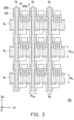
- FIG. 3 is a top schematic view of an electronic device according to the second embodiment of the disclosure. It is noted that the embodiment of FIG. 3 may use the reference numerals and a part of the contents of the embodiment of FIG. 1 , and the same or similar reference numerals are used to denote the same or similar elements, and the description of the same technical content is omitted.
- the difference between the electronic device 10b in FIG. 3 and the aforementioned electronic device 10a is that the light blocking layer 300b is disposed corresponding to the light blocking pattern BM on the opposite substrate 100', and the light blocking layer 300b may, for example, have a mesh structure.
- the light blocking layer 300b has a width W LS1 in the second direction D2, and the light blocking layer 300b has a width W LS2 in the first direction D1.
- the width W G of the gate line GL in the second direction D2 and the width W LS1 of the light blocking layer 300 in the second direction D2 satisfy the following relational expression 2: W G ⁇ W LS1 ⁇ 10 ⁇ W G .
- the width Wo of the data line DL in the first direction D1 and the width W LS2 of the light blocking layer 300 in the first direction D1 satisfy the following relational expression 3: W D ⁇ W LS2 ⁇ 10 ⁇ W D , but the disclosure is not limited thereto.
- the light blocking pattern BM included in the opposite substrate 100' is designed to at least block the light reflected by the gate line GL and/or the data line DL.
- the light blocking layer 300b in response to the width W G of the gate line GL and the width W LS1 of the light blocking layer 300b satisfying the relational expression 2 and/or the width W D of the data line DL and the width W LS2 of the light blocking layer 300b satisfying the relational expression 3, the light blocking layer 300b is disposed corresponding to the light blocking pattern BM (e.g., the light blocking layer 300b may overlap with at least a portion of the light blocking pattern BM along the normal direction N of the substrate 100).
- the light blocking layer 300b and the light blocking pattern BM may block the elements and wirings inside the electronic device 10b.
- the light blocking layer 300b of this embodiment may also have a pattern similar to the light blocking pattern BM, but the disclosure is not limited thereto.
- the light blocking layer 300b and the light blocking pattern BM may correspond to the gate line GL or the data line DL, or both the gate line GL and the data line DL.
- the light blocking layer 300b may have an area larger than the light blocking pattern BM in the normal direction N of the substrate 100.
- the material included in the light blocking layer 300b is, for example, a metal material with a reflectivity greater than or equal to 0% and less than 70%.
- the light blocking layer 300b may at least be used to block the light reflected by the gate line GL (e.g., the ambient light).
- the light blocking layer 300b may at least be used to block the light reflected by the data line DL (e.g., the ambient light).
- the light blocking layer 300b may be disposed on the same substrate (substrate 100) as the gate line GL and the data line DL (e.g., both are formed on the substrate 100), in response to the substrate 100 and the opposite substrate 100' being paired and generating an offset, the possibility of obtaining a poor color mixing phenomenon caused by the inability of the light blocking pattern BM to completely block the light reflected by the gate line GL and the data line DL may be reduced. The display performance of the electronic device 10b is thereby enhanced.
- the configuration area of the light blocking pattern BM may be relatively reduced.
- the electronic device 10b of this embodiment may reduce the configuration area of the light blocking pattern BM through the formation of the light blocking layer 300b, thereby reducing the drop of the opening rate caused by process variation.
- FIG. 4 is a top schematic view of an electronic device according to the third embodiment of the disclosure
- FIG. 5 is a cross-sectional schematic view based on the profile line B-B' of FIG. 4 .
- the embodiments of FIG. 4 and FIG. 5 may use the reference numerals and a part of the contents of the embodiments of FIG. 1 and 2 respectively, and the same or similar reference numerals are used to denote the same or similar elements, and the description of the same technical content is omitted.
- the difference between the electronic device 10c in FIG. 4 and the aforementioned electronic device 10a is that the light blocking layer 300c is disposed corresponding to the spacer 400. It should be noted that although the electronic device 10a in FIG. 1 omits the illustration of the spacer, the light blocking layer 300a of the electronic device 10a may also be disposed corresponding to the spacer.
- the spacer 400 is, for example, disposed on the semiconductor layer 200.
- the light blocking layer 300c overlaps with at least a portion of the spacer 400 and the channel area CH of the semiconductor layer 200 in the normal direction N of the substrate.
- the spacer 400 is disposed between the substrate 100 and the opposite substrate 100' to support the substrate 100 and/or the opposite substrate 100'.
- the material included in the spacer 400 is not particularly limited, and may include, for example, organic materials and/or organic photosensitive materials, but the disclosure is not limited thereto.
- the area of the upper bottom surface 400T of the spacer 400 is smaller than the area of the lower bottom surface 400B of the spacer 400. That is, the embodiment that the spacer 400 may be trapezoidal.
- the spacer 400 includes a side wall 400s1, and the side wall 400sl of the spacer 400 and the direction DS parallel to the surface of the substrate 100 have an included angle ⁇ .
- the spacer 400 has a thickness T in the normal direction N of the substrate 100.
- the thickness T of the spacer 400 is, for example, approximately the distance between the substrate 100 and the opposite substrate 100', but the disclosure is not limited thereto.
- the upper bottom surface 400T of the spacer 400 has an edge 400E1
- the light blocking layer 300c has an edge 300E2 near the edge 400E1 of the spacer 400.
- the edge 300E2 of the light blocking layer 300c and the edge 400E1 of the spacer 400 has a distance X in the direction DS.
- the light blocking layer 300c overlaps with the spacer 400 in the normal direction N of the substrate 100.
- the thickness T of the spacer 400, the included angle ⁇ between the side wall 400s1 of the spacer 400 and the direction DS, and the distance X between the edge 400E1 of the spacer 400 and the edge 300E2 of the light blocking layer 300c may satisfy the following relational expression 4: T ⁇ cot( ⁇ ) ⁇ X ⁇ T ⁇ cot( ⁇ ) +15 ⁇ m.
- the liquid crystal molecular is unable to be controlled as expected, resulting in liquid crystal disclination and causing the poor display quality of the electronic device 10c. Based on this, the above relational expression 4 is satisfied by making the thickness T of the spacer 400, the included angle ⁇ between the side wall 400s1 of the spacer 400 and the direction DS, and the distance X between the edge 400E1 of the spacer 400 and the edge 300E2 of the light blocking layer 300c.
- the light blocking layer 300c of this embodiment may block (1) a scratched region in contact with the spacer 400 and/or (2) the region with poor liquid crystal arrangement that overlaps with the spacer 400 in the normal direction N of the substrate 100 due to the configuration of the spacer 400, thereby maintain a good display quality.
- the above relational expression 4 is satisfied by making the thickness T of the spacer 400, the included angle ⁇ between the side wall 400s1 of the spacer 400 and the direction DS, and the distance X between the edge 400E1 of the spacer 400 and the edge 300E2 of the light blocking layer 300c.
- the possibility of obtaining a poor color mixing phenomenon caused by the inability of the light blocking pattern BM to completely block the region with the spacer 400 disposed may be reduced.
- the display performance of the electronic device 10c is thereby enhanced.
- the light blocking layer 300c in the electronic device 10c may also overlap with the hole H3 of the insulating layer IL2 in the normal direction N of the substrate 100, but the disclosure is not limited thereto.
- the electronic device 10c may also satisfy the above relational expression 1, so that the light blocking layer 300c of this embodiment is used to block the region with poor liquid crystal arrangement caused by the formation of the hole H3 of the insulating layer IL2, thereby maintaining the display quality of the electronic device 10c.
- the spacer 400 may overlap with at least a portion of the hole H3 and the light blocking layer 300c in the normal direction N, so as to improve the opening rate of the display apparatus.
- the spacer 400 may partially fill in the hole H3, but the disclosure is not limited thereto.
- FIG. 6 is a partial cross-sectional schematic view of an electronic device according to the fourth embodiment of the disclosure. It is noted that the embodiment of FIG. 6 may use the reference numerals and a part of the contents of the embodiment of FIG. 4 , and the same or similar reference numerals are used to denote the same or similar elements, and the description of the same technical content is omitted.
- the spacer 400 includes a main spacer 400M and a sub spacer 400S, and the area of the light blocking layer 300d disposed corresponding to the main spacer 400M may be larger than the area of the light blocking layer 300d disposed corresponding to the sub spacer 400S.
- the thickness of the main spacer 400M (e.g., the thickness T of the spacer 400 in the electronic device 10c) is, for example, greater than the thickness of the sub spacer 400S.
- the lower bottom surface of the main spacer 400M abuts against the element disposed on the substrate 100
- the upper bottom surface of the main spacer 400M abuts against the element disposed on the opposite substrate 100'.
- the lower bottom surface of the sub spacer 400S abuts against the element disposed on the substrate 100, and a distance is provided between the upper bottom surface of the sub spacer 400S and the element disposed on the opposite substrate 100', but the disclosure is not limited thereto.
- the sub spacer 400S may be, for example, formed on the opposite substrate 100'.
- the lower bottom surface of the sub spacer 400S e.g., the surface near the opposite substrate 100'
- the disclosure is not limited thereto.
- the area of the light blocking layer 300d disposed corresponding to the main spacer 400M is larger than the area of the light blocking layer 300d disposed corresponding to the sub spacer 400S.
- the width (e.g., the maximum width) 300W1 of the first section 300d1 of the light blocking layer 300d disposed corresponding to the main spacer 400M in the second direction D2 is greater than the width (e.g., the maximum width) 300W2 of the second section 300d2 of the light blocking layer 300d disposed corresponding to the sub spacer 400S in the second direction D2, which makes the area of the light blocking layer 300d (first section 300d1) disposed corresponding to the main spacer 400M larger than the area of the light blocking layer 300d (second section 300d2) disposed corresponding to the sub spacer 400S, but the disclosure is not limited thereto.
- the area of the light blocking layer 300d disposed corresponding to the main spacer 400M may be equal to the area of the light blocking layer 300d disposed corresponding to the sub spacer 400S, but the disclosure is not limited thereto.
- FIG. 7 is a partial cross-sectional schematic view of an electronic device according to the fifth embodiment of the disclosure. It is noted that the embodiment of FIG. 7 may use the reference numerals and a part of the contents of the embodiment of FIG. 5 , and the same or similar reference numerals are used to denote the same or similar elements, and the description of the same technical content is omitted.
- the light blocking layer includes a first light blocking layer 300e1 and a second light blocking layer 300e2,
- the first light blocking layer 300e1 is disposed between the substrate 100 and the channel area CH of the semiconductor layer 200
- the second light blocking layer 300e2 is disposed between the semiconductor element TFT and the spacer 400.
- the electronic device of the aforementioned embodiment does not show the second light blocking layer 300e2
- the second light blocking layer 300e2 may be mixed and matched with the aforementioned embodiment.
- the configuration relationship between the first light blocking layer 300e1 between the substrate 100 and the semiconductor layer 200 is similar to the aforementioned light blocking layer 300a, light blocking layer 300b, light blocking layer 300c, and light blocking layer 300d, the main difference is that the first light blocking layer 300e1 is not restricted to overlap with the hole H3, the light blocking pattern BM, and/or the spacer 400 in the normal direction N of substrate 100. However, the first light blocking layer 300e1 still overlaps with at least a portion of the channel area CH of the semiconductor layer 200 in the normal direction N of the substrate 100, thereby reducing the probability of the channel area CH being affected and deteriorated by the ambient light from the outside. In some embodiments, the first light blocking layer 300e1 overlaps with the channel area CH of the semiconductor layer 200 in the normal direction N of the substrate 100.
- the second light blocking layer 300e2 is disposed between the common electrode CE and the insulating layer IL3.
- the second light blocking layer 300e2 may be, for example, in contact with the common electrode CE, and partially filled in the hole H3 of the insulating layer IL2, but the disclosure is not limited thereto.
- the second light blocking layer 300e2 may overlap with at least a portion of the spacer 400. In this way, the (1) scratched region in contact with the spacer 400 and/or (2) the region with poor liquid crystal arrangement that substantially overlaps with the spacer 400 in the normal direction N of the substrate 100 due to the configuration of the spacer 400 is blocked, thereby maintaining the display quality of the electronic device 10e.
- the second light blocking layer 300e2 may also overlap with the hole H3 of the insulating layer IL2 in the normal direction N of the substrate 100, so that the second light blocking layer 300e2 may be used to block the region where the liquid crystal arrangement is poor due to the formation of the hole H3 of the insulating layer IL2.
- the light blocking layer may be, for example, a mesh structure, which is similar in shape to the light blocking layer 300d in FIG. 6 , but the disclosure is not limited thereto.
- the material of the first light blocking layer 300e1 and the second light blocking layer 300e2 is the same as or similar to that of the aforementioned light blocking layer 300a, which will not be repeated herein.
- the light blocking layer included in the electronic device of the embodiment of the disclosure has a novel design.
- the light blocking layer may overlap with at least a portion of the spacer in the normal direction of the substrate, or make the light blocking layer meet relational expression 4, so that the opening rate of the electronic device of the embodiment of the disclosure is enhanced.
- the process of forming the light blocking layer on the substrate is more stable than the process of forming the light blocking pattern on the opposite substrate.
- the electronic device of the embodiment of the disclosure may reduce the configuration area of the light blocking pattern by forming a light blocking layer on the substrate, thereby reducing the drop of the opening rate caused by process variation.
- the electronic device of the embodiment of the disclosure may reduce the probability of a drop of the opening rate caused by the offset between the substrate and the opposite substrate.
- the light blocking layer of the embodiment of the disclosure may block the insulating layer with a deeper opening (where the pixel electrode and the common electrode are disposed) in the normal direction of the substrate.
- the aforementioned light blocking layer may be made to satisfy the relational expression 1.
- the light blocking layer of the embodiment of the disclosure may overlap with at least a portion of the light blocking pattern in the normal direction of the substrate.
- the aforementioned light blocking layer may be made to satisfy the relational expression 2 and/or the relational expression 3.
Landscapes
- Physics & Mathematics (AREA)
- Nonlinear Science (AREA)
- Optics & Photonics (AREA)
- Crystallography & Structural Chemistry (AREA)
- Chemical & Material Sciences (AREA)
- General Physics & Mathematics (AREA)
- Mathematical Physics (AREA)
- Engineering & Computer Science (AREA)
- Microelectronics & Electronic Packaging (AREA)
- Devices For Indicating Variable Information By Combining Individual Elements (AREA)
- Solid State Image Pick-Up Elements (AREA)
- Thin Film Transistor (AREA)
- Organic Low-Molecular-Weight Compounds And Preparation Thereof (AREA)
Abstract
The electronic device (10a, 10b, 10c, 10d) of the embodiment of the invention may have an enhanced opening rate.
Description
- The disclosure involves an electronic device.
- With the technological progress of modern electronic products and the increasing demands of consumers, electronic devices on the market usually have to be prepared with high resolution. However, electronic devices with high resolution are easily affected by factors such as process and make their opening rate drops.
- The disclosure provides an electronic device, including an electronic device that may have an enhanced opening rate.
- According to the embodiment of the disclosure, the electronic device includes a substrate, a semiconductor layer, a light blocking layer, and a spacer. The semiconductor layer is disposed on the substrate and has a channel area. The light blocking layer is disposed between the substrate and the channel area. The spacer is disposed on the semiconductor layer. The light blocking layer overlaps with the spacer and the channel area.
- According to the embodiment of the disclosure, the electronic device includes a substrate, a semiconductor element, a light blocking layer, and a spacer. The semiconductor element is disposed on the substrate. The spacer is disposed on the semiconductor layer. The light blocking layer is disposed between the semiconductor element and the spacer. The light blocking layer overlaps with the spacer.
- In order to make the aforementioned features and advantages of the disclosure comprehensible, embodiments accompanied with drawings are described in detail below.
- The accompanying drawings are included to provide a further understanding of the invention, and are incorporated in and constitute a part of this specification. The drawings illustrate embodiments of the invention and, together with the description, serve to explain the principles of the invention.
-
FIG. 1 is a top schematic view of an electronic device according to the first embodiment of the disclosure. -
FIG. 2 is a cross-sectional schematic view based on the profile line A-A' ofFIG. 1 . -
FIG. 3 is a top schematic view of an electronic device according to the second embodiment of the disclosure. -
FIG. 4 is a top schematic view of an electronic device according to the third embodiment of the disclosure. -
FIG. 5 is a cross-sectional schematic view based on the profile line B-B' ofFIG. 4 . -
FIG. 6 is a partial cross-sectional schematic view of an electronic device according to the fourth embodiment of the disclosure. -
FIG. 7 is a partial cross-sectional schematic view of an electronic device according to the fifth embodiment of the disclosure. - This disclosure may be understood by referring to the following detailed description in conjunction with the accompanying drawings. It should be noted that, in order to facilitate understanding and for the concision of the drawings, only a part of the electronic device is shown in the drawings in this disclosure, and the specific elements in the drawings are not drawn according to actual scale. In addition, the number and size of each element in the figure are only exemplary and are not used to limit the scope of the disclosure.
- In the description of the disclosure and the appended claims, certain terms will be used to refer to specific elements. Persons skilled in the art would understand that electronic device manufacturers may refer to the same elements under different names. This disclosure does not intend to distinguish between elements that have the same functions but different names. In the following description and claims, terms such as "including", "containing" and "having" are openended words, so that they should be interpreted as meaning "including but not limited to...". Therefore, when the terms "including", "containing" and/or "having" are used in the description of the disclosure, they designate the presence of corresponding features, regions, steps, operations and/or components, but do not preclude the presence of one or more other features, regions, steps, operations, operations, and/or components.
- Directional terms mentioned in the specification, such as "up", "down", "front", "rear", "left", "right", etc., only refer to directions of the drawings. Therefore, the used directional terms are illustrative, not limiting, of the disclosure. In the drawings, various figures illustrate general characteristics of methods, structures and/or materials used in particular embodiments. However, these drawings should not be construed to define or limit the scope or nature encompassed by these embodiments. For example, the relative sizes, thicknesses and positions of various layers, regions, and/or structures may be reduced or exaggerated for clarity's sake.
- When a corresponding component (for example, a film layer or region) is referred to as being "on" another component, it may be directly on the other component or there may be other components therebetween. On the other hand, when a component is referred to as being "directly on another component," there is no component therebetween. In addition, when a component is referred to as being "on another component ", the two components have a top-down relationship in a top view, and the component may be above or below the other component, and the top-down relationship depends on an orientation of the device.
- The terms "about", "equivalent to", "substantially" or "approximately" are generally interpreted as within 20% of a given value or range, or as within 10%, 5%, 3%, 2%, 1% or 0.5% of the given value or range.
- Ordinal numbers such as "first", "second" and the like used in the description and claims of the disclosure are used to modify elements, which do not imply and represent that the (or these) elements are numbered in sequence, or represent the order of a certain element and another element, or the order of the manufacturing method. The use of these ordinal numbers is only used to clearly distinguish the element with a certain name from another element with the same name. The same wording may not be used in claims of the disclosure and the specification. Accordingly, the first component in the specification may be the second component in claims of the disclosure.
- It should be understood that the following embodiments may replace, reorganize, and mix the features in several different embodiments to complete other embodiments without departing from the spirit of the disclosure. As long as the features of the embodiments do not violate the spirit of the disclosure or conflict each other, they may be mixed and matched as desired.
- The electrical connection or coupling described in this disclosure may refer to direct connection or indirect connection. In the case of direct connection, the terminals of the components on the two circuits are directly connected or connected to each other with a conductor line segment. In the case of indirect connection, there are switches, diodes, capacitors, inductors, resistors, other suitable components, or a combination of the above components between the terminals of the components on the two circuits, but not limited thereto.
- In this disclosure, the thickness, length and width may be measured by optical microscope (OM), and the thickness or width may be obtained by measuring the cross-sectional image in the electron microscope, but not limited thereto. In addition, any two values or directions used for comparison may have certain errors. If a first value is equal to a second value, it implies that there may be an error of about 10% between the first value and the second value; if a first direction is perpendicular to a second direction, an angle between the first direction and the second direction may be between 80 degrees and 100 degrees; if the first direction is parallel to the second direction, the angle between the first direction and the second direction may be between 0 degrees and 10 degrees.
- The electronic device of the disclosure may include a display device, an antenna device, a light-emitting device, a sensing device, a touching device, or a splicing device, but the disclosure is not limited thereto. The electronic device may be a bendable or flexible electronic device, but not limited thereto. The display device may be a non-self-luminous display device or a self-luminous display device. The electronic device may include, for example, diodes, liquid crystal, light-emitting diodes (LEDs), quantum dots (QDs), fluorescence, phosphor or other suitable display medium, or a combination of the above materials. The antenna device may be a liquid crystal type antenna device or a non-liquid crystal type antenna device, and the sensing device may be a sensing device for sensing capacitance, light, thermal energy or ultrasonic waves, but not limited thereto. The light-emitting diodes may, for example, include organic light-emitting diodes (OLEDs), mini LEDs, micro LEDs, or quantum dot LED (QLED, QDLED), but not limited to. The splicing device may be, for example, a display splicing device or an antenna splicing device, but is not limited thereto. It should be noted that the electronic device may be any combination of the above, but not limited thereto. In addition, the appearance of the electronic device may be rectangular, circular, polygonal, a shape with curved edges, or other suitable shapes. The electronic device may have a drive system, a control system, a light source system,... and other peripheral systems to support a display device, an antenna device, a wearable device (e.g., augmented reality or virtual reality), a vehicle-mounted device (e.g., a car windshield glass) or splicing device.
-
FIG. 1 is a top schematic view of an electronic device according to the first embodiment of the disclosure.FIG. 2 is a cross-sectional schematic view based on the profile line A-A' ofFIG. 1 . It is worth noting that some elements are omitted inFIG. 1 . - Referring to
FIG. 1 andFIG. 2 at the same time, anelectronic device 10a of this embodiment includes asubstrate 100, asemiconductor layer 200, and alight blocking layer 300a. - The
substrate 100 is, for example, a flexible or inflexible substrate. The material of thesubstrate 100 may, for example, include glass, plastic or a combination thereof. For example, the material of thesubstrate 100 may include quartz, sapphire, polymethyl methacrylate (PMMA), polycarbonate (PC), polyimide (PI), polyethylene terephthalate (PET), other suitable materials, or a combination of the above materials, and disclosure is not limited thereto. - The
semiconductor layer 200 is disposed on thesubstrate 100 and has a channel area CH. In detail, in this embodiment, theelectronic device 10a includes a semiconductor element TFT. The semiconductor element TFT may include, for example, a gate G, a source S, a drain D, and theaforementioned semiconductor layer 200, but the disclosure is not limited thereto. For example, the gate G overlaps with thesemiconductor layer 200 section in a normal direction N of thesubstrate 100, and the region where thesemiconductor layer 200 overlaps with the gate G is regarded as the channel area CH. In some embodiments, a gate insulating layer GI is provided between the gate G and thesemiconductor layer 200. The source S and the drain D are, for example, separated from each other and electrically connected to thesemiconductor layer 200. In some embodiments, an insulating layer IL1 and the aforementioned gate insulating layer GI are disposed between the source S (or the drain D) and thesemiconductor layer 200. The source S and the drain D are respectively electrically connected to thesemiconductor layer 200 through a hole H1 and a hole H2 penetrating the insulating layer IL1 and the gate insulating layer GI, but the disclosure is not limited thereto. The material of the gate insulating layer GI and the insulating layer IL1 may include, for example, inorganic materials (e.g., silicon oxide, silicon nitride, silicon oxynitride, or a stacking layer of at least two of the above materials), organic materials (e.g., polyimide resin, epoxy resin, or acryl resin), or a combination of the above, but disclosure is not limited thereto. In some embodiments, the gate insulating layer GI and/or the insulating layer IL1 are monolayer structures or multilayer structures. The semiconductor element TFT is, for example, a top gate type thin film transistor. However, although this embodiment takes the top gate type thin film transistor as an example, the disclosure is not limited thereto. - The
light blocking layer 300a is disposed on thesubstrate 100. In this embodiment, thelight blocking layer 300a may be disposed between thesubstrate 100 and thesemiconductor layer 200. For example, thelight blocking layer 300a may be disposed between thesubstrate 100 and the channel area CH of thesemiconductor layer 200, but the disclosure is not limited thereto. Thelight blocking layer 300a overlaps with at least a portion of the channel area CH of thesemiconductor layer 200 in the normal direction N of the substrate 100 (e.g., a direction perpendicular to the upper surface of the substrate 100), thereby improving the channel area CH from being deteriorated due to the ambient light from the outside. In this embodiment, thelight blocking layer 300a overlaps with the channel area CH of thesemiconductor layer 200 in the normal direction N of thesubstrate 100. In some embodiments, thelight blocking layer 300a may include a material with relatively low reflectivity and transmittance. For example, thelight blocking layer 300a may include photoresist, ink, resin, colorant, metal and oxide thereof, other organic material, other suitable material, or a combination of the above. In some embodiments, the reflectivity of thelight blocking layer 300a may be greater than or equal to 0% and less than 70%. In some embodiments, thelight blocking layer 300a may include molybdenum, but the disclosure is not limited thereto. - In some embodiments, the
electronic device 10a further includes an opposite substrate 100'. The opposite substrate 100' is, for example, disposed correspondingly to thesubstrate 100, and the material included in the opposite substrate 100' may be the same or similar to thesubstrate 100, which will not be repeated herein. In other embodiments, the opposite substrate 100' may be replaced by a package layer. The package layer may provide protection, packaging, and/or planarization functions for the light-emitting/display unit, and the package layer may include organic material, inorganic material, and any combinations or mixtures thereof, but not limited thereto. In some embodiments, a light blocking pattern BM and a color filter CF may be disposed on the opposite substrate 100', but the disclosure is not limited thereto. The light blocking pattern BM and the color filter CF are respectively disposed on the opposite substrate 100' facing the surface of thesubstrate 100, but the disclosure is not limited thereto. In other embodiments, the light blocking pattern BM and the color filter CF are, for example, respectively disposed on the surface of thesubstrate 100 facing the opposite substrate 100', but the disclosure is not limited thereto. The material of the light blocking pattern BM is, for example, a black resin or a metal material with low reflectivity, so as to block the internal elements and wires of theelectronic device 10a that are not intended to be seen by the user, thereby improving the display performance of theelectronic device 10a. The color filter CF may include, for example, a red filter pattern, a green filter pattern, or a blue filter pattern, so that theelectronic device 10a has a colored display image, but the disclosure is not limited thereto. In addition, since thelight blocking layer 300a may include, for example, materials with relatively low reflectivity and transmittance, in other embodiments, the configuration of thelight blocking layer 300a may replace at least a portion of the light blocking pattern BM to enhance the opening rate. - In some embodiments, the
electronic device 10a further includes a display medium layer ML. The display medium layer ML is, for example, disposed between thesubstrate 100 and the opposite substrate 100'. In this embodiment, the material of the display medium layer ML includes, for example, liquid crystal, but the disclosure is not limited thereto. The display medium included in the display medium layer ML is arranged, for example, by driving the semiconductor element TFT and the pixel electrode PE described below. - In some embodiments, the
electronic device 10a further includes a spacer (not shown in this embodiment). The spacer is, for example, disposed on thesemiconductor layer 200. In this embodiment, the spacer is disposed between thesubstrate 100 and the opposite substrate 100' to support thesubstrate 100 and/or the opposite substrate 100'. The material included in the spacer is not particularly limited, and may include, for example, organic materials and/or organic photosensitive materials, but the disclosure is not limited thereto. In some embodiments, the spacer may be trapezoidal. - In some embodiments, the
electronic device 10a further includes an insulating layer BF, a gate line GL, a data line DL, an insulating layer IL2, a pixel electrode PE, an insulating layer IL3, and a common electrode CE. In some embodiments, other insulating layers (not shown) may be provided between thesubstrate 100 and thelight blocking layer 300a, but the disclosure is not limited thereto. - The insulating layer BF is, for example, disposed on the
substrate 100. In this embodiment, the insulating layer BF is disposed between thesubstrate 100 and thesemiconductor layer 200 and covers thelight blocking layer 300a, but the disclosure is not limited thereto. The material of the insulating layer BF may include, for example, an inorganic material (e.g., silicon oxide, silicon nitride, silicon oxynitride, or a stacking layer of at least two of the above materials), but the disclosure is not limited thereto. - Referring to
FIG. 1 andFIG. 2 , the gate line GL and the data line DL are, for example, disposed on thesubstrate 100. In this embodiment, the gate line GL is disposed on the gate insulating layer GI and extends along a first direction D1, and the data line DL is disposed on the insulating layer IL1 and extends along a second direction D2. The first direction D1 is different from the second direction D2 or the first direction D1 is perpendicular to the second direction D2, and the first direction D1 and the second direction D2 are also respectively perpendicular to the normal direction N. The gate G in the semiconductor element TFT may be, for example, electrically connected to a corresponding gate line GL to receive a corresponding gate signal, and the source S in the semiconductor element TFT may be, for example, electrically connected to a corresponding data line DL to receive a corresponding data signal. In some embodiments, the material of the gate line GL and the data line DL may include, for example, molybdenum (Mo), Titanium (Ti), Tantalum (Ta), Niobium (Nb), Hafnium (Hf), Nickel (Ni), Chromium (Cr), Cobalt (Co), Zirconium (Zr), Tungsten (W), Aluminum (Al), copper (Cu), silver (Ag), other suitable metal, alloy or combination of the above materials, and the disclosure is not limited thereto. The gate line GL and the data line DL may, for example, include the same or different material, and the disclosure is not limited thereto. In some embodiments, the gate line GL has a width WG (e.g., the maximum width in the second direction D2) in the second direction D2 (e.g., a direction perpendicular to the first direction Dl), and the data line DL has a width WD (e.g., the maximum width in the first direction D1) in the first direction D1. - The insulating layer IL2 is, for example, disposed on the insulating layer IL1. In this embodiment, the insulating layer IL2 covers the source S and a portion of the drain D. That is, the insulating layer IL2 has a hole H3 that exposes a portion of the drain D, but the disclosure is not limited thereto. The material of the insulating layer IL2 may include, for example, inorganic materials (e.g., silicon oxide, silicon nitride, silicon oxynitride, or a stacking layer of at least two of the above materials), organic materials (e.g., polyimide resin, epoxy resin, or acryl resin), or a combination of the above, but disclosure is not limited thereto. In this embodiment, the material of the insulating layer IL2 is, for example, an organic material, but the disclosure is not limited thereto.
- In some embodiments, the insulating layer IL2 has a thickness t and a side wall IL2_s at the hole H3 thereof. The side wall IL2_s of the insulating layer IL2 and a direction DS parallel to the surface of the
substrate 100 have an included angle ω. In detail, the direction DS herein is, for example, any extended direction on the surface of thesubstrate 100 facing or facing away from the opposite substrate 100'. Thus, the direction DS is, for example, perpendicular to the normal direction N of thesubstrate 100. In some embodiments, the hole H3 of the insulating layer IL2 has a lower bottom surface H3_B. In some embodiments, the lower bottom surface H3_B of the hole H3 has an edge H3_E, and thelight blocking layer 300a has an edge 300E1 near the edge H3_E. The edge 300E1 of thelight blocking layer 300a and the edge H3_E of the hole H3 have a distance Y in the direction DS. - In this embodiment, the
light blocking layer 300a overlaps with the hole H3 of the insulating layer IL2 in the normal direction N of thesubstrate 100, but the disclosure is not limited thereto. In detail, in this embodiment, the thickness t of the insulating layer IL2, the included angle ω between the side wall IL2_s of the insulating layer IL2 and the direction DS, and the distance Y between the edge 300E1 of thelight blocking layer 300a and the edge H3_E of the hole H3 satisfy the following relational expression 1: t∗cot(ω) ≤Y≤ t∗cot(ω) +10 µm. In some embodiments, since the thickness of the insulating layer IL2 is greater than that of the remaining insulating layers, the depth of the hole H3 of the insulating layer IL2 is therefore deeper than the holes of the remaining layers. In this case, the inversion of the liquid crystal in the region forming the hole H3 of the insulating layer IL2 is seriously affected by the terrain, and may not be able to present the inversion as expected. As a result, the liquid crystal is unable to be controlled as expected, resulting in liquid crystal disclination, which may cause a problem that deteriorates the display image quality of theelectronic device 10a. Based on this, by making the thickness t of the insulating layer IL2, the included angle ω between the side wall IL2_s of the insulating layer IL2 and the direction DS, and the distance Y between the edge 300E1 of thelight blocking layer 300a and the edge H3_E of the hole H3 satisfy the above relational expression 1, thelight blocking layer 300a of this embodiment may be used to block the regions where the liquid crystal is not well arranged due to the formation of the hole H3 of the insulating layer IL2. The display quality of theelectronic device 10a is thereby improved or enhanced. In addition, in some embodiments, theelectronic device 10a further includes alight blocking layer 310. Thelight blocking layer 310 and thelight blocking layer 300a may, for example, belong to the same layer and be patterns separated from each other. As shown inFIG. 1 andFIG. 2 , thelight blocking layer 310 also overlaps with at least a portion of the channel area CH of thesemiconductor layer 200 in the normal direction N of the substrate 100 (e.g., a direction perpendicular to the upper surface of the substrate 100). In this way, the situation in which the channel area CH is affected and deteriorated by the ambient light (e.g., the light from the back-light source) is improved. It is worth noting that the difference between thelight blocking layer 310 and thelight blocking layer 300a is that thelight blocking layer 300a overlaps with the hole H3 of the insulating layer IL2 in the normal direction N of thesubstrate 100. - In addition, in other embodiments, in response to the
substrate 100 and the opposite substrate 100' being paired and generating an offset, the thickness t of the insulating layer IL2, the included angle ω between the side wall IL2_s of the insulating layer IL2 and the direction DS, and the distance Y between the edge 300E1 of thelight blocking layer 300a and the edge H3_E of the hole H3 may be made to satisfy the above relational expression 1. The color mixing phenomenon caused by the inability of the light blocking pattern BM to completely block the region with the hole H3 of the insulating layer IL2 may also be reduced. The reason is that thelight blocking layer 300a may replace at least a portion of light blocking pattern BM in this embodiment to block the regions where the liquid crystal is not well arranged due to the formation of the hole H3 of the insulating layer IL2, thereby improving the display performance of theelectronic device 10a. - The pixel electrode PE is disposed on the insulating layer IL2. In this embodiment, the pixel electrode PE is electrically connected to the drain D through the hole H3 of the insulating layer IL2, but the disclosure is not limited thereto. The material of the pixel electrode PE may include, for example, metal oxide conductive materials (e.g., indium tin oxide, indium zinc oxide, aluminum tin oxide, aluminum zinc oxide, indium germanium zinc oxide), but the disclosure is not limited thereto.
- The insulating layer IL3 is, for example, disposed on the insulating layer IL2. In this embodiment, the insulating layer IL3 covers the pixel electrode PE disposed on the insulating layer IL2, but the disclosure is not limited thereto. The material of the insulating layer IL3 may include, for example, inorganic materials (e.g., silicon oxide, silicon nitride, silicon oxynitride, or a stacking layer of at least two of the above materials), organic materials (e.g., polyimide resin, epoxy resin, or acryl resin), or a combination of the above, but disclosure is not limited thereto. In some embodiments, the insulating layer IL3 is partially filled in the hole H3 of the insulating layer IL2, but the disclosure is not limited thereto.
- The common electrode CE is, for example, disposed on the insulating layer IL3. The material of the common electrode CE may include, for example, metal oxide conductive materials (e.g., indium tin oxide, indium zinc oxide, aluminum tin oxide, aluminum zinc oxide, indium germanium zinc oxide), but the disclosure is not limited thereto. In some embodiments, the common electrode CE is also partially filled in the hole H3 of the insulating layer IL2, but the disclosure is not limited thereto.
-
FIG. 3 is a top schematic view of an electronic device according to the second embodiment of the disclosure. It is noted that the embodiment ofFIG. 3 may use the reference numerals and a part of the contents of the embodiment ofFIG. 1 , and the same or similar reference numerals are used to denote the same or similar elements, and the description of the same technical content is omitted. - The difference between the
electronic device 10b inFIG. 3 and the aforementionedelectronic device 10a is that thelight blocking layer 300b is disposed corresponding to the light blocking pattern BM on the opposite substrate 100', and thelight blocking layer 300b may, for example, have a mesh structure. For example, in theelectronic device 10b of this embodiment, thelight blocking layer 300b has a width WLS1 in the second direction D2, and thelight blocking layer 300b has a width WLS2 in the first direction D1. Moreover, in theelectronic device 10b of this embodiment, the width WG of the gate line GL in the second direction D2 and the width WLS1 of the light blocking layer 300 in the second direction D2 satisfy the following relational expression 2: WG ≤ WLS1 ≤ 10∗WG. The width Wo of the data line DL in the first direction D1 and the width WLS2 of the light blocking layer 300 in the first direction D1 satisfy the following relational expression 3: WD ≤ WLS2 ≤ 10∗WD, but the disclosure is not limited thereto. - In other embodiments, the light blocking pattern BM included in the opposite substrate 100' is designed to at least block the light reflected by the gate line GL and/or the data line DL. Thus, in response to the width WG of the gate line GL and the width WLS1 of the
light blocking layer 300b satisfying the relational expression 2 and/or the width WD of the data line DL and the width WLS2 of thelight blocking layer 300b satisfying the relational expression 3, thelight blocking layer 300b is disposed corresponding to the light blocking pattern BM (e.g., thelight blocking layer 300b may overlap with at least a portion of the light blocking pattern BM along the normal direction N of the substrate 100). In this way, thelight blocking layer 300b and the light blocking pattern BM may block the elements and wirings inside theelectronic device 10b. Based on this, thelight blocking layer 300b of this embodiment may also have a pattern similar to the light blocking pattern BM, but the disclosure is not limited thereto. Thelight blocking layer 300b and the light blocking pattern BM may correspond to the gate line GL or the data line DL, or both the gate line GL and the data line DL. In this embodiment, thelight blocking layer 300b may have an area larger than the light blocking pattern BM in the normal direction N of thesubstrate 100. In other embodiments, the material included in thelight blocking layer 300b is, for example, a metal material with a reflectivity greater than or equal to 0% and less than 70%. Thus, even if a portion of thelight blocking layer 300b is not blocked by the light blocking pattern BM, the display quality of theelectronic device 10b may still be maintained. - In detail, in response to the width WG of the gate line GL and the width WLS1 of the
light blocking layer 300b satisfying the relational expression 2, thelight blocking layer 300b may at least be used to block the light reflected by the gate line GL (e.g., the ambient light). In response to the width WD of the data line DL and the width WLS2 of thelight blocking layer 300b satisfying the relational expression 3, thelight blocking layer 300b may at least be used to block the light reflected by the data line DL (e.g., the ambient light). In other embodiments, since thelight blocking layer 300b may be disposed on the same substrate (substrate 100) as the gate line GL and the data line DL (e.g., both are formed on the substrate 100), in response to thesubstrate 100 and the opposite substrate 100' being paired and generating an offset, the possibility of obtaining a poor color mixing phenomenon caused by the inability of the light blocking pattern BM to completely block the light reflected by the gate line GL and the data line DL may be reduced. The display performance of theelectronic device 10b is thereby enhanced. Alternatively, in the embodiment that thelight blocking layer 300b and the light blocking pattern BM are disposed correspondingly, the configuration area of the light blocking pattern BM may be relatively reduced. Thus, since the process of forming thelight blocking layer 300b on thesubstrate 100 is more stable than the process of forming the light blocking pattern BM on the opposite substrate 100', theelectronic device 10b of this embodiment may reduce the configuration area of the light blocking pattern BM through the formation of thelight blocking layer 300b, thereby reducing the drop of the opening rate caused by process variation. -
FIG. 4 is a top schematic view of an electronic device according to the third embodiment of the disclosure, andFIG. 5 is a cross-sectional schematic view based on the profile line B-B' ofFIG. 4 . It is noted that the embodiments ofFIG. 4 andFIG. 5 may use the reference numerals and a part of the contents of the embodiments ofFIG. 1 and2 respectively, and the same or similar reference numerals are used to denote the same or similar elements, and the description of the same technical content is omitted. - The difference between the
electronic device 10c inFIG. 4 and the aforementionedelectronic device 10a is that thelight blocking layer 300c is disposed corresponding to thespacer 400. It should be noted that although theelectronic device 10a inFIG. 1 omits the illustration of the spacer, thelight blocking layer 300a of theelectronic device 10a may also be disposed corresponding to the spacer. - The
spacer 400 is, for example, disposed on thesemiconductor layer 200. Thelight blocking layer 300c overlaps with at least a portion of thespacer 400 and the channel area CH of thesemiconductor layer 200 in the normal direction N of the substrate. In this embodiment, thespacer 400 is disposed between thesubstrate 100 and the opposite substrate 100' to support thesubstrate 100 and/or the opposite substrate 100'. The material included in thespacer 400 is not particularly limited, and may include, for example, organic materials and/or organic photosensitive materials, but the disclosure is not limited thereto. In some embodiments, the area of theupper bottom surface 400T of thespacer 400 is smaller than the area of thelower bottom surface 400B of thespacer 400. That is, the embodiment that thespacer 400 may be trapezoidal. In some embodiments, thespacer 400 includes a side wall 400s1, and the side wall 400sl of thespacer 400 and the direction DS parallel to the surface of thesubstrate 100 have an included angle Θ. - In some embodiments, the
spacer 400 has a thickness T in the normal direction N of thesubstrate 100. The thickness T of thespacer 400 is, for example, approximately the distance between thesubstrate 100 and the opposite substrate 100', but the disclosure is not limited thereto. In some embodiments, theupper bottom surface 400T of thespacer 400 has an edge 400E1, and thelight blocking layer 300c has an edge 300E2 near the edge 400E1 of thespacer 400. The edge 300E2 of thelight blocking layer 300c and the edge 400E1 of thespacer 400 has a distance X in the direction DS. - In this embodiment, the
light blocking layer 300c overlaps with thespacer 400 in the normal direction N of thesubstrate 100. In detail, in this embodiment, the thickness T of thespacer 400, the included angle Θ between the side wall 400s1 of thespacer 400 and the direction DS, and the distance X between the edge 400E1 of thespacer 400 and the edge 300E2 of thelight blocking layer 300c may satisfy the following relational expression 4: T∗cot(Θ) ≤X≤ T∗cot(Θ) +15µm. Since the inversion of the liquid crystal in the region where thespacer 400 is disposed is affected by the terrain and the inversion is unable to be presented as expected, the liquid crystal molecular is unable to be controlled as expected, resulting in liquid crystal disclination and causing the poor display quality of theelectronic device 10c. Based on this, the above relational expression 4 is satisfied by making the thickness T of thespacer 400, the included angle Θ between the side wall 400s1 of thespacer 400 and the direction DS, and the distance X between the edge 400E1 of thespacer 400 and the edge 300E2 of thelight blocking layer 300c. Thelight blocking layer 300c of this embodiment may block (1) a scratched region in contact with thespacer 400 and/or (2) the region with poor liquid crystal arrangement that overlaps with thespacer 400 in the normal direction N of thesubstrate 100 due to the configuration of thespacer 400, thereby maintain a good display quality. - In some embodiment, in response to the
substrate 100 and the opposite substrate 100' being paired and generating an offset, the above relational expression 4 is satisfied by making the thickness T of thespacer 400, the included angle Θ between the side wall 400s1 of thespacer 400 and the direction DS, and the distance X between the edge 400E1 of thespacer 400 and the edge 300E2 of thelight blocking layer 300c. The possibility of obtaining a poor color mixing phenomenon caused by the inability of the light blocking pattern BM to completely block the region with thespacer 400 disposed may be reduced. The display performance of theelectronic device 10c is thereby enhanced. - In addition, in other embodiments, the
light blocking layer 300c in theelectronic device 10c may also overlap with the hole H3 of the insulating layer IL2 in the normal direction N of thesubstrate 100, but the disclosure is not limited thereto. In detail, theelectronic device 10c may also satisfy the above relational expression 1, so that thelight blocking layer 300c of this embodiment is used to block the region with poor liquid crystal arrangement caused by the formation of the hole H3 of the insulating layer IL2, thereby maintaining the display quality of theelectronic device 10c. In other embodiments, thespacer 400 may overlap with at least a portion of the hole H3 and thelight blocking layer 300c in the normal direction N, so as to improve the opening rate of the display apparatus. In some embodiments, thespacer 400 may partially fill in the hole H3, but the disclosure is not limited thereto. -
FIG. 6 is a partial cross-sectional schematic view of an electronic device according to the fourth embodiment of the disclosure. It is noted that the embodiment ofFIG. 6 may use the reference numerals and a part of the contents of the embodiment ofFIG. 4 , and the same or similar reference numerals are used to denote the same or similar elements, and the description of the same technical content is omitted. - The difference between the
electronic device 10d inFIG. 6 and the aforementionedelectronic device 10c is that thespacer 400 includes amain spacer 400M and asub spacer 400S, and the area of thelight blocking layer 300d disposed corresponding to themain spacer 400M may be larger than the area of thelight blocking layer 300d disposed corresponding to thesub spacer 400S. - In this embodiment, the thickness of the
main spacer 400M (e.g., the thickness T of thespacer 400 in theelectronic device 10c) is, for example, greater than the thickness of thesub spacer 400S. Specifically, the lower bottom surface of themain spacer 400M abuts against the element disposed on thesubstrate 100, and the upper bottom surface of themain spacer 400M abuts against the element disposed on the opposite substrate 100'. In addition, the lower bottom surface of thesub spacer 400S abuts against the element disposed on thesubstrate 100, and a distance is provided between the upper bottom surface of thesub spacer 400S and the element disposed on the opposite substrate 100', but the disclosure is not limited thereto. In other embodiments, thesub spacer 400S may be, for example, formed on the opposite substrate 100'. For example, there may be a distance between the upper bottom surface of thespacer 400S (the surface nearer to the substrate 100) and the element disposed on thesubstrate 100. Moreover, the lower bottom surface of thesub spacer 400S (e.g., the surface near the opposite substrate 100') may abut against the element disposed on the opposite substrate 100', but the disclosure is not limited thereto. - Since the thickness of the
main spacer 400M is greater than the thickness of thesub spacer 400S, compared to the region disposed with thesub spacer 400S, liquid crystal disclination is more likely to present in the region disposed with themain spacer 400M. Therefore, in some embodiments, the area of thelight blocking layer 300d disposed corresponding to themain spacer 400M is larger than the area of thelight blocking layer 300d disposed corresponding to thesub spacer 400S. In detail, as shown inFIG. 6 , in this embodiment, the width (e.g., the maximum width) 300W1 of the first section 300d1 of thelight blocking layer 300d disposed corresponding to themain spacer 400M in the second direction D2 (e.g., the direction perpendicular to the extension direction of the gate line GL) is greater than the width (e.g., the maximum width) 300W2 of the second section 300d2 of thelight blocking layer 300d disposed corresponding to thesub spacer 400S in the second direction D2, which makes the area of thelight blocking layer 300d (first section 300d1) disposed corresponding to themain spacer 400M larger than the area of thelight blocking layer 300d (second section 300d2) disposed corresponding to thesub spacer 400S, but the disclosure is not limited thereto. In other embodiments, the area of thelight blocking layer 300d disposed corresponding to themain spacer 400M may be equal to the area of thelight blocking layer 300d disposed corresponding to thesub spacer 400S, but the disclosure is not limited thereto. -
FIG. 7 is a partial cross-sectional schematic view of an electronic device according to the fifth embodiment of the disclosure. It is noted that the embodiment ofFIG. 7 may use the reference numerals and a part of the contents of the embodiment ofFIG. 5 , and the same or similar reference numerals are used to denote the same or similar elements, and the description of the same technical content is omitted. - The difference between the
electronic device 10e inFIG. 7 and the aforementionedelectronic device 10c is that the light blocking layer includes a first light blocking layer 300e1 and a second light blocking layer 300e2, The first light blocking layer 300e1 is disposed between thesubstrate 100 and the channel area CH of thesemiconductor layer 200, and the second light blocking layer 300e2 is disposed between the semiconductor element TFT and thespacer 400. It should be noted that although the electronic device of the aforementioned embodiment does not show the second light blocking layer 300e2, the second light blocking layer 300e2 may be mixed and matched with the aforementioned embodiment. - In this embodiment, the configuration relationship between the first light blocking layer 300e1 between the
substrate 100 and thesemiconductor layer 200 is similar to the aforementionedlight blocking layer 300a,light blocking layer 300b,light blocking layer 300c, andlight blocking layer 300d, the main difference is that the first light blocking layer 300e1 is not restricted to overlap with the hole H3, the light blocking pattern BM, and/or thespacer 400 in the normal direction N ofsubstrate 100. However, the first light blocking layer 300e1 still overlaps with at least a portion of the channel area CH of thesemiconductor layer 200 in the normal direction N of thesubstrate 100, thereby reducing the probability of the channel area CH being affected and deteriorated by the ambient light from the outside. In some embodiments, the first light blocking layer 300e1 overlaps with the channel area CH of thesemiconductor layer 200 in the normal direction N of thesubstrate 100. - In some embodiments, the second light blocking layer 300e2 is disposed between the common electrode CE and the insulating layer IL3. The second light blocking layer 300e2 may be, for example, in contact with the common electrode CE, and partially filled in the hole H3 of the insulating layer IL2, but the disclosure is not limited thereto. In this embodiment, the second light blocking layer 300e2 may overlap with at least a portion of the
spacer 400. In this way, the (1) scratched region in contact with thespacer 400 and/or (2) the region with poor liquid crystal arrangement that substantially overlaps with thespacer 400 in the normal direction N of thesubstrate 100 due to the configuration of thespacer 400 is blocked, thereby maintaining the display quality of theelectronic device 10e. In addition, in some embodiments, the second light blocking layer 300e2 may also overlap with the hole H3 of the insulating layer IL2 in the normal direction N of thesubstrate 100, so that the second light blocking layer 300e2 may be used to block the region where the liquid crystal arrangement is poor due to the formation of the hole H3 of the insulating layer IL2. In other embodiments, the light blocking layer may be, for example, a mesh structure, which is similar in shape to thelight blocking layer 300d inFIG. 6 , but the disclosure is not limited thereto. - In some embodiments, the material of the first light blocking layer 300e1 and the second light blocking layer 300e2 is the same as or similar to that of the aforementioned
light blocking layer 300a, which will not be repeated herein. - Based on the above, the light blocking layer included in the electronic device of the embodiment of the disclosure has a novel design. The light blocking layer may overlap with at least a portion of the spacer in the normal direction of the substrate, or make the light blocking layer meet relational expression 4, so that the opening rate of the electronic device of the embodiment of the disclosure is enhanced. In other embodiments, the process of forming the light blocking layer on the substrate is more stable than the process of forming the light blocking pattern on the opposite substrate. Thus, the electronic device of the embodiment of the disclosure may reduce the configuration area of the light blocking pattern by forming a light blocking layer on the substrate, thereby reducing the drop of the opening rate caused by process variation. In other embodiments, in response to the spacer and the light blocking layer being disposed on the same substrate, by forming a light blocking layer, the electronic device of the embodiment of the disclosure may reduce the probability of a drop of the opening rate caused by the offset between the substrate and the opposite substrate.
- In other embodiments, to enhance the opening rate of the electronic device of the embodiment of the disclosure, the light blocking layer of the embodiment of the disclosure may block the insulating layer with a deeper opening (where the pixel electrode and the common electrode are disposed) in the normal direction of the substrate. Alternatively, the aforementioned light blocking layer may be made to satisfy the relational expression 1.
- In some other embodiments, to enhance the opening rate of the electronic device of the embodiment of the disclosure, the light blocking layer of the embodiment of the disclosure may overlap with at least a portion of the light blocking pattern in the normal direction of the substrate. Alternatively, the aforementioned light blocking layer may be made to satisfy the relational expression 2 and/or the relational expression 3.
Claims (15)
- An electronic device (10a, 10b, 10c, 10d), comprising:a substrate (100);a semiconductor layer (200), disposed on the substrate (100) and has a channel area (CH);a light blocking layer (300a, 300b, 300c, 300d), disposed between the substrate (100) and the channel area (CH); anda spacer (400), disposed on the semiconductor layer (200),wherein the light blocking layer (300a, 300b, 300c, 300d) overlaps with the spacer (400) and the channel area (CH).
- The electronic device (10c) according to claim 1, wherein the substrate (100) has a surface, a direction (DS) is parallel to the surface of the substrate (100), the spacer (400) has a first thickness (T), the spacer (400) comprises a first side wall (400s1) and an upper bottom surface (400T), the first side wall (400s1) and the direction (DS) have a first included angle (θ), the upper bottom surface (400T) has a first edge (400E1), the light blocking layer (300c) has a second edge (300E2) near the first edge (400E1), and the first edge (400E1) and the second edge (300E2) have a first distance (X) along the direction (DS),
wherein the first thickness (T), the first included angle (θ), and the first distance (X) satisfy a relational expression below:
- The electronic device (10a, 10b, 10c, 10d) according to claim 1, wherein the light blocking layer (300a, 300b, 300c, 300d) comprises metal material, wherein a reflectivity of the light blocking layer (300a, 300b, 300c, 300d) is greater than or equal to 0% and less than 70%.
- The electronic device (10d) according to claim 1, wherein the spacer (400) comprises a main spacer (400M) and a sub spacer (400S), the light blocking layer (300d) has a first section (300d1) corresponding to the main spacer (400M) and a second section (300d2) corresponding to the sub spacer (400S), wherein the electronic device (10d) further comprises a gate line (GL), the gate line (GL) is disposed on the substrate (100) and extends along a first direction (D1), a width (300W1) of the first section (300d1) of the light blocking layer (300d) along a second direction (D2) perpendicular to the first direction (D1) is greater than a width (300W2) of the second section (300d2) of the light blocking layer (300d) along the second direction (D2).
- The electronic device (10d) according to claim 4, wherein the gate line (GL) has a width (Wo) in the second direction (D2) and the light blocking layer (300d) has a width (WLS1) in the second direction (D2) that satisfy a relational expression below:

- The electronic device (10d) according to claim 4, further comprising a data line (DL), a width (WD) of the data line (DL) in the first direction (D1) and a width (WLS2) of the light blocking layer (300d) in the first direction (DI) satisfy a relational expression below:

- The electronic device (10d) according to claim 1, wherein a thickness of a main spacer (400M) is greater than a thickness of a sub spacer (400S).
- The electronic device (10a, 10b, 10c, 10d) according to claim 1, further comprising an opposite substrate (100'), the opposite substrate (100') is disposed corresponding to the substrate (100), and a light blocking pattern (BM) is disposed on the opposite substrate (100') and corresponding to the light blocking layer (300a, 300b, 300c, 300d).
- The electronic device (10a, 10b, 10c, 10d) according to claim 1, further comprising a drain (D), a pixel electrode (PE), and an insulating layer (IL2), the drain (D) is disposed on the substrate (100), the pixel electrode (PE) is disposed on the drain (D), the insulating layer (IL2) has a hole (H3) and is disposed between the drain (D) and the pixel electrode (PE), the pixel electrode (PE) is electrically connected to the drain (D) through the hole (H3), and the hole (H3) overlaps with the light blocking layer (300a, 300b, 300c, 300d).
- The electronic device (10a, 10b, 10c, 10d) according to claim 9, wherein the substrate (100) has a surface, a direction (DS) is parallel to the surface of the substrate (100), the insulating layer (IL2) has a second thickness (t), the insulating layer (IL2) comprises a second side wall (IL2_s), the second side wall (IL2_s) and the direction (DS) have a second included angle (ω), the hole (H3) has a lower bottom surface (H3_B), the lower bottom surface (H3_B) has a third edge (H3_E), the light blocking layer (300a, 300b, 300c, 300d) has a fourth edge (300E1) near the third edge (H3_E), and the third edge (H3_E) and the fourth edge (300E1) have a second distance (Y) along the direction (DS),
wherein the second thickness (t), the second included angle (ω), and the second distance (Y) satisfy a relational expression below:
- An electronic device (10e), comprising:a substrate (100);a semiconductor element (TFT), disposed on the substrate (100);a spacer (400), disposed on the semiconductor element (TFT); anda first light blocking layer (300e2), disposed between the semiconductor element (TFT) and the spacer (400),wherein the first light blocking layer (300e2) overlaps with the spacer (400).
- The electronic device (10e) according to claim 11, wherein the semiconductor element (TFT) comprises a gate (G), a source (S), a drain (D), and a semiconductor layer (200).
- The electronic device (10e) according to claim 12, further comprising a second light blocking layer (300e1), and the second light blocking layer (300e1) is disposed between the substrate (100) and a channel area (CH) of the semiconductor layer (200).
- The electronic device (10e) according to claim 12, further comprising a pixel electrode (PE), and an insulating layer (IL2), the drain (D) is disposed on the substrate (100), the pixel electrode (PE) is disposed on the drain (D), the insulating layer (IL2) has a hole (H3) and is disposed between the drain (D) and the pixel electrode (PE), the pixel electrode (PE) is electrically connected to the drain (D) through the hole (H3), and the hole (H3) overlaps with the first light blocking layer (300e2).
- The electronic device (10e) according to claim 14, wherein the first light blocking layer (300e2) is disposed in the hole (113).
Applications Claiming Priority (1)
| Application Number | Priority Date | Filing Date | Title |
|---|---|---|---|
| CN202210628722.6A CN117234008A (en) | 2022-06-06 | 2022-06-06 | electronic device |
Publications (3)
| Publication Number | Publication Date |
|---|---|
| EP4328665A2 true EP4328665A2 (en) | 2024-02-28 |
| EP4328665A3 EP4328665A3 (en) | 2024-05-15 |
| EP4328665B1 EP4328665B1 (en) | 2026-05-13 |
Family
ID=86468906
Family Applications (1)
| Application Number | Title | Priority Date | Filing Date |
|---|---|---|---|
| EP23174343.6A Active EP4328665B1 (en) | 2022-06-06 | 2023-05-19 | Electronic device |
Country Status (5)
| Country | Link |
|---|---|
| US (3) | US12072584B2 (en) |
| EP (1) | EP4328665B1 (en) |
| KR (1) | KR20230168262A (en) |
| CN (1) | CN117234008A (en) |
| TW (2) | TWI892058B (en) |
Families Citing this family (2)
| Publication number | Priority date | Publication date | Assignee | Title |
|---|---|---|---|---|
| CN117234008A (en) * | 2022-06-06 | 2023-12-15 | 群创光电股份有限公司 | electronic device |
| TWI871875B (en) * | 2023-12-29 | 2025-02-01 | 友達光電股份有限公司 | Tiled display panel |
Family Cites Families (17)
| Publication number | Priority date | Publication date | Assignee | Title |
|---|---|---|---|---|
| JP3753613B2 (en) | 2000-03-17 | 2006-03-08 | セイコーエプソン株式会社 | Electro-optical device and projector using the same |
| WO2002009192A1 (en) * | 2000-07-24 | 2002-01-31 | Matsushita Electric Industrial Co., Ltd. | Semiconductor device, liquid crystal display device, el display device, semiconductor film producing method, and semiconductor device producing method |
| KR101036723B1 (en) * | 2003-12-30 | 2011-05-24 | 엘지디스플레이 주식회사 | Liquid crystal display device and manufacturing method thereof |
| TWI521292B (en) * | 2007-07-20 | 2016-02-11 | 半導體能源研究所股份有限公司 | Liquid crystal display device |
| KR101753802B1 (en) | 2010-09-20 | 2017-07-04 | 엘지디스플레이 주식회사 | Liquid crystal display device with a built-in touch screen and method for manufacturing the same |
| CN102385196A (en) * | 2011-10-25 | 2012-03-21 | 深圳市华星光电技术有限公司 | Liquid crystal display (LCD) panel and formation method thereof |
| TWI578509B (en) * | 2015-07-23 | 2017-04-11 | 友達光電股份有限公司 | Pixel structure |
| KR102515002B1 (en) | 2015-12-28 | 2023-03-28 | 엘지디스플레이 주식회사 | Array substrate and display panel having the same |
| US10921669B2 (en) * | 2019-01-18 | 2021-02-16 | Sharp Kabushiki Kaisha | Display device and active matrix substrate |
| JP2021043362A (en) * | 2019-09-12 | 2021-03-18 | 株式会社ジャパンディスプレイ | Liquid crystal display |
| CN112785916A (en) * | 2019-11-01 | 2021-05-11 | 群创光电股份有限公司 | Display device |
| CN112785917B (en) * | 2019-11-04 | 2023-10-10 | 群创光电股份有限公司 | electronic device |
| US11415838B2 (en) * | 2019-11-06 | 2022-08-16 | Innolux Corporation | Display device |
| CN112782892A (en) * | 2019-11-06 | 2021-05-11 | 群创光电股份有限公司 | Display device |
| CN114429959B (en) * | 2020-10-29 | 2026-02-10 | 京东方科技集团股份有限公司 | Display substrate and its preparation method, display device |
| US12159577B2 (en) * | 2021-02-10 | 2024-12-03 | Boe Technology Group Co., Ltd. | Array substrate of organic light emitting diode (OLED) display improving response speed of pixel circuit |
| CN117234008A (en) * | 2022-06-06 | 2023-12-15 | 群创光电股份有限公司 | electronic device |
-
2022
- 2022-06-06 CN CN202210628722.6A patent/CN117234008A/en active Pending
- 2022-12-06 TW TW111146724A patent/TWI892058B/en active
- 2022-12-06 TW TW114110346A patent/TWI892951B/en active
-
2023
- 2023-05-04 US US18/312,589 patent/US12072584B2/en active Active
- 2023-05-15 KR KR1020230062332A patent/KR20230168262A/en active Pending
- 2023-05-19 EP EP23174343.6A patent/EP4328665B1/en active Active
-
2024
- 2024-07-09 US US18/766,695 patent/US12510788B2/en active Active
-
2025
- 2025-12-01 US US19/405,264 patent/US20260118724A1/en active Pending
Also Published As
| Publication number | Publication date |
|---|---|
| US20260118724A1 (en) | 2026-04-30 |
| EP4328665A3 (en) | 2024-05-15 |
| US12510788B2 (en) | 2025-12-30 |
| US20230393439A1 (en) | 2023-12-07 |
| TWI892951B (en) | 2025-08-01 |
| EP4328665B1 (en) | 2026-05-13 |
| KR20230168262A (en) | 2023-12-13 |
| US20240361641A1 (en) | 2024-10-31 |
| TWI892058B (en) | 2025-08-01 |
| TW202527290A (en) | 2025-07-01 |
| CN117234008A (en) | 2023-12-15 |
| TW202349595A (en) | 2023-12-16 |
| US12072584B2 (en) | 2024-08-27 |
Similar Documents
| Publication | Publication Date | Title |
|---|---|---|
| US12510788B2 (en) | Electronic device | |
| KR102668512B1 (en) | Foldable Display | |
| US20180149932A1 (en) | Liquid crystal display device | |
| US11289044B2 (en) | Display device | |
| US20230200113A1 (en) | Display device and method of providing thereof | |
| CN120344103A (en) | Display device and method of manufacturing the same | |
| US20250013106A1 (en) | Substrate assembly and electronic device | |
| US20240280868A1 (en) | Electronic device | |
| US20250237916A1 (en) | Display device | |
| US20240297180A1 (en) | Electronic device | |
| CN222515503U (en) | Display Devices | |
| CN221429487U (en) | Display device | |
| US20250204176A1 (en) | Display device | |
| US12313946B2 (en) | Electronic device | |
| TW202435464A (en) | Electronic device | |
| US20250031459A1 (en) | Electronic device | |
| US20250334840A1 (en) | Electronic device | |
| TWI922842B (en) | Electronic device | |
| US20240142669A1 (en) | Electronic device | |
| CN114333563A (en) | Display device | |
| TW202425350A (en) | Electronic device | |
| TW202445222A (en) | Electronic device |
Legal Events
| Date | Code | Title | Description |
|---|---|---|---|
| PUAI | Public reference made under article 153(3) epc to a published international application that has entered the european phase |
Free format text: ORIGINAL CODE: 0009012 |
|
| STAA | Information on the status of an ep patent application or granted ep patent |
Free format text: STATUS: THE APPLICATION HAS BEEN PUBLISHED |
|
| AK | Designated contracting states |
Kind code of ref document: A2 Designated state(s): AL AT BE BG CH CY CZ DE DK EE ES FI FR GB GR HR HU IE IS IT LI LT LU LV MC ME MK MT NL NO PL PT RO RS SE SI SK SM TR |
|
| PUAL | Search report despatched |
Free format text: ORIGINAL CODE: 0009013 |
|
| AK | Designated contracting states |
Kind code of ref document: A3 Designated state(s): AL AT BE BG CH CY CZ DE DK EE ES FI FR GB GR HR HU IE IS IT LI LT LU LV MC ME MK MT NL NO PL PT RO RS SE SI SK SM TR |
|
| RIC1 | Information provided on ipc code assigned before grant |
Ipc: G02F 1/1362 20060101ALI20240408BHEP Ipc: G02F 1/1339 20060101AFI20240408BHEP |
|
| STAA | Information on the status of an ep patent application or granted ep patent |
Free format text: STATUS: REQUEST FOR EXAMINATION WAS MADE |
|
| 17P | Request for examination filed |
Effective date: 20241114 |
|
| RBV | Designated contracting states (corrected) |
Designated state(s): AL AT BE BG CH CY CZ DE DK EE ES FI FR GB GR HR HU IE IS IT LI LT LU LV MC ME MK MT NL NO PL PT RO RS SE SI SK SM TR |
|
| GRAP | Despatch of communication of intention to grant a patent |
Free format text: ORIGINAL CODE: EPIDOSNIGR1 |
|
| STAA | Information on the status of an ep patent application or granted ep patent |
Free format text: STATUS: GRANT OF PATENT IS INTENDED |
|
| INTG | Intention to grant announced |
Effective date: 20260220 |
|
| GRAS | Grant fee paid |
Free format text: ORIGINAL CODE: EPIDOSNIGR3 |
|
| GRAA | (expected) grant |
Free format text: ORIGINAL CODE: 0009210 |
|
| STAA | Information on the status of an ep patent application or granted ep patent |
Free format text: STATUS: THE PATENT HAS BEEN GRANTED |
|
| AK | Designated contracting states |
Kind code of ref document: B1 Designated state(s): AL AT BE BG CH CY CZ DE DK EE ES FI FR GB GR HR HU IE IS IT LI LT LU LV MC ME MK MT NL NO PL PT RO RS SE SI SK SM TR |
|
| REG | Reference to a national code |
Ref country code: CH Ref legal event code: F10 Free format text: ST27 STATUS EVENT CODE: U-0-0-F10-F00 (AS PROVIDED BY THE NATIONAL OFFICE) Effective date: 20260513 |