EP4325748A1 - Radio frequency signal internal calibration system and phased array antenna - Google Patents
Radio frequency signal internal calibration system and phased array antenna Download PDFInfo
- Publication number
- EP4325748A1 EP4325748A1 EP22803814.7A EP22803814A EP4325748A1 EP 4325748 A1 EP4325748 A1 EP 4325748A1 EP 22803814 A EP22803814 A EP 22803814A EP 4325748 A1 EP4325748 A1 EP 4325748A1
- Authority
- EP
- European Patent Office
- Prior art keywords
- radio frequency
- signal
- output
- layer
- frequency signal
- Prior art date
- Legal status (The legal status is an assumption and is not a legal conclusion. Google has not performed a legal analysis and makes no representation as to the accuracy of the status listed.)
- Granted
Links
Images



Classifications
-
- H—ELECTRICITY
- H04—ELECTRIC COMMUNICATION TECHNIQUE
- H04B—TRANSMISSION
- H04B17/00—Monitoring; Testing
- H04B17/0082—Monitoring; Testing using service channels; using auxiliary channels
- H04B17/0085—Monitoring; Testing using service channels; using auxiliary channels using test signal generators
-
- H—ELECTRICITY
- H04—ELECTRIC COMMUNICATION TECHNIQUE
- H04B—TRANSMISSION
- H04B17/00—Monitoring; Testing
- H04B17/10—Monitoring; Testing of transmitters
- H04B17/11—Monitoring; Testing of transmitters for calibration
-
- H—ELECTRICITY
- H01—ELECTRIC ELEMENTS
- H01Q—ANTENNAS, i.e. RADIO AERIALS
- H01Q1/00—Details of, or arrangements associated with, antennas
- H01Q1/36—Structural form of radiating elements, e.g. cone, spiral, umbrella; Particular materials used therewith
- H01Q1/38—Structural form of radiating elements, e.g. cone, spiral, umbrella; Particular materials used therewith formed by a conductive layer on an insulating support
-
- H—ELECTRICITY
- H01—ELECTRIC ELEMENTS
- H01Q—ANTENNAS, i.e. RADIO AERIALS
- H01Q21/00—Antenna arrays or systems
-
- H—ELECTRICITY
- H01—ELECTRIC ELEMENTS
- H01Q—ANTENNAS, i.e. RADIO AERIALS
- H01Q3/00—Arrangements for changing or varying the orientation or the shape of the directional pattern of the waves radiated from an antenna or antenna system
- H01Q3/24—Arrangements for changing or varying the orientation or the shape of the directional pattern of the waves radiated from an antenna or antenna system varying the orientation by switching energy from one active radiating element to another, e.g. for beam switching
- H01Q3/247—Arrangements for changing or varying the orientation or the shape of the directional pattern of the waves radiated from an antenna or antenna system varying the orientation by switching energy from one active radiating element to another, e.g. for beam switching by switching different parts of a primary active element
-
- H—ELECTRICITY
- H04—ELECTRIC COMMUNICATION TECHNIQUE
- H04B—TRANSMISSION
- H04B17/00—Monitoring; Testing
- H04B17/20—Monitoring; Testing of receivers
- H04B17/21—Monitoring; Testing of receivers for calibration; for correcting measurements
Definitions
- the present disclosure relates to the field of communications, and in particular, to a radio frequency signal internal calibration system and a phased array antenna.
- Flat-panel phased arrays enjoy numerous advantages such as flexible beam conversion, rapid scan switching, high reliability and light weight.
- flat-panel phased arrays have been widely used in various types of civil communication systems and a variety of radar systems. Due to the complex structure of a phased array system and the large number of components, amplitude-phase characteristics of active radio frequency channels will change following prolonged use or storage, resulting in deterioration of the entire antenna. Therefore, flat-panel phased arrays need to be calibrated during operation to correct the amplitude-phase information.
- an embodiment of the present disclosure provides a radio frequency signal internal calibration system, comprising: a radio frequency feed layer, a coupling layer, a synthesis layer, and a processing system, the coupling layer being disposed between the radio frequency feed layer and the synthesis layer;
- the radio frequency feed layer, the coupling layer and the synthesis layer are monolithically integrated.
- the first side of the radio frequency feed layer is provided with N sets of chips, radio frequency signal input ports of the N sets of chips are respectively connected to output ends of a 1-to-N splitter, and an input end of the 1-to-N splitter is connected to the processing system, where N is an integer multiple of 2.
- the chip comprises 4 radio frequency signal output ports.
- the synthesis unit comprises N 4-way synthesizers and one N-in-1 synthesizer, four signal collection lines of a same set being respectively connected to different input ends of a corresponding 4-way synthesizer, output ends of the N 4-way synthesizers being connected to different input ends of the N-in-1 synthesizer, an output end of the N-in-1 synthesizer serving as the calibration signal output port, and the four signal collection lines of a same set are four signal collection lines of a same chip to which corresponding first output feeders are connected.
- the signal collection lines have a same length and width as the corresponding first output feeders.
- a length of the coupling holes is the same as a length of the first output feeders, and a width of the coupling holes is preset to be proportional to a width of the first output feeders.
- the radio frequency signal output ports are connected to corresponding antenna units via corresponding first output feeders and second output feeders passing through vertical holes.
- an embodiment of the present disclosure provides a phased array antenna, the phased array antenna comprising a radio frequency signal internal calibration system as described above.
- embodiments of the present disclosure provide a radio frequency signal internal calibration system and a phased array antenna, the radio frequency signal internal calibration system comprising: a radio frequency feed layer, a coupling layer, a synthesis layer, and a processing system, wherein the coupling layer is disposed between the radio frequency feed layer and the synthesis layer, wherein the radio frequency feed layer is provided with an output feeder for outputting a signal to the antenna unit, wherein the synthesis layer is provided with a signal collection network, which is configured to collect in real time coupling signals from the corresponding output feeders, synthesize the collected coupling signals to obtain a calibration signal, and transmit the calibration signal to the processing system, and wherein the processing system determines whether calibration needs to be performed based on the calibration signal.
- the radio frequency signal internal calibration system provided by the present disclosure can achieve internal calibration in real time, which is easier to implement, less costly, less time-consuming and less labor-intensive, as compared to the far-field or near-field external calibration.
- Reference numbers in the figures include: 10-radio frequency feed layer; 101-chip; 102-first output feeder; 103-vertical hole; 20-coupling layer; 201-coupling hole; 30-synthesis layer; 301-signal collection network; 301A-signal collection line; 301B-synthesis unit; 301B1-4-way synthesizer; 301B2-N-in-1 synthesizer; 40-processing system; 50-Antenna unit.
- the terms "provided” and “connected” and the like are to be understood in a broad sense.
- it may be a fixed connection, a detachable connection, or an integral connection; it may be a mechanical connection or an electrical connection; it may be a direct connection, or an indirect connection through an intermediary, or an internal communication of two elements.
- the specific meanings of these terms in the present disclosure may be understood in specific contexts.
- the radio frequency signal internal calibration system includes: a radio frequency feed layer 10, a coupling layer 20, a synthesis layer 30, and a processing system 40, with the coupling layer 20 disposed between the radio frequency feed layer 10 and the synthesis layer 30.
- the radio frequency feed layer 10 is provided with an output feeder for outputting a signal to an antenna unit 50.
- the synthesis layer 30 is provided with a signal collection network 301, and the signal collection network 301 is configured to collect coupling signals from corresponding output feeders, synthesize the collected coupling signals to obtain a calibration signal, and transmit the calibration signal to the processing system 40.
- the signal collection network 301 is communicatively connected to the processing system 40.
- the processing system 40 determines whether calibration needs to be performed based on the calibration signal.
- embodiments of the present disclosure provide a radio frequency signal internal calibration system, the radio frequency signal internal calibration system comprising: a radio frequency feed layer, a coupling layer, a synthesis layer, and a processing system; the coupling layer being disposed between the radio frequency feed layer and the synthesis layer; the radio frequency feed layer being provided with an output feeder for outputting a signal to an antenna unit; the synthesis layer being provided with a signal collection network, which is configured to collect in real time coupling signals from corresponding output feeders, synthesize the collected coupling signals to obtain a calibration signal, and transmit the calibration signal to the processing system; and the processing system determining whether calibration needs to be performed based on the calibration signal.
- the radio frequency signal internal calibration system provided by the present disclosure can achieve internal calibration in real time, which is easier to implement, less costly, less time-consuming and less labor-intensive, as compared to the far-field or near-field external calibration.
- embodiments of the present disclosure further provide possible structures of the radio frequency feed layer 10, the coupling layer 20, and the synthesis layer 30.
- At least one set of chips 101 is provided on a first side of the radio frequency feed layer 10, the chip 101 comprising one radio frequency signal input port and at least two radio frequency signal output ports, each of the radio frequency signal output ports being connected to a corresponding antenna unit 50 via a different output feeder, the first side of the radio frequency feed layer 10 being a side of the radio frequency feed layer 10 away from the coupling layer 20, and the radio frequency signal input port is connected to the processing system 40.
- the chip 101 may implement signal distribution, distributing input signals from the radio frequency signal input port, perform amplitude and phase modulation of the distributed signals within the chip 101, and output the modulated signals to a corresponding antenna unit 50 via the radio frequency signal output ports.
- the coupling layer 20 is provided with coupling holes 201, the number of coupling holes 201 being the same as the number of radio frequency signal output ports, the coupling holes 201 being each located directly below different first output feeders 102, the first output feeders 102 being output feeders that are coupled to the radio frequency signal output ports and located on the first side of the radio frequency feed layer 10.
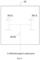
- the signal collection network 301 includes signal collection lines 301A and a synthesis unit 301B, the number of the signal collection lines 301A being the same as the number of the radio frequency signal output ports, the signal collection lines 301A being respectively located below different coupling holes 201, the signal collection lines 301A being respectively parallel to the corresponding first output feeders 102, and each of the signal collection lines 301A is connected to the synthesis unit 301B.
- An output port of the synthesis unit 301B serves as a calibration signal output port, and the calibration signal output port is connected to the processing system 40.
- the signal collection lines 301A are configured to collect coupling signals from the first output feeders 102 and transmit the collected coupling signals to the synthesis unit 301B.
- the synthesis unit 301B is configured to synthesize the received coupling signals to obtain a calibration signal and transmit the calibration signal to the processing system 40 via the calibration signal output port.
- the number of radio frequency signal output ports is equal to the number of first output feeders 102
- the number of coupling holes 201 is the same as the number of radio frequency signal output ports
- the number of signal collection lines 301A is the same as the number of radio frequency signal output ports, i.e., the number of the two is the same as the number of first output feeders 102.
- the radio frequency feed layer 10, the coupling layer 20, and the synthesis layer 30 are integrated monolithically.
- the monolithic integration is achieved through a radio frequency multilayer board, such as Rogers 4350. A process using monolithic integration provides better effects of integration.
- N sets of chips are provided on the first side of the radio frequency feed layer 10, radio frequency signal input ports of the N sets of chips are respectively connected to output ends of a 1-to-N splitter, and an input end of the 1-to-N splitter is connected to the processing system, where N is an integer multiple of 2.
- N is 4.
- the chip 101 includes four radio frequency signal output ports, and the four radio frequency signal output ports are respectively connected to four antenna units 50.
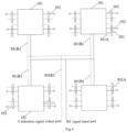
- the synthesis unit 301B includes N 4-way synthesizers 301B1 and one N-in-1 synthesizer 301B2, four signal collection lines 301A of a same se tare respectively connected to different input ends of the corresponding 4-way synthesizers 301B1, and output ends of the N 4-way synthesizers 301B1 are connected to different input ends of the N-in-1 synthesizer 301B2.
- An output end of the N-in-1 synthesizer 301B2 serves as a calibration signal output port, and the four signal collection lines 301A of a same set are four signal collection lines of a same chip 101 to which the corresponding first output feeders 102 are connected.
- the signal collection lines 301A have a same length and width as the corresponding first output feeders 102.
- the length of the coupling holes 201 is the same as the length of the first output feeders 102, and the width of the coupling holes 201 is preset to be proportional to the width of the first output feeders 102.
- the radio frequency signal output ports of the chips 101 are connected to corresponding antenna units 50 via corresponding first output feeders 102 and second output feeders passing through vertical holes 103.
- the radio frequency signal internal calibration system takes low-cost radio frequency boards as a carrier, and enables a complex internal calibration network through a multilayer board lamination process using a layer of coupling slotted structure (the coupling holes 201 in the coupling layer 20) and a layer of synthesis network (the signal collection network 301 in the synthesis layer 30). It has some advantages for the implementation of internal calibration of flat-panel phased array antennas. Firstly, the structure is small in size. A flat-panel phased array antenna is typically realized through a multilayer board lamination process, and newly adding an internal calibration network will typically result in increased complexities or processing difficulties, which is not conducive to the realization of the entire antenna.
- the embodiments of the present disclosure are carried out using a two-layer structure, which will not excessively increase the thickness and size of the structure, and is thus applicable to the implementation of communication solutions. Accordingly, it enables a relatively good control of the overall cost. Secondly, it has lower impacts on the original implementing architecture. The addition of an internal calibration network has lower impacts on the original radio frequency signal layer, and will not excessively deteriorate its power. By adjusting the slot size of the coupling holes 201, precise coupling amount control may be achieved, integration may be realized using a well-established multilayer board process, and it also achieves good consistency control among multiple channels.
- the radio frequency signal internal calibration system provided by embodiments of the present disclosure is primarily implemented at the internal calibration network of a flat-panel antenna, and by utilizing monolithic integration and a coupling slotted structure; it minimizes the influences on the original flat-panel antenna while having the advantage of higher integration.
- An embodiment of the present disclosure further provides a phased array antenna comprising an above-described radio frequency signal internal calibration system.
- the structure of the phased array antenna is as shown in FIG. 5 .
- phased array antenna according to the embodiment of the present disclosure includes the radio frequency signal internal calibration system in the foregoing embodiments, so that the phased array antenna may achieve the technical effects corresponding to the radio frequency signal internal calibration system in the foregoing embodiments.
- the processing system in the embodiments of the present disclosure may be an integrated circuit chip with signal processing capabilities.
- the processing system described above may be a general-purpose processor, including a Central Processing Unit (CPU), a Network Processor (NP), etc.; it may also be a Digital Signal Processor (DSP), an Application Specific Integrated Circuit (ASIC), a Field-Programmable Gate Array (FPGA), as well as other programmable logic devices, discrete gate or transistor logic devices, or discrete hardware components.
- CPU Central Processing Unit
- NP Network Processor
- DSP Digital Signal Processor
- ASIC Application Specific Integrated Circuit
- FPGA Field-Programmable Gate Array
Landscapes
- Physics & Mathematics (AREA)
- Electromagnetism (AREA)
- Engineering & Computer Science (AREA)
- Computer Networks & Wireless Communication (AREA)
- Signal Processing (AREA)
- Variable-Direction Aerials And Aerial Arrays (AREA)
Abstract
Description
- The present disclosure relates to the field of communications, and in particular, to a radio frequency signal internal calibration system and a phased array antenna.
- Flat-panel phased arrays enjoy numerous advantages such as flexible beam conversion, rapid scan switching, high reliability and light weight. In recent years, flat-panel phased arrays have been widely used in various types of civil communication systems and a variety of radar systems. Due to the complex structure of a phased array system and the large number of components, amplitude-phase characteristics of active radio frequency channels will change following prolonged use or storage, resulting in deterioration of the entire antenna. Therefore, flat-panel phased arrays need to be calibrated during operation to correct the amplitude-phase information.
- Current calibration methods typically employ near-field or far-field calibration, which poses certain challenges for working products. Frequently the technical conditions for near-field or far-field calibration are not available on site, and the near-field or far-field calibration is generally more time-consuming, labor-intensive, and expensive, which is not conducive to the maintenance of the products.
- It is an object of the present disclosure to provide a radio frequency signal internal calibration system and a phased array antenna to at least partially alleviate the issues mentioned above.
- In order to attain the object above, the technical solutions employed in the embodiments of the present disclosure are as follows.
- According to a first aspect, an embodiment of the present disclosure provides a radio frequency signal internal calibration system, comprising: a radio frequency feed layer, a coupling layer, a synthesis layer, and a processing system, the coupling layer being disposed between the radio frequency feed layer and the synthesis layer;
- The radio frequency feed layer is provided with an output feeder for outputting a signal to an antenna unit;
- The synthesis layer is provided with a signal collection network, the signal collection network being configured to collect coupling signals from corresponding output feeders, to synthesize the collected coupling signals to obtain a calibration signal, and to transmit the calibration signal to the processing system;
- The processing system determines whether calibration needs to be performed based on the calibration signal.
- In a possible implementation, at least one set of chips is provided on a first side of the radio frequency feed layer, the chip comprising one radio frequency signal input port and at least two radio frequency signal output ports, each radio frequency signal output port being connected to a corresponding antenna unit via a different output feeder, the first side of the radio frequency feed layer being a side of the radio frequency feed layer away from the coupling layer, the radio frequency signal input port being connected to the processing system;
- The coupling layer is provided with coupling holes, the number of the coupling holes being the same as the number of radio frequency signal output ports, the coupling holes being respectively located directly below different first output feeders, the first output feeders being output feeders connected to the radio frequency signal output ports and located on the first side of the radio frequency feed layer;
- The signal collection network comprises a signal collection line and a synthesis unit, the number of signal collection lines being the same as the number of radio frequency signal output ports, the signal collection lines being located directly below different coupling holes respectively, the signal collection lines being parallel to corresponding first output feeders respectively, the signal collection lines each being connected to the synthesis unit, an output port of the synthesis unit serving as a calibration signal output port, the calibration signal output port being connected to the processing system;
- The signal collection lines are configured to collect coupling signals from the first output feeders and transmit the collected coupling signals to the synthesis unit;
- The synthesis unit is configured to synthesize the received coupling signals to obtain a calibration signal, and transmit the calibration signal to the processing system via the calibration signal output port.
- In a possible implementation, the radio frequency feed layer, the coupling layer and the synthesis layer are monolithically integrated.
- In a possible implementation, the first side of the radio frequency feed layer is provided with N sets of chips, radio frequency signal input ports of the N sets of chips are respectively connected to output ends of a 1-to-N splitter, and an input end of the 1-to-N splitter is connected to the processing system, where N is an integer multiple of 2.
- In a possible implementation, the chip comprises 4 radio frequency signal output ports.
- In a possible implementation, the synthesis unit comprises N 4-way synthesizers and one N-in-1 synthesizer, four signal collection lines of a same set being respectively connected to different input ends of a corresponding 4-way synthesizer, output ends of the N 4-way synthesizers being connected to different input ends of the N-in-1 synthesizer, an output end of the N-in-1 synthesizer serving as the calibration signal output port, and the four signal collection lines of a same set are four signal collection lines of a same chip to which corresponding first output feeders are connected.
- In a possible implementation, the signal collection lines have a same length and width as the corresponding first output feeders.
- In a possible implementation, a length of the coupling holes is the same as a length of the first output feeders, and a width of the coupling holes is preset to be proportional to a width of the first output feeders.
- In a possible implementation, the radio frequency signal output ports are connected to corresponding antenna units via corresponding first output feeders and second output feeders passing through vertical holes.
- According to a second aspect, an embodiment of the present disclosure provides a phased array antenna, the phased array antenna comprising a radio frequency signal internal calibration system as described above.
- Relative to the prior art, embodiments of the present disclosure provide a radio frequency signal internal calibration system and a phased array antenna, the radio frequency signal internal calibration system comprising: a radio frequency feed layer, a coupling layer, a synthesis layer, and a processing system, wherein the coupling layer is disposed between the radio frequency feed layer and the synthesis layer, wherein the radio frequency feed layer is provided with an output feeder for outputting a signal to the antenna unit, wherein the synthesis layer is provided with a signal collection network, which is configured to collect in real time coupling signals from the corresponding output feeders, synthesize the collected coupling signals to obtain a calibration signal, and transmit the calibration signal to the processing system, and wherein the processing system determines whether calibration needs to be performed based on the calibration signal. The radio frequency signal internal calibration system provided by the present disclosure can achieve internal calibration in real time, which is easier to implement, less costly, less time-consuming and less labor-intensive, as compared to the far-field or near-field external calibration.
- In order to make the above objects, features and advantages of the present disclosure more apparent, preferred embodiments are exemplified below, and are described in detail as follows in conjunction with the accompanying drawings.
- In order to more clearly illustrate the technical solutions of the embodiments of the present disclosure, the accompanying drawings to be used in the embodiments will be briefly introduced below. It should be understood that the following figures are only illustrative of certain embodiments of the present disclosure, and therefore should not be regarded as limiting to its scope. For those skilled in the art, other related drawings could also be obtained from these drawings without exercise of any ingenuity.
-
FIG. 1 is a schematic diagram of a structure of a radio frequency signal internal calibration system according to an embodiment of the present disclosure; -
FIG. 2 shows schematically connection of a radio frequency signal internal calibration system according to an embodiment of the present disclosure; -
FIG. 3a shows schematically a structure of a radio frequency feed layer according to an embodiment of the present disclosure; -
FIG. 3b shows schematically a structure of a coupling layer according to an embodiment of the present disclosure; -
FIG. 3c shows schematically a structure of a synthesis layer according to an embodiment of the present disclosure; -
FIG. 4 is another schematic diagram of a structure of a radio frequency signal internal calibration system according to an embodiment of the present disclosure; and -
FIG. 5 shows schematically a structure of a phased array antenna according to an embodiment of the present disclosure. - Reference numbers in the figures include: 10-radio frequency feed layer; 101-chip; 102-first output feeder; 103-vertical hole; 20-coupling layer; 201-coupling hole; 30-synthesis layer; 301-signal collection network; 301A-signal collection line; 301B-synthesis unit; 301B1-4-way synthesizer; 301B2-N-in-1 synthesizer; 40-processing system; 50-Antenna unit.
- In order to make the objects, technical solutions and advantages of the embodiments of the present disclosure clearer, the technical solutions in the embodiments of the present disclosure will be clearly and completely described below in conjunction with the accompanying drawings. Apparently, the embodiments described herein are some, but not all, embodiments of the present disclosure. The components in the embodiments of the present disclosure described and illustrated herein may generally be arranged and designed in a variety of different configurations.
- Accordingly, the following detailed description of the embodiments of the present disclosure as provided in the accompanying drawings is not intended to limit the scope of the present disclosure, but merely to indicate selected embodiments of the present disclosure. Based on the embodiments in the present disclosure, all other embodiments obtained without exercise of ingenuity by a person of ordinary skill in the art fall within the scope of protection of the present disclosure.
- It should be noted that like reference numerals and letters refer to like items in the following figures, and thus, once an item is defined in one figure, it need not be further defined and explained in subsequent ones. Moreover, the terms "first", "second" and the like are herein used solely to distinguish one from another and are not to be construed as indicating or implying relative importance.
- It is to be noted that relational terms such as first and second herein are used only to distinguish one entity or operation from another, and do not necessarily require or imply any such actual relationship or order between those entities or operations. Furthermore, the terms "including", "comprising", or any other variant thereof, are intended to cover non-exclusive inclusion, such that a process, method, article, or apparatus comprising a set of elements includes not only those elements, but also other elements not expressly listed, or elements that are inherent to such process, method, article or apparatus. Without further limitation, the fact that an element is defined by the phrase "comprising a ......" does not preclude the existence of additional identical elements in the process, method, article or apparatus that comprises the element.
- In the description of the present disclosure, it should be noted that an orientation or a positional relationship indicated by such terms as "upper", "lower", "inner" and "outer", if any, is based on that shown in the drawings, or that of the product of the present disclosure as it is in use. This is only for ease and simplicity of description, without indicating or implying that the device or the element referred to must have a specific orientation, or be constructed and operated in a particular orientation, and thus it should not be construed as limiting to the present disclosure.
- In the description of the present disclosure, it should also be noted that, unless otherwise expressly specified or defined, the terms "provided" and "connected" and the like are to be understood in a broad sense. For example, it may be a fixed connection, a detachable connection, or an integral connection; it may be a mechanical connection or an electrical connection; it may be a direct connection, or an indirect connection through an intermediary, or an internal communication of two elements. For a person of ordinary skill in the art, the specific meanings of these terms in the present disclosure may be understood in specific contexts.
- Some embodiments of the present disclosure are described in detail below in conjunction with the accompanying drawings. The following embodiments and features therein may be combined with each other in the absence of conflicts.
- Current calibration methods typically employ near-field or far-field calibration, which poses certain challenges for working products. Frequently the technical conditions for near-field or far-field calibration are not available on site, and the near-field or far-field calibration is generally more time-consuming, labor-intensive, and expensive, which is not conducive to the maintenance of the products.
- To address the above issues, an embodiment of the present disclosure proposes a radio frequency signal internal calibration system. As shown in
FIG. 1 , the radio frequency signal internal calibration system includes: a radiofrequency feed layer 10, acoupling layer 20, asynthesis layer 30, and aprocessing system 40, with thecoupling layer 20 disposed between the radiofrequency feed layer 10 and thesynthesis layer 30. - The radio
frequency feed layer 10 is provided with an output feeder for outputting a signal to anantenna unit 50. - The
synthesis layer 30 is provided with asignal collection network 301, and thesignal collection network 301 is configured to collect coupling signals from corresponding output feeders, synthesize the collected coupling signals to obtain a calibration signal, and transmit the calibration signal to theprocessing system 40. - As shown in
FIG. 2 , thesignal collection network 301 is communicatively connected to theprocessing system 40. - The
processing system 40 determines whether calibration needs to be performed based on the calibration signal. - In summary, embodiments of the present disclosure provide a radio frequency signal internal calibration system, the radio frequency signal internal calibration system comprising: a radio frequency feed layer, a coupling layer, a synthesis layer, and a processing system; the coupling layer being disposed between the radio frequency feed layer and the synthesis layer; the radio frequency feed layer being provided with an output feeder for outputting a signal to an antenna unit; the synthesis layer being provided with a signal collection network, which is configured to collect in real time coupling signals from corresponding output feeders, synthesize the collected coupling signals to obtain a calibration signal, and transmit the calibration signal to the processing system; and the processing system determining whether calibration needs to be performed based on the calibration signal. The radio frequency signal internal calibration system provided by the present disclosure can achieve internal calibration in real time, which is easier to implement, less costly, less time-consuming and less labor-intensive, as compared to the far-field or near-field external calibration.
- Referring to
FIGS. 3a, 3b , and3c on the basis ofFIG. 1 , embodiments of the present disclosure further provide possible structures of the radiofrequency feed layer 10, thecoupling layer 20, and thesynthesis layer 30. - As shown in
FIG. 3a , at least one set ofchips 101 is provided on a first side of the radiofrequency feed layer 10, thechip 101 comprising one radio frequency signal input port and at least two radio frequency signal output ports, each of the radio frequency signal output ports being connected to acorresponding antenna unit 50 via a different output feeder, the first side of the radiofrequency feed layer 10 beinga side of the radiofrequency feed layer 10 away from thecoupling layer 20, and the radio frequency signal input port is connected to theprocessing system 40. - Optionally, the
chip 101 may implement signal distribution, distributing input signals from the radio frequency signal input port, perform amplitude and phase modulation of the distributed signals within thechip 101, and output the modulated signals to acorresponding antenna unit 50 via the radio frequency signal output ports. - As shown in
FIG. 3b , thecoupling layer 20 is provided withcoupling holes 201, the number ofcoupling holes 201 being the same as the number of radio frequency signal output ports, the coupling holes 201 being each located directly below differentfirst output feeders 102, thefirst output feeders 102 being output feeders that are coupled to the radio frequency signal output ports and located on the first side of the radiofrequency feed layer 10. - As shown in
FIG. 3c , thesignal collection network 301 includessignal collection lines 301A and asynthesis unit 301B, the number of thesignal collection lines 301A being the same as the number of the radio frequency signal output ports, thesignal collection lines 301A being respectively located belowdifferent coupling holes 201, thesignal collection lines 301A being respectively parallel to the correspondingfirst output feeders 102, and each of thesignal collection lines 301A is connected to thesynthesis unit 301B. An output port of thesynthesis unit 301B serves as a calibration signal output port, and the calibration signal output port is connected to theprocessing system 40. - The
signal collection lines 301A are configured to collect coupling signals from thefirst output feeders 102 and transmit the collected coupling signals to thesynthesis unit 301B. - The
synthesis unit 301B is configured to synthesize the received coupling signals to obtain a calibration signal and transmit the calibration signal to theprocessing system 40 via the calibration signal output port. - It should be noted that the number of radio frequency signal output ports is equal to the number of
first output feeders 102, the number of coupling holes 201 is the same as the number of radio frequency signal output ports, and the number ofsignal collection lines 301A is the same as the number of radio frequency signal output ports, i.e., the number of the two is the same as the number offirst output feeders 102. - In a possible implementation, the radio
frequency feed layer 10, thecoupling layer 20, and thesynthesis layer 30 are integrated monolithically. Optionally, the monolithic integration is achieved through a radio frequency multilayer board, such as Rogers 4350. A process using monolithic integration provides better effects of integration. - In a possible implementation, N sets of chips are provided on the first side of the radio
frequency feed layer 10, radio frequency signal input ports of the N sets of chips are respectively connected to output ends of a 1-to-N splitter, and an input end of the 1-to-N splitter is connected to the processing system, where N is an integer multiple of 2. Optionally, N is 4. - Referring to
FIG. 4 , in a possible implementation, thechip 101 includes four radio frequency signal output ports, and the four radio frequency signal output ports are respectively connected to fourantenna units 50. - Still referring to
FIG. 4 , thesynthesis unit 301B includes N 4-way synthesizers 301B1 and one N-in-1 synthesizer 301B2, foursignal collection lines 301A of a same se tare respectively connected to different input ends of the corresponding 4-way synthesizers 301B1, and output ends of the N 4-way synthesizers 301B1 are connected to different input ends of the N-in-1 synthesizer 301B2. An output end of the N-in-1 synthesizer 301B2 serves as a calibration signal output port, and the foursignal collection lines 301A of a same set are four signal collection lines of asame chip 101 to which the correspondingfirst output feeders 102 are connected. - In a possible implementation, the
signal collection lines 301A have a same length and width as the correspondingfirst output feeders 102. - In a possible implementation, the length of the coupling holes 201 is the same as the length of the
first output feeders 102, and the width of the coupling holes 201 is preset to be proportional to the width of thefirst output feeders 102. - Referring to
FIG. 5 , in a possible implementation, the radio frequency signal output ports of thechips 101 are connected to correspondingantenna units 50 via correspondingfirst output feeders 102 and second output feeders passing throughvertical holes 103. - The radio frequency signal internal calibration system provided in the embodiments of the present disclosure takes low-cost radio frequency boards as a carrier, and enables a complex internal calibration network through a multilayer board lamination process using a layer of coupling slotted structure (the coupling holes 201 in the coupling layer 20) and a layer of synthesis network (the
signal collection network 301 in the synthesis layer 30). It has some advantages for the implementation of internal calibration of flat-panel phased array antennas. Firstly, the structure is small in size. A flat-panel phased array antenna is typically realized through a multilayer board lamination process, and newly adding an internal calibration network will typically result in increased complexities or processing difficulties, which is not conducive to the realization of the entire antenna. The embodiments of the present disclosure are carried out using a two-layer structure, which will not excessively increase the thickness and size of the structure, and is thus applicable to the implementation of communication solutions. Accordingly, it enables a relatively good control of the overall cost. Secondly, it has lower impacts on the original implementing architecture. The addition of an internal calibration network has lower impacts on the original radio frequency signal layer, and will not excessively deteriorate its power. By adjusting the slot size of the coupling holes 201, precise coupling amount control may be achieved, integration may be realized using a well-established multilayer board process, and it also achieves good consistency control among multiple channels. The radio frequency signal internal calibration system provided by embodiments of the present disclosure is primarily implemented at the internal calibration network of a flat-panel antenna, and by utilizing monolithic integration and a coupling slotted structure; it minimizes the influences on the original flat-panel antenna while having the advantage of higher integration. - An embodiment of the present disclosure further provides a phased array antenna comprising an above-described radio frequency signal internal calibration system. The structure of the phased array antenna is as shown in
FIG. 5 . - It is to be noted that the phased array antenna according to the embodiment of the present disclosure includes the radio frequency signal internal calibration system in the foregoing embodiments, so that the phased array antenna may achieve the technical effects corresponding to the radio frequency signal internal calibration system in the foregoing embodiments. For the sake of brevity, reference may be made to the above disclosure for whatever is not mentioned in this embodiment.
- The processing system in the embodiments of the present disclosure may be an integrated circuit chip with signal processing capabilities. The processing system described above may be a general-purpose processor, including a Central Processing Unit (CPU), a Network Processor (NP), etc.; it may also be a Digital Signal Processor (DSP), an Application Specific Integrated Circuit (ASIC), a Field-Programmable Gate Array (FPGA), as well as other programmable logic devices, discrete gate or transistor logic devices, or discrete hardware components.
- The foregoing are only preferred embodiments of the present disclosure, which are not intended to limit the present disclosure but are subject to various modifications or changes for those skilled in the art. Any modifications, equivalent substitutions, improvements or the like made within the spirit and principle of the present disclosure shall be included in the scope of present disclosure.
- It is apparent to those skilled in the art that the present disclosure is not limited to the details of the exemplary embodiments described above, and that the present disclosure may be otherwise enabled in other specific forms without departing from the spirit or essential features of the present disclosure. Accordingly, the embodiments are to be regarded as exemplary and non-limiting in each and every point of view, and the scope of the present disclosure is defined by the appended claims and not by the foregoing description, and is therefore intended to encompass all changes falling within the meaning and scope of equivalents to the claims. Any reference sign in a claim should not be construed as limiting the claim concerned.
Claims (9)
- A radio frequency signal internal calibration system, comprising: a radio frequency feed layer, a coupling layer, a synthesis layer, and a processing system, the coupling layer being disposed between the radio frequency feed layer and the synthesis layer,wherein the radio frequency feed layer is provided with an output feeder for outputting a signal to an antenna unit;wherein the synthesis layer is provided with a signal collection network configured to collect coupling signals from corresponding output feeders, to synthesize the collected coupling signals to obtain a calibration signal, and to transmit the calibration signal to the processing system;wherein the processing system determines whether calibration needs to be performed based on the calibration signal;wherein at least one set of chips is provided on a first side of the radio frequency feed layer, the chip comprising one radio frequency signal input port and at least two radio frequency signal output ports, each radio frequency signal output port being connected to a corresponding antenna unit via a different output feeder, the first side of the radio frequency feed layer being a side of the radio frequency feed layer away from the coupling layer, the radio frequency signal input port being connected to the processing system;wherein the coupling layer is provided with coupling holes, the number of the coupling holes being the same as the number of radio frequency signal output ports, the coupling holes being respectively located directly below different first output feeders, the first output feeders being output feeders connected to the radio frequency signal output ports and located on the first side of the radio frequency feed layer;wherein the signal collection network comprises a signal collection line and a synthesis unit, the number of signal collection lines being the same as the number of radio frequency signal output ports, the signal collection lines being located directly below different coupling holes respectively, the signal collection lines being parallel to corresponding first output feeders respectively, the signal collection lines each being connected to the synthesis unit, an output port of the synthesis unit serving as a calibration signal output port, the calibration signal output port being connected to the processing system;wherein the signal collection lines are configured to collect coupling signals from the first output feeders and transmit the collected coupling signals to the synthesis unit; andwherein the synthesis unit is configured to synthesize the received coupling signals to obtain a calibration signal, and transmit the calibration signal to the processing system via the calibration signal output port.
- The radio frequency signal internal calibration system according to claim 1, wherein the radio frequency feed layer, the coupling layer and the synthesis layer are monolithically integrated.
- The radio frequency signal internal calibration system according to claim 1, wherein the first side of the radio frequency feed layer is provided with N sets of chips, radio frequency signal input ports of the N sets of chips being respectively connected to output ends of a 1-to-N splitter, an input end of the 1-to-N splitter being connected to the processing system, where N is an integer multiple of 2.
- The radio frequency signal internal calibration system according to claim 3, wherein the chip comprises 4 radio frequency signal output ports.
- The radio frequency signal internal calibration system according to claim 4, wherein the synthesis unit comprises N 4-way synthesizers and one N-in-1 synthesizer, four signal collection lines of a same set being respectively connected to different input ends of a corresponding 4-way synthesizer, output ends of the N 4-way synthesizers being connected to different input ends of the N-in-1 synthesizer, an output end of the N-in-1 synthesizer serving as the calibration signal output port, and wherein the four signal collection lines of a same set are four signal collection lines of a same chip to which corresponding first output feeders are connected.
- The radio frequency signal internal calibration system according to claim 1, wherein the signal collection lines have a same length and width as the corresponding first output feeders.
- The radio frequency signal internal calibration system according to claim 6, wherein a length of the coupling holes is the same as a length of the first output feeders, and wherein a width of the coupling holes is preset to be proportional to a width of the first output feeders.
- The radio frequency signal internal calibration system according to claim 1, wherein the radio frequency signal output ports are connected to corresponding antenna units via corresponding first output feeders and second output feeders passing through vertical holes.
- A phased array antenna comprising a radio frequency signal internal calibration system according to any one of claims 1 to 8.
Applications Claiming Priority (2)
| Application Number | Priority Date | Filing Date | Title |
|---|---|---|---|
| CN202110549314.7A CN112994808B (en) | 2021-05-20 | 2021-05-20 | Radio frequency signal internal calibration system and phased array antenna |
| PCT/CN2022/091732 WO2022242492A1 (en) | 2021-05-20 | 2022-05-09 | Radio frequency signal internal calibration system and phased array antenna |
Publications (4)
| Publication Number | Publication Date |
|---|---|
| EP4325748A1 true EP4325748A1 (en) | 2024-02-21 |
| EP4325748A4 EP4325748A4 (en) | 2024-07-03 |
| EP4325748C0 EP4325748C0 (en) | 2025-12-31 |
| EP4325748B1 EP4325748B1 (en) | 2025-12-31 |
Family
ID=76337141
Family Applications (1)
| Application Number | Title | Priority Date | Filing Date |
|---|---|---|---|
| EP22803814.7A Active EP4325748B1 (en) | 2021-05-20 | 2022-05-09 | SYSTEM FOR INTERNAL CALIBRATION OF A RADIO FREQUENCY SIGNAL AND PHASE-CONTROLLED GROUP ANTENNA |
Country Status (3)
| Country | Link |
|---|---|
| EP (1) | EP4325748B1 (en) |
| CN (1) | CN112994808B (en) |
| WO (1) | WO2022242492A1 (en) |
Families Citing this family (5)
| Publication number | Priority date | Publication date | Assignee | Title |
|---|---|---|---|---|
| CN112994808B (en) * | 2021-05-20 | 2021-07-27 | 成都天锐星通科技有限公司 | Radio frequency signal internal calibration system and phased array antenna |
| CN115693075B (en) * | 2022-10-17 | 2025-07-15 | 华南理工大学 | Broadband Antenna Calibration Network Based on Multilayer Coupling Technology |
| CN116545548A (en) * | 2023-04-13 | 2023-08-04 | 中国电子科技集团公司第二十研究所 | Sandwich type internal calibration structure integrated inside multichannel compact T/R assembly |
| CN117192501B (en) * | 2023-09-28 | 2024-05-17 | 广州中雷电科科技有限公司 | Phased array system calibration monitoring device, system and method |
| CN120127386B (en) * | 2025-03-31 | 2025-11-18 | 中国电子科技集团公司第三十八研究所 | A slot-coupled feed phased array thin-film antenna with correction function |
Family Cites Families (12)
| Publication number | Priority date | Publication date | Assignee | Title |
|---|---|---|---|---|
| FR2960100B1 (en) * | 2010-05-12 | 2013-02-15 | Thales Sa | CALIBRATIONS OF AN ELECTRONIC SCANNING ANTENNA COMPRISING A NETWORK OF RADIANT ELEMENTS |
| CN103353904B (en) * | 2013-04-12 | 2016-04-27 | 西安电子科技大学 | Active interlayer microstrip antenna and the comprehensive data-driven method for designing of electromagnetism and antenna |
| CN103997352B (en) * | 2014-05-14 | 2016-02-24 | 电信科学技术研究院 | Active antenna related equipment, system and method for transmitting and receiving calibration |
| CN104506253A (en) * | 2015-01-13 | 2015-04-08 | 重庆大学 | Amplitude phase error correction system and method for transmitting channel of phased-array antenna |
| CN104954083B (en) * | 2015-06-16 | 2018-05-29 | 上海华为技术有限公司 | The method, apparatus and system of a kind of antenna array calibration |
| CN105390814B (en) * | 2015-10-18 | 2018-06-26 | 中国电子科技集团公司第十研究所 | Active phase array antenna with internal calibration network |
| CN107959533B (en) * | 2016-10-17 | 2020-11-06 | 华为技术有限公司 | Wireless device and radio frequency channel calibration method |
| WO2020006748A1 (en) * | 2018-07-06 | 2020-01-09 | 华为技术有限公司 | Method for calibrating phased-array antenna, and related apparatus |
| CN110190387A (en) * | 2019-05-08 | 2019-08-30 | 成都天锐星通科技有限公司 | A kind of single feedback double-circle polarization microstrip antenna |
| CN111276812B (en) * | 2020-03-16 | 2024-07-26 | 成都天锐星通科技有限公司 | A multi-layer microstrip antenna array element and antenna array surface |
| CN212626071U (en) * | 2020-09-18 | 2021-02-26 | 成都天锐星通科技有限公司 | Phased array antenna and communication equipment |
| CN112994808B (en) * | 2021-05-20 | 2021-07-27 | 成都天锐星通科技有限公司 | Radio frequency signal internal calibration system and phased array antenna |
-
2021
- 2021-05-20 CN CN202110549314.7A patent/CN112994808B/en active Active
-
2022
- 2022-05-09 EP EP22803814.7A patent/EP4325748B1/en active Active
- 2022-05-09 WO PCT/CN2022/091732 patent/WO2022242492A1/en not_active Ceased
Also Published As
| Publication number | Publication date |
|---|---|
| CN112994808A (en) | 2021-06-18 |
| EP4325748C0 (en) | 2025-12-31 |
| EP4325748B1 (en) | 2025-12-31 |
| CN112994808B (en) | 2021-07-27 |
| WO2022242492A1 (en) | 2022-11-24 |
| EP4325748A4 (en) | 2024-07-03 |
Similar Documents
| Publication | Publication Date | Title |
|---|---|---|
| EP4325748A1 (en) | Radio frequency signal internal calibration system and phased array antenna | |
| US10530053B2 (en) | System and method for measuring a plurality of RF signal paths | |
| DK2117077T3 (en) | radar Antenna | |
| CN114902493B (en) | Phased Array Module | |
| CN109155459A (en) | Suitable for the antenna element and device by selectively coupled device line and the AAS of TRX RF subgroup calibration | |
| US20210005981A1 (en) | Array antenna | |
| CN109632046B (en) | Radar level gauge with synchronization signals on different circuit board layers | |
| CN108963459A (en) | A kind of measurement method and equipment | |
| CN101479884A (en) | receiver unit and transmitter unit | |
| EP3985888B1 (en) | Method for calibrating transmitter-to-receiver relative phase in millimeter wave beamforming system and associated beamforming system | |
| CN109632047A (en) | Radar level gauge with high-frequency amplifier | |
| US20190067770A1 (en) | Antenna apparatus including phase shifter | |
| US11177581B2 (en) | Multi-chip system for an antenna array | |
| US20230261374A1 (en) | Mimo antenna system and method | |
| CN110198172A (en) | A kind of calibration network and antenna for base station of array antenna | |
| CN105846057A (en) | GNSS atmosphere spaceborne occultation antenna designed in mode of spaceborne bias beams | |
| CN110024221A (en) | Coherent signal is distributed to big electrical distance by serial interlinkage | |
| JP2019186717A (en) | Array antenna system and calibration method for array antenna system | |
| CN211376936U (en) | A Microstrip Phased Array Antenna Based on DDS | |
| EP4005027B1 (en) | Base station antenna and base station | |
| CN113424366B (en) | Method and system for signal self-alignment in large-scale phased array systems | |
| Wane et al. | Cognitive beamformer chips with smart-antennas for 5G and beyond: Holistic RFSOI technology solutions including ASIC correlators | |
| USH2028H1 (en) | Frequency-scan traveling wave antenna | |
| JP2000223924A (en) | Antenna device | |
| CN107645044A (en) | Rectangle wave beam communication base station antenna |
Legal Events
| Date | Code | Title | Description |
|---|---|---|---|
| STAA | Information on the status of an ep patent application or granted ep patent |
Free format text: STATUS: THE INTERNATIONAL PUBLICATION HAS BEEN MADE |
|
| PUAI | Public reference made under article 153(3) epc to a published international application that has entered the european phase |
Free format text: ORIGINAL CODE: 0009012 |
|
| STAA | Information on the status of an ep patent application or granted ep patent |
Free format text: STATUS: REQUEST FOR EXAMINATION WAS MADE |
|
| 17P | Request for examination filed |
Effective date: 20231114 |
|
| AK | Designated contracting states |
Kind code of ref document: A1 Designated state(s): AL AT BE BG CH CY CZ DE DK EE ES FI FR GB GR HR HU IE IS IT LI LT LU LV MC MK MT NL NO PL PT RO RS SE SI SK SM TR |
|
| A4 | Supplementary search report drawn up and despatched |
Effective date: 20240604 |
|
| RIC1 | Information provided on ipc code assigned before grant |
Ipc: H04B 17/00 20150101ALI20240528BHEP Ipc: H01Q 3/24 20060101ALI20240528BHEP Ipc: H01Q 1/38 20060101ALI20240528BHEP Ipc: H01Q 21/00 20060101ALI20240528BHEP Ipc: H04B 17/21 20150101ALI20240528BHEP Ipc: H04B 17/11 20150101AFI20240528BHEP |
|
| DAV | Request for validation of the european patent (deleted) | ||
| DAX | Request for extension of the european patent (deleted) | ||
| REG | Reference to a national code |
Ref country code: DE Free format text: PREVIOUS MAIN CLASS: H04B0017110000 Ref country code: DE Ref legal event code: R079 Ref document number: 602022028014 Country of ref document: DE Free format text: PREVIOUS MAIN CLASS: H04B0017110000 Ipc: H01Q0003240000 |
|
| GRAP | Despatch of communication of intention to grant a patent |
Free format text: ORIGINAL CODE: EPIDOSNIGR1 |
|
| STAA | Information on the status of an ep patent application or granted ep patent |
Free format text: STATUS: GRANT OF PATENT IS INTENDED |
|
| RIC1 | Information provided on ipc code assigned before grant |
Ipc: H04B 17/11 20150101ALI20250528BHEP Ipc: H04B 17/00 20150101ALI20250528BHEP Ipc: H01Q 3/24 20060101AFI20250528BHEP |
|
| INTG | Intention to grant announced |
Effective date: 20250613 |
|
| GRAS | Grant fee paid |
Free format text: ORIGINAL CODE: EPIDOSNIGR3 |
|
| GRAA | (expected) grant |
Free format text: ORIGINAL CODE: 0009210 |
|
| STAA | Information on the status of an ep patent application or granted ep patent |
Free format text: STATUS: THE PATENT HAS BEEN GRANTED |
|
| AK | Designated contracting states |
Kind code of ref document: B1 Designated state(s): AL AT BE BG CH CY CZ DE DK EE ES FI FR GB GR HR HU IE IS IT LI LT LU LV MC MK MT NL NO PL PT RO RS SE SI SK SM TR |
|
| REG | Reference to a national code |
Ref country code: CH Ref legal event code: F10 Free format text: ST27 STATUS EVENT CODE: U-0-0-F10-F00 (AS PROVIDED BY THE NATIONAL OFFICE) Effective date: 20251231 Ref country code: GB Ref legal event code: FG4D |
|
| REG | Reference to a national code |
Ref country code: DE Ref legal event code: R096 Ref document number: 602022028014 Country of ref document: DE |
|
| REG | Reference to a national code |
Ref country code: IE Ref legal event code: FG4D |
|
| U01 | Request for unitary effect filed |
Effective date: 20260114 |
|
| U07 | Unitary effect registered |
Designated state(s): AT BE BG DE DK EE FI FR IT LT LU LV MT NL PT RO SE SI Effective date: 20260121 |
|
| U20 | Renewal fee for the european patent with unitary effect paid |
Year of fee payment: 5 Effective date: 20260302 |
|
| PG25 | Lapsed in a contracting state [announced via postgrant information from national office to epo] |
Ref country code: NO Free format text: LAPSE BECAUSE OF FAILURE TO SUBMIT A TRANSLATION OF THE DESCRIPTION OR TO PAY THE FEE WITHIN THE PRESCRIBED TIME-LIMIT Effective date: 20260331 |
|
| PG25 | Lapsed in a contracting state [announced via postgrant information from national office to epo] |
Ref country code: HR Free format text: LAPSE BECAUSE OF FAILURE TO SUBMIT A TRANSLATION OF THE DESCRIPTION OR TO PAY THE FEE WITHIN THE PRESCRIBED TIME-LIMIT Effective date: 20251231 |
|
| PG25 | Lapsed in a contracting state [announced via postgrant information from national office to epo] |
Ref country code: RS Free format text: LAPSE BECAUSE OF FAILURE TO SUBMIT A TRANSLATION OF THE DESCRIPTION OR TO PAY THE FEE WITHIN THE PRESCRIBED TIME-LIMIT Effective date: 20260331 |