EP4325705A2 - Method for operating a power converter - Google Patents
Method for operating a power converter Download PDFInfo
- Publication number
- EP4325705A2 EP4325705A2 EP24150636.9A EP24150636A EP4325705A2 EP 4325705 A2 EP4325705 A2 EP 4325705A2 EP 24150636 A EP24150636 A EP 24150636A EP 4325705 A2 EP4325705 A2 EP 4325705A2
- Authority
- EP
- European Patent Office
- Prior art keywords
- voltage
- power converter
- common mode
- link
- input
- Prior art date
- Legal status (The legal status is an assumption and is not a legal conclusion. Google has not performed a legal analysis and makes no representation as to the accuracy of the status listed.)
- Pending
Links
Images











Classifications
-
- H—ELECTRICITY
- H02—GENERATION; CONVERSION OR DISTRIBUTION OF ELECTRIC POWER
- H02M—APPARATUS FOR CONVERSION BETWEEN AC AND AC, BETWEEN AC AND DC, OR BETWEEN DC AND DC, AND FOR USE WITH MAINS OR SIMILAR POWER SUPPLY SYSTEMS; CONVERSION OF DC OR AC INPUT POWER INTO SURGE OUTPUT POWER; CONTROL OR REGULATION THEREOF
- H02M1/00—Details of apparatus for conversion
- H02M1/42—Circuits or arrangements for compensating for or adjusting power factor in converters or inverters
- H02M1/4208—Arrangements for improving power factor of AC input
- H02M1/4216—Arrangements for improving power factor of AC input operating from a three-phase input voltage
-
- H—ELECTRICITY
- H02—GENERATION; CONVERSION OR DISTRIBUTION OF ELECTRIC POWER
- H02M—APPARATUS FOR CONVERSION BETWEEN AC AND AC, BETWEEN AC AND DC, OR BETWEEN DC AND DC, AND FOR USE WITH MAINS OR SIMILAR POWER SUPPLY SYSTEMS; CONVERSION OF DC OR AC INPUT POWER INTO SURGE OUTPUT POWER; CONTROL OR REGULATION THEREOF
- H02M7/00—Conversion of AC power input into DC power output; Conversion of DC power input into AC power output
- H02M7/02—Conversion of AC power input into DC power output without possibility of reversal
- H02M7/04—Conversion of AC power input into DC power output without possibility of reversal by static converters
- H02M7/12—Conversion of AC power input into DC power output without possibility of reversal by static converters using discharge tubes with control electrode or semiconductor devices with control electrode
- H02M7/21—Conversion of AC power input into DC power output without possibility of reversal by static converters using discharge tubes with control electrode or semiconductor devices with control electrode using devices of a triode or transistor type requiring continuous application of a control signal
- H02M7/217—Conversion of AC power input into DC power output without possibility of reversal by static converters using discharge tubes with control electrode or semiconductor devices with control electrode using devices of a triode or transistor type requiring continuous application of a control signal using semiconductor devices only
- H02M7/219—Conversion of AC power input into DC power output without possibility of reversal by static converters using discharge tubes with control electrode or semiconductor devices with control electrode using devices of a triode or transistor type requiring continuous application of a control signal using semiconductor devices only in a bridge configuration
-
- H—ELECTRICITY
- H02—GENERATION; CONVERSION OR DISTRIBUTION OF ELECTRIC POWER
- H02M—APPARATUS FOR CONVERSION BETWEEN AC AND AC, BETWEEN AC AND DC, OR BETWEEN DC AND DC, AND FOR USE WITH MAINS OR SIMILAR POWER SUPPLY SYSTEMS; CONVERSION OF DC OR AC INPUT POWER INTO SURGE OUTPUT POWER; CONTROL OR REGULATION THEREOF
- H02M1/00—Details of apparatus for conversion
- H02M1/12—Arrangements for reducing harmonics from AC input or output
-
- H—ELECTRICITY
- H02—GENERATION; CONVERSION OR DISTRIBUTION OF ELECTRIC POWER
- H02M—APPARATUS FOR CONVERSION BETWEEN AC AND AC, BETWEEN AC AND DC, OR BETWEEN DC AND DC, AND FOR USE WITH MAINS OR SIMILAR POWER SUPPLY SYSTEMS; CONVERSION OF DC OR AC INPUT POWER INTO SURGE OUTPUT POWER; CONTROL OR REGULATION THEREOF
- H02M7/00—Conversion of AC power input into DC power output; Conversion of DC power input into AC power output
- H02M7/02—Conversion of AC power input into DC power output without possibility of reversal
- H02M7/04—Conversion of AC power input into DC power output without possibility of reversal by static converters
- H02M7/12—Conversion of AC power input into DC power output without possibility of reversal by static converters using discharge tubes with control electrode or semiconductor devices with control electrode
- H02M7/21—Conversion of AC power input into DC power output without possibility of reversal by static converters using discharge tubes with control electrode or semiconductor devices with control electrode using devices of a triode or transistor type requiring continuous application of a control signal
- H02M7/217—Conversion of AC power input into DC power output without possibility of reversal by static converters using discharge tubes with control electrode or semiconductor devices with control electrode using devices of a triode or transistor type requiring continuous application of a control signal using semiconductor devices only
-
- H—ELECTRICITY
- H02—GENERATION; CONVERSION OR DISTRIBUTION OF ELECTRIC POWER
- H02M—APPARATUS FOR CONVERSION BETWEEN AC AND AC, BETWEEN AC AND DC, OR BETWEEN DC AND DC, AND FOR USE WITH MAINS OR SIMILAR POWER SUPPLY SYSTEMS; CONVERSION OF DC OR AC INPUT POWER INTO SURGE OUTPUT POWER; CONTROL OR REGULATION THEREOF
- H02M7/00—Conversion of AC power input into DC power output; Conversion of DC power input into AC power output
- H02M7/42—Conversion of DC power input into AC power output without possibility of reversal
- H02M7/44—Conversion of DC power input into AC power output without possibility of reversal by static converters
- H02M7/48—Conversion of DC power input into AC power output without possibility of reversal by static converters using discharge tubes with control electrode or semiconductor devices with control electrode
- H02M7/483—Converters with outputs that each can have more than two voltages levels
- H02M7/487—Neutral point clamped inverters
-
- H—ELECTRICITY
- H02—GENERATION; CONVERSION OR DISTRIBUTION OF ELECTRIC POWER
- H02M—APPARATUS FOR CONVERSION BETWEEN AC AND AC, BETWEEN AC AND DC, OR BETWEEN DC AND DC, AND FOR USE WITH MAINS OR SIMILAR POWER SUPPLY SYSTEMS; CONVERSION OF DC OR AC INPUT POWER INTO SURGE OUTPUT POWER; CONTROL OR REGULATION THEREOF
- H02M1/00—Details of apparatus for conversion
- H02M1/0048—Circuits or arrangements for reducing losses
-
- H—ELECTRICITY
- H02—GENERATION; CONVERSION OR DISTRIBUTION OF ELECTRIC POWER
- H02M—APPARATUS FOR CONVERSION BETWEEN AC AND AC, BETWEEN AC AND DC, OR BETWEEN DC AND DC, AND FOR USE WITH MAINS OR SIMILAR POWER SUPPLY SYSTEMS; CONVERSION OF DC OR AC INPUT POWER INTO SURGE OUTPUT POWER; CONTROL OR REGULATION THEREOF
- H02M1/00—Details of apparatus for conversion
- H02M1/0048—Circuits or arrangements for reducing losses
- H02M1/0054—Transistor switching losses
-
- H—ELECTRICITY
- H02—GENERATION; CONVERSION OR DISTRIBUTION OF ELECTRIC POWER
- H02M—APPARATUS FOR CONVERSION BETWEEN AC AND AC, BETWEEN AC AND DC, OR BETWEEN DC AND DC, AND FOR USE WITH MAINS OR SIMILAR POWER SUPPLY SYSTEMS; CONVERSION OF DC OR AC INPUT POWER INTO SURGE OUTPUT POWER; CONTROL OR REGULATION THEREOF
- H02M1/00—Details of apparatus for conversion
- H02M1/0067—Converter structures employing plural converter units, other than for parallel operation of the units on a single load
- H02M1/007—Plural converter units in cascade
-
- H—ELECTRICITY
- H02—GENERATION; CONVERSION OR DISTRIBUTION OF ELECTRIC POWER
- H02M—APPARATUS FOR CONVERSION BETWEEN AC AND AC, BETWEEN AC AND DC, OR BETWEEN DC AND DC, AND FOR USE WITH MAINS OR SIMILAR POWER SUPPLY SYSTEMS; CONVERSION OF DC OR AC INPUT POWER INTO SURGE OUTPUT POWER; CONTROL OR REGULATION THEREOF
- H02M1/00—Details of apparatus for conversion
- H02M1/0067—Converter structures employing plural converter units, other than for parallel operation of the units on a single load
- H02M1/0074—Plural converter units whose inputs are connected in series
-
- H—ELECTRICITY
- H02—GENERATION; CONVERSION OR DISTRIBUTION OF ELECTRIC POWER
- H02M—APPARATUS FOR CONVERSION BETWEEN AC AND AC, BETWEEN AC AND DC, OR BETWEEN DC AND DC, AND FOR USE WITH MAINS OR SIMILAR POWER SUPPLY SYSTEMS; CONVERSION OF DC OR AC INPUT POWER INTO SURGE OUTPUT POWER; CONTROL OR REGULATION THEREOF
- H02M1/00—Details of apparatus for conversion
- H02M1/0067—Converter structures employing plural converter units, other than for parallel operation of the units on a single load
- H02M1/0077—Plural converter units whose outputs are connected in series
-
- Y—GENERAL TAGGING OF NEW TECHNOLOGICAL DEVELOPMENTS; GENERAL TAGGING OF CROSS-SECTIONAL TECHNOLOGIES SPANNING OVER SEVERAL SECTIONS OF THE IPC; TECHNICAL SUBJECTS COVERED BY FORMER USPC CROSS-REFERENCE ART COLLECTIONS [XRACs] AND DIGESTS
- Y02—TECHNOLOGIES OR APPLICATIONS FOR MITIGATION OR ADAPTATION AGAINST CLIMATE CHANGE
- Y02B—CLIMATE CHANGE MITIGATION TECHNOLOGIES RELATED TO BUILDINGS, e.g. HOUSING, HOUSE APPLIANCES OR RELATED END-USER APPLICATIONS
- Y02B70/00—Technologies for an efficient end-user side electric power management and consumption
- Y02B70/10—Technologies improving the efficiency by using switched-mode power supplies [SMPS], i.e. efficient power electronics conversion e.g. power factor correction or reduction of losses in power supplies or efficient standby modes
Definitions
- This disclosure relates in general to a method for operating a power converter.
- Efficient power conversion using an electronic power converter is an important issue in many electronic applications. Charging batteries of electronic vehicles, for example, requires an efficient power conversion and is gaining importance as the number of electric vehicles of various kinds (cars, bicycles, scooters, etc.) is expected to increase within the next years. In this type application, but also in any other type of power conversion application it is desirable to keep losses associated with the power conversion as low as possible, that is, to keep losses occurring in the power converter and associated with operating the power converter as low as possible.
- the method includes operating a power converter in a reduced switching mode.
- the power converter includes three input nodes each configured to receive a respective one of three input voltages, two DC link nodes configured to provide a DC link voltage, and a midpoint coupled to each of the two DC link nodes. Further, the power converter includes three inductors each connected to a respective one of the three input nodes, and a rectifier bridge including three bridge legs. Each bridge leg is coupled to a respective one of the three inputs through a respective one of the three inductors and is connected to the respective one of the three inductors at a respective switch node. Each of the three bridge legs is further connected to the two DC link nodes and the midpoint and includes at least one electronic switch. Operating the power converter in the reduced switching mode includes deactivating at least one of the three bridge legs for a predefined time period.
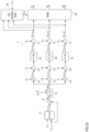
- Figure 1 shows a circuit diagram of a power converter 10 known as Vienna rectifier, which is a switched-mode three-phase (3 ⁇ ) AC-DC power converter.
- the power converter includes an input with three input nodes A, B, C each configured to receive a respective one of three input voltages V1, V2, V3, two DC link nodes X, Z configured to provide a DC link voltage V4 therebetween, and a midpoint Y coupled to each of the two DC link nodes X, Z.
- Each of the three input voltages V1, V2, V3 is a voltage between the respective input node A, B, C and a common ground node N.
- the power converter further includes three inductors L1, L2, L3 each coupled to a respective one of the three input nodes A, B, C.
- the inductors L1, L2, L3 are directly coupled to the inputs A, B, C. This, however is only an example. According to another example (not shown) an input filter is connected between the inputs A, B, C and the inductors L1, L2, L3.
- the power converter further includes a rectifier bridge 1 with three bridge legs 1 1 , 1 2 , 1 3 .
- Each of the three bridge legs 1 1 1 , 1 2 , 1 3 which are only schematically illustrated in Figure 1 , includes at least one electronic switch Q1, Q2, Q3 and is connected to a respective one of the three inductors L1, L2, L3, so that each of the bridge legs 11, 12, 13 is coupled to a respective one of the three inputs A, B, C through a respective one of the three inductors L1, L2, L3.
- each of the three bridge legs 1 1 , 1 2 , 1 3 is connected to the two DC link nodes X, Z and the midpoint Y.
- the midpoint Y may be coupled to a first one X of the two DC link nodes X, Z via a first capacitor C1 and to a second one Z of the two DC link nodes X, Z via a second capacitor C2.
- a voltage VC1 across the first capacitor C1 is referred to as first capacitor voltage and a voltage VC2 across the second capacitor C2 is referred to as second capacitor voltage in the following.
- the input voltages V1, V2, V3 received by the power converter are alternating input voltages such as sinusoidal input voltages.
- a phase shift between each pair of these input voltages V1, V2, V3 may be 120°.
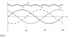
- Figure 2 shows signal diagrams of sinusoidal input voltages V1, V2, V3 during one period of each of these input voltages V1, V2, V3.
- a phase shift between each pair of these input voltages V1-V3 is 120° (2 ⁇ /3) in this example.
- Each of the three sinusoidal input voltages V1-V3 periodically changes between a minimum voltage level and a maximum voltage level, wherein the maximum voltage level is a positive voltage level and the minimum voltage level is a negative voltage level in this example.
- a magnitude of the minimum level essentially equals a magnitude of the maximum level and the three input voltages V1-V3 have essentially the same minimum voltage levels and the same maximum voltage levels. Further, the three input voltages V1-V3 may have essentially the same frequency, wherein this frequency is between 50 Hz and 60 Hz, for example.
- Figure 2 illustrates the input voltages V1, V2, V3 dependent on a phase angle.
- the plurality of the input voltages V1, V2, V3 is also referred to as input voltage system.
- a magnitude A1, A2, A3 of the maximum voltage level and the minimum voltage level of each of the input voltages V1, V2, V3 may also be referred to as amplitude of the respective input voltage V1, V2, V3.
- one of the three input voltages has the highest (positive) voltage level of the three input voltages V1, V2, V3 and one of the three input voltages has the lowest (negative) voltage level of the three input voltages V1, V2, V3, wherein in each period each of the three input voltages V1, V2, V3 has the highest level and each of the three input voltages V1, V2, V3 has the lowest level for a certain time period.
- a difference between the highest voltage level and the lowest voltage level is referred to as line-to-line voltage V LL .
- the line-to-line voltage V LL associated with the input voltages V1, V2, V3 shown in Figure 2 is also illustrated in Figure 2 .
- the line-to-line voltage is periodic, wherein the duration of one period of the line-to-line voltage V LL is 1/6 of a duration of one period of the input voltages V1, V2, V3.
- one period of the input voltages V1, V2, V3 includes phase angles from 0° to 360° (0 to 2 ⁇ ) and one period of the line-to-line voltage V LL ranges over 60° of one period of the input voltages V1, V2, V3.
- V LL_MAX A ⁇ 3 .
- Operating a power converter of the type shown in Figure 1 may include (a) regulating the DC link voltage V4 such that it has a predefined voltage level, and (b) regulating each of the three input currents I1, I2, I3 such that it has a current waveform that essentially equals the waveform of the respective input voltage V1, V2, V3.
- these input currents I1, I2, I3 essentially have sinusoidal waveforms when the input voltages V1, V2, V3 are sinusoidal voltages.
- Regulating each of the input currents I1, I2, I3 may include regulating an inductor voltage VL1, VL2, VL3 across the respective inductor L1, L2, L3, wherein regulating the inductor voltages VL, VL2, VL3 may include regulating voltages VA', VB', VC' at circuit nodes A', B', C' arranged between the inductors L1, L2, L3 and the bridge legs 1 1 , 1 2 , 1 3 .
- circuit nodes A', B', C' are referred to as switch nodes of the bridge legs 1 1 , 1 2 , 1 3 , and the voltages VA', VB', VC' at these switch nodes A', B', C', are referred to as switch node voltages in the following, wherein these voltages VA', VB', VC' are referenced to the common ground node N.
- switch node voltages in the following, wherein these voltages VA', VB', VC' are referenced to the common ground node N.
- Figure 3 illustrates a power converter of the type illustrated in Figure 1 , wherein the bridge legs 1 1 , 1 2 , 1 3 are implemented in accordance with one specific example. (Further examples for implementing the inductor voltages VL1, VL2, VL3 are explained herein further below.)
- Figure 4 illustrates signal diagrams of signals occurring in the power converter during one period of the input voltages V1, V2, V2.
- each of the bridge legs 1 1 1 , 1 2 , 1 3 includes an electronic switch Q1, Q2, Q3 connected between the respective switch node A', B', C' and the midpoint Y, a first rectifier element D11, D21, D31 connected between the respective input node A', B', C' and the first DC link node X, and a second rectifier element D12, D22, D32.
- the electronic switches Q1, Q2, Q3 may be implemented as bidirectional blocking switches.
- a "bidirectional blocking switch” is a switch that is capable of blocking a current independent of a polarity of a voltage applied to the electronic switch.
- the electronic switch Q (wherein Q represents an arbitrary one of switches Q1, Q2, Q3) includes two MOSFETs (Metal Oxide Semiconductor Field Effect Transistors) that are connected in series such that integrated body diodes are connected in a back-to-back configuration. That is, these MOSFETs are connected in series such that the body diodes integrated in these MOSFETs either have their anodes connected or have their cathodes connected.
- the two MOSFETs may be driven by the same drive signal S (wherein S represents an arbitrary one of the drive signals S1, S2, S3 received by the switches Q1, Q2, Q3).
- S represents an arbitrary one of the drive signals S1, S2, S3 received by the switches Q1, Q2, Q3
- the first and second rectifier elements D11-D32 may be implemented as passive rectifier elements such as diodes. This, however, is only an example. Active rectifier elements such as MOSFETs operated as synchronous rectifiers may be used as well.
- the first rectifier elements D11, D21, D31 are configured to enable a (positive) current flow from the respective switch node A', B', C' towards the first DC link node X and the second rectifier elements D12, D22, D32 are configured to enable a (positive) current flow from the second DC link node Z towards the respective switch node A', B', C'.
- the diodes forming the first rectifier elements D11, D21, D31 have their cathodes connected to the first DC link node X and have their anodes connected to the respective input node A', B', C'
- the diodes forming the second rectifier elements D12, D22, D32 have their anodes connected to the second DC link node Z and have their cathodes connected to the respective input node A', B', C'.
- controlling the current I1, I2, I3 through each of the inductors L1, L2, L3 includes controlling the voltage VL1, VL2, VL3 across the respective inductor L1, L2, L3.
- Each inductor voltage VL1, VL2, VL3 is given by the respective input voltage V1, V2, V3 minus the respective switch node voltage VA', VB', VC'.
- the input voltages V1, V2, V3 are predefined by a voltage source such as a power grid and can be measured, so that the inductor voltages VL1, VL2, VL3 and, therefore, the inductor currents I1, I2, I3 can be regulated by regulating the switch node voltages VA', VB', VC'. This is explained with reference to Figure 4 in the following.
- Figure 4 illustrates drive signals S1, S2, S3 of the electronic switches Q1, Q2, Q3, sinusoidal input voltages V1, V2, V3 and corresponding input currents I1, I2, I3, which are essentially sinusoidal.
- Figure 4 further illustrates currents ID11, ID12 through the first and second rectifier elements D 11, D 12 in a first one 1 1 of the bridge legs 1 1 , 1 2 , 1 3 , a current IQ1 through the electronic switch Q1 in the first bridge leg 1 1 , and a voltage VQ1 across the electronic switch Q1 in the first bridge leg 1 1 .
- the power converter is in a steady state in which the DC link voltage V4 has already reached a desired voltage level and that a power consumption of a load Z (illustrated in dashed lines in Figure 3 ) connected to the DC link nodes X, Z is constant.
- This load may be an arbitrary load, including a load that includes a further power converter.
- the power converter may be operated in a continuous conduction mode (CCM), that is, the inductor currents I1, I2, I3 do not decrease to zero during each of the positive and the negative halfwave of the respective input voltage V1, V2, V3. (The input currents I1, I2, I3 turn zero only for a short time period when the respective input voltage V1, V2, V3 crosses zero).
- CCM continuous conduction mode
- the "midpoint voltage” VY is the voltage at the midpoint Y, which is not directly connected to the ground node N, referenced to the ground node N.
- the midpoint voltage VY or the negative -VY of the midpoint voltage may also be referred to as common mode voltage VCM in the following.
- the common mode voltage VCM may be regulated such that it is zero, so that the potential at the midpoint equals the potential at the ground node.
- the common mode voltage VCM may be regulated such that it is different from zero and varies over one period of the input voltages V1, V2, V3.
- the inductor currents can be regulated such that each inductor current I1, I2, I3 is positive during the positive halfwave of the respective input voltage V1, V2, V3 and negative during the negative halfwave of the respective input voltage V1, V2, V3. Examples for regulating the common mode voltage VCM are explained in further detail herein below.
- Controlling the input currents I1, I2, I3 is explained in the following with reference to controlling the current I1 through a first one L1 of the inductors L1, L2, L3, which is the inductor connected to the first bridge leg 1 1 . Regulating the other two I2, I3 of the input currents I1, I2, I3 is achieved in the same way.
- first input the voltage V1 received at this input is referred to as first input voltage
- the switch node A' of the first bridge leg 1 1 is referred to as first switch node
- the inductor L1 connected to the first switch node A' is referred to as first inductor
- the voltage VL1 across the first inductor L1 is referred to as first inductor voltage VL1.
- the first inductor current I1 is positive, that is, the inductor current flows in a direction as indicated by the arrow in Figure 3 .
- the inductor current I1 flows through the first rectifier element D11 during the off-period of the first switch Q1, that is, after the first switch Q1 has been switched off.
- the voltage VA' at the first switch node A' is given by the voltage VX at the first DC link node X minus a voltage drop across the first rectifier element D11.
- This voltage drop across the first rectifier element is negligible so that during the off-period of the first electronic switch Q1, the potential at the first switch node A' is essentially clamped to the voltage VX at the first DC link node X.
- This voltage VX is referenced to the ground node and is referred to as first DC link node voltage in the following.
- the first inductor current I1 is negative, that is, the inductor current flows in a direction opposite the direction as indicated by the arrow in Figure 3 .
- the inductor current I1 flows through the second rectifier element D12 during the off-period of the first switch Q1.
- the potential at the first switch node A' is given by the voltage VZ at the second DC link node Z minus a voltage drop across the second rectifier element D12.
- This voltage drop across the second rectifier element is negligible so that during the off-period of the first electronic switch Q1, the potential at the first switch input node A' is essentially clamped to the voltage VZ at the second DC link node Z.
- This voltage VZ is referenced to the ground node and is referred to as second DC link node voltage in the following.
- the common mode voltage VCM can be positive and negative. In each case, the magnitude of the common mode voltage VCM is lower than the magnitude of each of the first and second capacitor voltages, so that the first DC link node voltage VX is positive and the second DC link node voltage VZ is negative.
- the inductor current I1 increases when the inductor voltage VL1 is positive, and decreases when the inductor voltage VL1 is negative, and remains constant when the inductor voltage VL1 is zero.
- the voltage VA' at the first switch node A' between two of these three voltage levels VX, VY, VZ the first input current I1 can be generated such that it follows a sinusoidal waveform.
- the inductor current I1 increases, when the average of the inductor voltage VL1 over one-period and one off-period of the first switch Q1 is positive and decreases when the average of the inductor voltage VL1 over one-period and one off-period of the first switch Q1 is negative.
- the electronic switch Q1 (as well as the other switches Q2, Q3) may be operated in a pulse-width modulated (PWM) fashion at a fixed switching frequency fsw, which is significantly higher than the frequency of the first input voltage V1.
- the switching frequency fsw is between several kHz and several 10 kHz and may range up to several 100 kHz, for example.
- of the duty cycle d1 is given by the ratio between the duration T OFF of the off-period and the duration T of the drive cycle,
- T OFF T .
- the duty cycle d1 can be positive or negative, wherein the duty cycle d1 is positive during the positive halfwave of the first input voltage V1 and negative during the negative halfwave of the first input voltage V1.
- a positive duty cycle d1 different from one (1) or zero (0) represents a ratio between the duration of the on-period and the off-period in a drive cycle in the positive halfwave of the first input voltage V1.
- a negative duty cycle d1 different from 1 or zero represents a ratio between the duration of the on-period and the off-period in a drive cycle in the negative halfwave of the first input voltage V1.
- the first switch node voltage VA' is obtained by switching between the first DC link node voltage VX and the midpoint voltage VY, or between the second DC link node voltage VZ and the midpoint voltage VY.
- the first switch node voltage A' is therefore given by the average voltage at the first switch node A' in one drive cycle.
- the duty cycle d1 of the first electronic switch Q1 the first switch node voltage VA' and, therefore, the first inductor voltage VL1 can be adjusted.
- the duty cycle d1 can be calculated.
- the duty cycle d1 is given by the ratio between the duration T OFF of the off-period and the duration T of one drive cycle, and the duty cycle d1 is positive in the positive halfwave of the first input voltage V1 and negative in the negative halfwave of the first input voltage V1.
- the power converter includes a control circuit 2 that is configured to operate the at least one electronic switch Q1, Q2, Q3 in each of the bridge legs 1 1 , 1 2 , 1 3 . More specifically, this control circuit 2 may be configured to generate drive signals S1, S2, S3 received by the electronic switches Q1, Q2, Q3 such that the DC link voltage V4 has a predefined voltage level and such that the inductor currents (the input currents) I1, I2, I3 essentially have the same waveform as the input voltages V1, V2, V3.
- the control circuit 2 receives a DC link voltage signal S V4 , wherein the DC link voltage signal S V4 represents the DC link voltage V4.
- the DC link voltage V4 may be measured in a conventional way by any kind of voltage measurement circuit (not shown) in order to obtain the DC link voltage signal S V4 .
- the control circuit 2 receives input voltage signals S V1 , S V2 , S V3 , each representing a respective one of the input voltages V1, V2, V3 and input current signals S I1 , S I2 , S I3 each representing a respective one of the input currents I1, I2, I3.
- the input voltage V1, V2, V3 may be measured in a conventional way in order to obtain the input voltage signals S V1 , S V2 , S V3 . Further, the input currents I1, I2, I3 may be measured in a conventional way in order to obtain the input current signals S I1 , S I2 , S I3 .
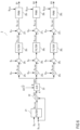
- One example of a control circuit 2 configured to generate the drive signals S1-S3 is illustrated in Figure 6 .
- the control circuit 2 shown in Figure 6 includes a first filter 21 that receives the DC link voltage signal S V4 and a DC link voltage reference signal S V4_REF , wherein the DC link voltage reference signal S V4_REF represents the desired voltage level of the DC link voltage V4.
- the filter 21 subtracts the DC link voltage reference signal S V4_REF from the DC link voltage signal S V4 and filters the difference in order to generate a DC link voltage error signal S V4_ERR .
- the filter (or controller) may have one of a proportional (P) characteristic, a proportional-integrative (PI) characteristic, a proportional-integrative-derivative (PID) characteristic, or the like.
- a multiplier 22 receives the DC link voltage error signal S V4_ERR and the DC link voltage reference signal S V4_REF , wherein an output signal S22 of the multiplier 22 represents a desired output power of the power converter.
- a divider 23 divides the multiplier output signal S22 by a signal that represents 1.5 times the square of the amplitude of the input voltages V1, V2, V3 3 2 ⁇ V ⁇ 2 .
- An output signal S23 of the divider 23 represents an overall desired input current of the power converter, wherein the overall desired input current is the input current that is required by the power converter in order to achieve the desired voltage level of the DC link voltage V4 as defined by the DC link voltage reference signal S V4_REF .
- the control circuit 2 further includes three branches, wherein each of these branches receives the divider output signal S23 and generates a respective one of the three drive signals S1, S2, S3.
- Each of these branches includes a multiplier 24i, 24 2 , 24 3 that multiplies the divider output signal S23 with the respective input voltage signal S V1 , S V2 , S V3 , wherein an output signal of each of these multipliers 24 1 , 24 2 , 24 3 is an input current reference signal S I1_REF , S I2_REF , S I3_REF , that is, each of these signals S I1_REF , S I2_REF , S I ⁇ _REF represents the desired current level of a respective one of the input currents I1, I2, I3.
- each of these subtractors 25 1 , 25 2 , 25 3 is filtered by a respective filter 26 1 , 26 2 , 26 3 connected downstream the respective subtractor 25 1 , 25 2 , 25 3 , wherein an output signal S VL1_REF , S VL2_REF , S VL3_REF of the respective filter 26 1 , 26 2 , 26 3 represents a desired voltage level of a respective one of the three inductor voltages VL1, VL2, VL3.
- a further subtractor 27 1 , 27 2 , 27 3 subtracts the input voltage signal S V1 , S V2 , S V3 from the respective inductor voltage reference signal S VL1_REF , S VL2_REF , S VL3_REF in order to obtain switch node voltage reference signals S VA'_REF , S VB'_REF , S VC'_REF , wherein each of these switch node voltage reference signals S VA'_REF , S VB'_REF , S VC'_REF represents the desired voltage level of a respective one of the three leg input voltages VA', VB', VC'.
- each of the three branches that generate the drive signals S1, S2, S3 includes a PWM modulator 28 1 , 28 2 , 28 3 that receives a respective one of the leg input voltage reference signals S VA'_REF , S VB'_REF , S VC'_REF , wherein each of these modulators 28 1 , 28 2 , 28 3 is configured to generate a respective one of the drive signals S1, S2, S3 based on the respective reference signal S VA'_REF' , S VB'_REF , S VC'_REF such that in each drive cycle of the at least one electronic switch Q1, Q2, Q3 an average of the respective leg input voltage VA', VB', VC' equals the voltage level as defined by the respective leg input voltage reference signal S VA'_REF' , S VB'_REF' , S VC'_REF .
- the specific implementation of the PWM modulators 28 1 , 28 2 , 28 3 is dependent on the type of a bridge
- each of the PWM modulators 28 1 , 28 2 , 28 3 may be configured to calculate the duty cycles d1, d2, d3 of the drive signals S1, S2, S3 based on one of equations (3a), (3b) or (3c) and generate the drive signals S1, S2, S3 in accordance with the calculated duty cycle.
- the duty cycles d1, d2, d3 not only the switch node voltages VA', VB', VC' but also the common mode voltage VCM can be adjusted.
- the first DC link node voltage VX has to be equal to or higher than the highest voltage level of the three input voltages V1, V2, V3 and the second DC link node voltage VZ has to be equal to or lower than the lowest voltage level of the three input voltages V1, V2, V3.
- the common mode voltage VCM is zero
- each of the capacitor voltages VC1, VC2 has to be higher than the amplitude of the three input voltages.
- the switch node voltages VA', VB', BC' follow the input voltages V1, V2, V3 and can be considered to be essentially equal to the input voltages V1, V2, V3 (the inductor voltages VL1, VL2, VL3 are low as compared to the input voltages V1, V2, V3).
- the PWM modulators 28i, 28 2 , 28 3 may each receive a common mode voltage signal S VCM that represents the desired common mode voltage.
- This common mode signal S VCM may be provided by a central controller (which is not illustrated). This central controller may be a microcontroller or the like.
- the electronic switch Q1, Q2, Q3 in each of the bridge legs 11, 12, 13 is operated in the PWM mode throughout the period of the input voltages V1, V2, V3.
- This type of operating mode will also be referred to as 3/3 mode in the following.
- the bridge legs 1 1 1 , 1 2 , 1 3 can be implemented in various ways. Some examples for implementing the individual bridge legs 1 1 -1 3 are explained with reference to the first bridge leg 1 1 in the following.
- the second and third bridge leg 1 2 . 1 3 can be implemented in the same way as the first bridge leg 1 1 .
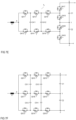
- Figure 7A illustrates a first example of the first bridge leg 1 1- In this example, the first bridge leg 1 1 is implemented in the way explained with reference to Figure 3 .
- the bridge leg 1 1 includes a bidirectional blocking switch Q1 connected between the first switch node A' and the midpoint Y, a first rectifier element D11 connected between the first switch node A' and the first DC link node X, and a second rectifier element D12 connected between the second DC link node Z and the first switch node A'.
- the bridge leg 1 1 includes a first rectifier element D211 connected to the first DC link node X, a second rectifier element D212 connected to the second DC link node Z, a third rectifier element D213 connected between the switch node A' and the first rectifier element D211, a fourth rectifier element D214 connected between the switch node A' and the second rectifier element D212, a fifth rectifier element D215 connected between the midpoint Y and the first rectifier element D211, and a sixth rectifier element D216 connected between the midpoint Y and the second rectifier element D212.
- an electronic switch Q1 is connected between the first and second rectifier elements D211, D212.
- This electronic switch Q1 may be a unidirectional electronic switch such as, for example, a MOSFET.
- the rectifier elements D211-D216 may be implemented as diodes. These rectifier elements D211-D216 are connected such that during the positive halfwave of the first input voltage V1, the inductor current I1 can flow from the first switch node A' via the third rectifier element D213, the electronic switch Q1 and the sixth rectifier element D216 to the midpoint Y, when the electronic switch Q1 is switched on. When the electronic switch Q1 is switched off, the inductor current I1 flows via the third rectifier element D213 and the first rectifier element D211.
- the current flows from the midpoint Y via the fifth rectifier element D215 and the fourth rectifier element D214 to the first switch node A' when the electronic switch Q1 is switched on.
- the current flows from the second DC link node Z via the second rectifier element D212 and the fourth rectifier element D214 to the first switch node A'.
- Figure 7C shows a third example of the first bridge leg 1 1 .
- the first bridge leg 1 1 includes a first rectifier element D311 connected to the first DC link node X, a second rectifier element D312 connected to the second DC link node Z, a first switch Q311 connected between the first switch node A' and the first rectifier element D311, a second switch Q312 connected between the first switch node A' and the second rectifier element D312, a third rectifier element D313 connected between the midpoint Y and the first rectifier element D311, and a fourth rectifier element D314 connected between the midpoint Y and the second rectifier element D312.
- the electronic switches Q311, Q312 may be unidirectional blocking switches such as, for example, MOSFETs.
- the electronic switches Q311, Q312 and the rectifier elements D311-D314 may be connected such that during the positive halfwave of the input voltage V1 the inductor current I1 flows via the switch node A' via the second electronic switch Q312 and the fourth rectifier element D314 to the midpoint Y when the second electronic switch Q312 is switched on.
- the second electronic switch Q312 is switched off, the inductor current I1 flows via the first electronic switch Q311 and the first rectifier element D311 to the first DC link node X.
- the first electronic switch Q311, Q312 may be switched on and off at the same time.
- the inductor current I1 flows via the body diode of the MOSFET forming the first electronic switch Q311 and the first rectifier element D311.
- the first and second electronic switch Q311, Q312 are operated in a complementary fashion, so that only one of the switches is switched on at the same time.
- the first switch Q311 is switched on when the second switch Q312 switches off, so that the inductor current I1 flows via the switched on first electronic switch Q311 and the first rectifier element D311.
- the inductor current I1 flows from the midpoint Y via the third rectifier element D311 and the first electronic switch Q311 to the first switch node A' when the first electronic switch Q311 is switched on.
- the inductor current I1 flows from the second DC link node Z via the second rectifier element D311 and the second electronic switch Q312 to the first switch node A'.
- Figure 7D shows a modification of the bridge leg 11 shown in Figure 7C .
- the first switch Q311 is connected between the midpoint Y and the first rectifier element D311
- the second switch Q312 is connected between the midpoint Y and the second rectifier element D312
- the third rectifier element D313 is connected between the switch node A' and the first rectifier element D311
- the fourth rectifier element D314 is connected between the switch node A' and the second rectifier element D311.
- Each of the bridge legs 1 1 shown in Figures 7A, 7B , 7C and 7D is configured to provide three different voltage levels at the first switch node A'.
- the average electrical potential at the first switch node A' during one drive cycle is generated from two voltage levels, the electrical potential VX at the first DC link node X and the electrical potential VY at the midpoint Y during the positive halfwave at the input voltage V1, and the electrical potential VZ at the second DC link node Z and the electrical potential VY at the midpoint Y during the negative halfwave of the input voltage V1.
- FIGS 7E and 7F illustrate further examples of the first bridge leg 1 1 .
- the bridge leg 1 1 includes capacitors in addition to DC link capacitors C1, C2.
- the bridge legs 1 1 illustrated in Figures 7D and 7E are so-called multi-level bridge legs, wherein the bridge leg 1 1 shown in Figure 7D is a Hybrid Active Neutral Point Clamped Converter leg, and the bridge leg 1 1 shown in Figure 7E is a Stacked Multicell Converter leg. These legs are known (see, for example, G. Gateau, T.A. Meynard, H.
- each of these bridge legs is capable of providing more than three different voltage levels, that is, the three voltage levels VX, VY, VZ and additional voltage levels for generating the switch node voltage VA'.
- the rectifier elements may be implemented as diodes (as illustrated). This, however, is only an example. According to another example (not shown) these rectifier elements may be implemented as synchronous rectifier elements.
- operating a power converter of the type illustrated in Figures 1 and 3 may include a PWM (pulse-width modulated) operation of each of the at least one electronic switch in each of the bridge legs 1 1 , 1 2 , 1 3 at each time of the operation.
- PWM pulse-width modulated
- Operating the switches Q1, Q2, Q3 in a PWM mode is associated with switching losses.
- Switchching losses are losses that occur in context with switching on and switching off the respective switch Q1, Q2, Q3. In order to increase the efficiency of the power converter it is desirable to reduce those switching losses.
- reducing switches losses includes operating the power converter in a reduced switching mode, wherein operating the power converter in a reduced switching mode includes deactivating the at least one switch Q1, Q2, Q3 in one or two of the bridge legs 1 1 , 1 2 , 1 3 for a time period that is significantly longer than the duration T of one drive cycle.
- deactivating the at least one switch includes deactivating the at least one switch for more than 10, more than 100 or even more than 1000 drive cycles.
- a bridge leg in which the at least one switch is deactivated is referred to as deactivated bridge leg.
- the "at least one electronic switch" of a bridge leg 1 1 , 1 2 , 1 3 may include one electronic switch or several electronic switches.
- a bridge leg 1 1 with one electronic switch is illustrated in Figure 7A wherein, as illustrated in Figure 5 , one switch may include two transistors.
- Bridge legs 1 1 with several (unidirectional blocking) switches are illustrated in Figures 7B-7F .
- “deactivating the at least one switch” includes deactivating each of the several switches.
- “the at least one electronic switch” is a switch that is used in a respective bridge leg to connect the switch node to the midpoint Y or to a circuit node having a voltage between the voltage at the midpoint Y and one of the first and second DC link node voltages VX, VZ.
- Voltages between the voltage at the midpoint Y and one of the first and second DC link node voltages VX, VZ are provided in the bridge legs illustrated in Figures 7E and 7F , for example.
- the rectifier elements that couple the switch nodes A', B', C' to the first and second DC link nodes X, Z may include an electronic switch.
- "deactivating the at least one switch” does not include deactivating electronic switches acting as (synchronous) rectifiers.
- Figure 8 illustrates signal diagrams of the drive signals S1, S2, S3, the input voltages V1, V2, V3, the DC link voltage V4, the input currents I1, I2, I3, the currents ID11, ID12, IQ11 in the first bridge leg 1 1 and the voltage VQ1 across the first switch Q1 in the first bridge leg 1 1 .
- the operating mode illustrated in Figure 8 is referred to as 1/3 mode in the following.
- a bridge leg in which the at least one electronic switch is operated in the PWM mode is referred to as "activated bridge leg”
- a bridge leg in which the at least one electronic switch is deactivated is referred to as “deactivated bridge leg” although a current may of course flow in the deactivated bridge leg between the respective switch node and one of the first and second DC link nodes X, Z.
- the power converter is operated in the 1/3 mode throughout the period of the input voltages V1, V2, V3. That is, at each time of the period of the input voltages V1, V2, V3 only one of the bridge legs 1 1 , 1 2 , 1 3 is activated and the other two bridge legs are deactivated.
- This type of operating mode is referred to as full 1/3 mode in the following. This, however, is only an example. According to another example explained further below it is also possible to operate the power converter such that only in some time periods (at some phase angles of one period of the input voltages V1, V2, V3) it operates in the 1/3 mode.
- the switch node voltage of a deactivated bridge leg is either clamped to the DC link voltage VX at the first DC link node X or the DC link voltage VZ at the second DC node Z.
- the switch node voltage of one bridge leg is clamped to the first DC link node voltage VX, and the switch node voltage of another bridge leg is clamped to the second DC link node voltage VZ.
- the bridge legs that are deactivated change over one period of the input voltage system. This is explained with reference to signal diagrams illustrated in Figure 13 herein further below..
- the currents through the two inductors that are connected to the deactivated bridge legs are regulated by suitably regulating the DC link voltage V4 by a further power converter 5 connected to the DC link nodes X, Z of the power converter.
- a power converter arrangement with a power converter of the type explained before and a further power converter 5 connected to the DC link nodes X, Z of the power converter is illustrated in Figure 10 .
- the power converter 10 is also referred to as first power converter and the further power converter 5 is also referred to as second power converter in the following.
- the second power converter 5 may be configured to provide a constant output current I OUT or a constant output voltage V OUT different from the DC link voltage V4.
- the second power converter 5 contributes to the regulation of the inductor currents I1, I2, I3 in the first power converter 10 by suitably regulating the DC link voltage V4 there is no increase of the losses occurring in the second power converter 5.
- the switching losses in the first power converter are significantly reduced. Thus, there is a synergy between the control of the first power converter and the control of the second power converter 5.
- control circuit 4 configured to operate a power converter arrangement with a first power converter and a second power converter of the type shown in Figure 9 is illustrated in Figure 10 .
- the control circuit 4 shown in Figure 10 includes two main branches (or subcircuits), a first branch 40 configured to operate the first power converter and a second branch 6 configured to operate the second power converter 5.
- the block diagram shown in Figure 10 illustrates the functional blocks of the control circuit 4 rather than a specific implementation. Those functional blocks can be implemented in various ways. According to one example, these functional blocks are implemented using dedicated circuitry. According to another example, the control circuit 4 is implemented using hardware and software.
- the first control circuit includes a microcontroller and software executed by the microcontroller.
- the output current I OUT of the second power converter 5 is regulated and that the output voltage V OUT is defined by a load (not shown) receiving the output current.
- the load may be a battery that receives the output current I OUT and defines the output voltage V OUT .
- the first branch 40 of the control circuit 4 shown in Figure 10 is based on the control circuit shown in Figure 6 , wherein the same elements have the same reference characters.
- the control circuit 4 receives an output current signal S IOUT wherein the output current signal S IOUT represents the output current I OUT .
- the output current I OUT may be measured in a conventional way by any kind of current measurement circuit (not shown) in order to obtain the output current signal S IOUT .
- the control circuit 4 includes a first filter 41 that receives the output current signal S IOUT and an output current reference signal S IOUT_REF , wherein the an output current reference signal S IOUT REF represents the desired current level of the output current I OUT .
- the first filter 41 subtracts the output current reference signal S IOUT REF from the output current signal S IOUT , for example, and filters the difference in order to generate an output signal S V51_REF .
- this output signal S V51_REF represents a desired voltage V51 across an inductor 51 in the second power converter 5, wherein this inductor 51 carries the output current I OUT .
- FIG. 9 One example of such inductor 51 is illustrated in Figure 9 .
- the filter may have one of a proportional (P) characteristic, a proportional-integrative (PI) characteristic, a proportional-integrative-derivative (PID) characteristic, or the like.
- a adder 42 receives the filter output signal S V51_REF and an output voltage signal S VOUT that represents the output voltage V OUT , wherein an output signal S42 of the adder 42 and the filter output signal S V51_REF are received by a multiplier.
- An output signal S43 of the multiplier 43 represents a desired output power of the power converter arrangement.
- the divider 23 already explained with Figure 6 divides the multiplier output signal S43 by a signal that represents 1.5 times the square of the amplitude of the input voltages V1, V2, V3 ( 3 2 ⁇ V ⁇ 2 ).
- An output signal S23 of the divider 23 represents an overall desired input current of the first power converter.
- the divider output signal S23 is processed by the three branches explained with reference to Figure 6 before in order to generate the three switch node voltage reference signals S VA'_REF , S VB'_REF , S VC'_REF .
- the current control loop is the slowest one of the control loops explained in context with Figure 10 .
- Controlling the output current I OUT by the control circuit 4 is only an example.
- the output voltage V OUT is controlled.
- the filter 41 receives the output voltage signal S VOUT and an output voltage reference signal S VOUT_REF representing the desired voltage level of the output voltage V OUT .
- the adder 42 is omitted and the multiplier 43 receives the output signal from the filter 41 and the output voltage reference signal S VOUT_REF .
- a PWM modulator 44 receives the switch node voltage reference signals S VA'_REF , S VB'_REF , S VC'_REF . From these switch node voltage reference signals S VA'_REF , S VB'_REF , S VC'_REF the PWM modulator 44 (a) selects a maximum and deactivates the bridge leg associated with the maximum voltage reference signal; (b) selects a minimum and deactivates the bridge leg associated with the minimum voltage reference signal; and (c) operates the remaining bridge leg in the PWM mode.
- the "remaining bridge leg" is the bridge leg, associated with the switch node reference signal that is between the maximum and the minimum switch node voltage reference signal. This switch node voltage reference signal is referred to as intermediate switch node voltage reference signal in the following.
- the second branch 6 of the control circuit also receives the three switch node voltage reference signals S VA'_REF , S VB'_REF , S VC'_REF and is configured to control operation of the second power converter 5 based on these signals S VA'_REF , S VB'_REF , S VC'_REF .
- S VA'_REF switch node voltage reference signals
- S VB'_REF switch node voltage reference signals
- Figure 11 illustrates one example of the second power converter 5.
- the second power converter 5 includes a first converter stage 51 and a second converter stage 52, wherein each of these a first and second converter stages 51, 52 includes a first input node 511, 521, a second input node 512, 522, a first output node 513, 523, and a second output node 514, 524.
- the first input node 511 of the first converter stage 51 may be connected to the first DC link node X
- the second input node 522 of the second converter stage 52 may be connected to the second DC link node Z
- the second input node 512 of the first converter stage 51 and the first input node 521 of the second converter stage 52 may be connected with each other and connected to the midpoint Y.
- the second output node 514 of the first converter stage 51 and the first output node 523 of the second converter stage 52 may be connected with each other.
- the output voltage V OUT is the voltage between the first output node 513 of the first converter stage 51 and the second output node 524 of the second converter stage 52.
- the converter stages 51, 52 may each be implemented with one of various different converter topologies.
- each of the converter stages 51, 52 is implemented as an isolated DC-DC converter, that is, a DC-DC converter that includes a transformer between the respective input 511, 512 or 521, 522 and the respective output 513, 514 or 523, 534.
- each of the converter stages 51, 52 is implemented as a non-isolated DC-DC converter, that is, a DC-DC converter that does not include a transformer between the respective input 511, 512 or 521, 522 and the respective output 513, 514 or 523, 534.
- Examples of different types of DC-DC converters that are suitable to be used as first and second converter stage 51, 52 include, but are not restricted to: a flyback converter (isolating), an LLC converter (isolating), dual active bridge (DAB) converter (isolating), a phase-shifted full bridge converter (isolating), a buck-boost converter, a boost-buck converter, etc.
- a flyback converter Isolating
- an LLC converter Isolating
- DAB dual active bridge
- phase-shifted full bridge converter isolating
- buck-boost converter a boost-buck converter
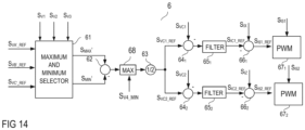
- This control circuit 6 includes a maximum and minimum selector 61 that receives the three switch node voltage reference signals S VA'_REF , S VB'_REF , S VC'_REF .
- the first signal S MAX ' is also referred to as maximum switch node voltage reference signal S MAX ', and the second signal S MIN ' is also referred to as minimum switch node voltage reference signal.
- the intermediate switch node voltage reference signal is also referred to as S INT ' in the following.
- the second control circuit branch 6 is configured to operate the second power converter 5 in such a way that the DC link voltage V4 equals a voltage that is represented by the difference between the maximum switch node voltage reference signal S MAX ' and the minimum switch node voltage reference signal S MIN '. Referring to the above, the switch nodes of the bridge legs that are deactivated are clamped to the first DC link node voltage VX and the second DC link node voltage VZ, respectively.
- the switch nodes that are clamped to the first and second DC link nodes X, Z receive the switch node voltages calculated by the first control circuit branch 40.
- the inductor currents of those inductors connected to deactivated bridge legs have a current level as represented by the respective input current reference signal calculated by the first control circuit branch 40.
- the second control circuit branch 6 includes a subtractor 62 that subtracts the minimum switch node voltage reference signal S MIN from the maximum switch node voltage reference signal S MAX ', wherein a multiplier 63 multiplies an output signal of the subtractor with 0.5.
- An output signal of the multiplier forms a first capacitor voltage reference signal S VC1_REF and a second capacitor voltage reference signal S VC2_REF , wherein the first capacitor voltage reference signal S VC1_REF represents a desired value of the first capacitor voltage VC1, and the second capacitor voltage reference signal S VC2_REF represents a desired value of the second capacitor voltage VC2.
- the second control circuit branch 6 includes a first branch and a second branch.
- the first branch receives the first capacitor voltage reference signal S VC1_REF and is configured to provide a first input current reference signal S I51_REF , wherein the first input current reference signal S I51_REF represents a desired input current I51 of the first converter stage 51.
- the second branch receives the second capacitor voltage reference signal S VC2_REF and is configured to provide a second input current reference signal S I52_REF , wherein the second input current reference signal S I52_REF represents a desired input current I52 of the second converter stage 52.
- the first branch includes a subtractor 64 1 that subtracts a first capacitor voltage signal S CV1 , which represents the first capacitor voltage VC1, from the first capacitor voltage reference signal S VC1_REF .
- An output signal of the subtractor is filtered by a filter 65 1 , wherein an output signal S IC1_REF of the filter represents a desired current level of a current into the first capacitor C1.
- the first input current reference signal S I51_REF is given by a difference between a current signal Six that represents a current into the first DC link node X (wherein this current IX is provided by the first power converter) and the filter output signal S IC1_REF .
- the second branch includes a subtractor 64 2 that subtracts a second capacitor voltage signal S CV2 , which represents the second capacitor voltage VC2, from the second capacitor voltage reference signal S VC2_REF .
- An output signal of the subtractor is filtered by a filter 65 2 , wherein an output signal S IC2_REF of the filter represents a desired current level of a current into the second capacitor C2.
- the second input current reference signal S I52_REF is given by a difference between a current signal S IZ that represents a current into the second DC link node Z (wherein this current IZ is provided by the first power converter) and the filter output signal S IC2_REF .
- a first PWM modulator 67 1 receives the first input current reference signal S I51_REF and a first input current signal S I51 , wherein the latter represents the first input current 151, and is configured to control operation of one or more switches (not shown in the figures) included in the first converter stage 51 such that the first input current I51 has a current level as represented by the first input current reference signal S I51_REF .
- a second PWM modulator 67i receives the second input current reference signal S I52_REF and a second input current signal S I52 , wherein the latter represents the second input current I52, and is configured to control operation of one or more switches (not shown in the figures) included in the second converter stage 52 (not shown in the figures) such that the first input current 151 has a current level as represented by the first input current reference signal S I51_REF .
- the specific implementation of the PWM modulators 67 1 , 67 2 is dependent on the specific type of power converter used to implement the first and second converter stages 51, 52. However, PWM modulators configured to control the input current in various kinds of DC-DC converters are known, so that no further explanations are required in this regard.
- activating one of the three bridge legs 1 1 , 1 2 , 1 3 and deactivating the two other bridge legs 1 1 , 1 2 , 1 3 by the PWM modulator 44 in the 1/3 mode is dependent on the switch node voltage reference signals S VA'_REF , S VB'_REF , S VC'_REF .
- Time instances at which two of these switch node voltage reference signals S VA'_REF , S VB'_REF , S VC'_REF are equal can be neglected, so that at each time, from these switch node voltage reference signals S VA'_REF , S VB'_REF , S VC'_REF , one forms the maximum switch node voltage reference signal S MAX ', one forms the intermediate switch node voltage reference signal S INT ', and one forms the minimum switch node voltage reference signal S MIN '. This is explained with reference to Figure 13 in greater detail.
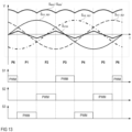
- Figure 13 illustrates signal diagrams of switch node voltage reference signals S VA'_REF , S VB'_REF , S VC'_REF , wherein each of these signals represents the desired voltage value of the respective switch node voltage VA', VB', VC'.
- Figure 13 further illustrates which of the bridge legs is operated in the PWM mode at which time or phase angle. Referring to the above and as illustrated in Figure 13 , in the steady state, each of the switch node voltage reference signals S VA'_REF , S VB'_REF , S VC'_REF follows the respective input voltage.
- a relationship between the individual switch node voltage reference signals S VA'_REF , S VB'_REF , S VC'_REF changes several times within one period.
- the "relationship" means the signal level of one of the switch node voltage reference signals S VA'_REF , S VB'_REF , S VC'_REF relative to the signal levels of the other two of the switch node voltage reference signals S VA'_REF , S VB'_REF , S VC'_REF .
- time periods P1-P6 which are also referred to as operating phases in the following, wherein in each of these time periods P1-P6 the relationship between the switch node voltage reference signals S VA'_REF , S VB'_REF , S VC'_REF does not change.
- the signal levels of the switch node voltage reference signals S VA'_REF , S VB'_REF , S VC'_REF vary in the individual operating phases P1-P6.
- the first switch node voltage reference signal S VA'_REF has the highest voltage level. That is, the voltage level of the first switch node voltage reference signal S VA'_REF is higher than the voltage level of a second one S VB'_REF of the switch node voltage reference signals S VA'_REF , S VB'_REF , S VC'_REF and the signal level of a third one S VC'_REF of the switch node voltage reference signals S VA'_REF , S VB'_REF , S VC'_REF . Further, in the first operating phase P1, the second switch node voltage reference signal S VB'_REF V2 hast the lowest voltage level.
- the voltage level of the second switch node voltage reference signal S VB'_REF is lower than the signal level of the first switch node voltage reference signal S VA'_REF and the signal level of the third switch node voltage reference signal S VC'_REF .
- the third switch node voltage reference signals S VA'_REF , S VB'_REF , S VC'_REF has a signal level between the voltage level of the first switch node voltage reference signal S VA'_REF and the signal level of the second switch node voltage reference signal S VB'_REF .
- the first switch node voltage reference signal S VA'_REF is the maximum switch node voltage reference signal S MAX '
- the second switch node voltage reference signal S VB'_REF is the minimum switch node voltage reference signal S MIN '
- the third switch node voltage reference signal S VC'_REF is the intermediate switch node voltage reference signal S INT ' _REF .
- the first switch node voltage reference signal S VA'_REF is the maximum switch node voltage reference signal S MAX '
- the second switch node voltage reference signal S VB'_REF is the intermediate switch node voltage reference signal S INT '
- the third switch node voltage reference signal S VC'_REF is the minimum switch node voltage reference signal S MIN ' REF .
- the input voltage having the highest voltage level is referred to as maximum input voltage Vmax
- the input voltage having the lowest voltage level is referred to as minimum input voltage Vmin
- the input voltage having a voltage level between the highest voltage level and the lowest voltage level is referred to as intermediate input voltage V INT .
- the switch node voltage reference signals S VA'_REF , S VB'_REF , S VC'_REF in the steady state, essentially follow the input voltages V1, V2, V3, so that the output signal S MAX '- S MIN ' of the subtractor 62 shown in Figure 12 essentially represents the line-to-line voltage V LL .
- the subtractor output signal S MAX '- S MIN ' is also illustrated in Figure 13 .
- operating the power converter in the 1/3 mode includes activating the bridge leg associated with the intermediate voltage reference signal S INT ' and deactivating the bridge legs associated with the maximum switch node voltage reference signal S MAX ' and the minimum switch node voltage reference signal S MIN '. That is, in the first operating phase P1, for example, the third bridge leg 1 3 is activated, in the second operating phase P2 the second bridge leg 1 2 is activated, and so on.
- the bridge legs 1 1 1 , 1 2 , 1 3 are activated and deactivated by the PWM modulator 44 in the control circuit 4.
- a common mode voltage signal S VCM representing this common mode voltage V CM is also illustrated in Figure 13 over one period of the input voltages.
- dmax denotes the duty cycle of the bridge leg associated with the maximum switch node voltage reference signal S MAX ' in a respective operating phase
- dmin denotes the duty cycle of the bridge leg associated with the minimum switch node voltage reference signal S MIN ' in a respective operating phase
- Vmax' denotes the desired switch node voltage represented by the maximum switch node voltage reference signal S MAX '
- Vmin' denotes the desired switch node voltage represented by the minimum switch node voltage reference signal S MIN '.
- the DC link voltage V4 is adjusted by the second converter 5 such that it equals Vmax'-Vmin', wherein Vmax' is the maximum of the desired switch node voltages and Vmin' is the minimum of the desired switch node voltages.
- Vmax' is the maximum of the desired switch node voltages
- Vmin' is the minimum of the desired switch node voltages.
- these desired switch node voltages Vmax', Vmin' essentially equal the maximum input voltage Vmax and the minimum input voltage Vmin, respectively, so that the varying DC link voltage V4 essentially equals the line-to-line voltage V LL .
- This is the lowest possible DC link voltage at which sinusoidal input currents I1, I2, I3 can be achieved, wherein the common mode voltage V CM is different from zero and given by equation (5) in this case.
- the power converter arrangement illustrated in Figure 9 is not restricted to generate the DC link voltage V4 such that it is defined by S MAX '-S MIN ' and essentially equals the line-to-line voltage V LL .
- a maximum selector 68 receives the subtractor output signal S62 and a minimum DC link voltage signal S V4_MIN , wherein the minimum DC link voltage signal S V4_MIN represents the minimum of the DC link voltage V4 that should be generated at the output of the first power converter 10.
- the maximum selector outputs the maximum of the two signal it receives to the multiplier 63.
- the voltage represented by the minimum DC link voltage signal S V4_MIN is referred to as minimum desired DC link voltage V4 MIN in the following.
- the DC link voltage V4 is generated such that it is generated based on the subtractor output signal S62 in time periods in which the subtractor output signal S62 is higher than the minimum desired DC link voltage signal S V4_MIN . In the remainder of the time the DC link voltage V4 is generated based on the minimum desired DC link voltage signal S V4_MIN .
- the power converter is not operated in the 1/3 mode throughout each of the six operating phases anymore. Instead there are time periods in which the first power converter is operated in the 1/3 mode, but also time periods in which each of the bridge legs 1 1 , 1 2 , 1 3 operate in the PWM mode. This is illustrated between a second time instance t2 and a third time instance t3 in Figure 15 .
- the minimum desired DC link voltage V4 MIN is the minimum of the DC link voltage V4, which is also illustrated in Figure 15 .
- the duration in which the power converter operates in the 1/3 mode during one period of the input voltages V1, V2, V3 decreases as the minimum DC link voltage V4 MIN increases.
- the operating mode in which the power converter alternatingly operates in the 1/3 mode and the 3/3 mode is referred to as partial-boost mode in the following.
- the power converter When calculating the duty cycles d1, d2, d3 in accordance with equations (4a)-(4c), the power converter automatically changes between the 1/3 mode and the 3/3, because these duty cycles are dependent on the DC link voltage V4 that is adjusted by the second power converter 5.
- the common mode voltage V CM In the partial-boost mode, the common mode voltage V CM may be the same as in the full 1/3 mode. However, in those time periods in which the power converter, in the partial-boost mode, operates in the 3/3 mode the common mode voltage V CM may be different from the common mode voltage in the 1/3 mode. Only in the full 1/3 mode, the common mode voltage VCM is constrained to the value presented in equation (5).
- the degree of freedom that is available to adjust the common mode voltage VCM may be used to adjust the common mode voltage VCM such that a current IY into the midpoint is minimized. This is explained in detail herein further below.
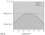
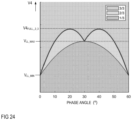
- Figure 16 illustrates the different operating modes of the first power converter 10 dependent on the minimum desired DC link voltage signal S V4_MIN and the phase angle of the input voltages V1, V2, V3. More specifically, Figure 16 illustrates the different operating modes in an arbitrary one of the six operating phases P1-P6, wherein each of these operating phases covers 60° of one period of the input voltages V1, V2, V3.
- a phase angle of 0° represents the beginning of the respective operating phase
- a phase angle of 60° represents the end of the respective operating phase
- a phase angle of 30° represents the middle of the respective operating phase, which is when the intermediate input voltage in the respective operating phase crosses zero.
- the power converter operates in the full 1/3 mode when the minimum desired DC link voltage signal S V4_MIN is below a minimum of the subtractor output signal S62.
- the subtractor output signal S62 essentially represents the line-to-line voltage V LL , so that the power converter operates in the full 1/3 mode when the minimum desired DC link voltage V4 MIN is below the minimum line-to-line voltage V LL_MIN .
- the power converter operates in the partial-boost mode when the minimum desired DC link voltage signal S V4_MIN is between the minimum of the subtractor output signal S62 and a maximum of the subtractor output signal S62.
- the maximum of the subtractor output signal S62 essentially equals the maximum line-to-line voltage V LL_MAX , so that the power converter operates in the in the partial-boost mode when the DC link voltage V4 is between the minimum line-to-line voltage V LL_MIN and the maximum line-to-line voltage V LL_MAX .
- the portion of the operating phase in which the power converter operates in the 3/3 mode increases as the minimum desired DC link voltage V4 MIN increases and the portion of the operating phase in which the power converter operates in the 1/3 mode decreases as the minimum desired DC link voltage V4 MIN increases.
- the power converter operates in the full 3/3 mode when the minimum desired DC link voltage signal S V4_MIN is higher than the maximum of the subtractor output signal S62.
- the DC link voltage V4 is essentially constant and only dependent on the minimum desired DC link voltage signal S V4_MIN .
- the duty cycles d1, d2, d3 may be calculated based on equations (3a) and (3b) by the PWM modulator 44 in the control circuit 4.
- the second control circuit branch 6 may include a maximum selector of the type explained with reference to Figure 14 .
- the first and second converter stages 51, 52 do not only regulate the DC link voltage V4, but do also regulate the first and second capacitor voltages VC1, VC2.
- a balancing circuit 7 regulates a ratio between the first capacitor voltage VC1 and the second capacitor voltage VC2.
- the first and second converter stages 51, 52 only regulate the DC link voltage V4.
- the two converter stages 51, 52 may be replaced by one converter stage
- the balancing circuit may include a first switch 71 connected between the first DC link node X and an inductor 73 connected to the midpoint Y, and second switch 72 connected between the second DC link node Z and the inductor 73.
- a control circuit 74 receives the first capacitor voltage signal Svci and the second capacitor voltage signal S VC2 and is configured to control operation of the first and second switches 7, 72 in such a way that there is a predefined ratio, such as 1:1 or k1:k2, between these voltages VC1, VC2.
- a duty cycle of operating the two switches 71, 72 defines a ratio between the capacitor voltages VC1, VC2, wherein the capacitor voltages VC1, VC2 are essentially equal when a duty cycle of the two switches 71, 72 is 50%.
- the DC link voltage is adjusted by the second power converter 5, wherein an output voltage V OUT of the second power converter may be defined by a load, such as battery that is charged by the power converter arrangement.
- the DC link voltage V4 may be adjusted by the minimum DC link voltage signal S V4_MIN explained above. Adjusting the DC link voltage V4 may be helpful in order to achieve a high converter efficiency of the second power converter. Basically, the lower a difference between an input voltage and an output voltage of a power converter, the higher the efficiency.
- the minimum DC link voltage signal S V4_MIN may be adjusted based on the output voltage V OUT such that the minimum desired DC link voltage V4 MIN increases as the output voltage V OUT increases.
- 2/3+PWM mode Another example of reduced switching mode is referred to as 2/3+PWM mode and is explained in the following.
- the power converter 10 either operates in a 2/3 mode in which one of the bridge legs 1 1 , 1 2 , 1 3 is deactivated and the other two of the bridge legs 1 1 , 1 2 , 1 3 are activated and an 3/3 mode (PWM mode) in which each of the bridge legs 1 1 , 1 2 , 1 3 is activated.
- PWM mode 3/3 mode
- the power converter may be operated in such a way that at each time one of the bridge legs 1 1 , 1 2 , 1 3 is deactivated.
- the bridge legs 1 1 1 , 1 2 , 1 3 may alternatingly be deactivated, each for a predefined time period.
- An operating mode of this type may be referred to as full 2/3 mode. In the full 2/3 mode, however, a midpoint current IY, which is the current into the midpoint Y, may be relatively high. The latter, however, negatively affects the power conversion losses.
- the midpoint current IY which is also referred to as common mode current in the following, may be reduced by suitably selecting the common mode voltage VCM.
- the midpoint current IY may even be reduced to zero by suitable selecting the common mode voltage, given that the common mode voltage that can be inserted is high enough.
- VCMzmc denotes the zero midpoint current (ZMC) common mode voltage, which is the common mode voltage at which the midpoint current IY is zero.
- VCMzmc min _ abs VA ′ ; VB ′ ; VC ′ ⁇ 1 + min _ abs VA ′ ; VB ′ ; VC ′ max _ abs VA ′ ; VB ′ ; VC ′
- min_abs ⁇ VA' ; VB' ; VC' ⁇ which is also referred to as Vmin_abs', is the one of the desired switch node voltages VA', VB', VC' that has the lowest absolute value.
- Vmin_abs' VA' if
- Vmin_abs' equals the absolute value of the switch node voltage that has the lowest absolute value
- min ⁇
- the sign of Vmin_abs' equals the sign of the switch node voltage having the lowest absolute value, so that Vmin_abs' can be positive or negative.
- max_abs ⁇ VA' ; VB' ; VC' ⁇ which is also referred to as Vmax_abs', is the one of the desired switch node voltages VA', VB', VC' that has the highest absolute value.
- Vmay_abs' VA' if
- VCM VCMzmc VCMmin ⁇ VCM ⁇ VCMmax
- operating the power converter in the 2/3+PWM mode includes (a) operating the power converter in the 3/3 mode whenever the ZMC common mode voltage VCMzmc is within a range given by the maximum and minimum common mode voltage VCMmax, VCMmin, that is, whenever VCmin ⁇ VCMzmc ⁇ VCMmax and (b) operating the power converter in the 2/3 mode whenever the ZMC common mode voltage VCMzmc is outside the range given by the maximum and minimum common mode voltage VCMmax, VCMmin, that is, whenever VCMzmc > VCMmax or VCMzmc ⁇ VCMmin
- the common mode voltage VCM is adjusted such that it equals the ZMC common mode voltage VCMzmc.
- the common mode voltage VCM may be adjusted in various ways such that it is within the range given by the maximum and the minimum common mode voltage VCMmax, VCMmin.
- the common mode voltage VCM is adjusted such that it equals the maximum common mode voltage VCMmax when the ZMC common mode voltage VCMzmc is greater than the maximum common mode voltage VCMmax and such that it equals the minimum common mode voltage VCMmin when the ZMC common mode voltage VCMzmc is smaller than the minimum common mode voltage VCMmin.
- Figure 20 shows signal diagrams that illustrate operating the power converter in the 2/3+PWM mode according to one example.
- Figure 20 illustrates the DC link voltage V4, the input voltages V1, V2, V3, the maximum and minimum common mode voltages VCMmax, VCMmin, the ZMC common mode voltage VCMzmc, the common mode voltage VCM, and the drive signals S1, S2, S3.
- the power converter operates in the PWM mode (3/3 mode) whenever the ZMC common mode voltage VCMzmc is within the range given by the maximum and the minimum common mode voltages VCMmax, VCMmin, wherein the common mode voltage VCM is adjusted such that it equals the ZMC common mode voltage VCMzmc.
- the power converter When the ZMC common mode voltage VCMzmc is outside the range given by the maximum and the minimum common mode voltages VCMmax, VCMmin the power converter operates in the 2/3 mode, wherein the common mode voltage VCM is adjusted such that it equals the maximum common mode voltage VCMmax when the ZMC common mode voltage VCMzmc is greater than the maximum common mode voltage VCMmax and such that it equals the minimum common mode voltage VCMmin when the ZMC common mode voltage VCMzmc is smaller than the minimum common mode voltage VCMmin.
- the bridge legs 1 1 , 1 2 , 1 3 are deactivated alternatingly.
- this deactivation strategy is automatically achieved when calculating the duty cycles d1, d2, d3 in accordance with equations (4a), (4b), (4c) and limiting the common mode voltage VCM either to VCMmax or VCMmin, that is, adjusting the common mode voltage VCM such that it equals the maximum common mode voltage VCMmax when the ZMC common mode voltage VCMzmc is greater than the maximum common mode voltage VCMmax and such that it equals the minimum common mode voltage VCMmin when the ZMC common mode voltage VCMzmc is smaller than the minimum common mode voltage VCMmin.
- FIG. 20 further illustrates the midpoint current IY.
- the midpoint current IY is zero in the 3/3 mode and different from zero only in those time periods (at those phase angles) in which the power converter operates in the 2/3 mode.
- a duration of the time periods in which the power converter operates in the 2/3 mode in one period of the input voltages is dependent on the DC link voltage V4. This is illustrated in Figures 21 and 22 .
- Figure 21 illustrates the different operating modes of the first power converter 10 dependent on the DC link voltage V4 and the phase angle of the input voltages V1, V2, V3. More specifically, Figure 21 illustrates the different operating modes in an arbitrary one of the six operating phases P1-P6, wherein each of these operating phases covers 60° of one period of the input voltages V1, V2, V3.
- a phase angle of 0° represents the beginning of the respective operating phase
- a phase angle of 60° represents the end of the respective operating phase
- a phase angle of 30° represents the middle of the respective operating phase, which is when the intermediate input voltage in the respective operating phase crosses zero.
- the power converter may operate in the 2/3+PWM mode when the DC link voltage V4 is greater than the maximum line-to-line voltage V LL_MAX .
- the portion of the operating phase in which the power converter operates in the 3/3 mode increases as the DC link voltage V4 increases and the portion of the operating phase in which the power converter operates in the 2/3 mode decreases as the minimum desired DC link voltage V4 MIN increases.
- the power converter operates in the full 3/3 mode when the DC link voltage V4 is such that the ZMC common mode voltage VCzmc is within the range given by the maximum and the minimum common mode voltage VCMmax, VCMmin throughout one period of the input voltages V1, V2, V3.
- a DC link voltage threshold V4 FULL_3_3 at which the power converter changes from the 2/3+PWM mode to the full 3/3 mode is greater than the maximum line-to-line voltage VLL MAX and smaller than twice the amplitude of the input voltages V1, V2, V3.
- Figure 22 shows signal diagrams of the drive signals S1, S2, S3, the input voltages and the input currents I1, I2, I3 and of the DC link voltage in the 2/3+PWM mode and the full 3/3 mode. As can also be seen from these signal diagrams, a duration of the time periods in which the power converter operates in the 2/3 mode decrease as the DC link voltage V4 increases.
- a power converter of the type illustrated in Figure 1 or 3 may be operated in the 2/3+PWM mode by a control circuit of the type illustrated in Figure 23 .
- This control circuit is based on the control circuit shown in Figure 6 and includes a PWM modulator 44 of the type explained hereinbefore that generates duty cycles of the drive signals S1, S2, S3 in accordance with equations (4a)-(4c).
- a common mode signal generator 45 is configured to generate the common mode voltage signal S VCM received by the PWM modulator in such a way that (a) the common mode voltage VCM represented by the common mode voltage signal S VCM equals the ZMC common mode voltage VCMzmc when the ZMC common mode voltage VCMzmc is within the range given by the maximum and minimum common mode voltage VCMmax, VCMmin and (b) such that the common mode voltage VCM it is within the range given by the maximum and the minimum common mode voltage VCMmax, VCMmin when the ZMC common mode voltage VCMzmc is outside this range.
- the common mode signal generator 45 receives the DC link voltage signal S V4 that represents the DC link voltage V4 and the switch node voltage reference signals S VA'_REF , S VB'_REF , S VC'_REF , which represent the desired switch node voltages VA', VB', VC'.
- the (first) power converter 10 may operate in the 2/3+PWM mode when the DC link voltage V4 is higher than the maximum line-to-line-voltage V LL_MAX .
- the power converter operates in a full-boost mode.
- a 2/3+PWM mode may also be used when the power converter 10 operates in the partial boost-mode explained above. This is illustrated with reference to Figures 24 and 25 in the following.
- Figure 24 illustrates the different operating modes of the first power converter 10 dependent on the DC link voltage V4 and the phase angle of the input voltages V1, V2, V3 in an arbitrary one of the six operating phases P1-P6.
- the power converter operates in the partial-boost mode when the DC link voltage V4 is essentially between the minimum line-to-line voltage V LL_MIN and the maximum line-to-line voltage V LL_MAX .
- the power converter in the partial-boost mode, either operates in the 1/3 mode, the 2/3 mode or the 3/3 mode, wherein a phase angle range (a duration of a time period) in which the power converter operates in the 1/3 mode decreases and in which the power converter operates in the 2/3 or the 3/3 mode increases as the DC link voltage V4 increases.
- Figure 25 shows corresponding signal diagrams that illustrate operating the power converter in the partial-boost mode and the 2/3+PWM mode.
- Operating the first power converter 10 in a partial boost mode of the type illustrated in Figures 23 and 24 may be achieved by a control circuit of the type illustrated in Figure 10 when the common mode voltage signal S VCM is generated by a common mode voltage signal generator 45 of the type explained with reference to Figure 22 .
- the common mode voltage signal generator 45 automatically generates the common mode signal automatically such that the common mode voltage VCM is in accordance with equation (5), which is the common mode voltage used in the 1/3 mode.
- Example 1 A method, comprising: operating a power converter in a reduced switching mode, wherein the power converter comprises: three input nodes each configured to receive a respective one of three input voltages; two DC link nodes configured to provide a DC link voltage, and a midpoint coupled to each of the two DC link nodes; three inductors each connected to a respective one of the three input nodes; and a rectifier bridge comprising three bridge legs each coupled to a respective one of the three inputs through a respective one of the three inductors and connected to the respective one of the three inductors at a respective switch node, wherein each of the three bridge legs is connected to the two DC link nodes and the midpoint, and comprises at least one electronic switch, and wherein operating the power converter in the reduced switching mode comprises: deactivating at least one of the three bridge legs for a predefined time period.
- Example 2 The method of claim 1, wherein operating the power converter in the reduced switching mode comprises operating the power converter in a 1/3 mode, and wherein operating the power converter in the 1/3 mode comprises deactivating two of the three bridge legs and activating one of the bridge legs for a certain portion of a period of the input voltages.
- Example 3 The method of claim 2, further comprising: operating the power converter in the 1/3 mode throughout the period of the three input voltages.
- Example 4 The method of claim 2, further comprising: operating the power converter in the 1/3 mode in a certain portion of the period of the three input voltages.
- Example 5 The method of claim 3, further comprising: operating the power converter in a 3/3 mode, in which none of the bridge legs is deactivated, in the remainder of the period of the three input voltages.
- Example 6 The method of claim 3, further comprising: operating the power converter in a 2/3 mode, in which one of the bridge legs is deactivated, or in a 3/3 mode, in which none of the bridge legs is deactivated, in the remainder of the period of the three input voltages.
- Example 7 The method of any one of claims 2 to 6, wherein operating the power converter in the 1/3 mode further comprises: calculating a desired switch node voltage for each of the bridge legs; deactivating the one of the bridge legs associated with a maximum of the desired switch node voltages; and deactivating the one of the bridge legs associated with a minimum of the desired switch node voltages.
- Example 8 The method of claim 7, wherein the method further comprises regulating the DC link voltage by a further power converter.
- Example 9 The method of claim 8, wherein each of the desired switch node voltages is dependent on an output parameter of the further power converter and a respective one of the input voltages, and wherein regulating the DC link voltage by the further power converter comprises regulating the DC link voltage dependent on a difference between a maximum of the desired switch node voltages and a minimum of the desired switch node voltages.
- Example 10 The method of claim 9, wherein the output parameter is an output current of the second power converter.
- Example 11 The method of claim 9, wherein the output parameter is an output voltage of the second power converter.
- Example 12 The method of claim 9, wherein the method further comprises: adjusting a switch node voltage of an activated one of the bridge legs by a switched-mode operation of the at least one electronic switch in the activated bridge leg dependent on the desired switch node voltage associated with the activated bridge leg.
- Example 13 The method of claim 1, wherein operating the power converter in the reduced switching mode comprises operating the power converter in a 2/3 mode, and wherein operating the power converter in the 2/3 mode comprises deactivating one of the three bridge legs and activating two of the bridge legs for a certain portion of a period of the input voltages.
- Example 14 The method of claim 13, wherein operating the power converter in the 2/3 mode comprises: calculating a zero midpoint current common mode voltage, a minimum desired common mode voltage, and maximum desired common mode voltage; and operating the power converter in the 2/3 mode when the common mode voltage is outside a voltage range defined by the minimum desired common mode voltage and the maximum desired common mode voltage.
- Example 15 The method of claim 14, further comprising adjusting the common mode voltage such that it equals the maximum desired common mode voltage when the ZMC common mode voltage is greater than the maximum desired common mode voltage and equals the minimum desired common mode voltage when the ZMC common mode voltage is smaller than the minimum desired common mode voltage.
- Example 16 A power converter arrangement comprising: a first power converter, a second power converter, and a control circuit configured to control operation of the first power converter and the second power converter, wherein the first power converter comprises: three input nodes each configured to receive a respective one of three input voltages; two DC link nodes configured to provide a DC link voltage, and a midpoint coupled to each of the two DC link nodes; three inductors each connected to a respective one of the three input nodes; and a rectifier bridge comprising three bridge legs each coupled to a respective one of the three inputs through a respective one of the three inductors and connected to the respective one of the three inductors at a respective switch node, wherein each of the three bridge legs is connected to the two DC link nodes and the midpoint, and comprises at least one electronic switch, and wherein the control circuit is configured to control operation of the second power converter such that the second power converter regulates a DC link voltage between the two DC link nodes of the first power converter.
- the first power converter comprises: three input nodes each
- Example 17 The power converter arrangement of claim 16, wherein the control circuit is configured to calculate desired switch node voltages each associated with one of the bridge legs in the first power converter dependent on an output parameter and a respective one of the input voltages, and wherein the control circuit is configured to control operation of the second power converter such that the DC link voltage is dependent on the desired switch node voltages.
- Example 18 The power converter arrangement of claim 17, wherein the control circuit is further configured to control operation of the second power converter such that the DC link voltage is further dependent on a signal representing a minimum desired DC link voltage.
- Example 19 The power converter arrangement of claim 18, wherein the control circuit is configured to control operation of the second power converter such that the DC link voltage is dependent on a difference between a maximum of the desired switch node voltages and a minimum of the desired switch node voltages.
- Example 20 The power converter arrangement of claim 18 or 19, wherein the control circuit is further configured: for each of the bridge legs, to calculate a respective duty cycle dependent on a respective one of the desired switch node voltages; and to operate the at least one switch in each of the bridge legs dependent on the respective duty cycle.
- Example 21 The power converter arrangement of claim 20, wherein the control circuit is further configured to determine a desired common mode voltage and calculate each of the duty cycles further dependent on the desired common mode voltage.
- Example 22 The power converter arrangement of claim 21, wherein the control circuit is configured to determine the desired common mode voltage by: calculating a maximum desired common mode voltage and a minimum desired common mode voltage; and selecting the desired common mode voltage such that it is within a range given by the maximum desired common mode voltage and the minimum desired common mode voltage.
- Example 23 The power converter arrangement of claim 22, wherein each of the maximum desired common mode voltage and the minimum desired common mode voltage is dependent on the DC link voltage and the desired switch node voltages.
- Example 24 The power converter arrangement of claim 22 or 23, wherein the control circuit is further configured: to calculate a zero midpoint current common mode voltage, and to select the desired common mode voltage such that it equals the ZMC common mode voltage when the ZMC common mode voltage is within a range given by the maximum desired common mode voltage and the minimum desired common mode voltage.
- Example 25 A method, comprising: regulating a DC link voltage of a first power converter by a second power converter, wherein the first power converter comprises: three input nodes each configured to receive a respective one of three input voltages; two DC link nodes configured to provide the DC link voltage, and a midpoint coupled to each of the two DC link nodes; three inductors each connected to a respective one of the three input nodes; and a rectifier bridge comprising three bridge legs each coupled to a respective one of the three inputs through a respective one of the three inductors and connected to the respective one of the three inductors at a respective switch node, wherein each of the three bridge legs is connected to the two DC link nodes and the midpoint, and comprises at least one electronic switch.
- the first power converter comprises: three input nodes each configured to receive a respective one of three input voltages; two DC link nodes configured to provide the DC link voltage, and a midpoint coupled to each of the two DC link nodes; three inductors each connected to a respective one of the three
- Example 26 The method of claim 25, further comprising: calculating desired switch node voltages each associated with one of the bridge legs in the first power converter dependent on an output parameter and a respective one of the input voltages, and regulating the DC link voltage such that it is dependent on the desired switch node voltages.
- Example 27 The method of claim 26, wherein the DC link voltage is further dependent on a signal representing a minimum desired DC link voltage.
- Example 28 The method of claim 27, wherein the DC link voltage is dependent on a difference between a maximum of the desired switch node voltages and a minimum of the desired switch node voltages.
- Example 29 The method of claim 27 or 28, further comprising: calculating a respective duty cycle for each of the bridge legs, dependent on a respective one of the desired switch node voltages; and operate the at least one switch in each of the bridge legs dependent on the respective duty cycle.
- Example 30 The method of claim 29, further comprising: determining a desired common mode voltage and calculating each of the duty cycles further dependent on the desired common mode voltage .
- Example 31 The method of claim 30, wherein determine the desired common mode voltage comprises: calculating a maximum desired common mode voltage and a minimum desired common mode voltage ; and selecting the desired common mode voltage such that it is within a range given by the maximum desired common mode voltage and the minimum desired common mode voltage .
- Example 32 The method of claim 31, wherein each of the maximum desired common mode voltage and the minimum desired common mode voltage is dependent on the DC link voltage and the desired switch node voltages .
- Example 33 The method of claim 31 or 32, further comprising: calculating a zero midpoint current common mode voltage , and selecting the desired common mode voltage such that it equals the ZMC common mode voltage when the ZMC common mode voltage is within a range given by the maximum desired common mode voltage and the minimum desired common mode voltage .
Landscapes
- Engineering & Computer Science (AREA)
- Power Engineering (AREA)
- Rectifiers (AREA)
Abstract
Description
- This disclosure relates in general to a method for operating a power converter.
- Efficient power conversion using an electronic power converter is an important issue in many electronic applications. Charging batteries of electronic vehicles, for example, requires an efficient power conversion and is gaining importance as the number of electric vehicles of various kinds (cars, bicycles, scooters, etc.) is expected to increase within the next years. In this type application, but also in any other type of power conversion application it is desirable to keep losses associated with the power conversion as low as possible, that is, to keep losses occurring in the power converter and associated with operating the power converter as low as possible.
- One embodiment relates to a method according to
claim 1. The method includes operating a power converter in a reduced switching mode. The power converter includes three input nodes each configured to receive a respective one of three input voltages, two DC link nodes configured to provide a DC link voltage, and a midpoint coupled to each of the two DC link nodes. Further, the power converter includes three inductors each connected to a respective one of the three input nodes, and a rectifier bridge including three bridge legs. Each bridge leg is coupled to a respective one of the three inputs through a respective one of the three inductors and is connected to the respective one of the three inductors at a respective switch node. Each of the three bridge legs is further connected to the two DC link nodes and the midpoint and includes at least one electronic switch. Operating the power converter in the reduced switching mode includes deactivating at least one of the three bridge legs for a predefined time period. - Examples are explained below with reference to the drawings. The drawings serve to illustrate certain principles, so that only aspects necessary for understanding these principles are illustrated. The drawings are not to scale. In the drawings the same reference characters denote like features.
-
Figure 1 illustrates a circuit diagram of a power converter with a Vienna rectifier topology; -
Figure 2 shows signal diagrams of input voltages of the power converter according to one example; -
Figure 3 illustrates one example of a power converter of the type illustrated inFigure 1 in greater detail; -
Figure 4 shows signal diagrams that illustrate operating the power converter in a conventional way; -
Figure 5 illustrates one example of a bidirectional blocking switch that may be used in the power converter illustrated inFigure 3 ; -
Figure 6 illustrates one example of a control circuit configured to operate the power converter in accordance with the method illustrated inFigure 4 ; -
Figures 7A-7F illustrate different examples of bridge legs of a bridge rectifier in a power converter of the type illustrated inFigure 1 ; -
Figure 8 shows signal diagrams that illustrate operating the power converter in a reduced switching mode (1/3 mode) according to one example; -
Figure 9 illustrates a power converter arrangement with a first power converter and a second power converter, wherein the second power converter is operated in accordance with the method illustrated inFigures 8 and9 ; -
Figure 10 illustrates one example of a control circuit configured to operate the power converter arrangement such that the first power converter is operated in accordance with the method illustrated inFigures 8 and9 ; -
Figure 11 illustrates an example of a second power converter that includes two converter stages; -
Figure 12 illustrates one example of a control circuit configured to operate the second power converter according toFigure 11 ; -
Figure13 show signal diagrams that illustrate operating the power converter in the reduced switching mode illustrated inFigure 9 in greater detail; -
Figure 14 illustrates a modification of the control circuit shown inFigure 13 ; -
Figure 15 shows signal diagrams that illustrate operating the power converter arrangement shown inFigure 10 in a full 1/3 mode, a partial boost mode and a full 3/3 mode; -
Figure 16 illustrates the different operating modes shown inFigure 15 dependent on a desired DC link voltage during one of six operating phases; -
Figure 17 illustrates another example of a control circuit configured to operate the second power converter according toFigure 11 ; -
Figure 18 illustrates an example of a power converter arrangement that includes a balancing circuit; -
Figure 19 illustrates one example of the balancing circuit; -
Figure 20 shows signal diagrams that illustrate operating a power converter in a 2/3 mode or a 3/3 mode; -
Figure 21 illustrates the different operating modes shown inFigure 20 dependent on a DC link voltage during one of six operating phases; -
Figure 22 shows signal diagrams of the power converter operating in the 2/3 mode or the 3/3 mode at different DC link voltages; -
Figure 23 illustrates one example of a control circuit configured to operate the power converter in the 2/3 mode or the 3/3 mode; -
Figure 24 illustrates operating a power converter in one of a 1/3 mode, a 2/3 mode, or a 3/3 mode dependent on a DC link voltage during one of six operating phases; and -
Figure 25 shows signal diagrams of the power converter operating in the 1/3 mode, the 2/3 mode, or the 3/3 mode at different DC link voltages. - In the following detailed description, reference is made to the accompanying drawings. The drawings form a part of the description and for the purpose of illustration show examples of how the invention may be used and implemented. It is to be understood that the features of the various embodiments described herein may be combined with each other, unless specifically noted otherwise.
-
Figure 1 shows a circuit diagram of apower converter 10 known as Vienna rectifier, which is a switched-mode three-phase (3Φ) AC-DC power converter. The power converter includes an input with three input nodes A, B, C each configured to receive a respective one of three input voltages V1, V2, V3, two DC link nodes X, Z configured to provide a DC link voltage V4 therebetween, and a midpoint Y coupled to each of the two DC link nodes X, Z. Each of the three input voltages V1, V2, V3 is a voltage between the respective input node A, B, C and a common ground node N. The power converter further includes three inductors L1, L2, L3 each coupled to a respective one of the three input nodes A, B, C. In the example shown inFigure 1 , the inductors L1, L2, L3 are directly coupled to the inputs A, B, C. This, however is only an example. According to another example (not shown) an input filter is connected between the inputs A, B, C and the inductors L1, L2, L3. - Referring to
Figure 1 , the power converter further includes arectifier bridge 1 with threebridge legs bridge legs Figure 1 , includes at least one electronic switch Q1, Q2, Q3 and is connected to a respective one of the three inductors L1, L2, L3, so that each of thebridge legs bridge legs - As illustrated, the midpoint Y may be coupled to a first one X of the two DC link nodes X, Z via a first capacitor C1 and to a second one Z of the two DC link nodes X, Z via a second capacitor C2. A voltage VC1 across the first capacitor C1 is referred to as first capacitor voltage and a voltage VC2 across the second capacitor C2 is referred to as second capacitor voltage in the following.
- According to one example, the input voltages V1, V2, V3 received by the power converter are alternating input voltages such as sinusoidal input voltages. A phase shift between each pair of these input voltages V1, V2, V3 may be 120°.
Figure 2 shows signal diagrams of sinusoidal input voltages V1, V2, V3 during one period of each of these input voltages V1, V2, V3. A phase shift between each pair of these input voltages V1-V3 is 120° (2π/3) in this example. Each of the three sinusoidal input voltages V1-V3 periodically changes between a minimum voltage level and a maximum voltage level, wherein the maximum voltage level is a positive voltage level and the minimum voltage level is a negative voltage level in this example. According to one example, a magnitude of the minimum level essentially equals a magnitude of the maximum level and the three input voltages V1-V3 have essentially the same minimum voltage levels and the same maximum voltage levels. Further, the three input voltages V1-V3 may have essentially the same frequency, wherein this frequency is between 50 Hz and 60 Hz, for example. -
Figure 2 illustrates the input voltages V1, V2, V3 dependent on a phase angle. In the following, the plurality of the input voltages V1, V2, V3 is also referred to as input voltage system. Further, for the purpose of illustration, it is assumed that a certain phase angle α of the input voltage system corresponds to a phase angle α of the first input voltage V1, wherein a=0 is the phase angle at the beginning of a positive halfwave of the first input voltage V1. - A magnitude A1, A2, A3 of the maximum voltage level and the minimum voltage level of each of the input voltages V1, V2, V3 may also be referred to as amplitude of the respective input voltage V1, V2, V3. Root mean square (RMS) values A1RMS, A2RMS, A3RMS of the input voltages are given by the amplitude divided by the square root of 2, that is

- At each phase of one period of the three input voltages V1, V2, V3 one of the three input voltages has the highest (positive) voltage level of the three input voltages V1, V2, V3 and one of the three input voltages has the lowest (negative) voltage level of the three input voltages V1, V2, V3, wherein in each period each of the three input voltages V1, V2, V3 has the highest level and each of the three input voltages V1, V2, V3 has the lowest level for a certain time period. A difference between the highest voltage level and the lowest voltage level is referred to as line-to-line voltage VLL. The line-to-line voltage VLL associated with the input voltages V1, V2, V3 shown in
Figure 2 is also illustrated inFigure 2 . As can be seen, the line-to-line voltage is periodic, wherein the duration of one period of the line-to-line voltage VLL is 1/6 of a duration of one period of the input voltages V1, V2, V3. In other words, one period of the input voltages V1, V2, V3 includes phase angles from 0° to 360° (0 to 2π) and one period of the line-to-line voltage VLL ranges over 60° of one period of the input voltages V1, V2, V3. The maximum of the line-to-line voltage VLL_MAX, which is also referred to as maximum line-to-line voltage in the following, is given by the amplitude A of the three input voltages multiplied with the square root of 3, that is
- Operating a power converter of the type shown in
Figure 1 may include (a) regulating the DC link voltage V4 such that it has a predefined voltage level, and (b) regulating each of the three input currents I1, I2, I3 such that it has a current waveform that essentially equals the waveform of the respective input voltage V1, V2, V3. Thus, these input currents I1, I2, I3 essentially have sinusoidal waveforms when the input voltages V1, V2, V3 are sinusoidal voltages. Regulating each of the input currents I1, I2, I3 may include regulating an inductor voltage VL1, VL2, VL3 across the respective inductor L1, L2, L3, wherein regulating the inductor voltages VL, VL2, VL3 may include regulating voltages VA', VB', VC' at circuit nodes A', B', C' arranged between the inductors L1, L2, L3 and thebridge legs bridge legs Figures 3 and4 in the following. -
Figure 3 illustrates a power converter of the type illustrated inFigure 1 , wherein thebridge legs Figure 4 illustrates signal diagrams of signals occurring in the power converter during one period of the input voltages V1, V2, V2. In the example illustrated inFigure 3 , each of thebridge legs - One example of a bidirectional blocking switch is illustrated in
Figure 5 . In this example, the electronic switch Q (wherein Q represents an arbitrary one of switches Q1, Q2, Q3) includes two MOSFETs (Metal Oxide Semiconductor Field Effect Transistors) that are connected in series such that integrated body diodes are connected in a back-to-back configuration. That is, these MOSFETs are connected in series such that the body diodes integrated in these MOSFETs either have their anodes connected or have their cathodes connected. The two MOSFETs may be driven by the same drive signal S (wherein S represents an arbitrary one of the drive signals S1, S2, S3 received by the switches Q1, Q2, Q3). However, implementing the bidirectional switches Q1, Q2, Q3 in the way illustrated inFigure 5 is only an example. Any other type of bidirectional electronic switch, such as a HEMT (High Electron-Mobility Transistor) may be used as well. - Referring to
Figure 3 , the first and second rectifier elements D11-D32 may be implemented as passive rectifier elements such as diodes. This, however, is only an example. Active rectifier elements such as MOSFETs operated as synchronous rectifiers may be used as well. - In the example illustrated in
Figure 3 , the first rectifier elements D11, D21, D31 are configured to enable a (positive) current flow from the respective switch node A', B', C' towards the first DC link node X and the second rectifier elements D12, D22, D32 are configured to enable a (positive) current flow from the second DC link node Z towards the respective switch node A', B', C'. That is, in the example shown inFigure 3 , the diodes forming the first rectifier elements D11, D21, D31 have their cathodes connected to the first DC link node X and have their anodes connected to the respective input node A', B', C', and the diodes forming the second rectifier elements D12, D22, D32 have their anodes connected to the second DC link node Z and have their cathodes connected to the respective input node A', B', C'. - Referring to the above, controlling the current I1, I2, I3 through each of the inductors L1, L2, L3 includes controlling the voltage VL1, VL2, VL3 across the respective inductor L1, L2, L3. Each inductor voltage VL1, VL2, VL3 is given by the respective input voltage V1, V2, V3 minus the respective switch node voltage VA', VB', VC'. The input voltages V1, V2, V3 are predefined by a voltage source such as a power grid and can be measured, so that the inductor voltages VL1, VL2, VL3 and, therefore, the inductor currents I1, I2, I3 can be regulated by regulating the switch node voltages VA', VB', VC'. This is explained with reference to
Figure 4 in the following. -
Figure 4 illustrates drive signals S1, S2, S3 of the electronic switches Q1, Q2, Q3, sinusoidal input voltages V1, V2, V3 and corresponding input currents I1, I2, I3, which are essentially sinusoidal.Figure 4 further illustrates currents ID11, ID12 through the first and secondrectifier elements D 11,D 12 in afirst one 11 of thebridge legs first bridge leg 11, and a voltage VQ1 across the electronic switch Q1 in thefirst bridge leg 11. - For the purpose of explanation it is assumed that the power converter is in a steady state in which the DC link voltage V4 has already reached a desired voltage level and that a power consumption of a load Z (illustrated in dashed lines in
Figure 3 ) connected to the DC link nodes X, Z is constant. This load may be an arbitrary load, including a load that includes a further power converter. Referring toFigure 4 , the power converter may be operated in a continuous conduction mode (CCM), that is, the inductor currents I1, I2, I3 do not decrease to zero during each of the positive and the negative halfwave of the respective input voltage V1, V2, V3. (The input currents I1, I2, I3 turn zero only for a short time period when the respective input voltage V1, V2, V3 crosses zero). - Current flow directions of the inductor currents I1, I2, I3 are dependent on instantaneous voltage levels of the input voltages V1, V2, V3 and the midpoint voltage VY. The "midpoint voltage" VY is the voltage at the midpoint Y, which is not directly connected to the ground node N, referenced to the ground node N. The midpoint voltage VY or the negative -VY of the midpoint voltage may also be referred to as common mode voltage VCM in the following. Just for the purpose of illustration, in the following, the negative of the midpoint voltage VY is referred to as the common mode voltage, VCM= -VY. The common mode voltage VCM may be regulated such that it is zero, so that the potential at the midpoint equals the potential at the ground node. Alternatively, the common mode voltage VCM may be regulated such that it is different from zero and varies over one period of the input voltages V1, V2, V3. In each of these cases, the inductor currents can be regulated such that each inductor current I1, I2, I3 is positive during the positive halfwave of the respective input voltage V1, V2, V3 and negative during the negative halfwave of the respective input voltage V1, V2, V3. Examples for regulating the common mode voltage VCM are explained in further detail herein below.
- Controlling the input currents I1, I2, I3 is explained in the following with reference to controlling the current I1 through a first one L1 of the inductors L1, L2, L3, which is the inductor connected to the
first bridge leg 11. Regulating the other two I2, I3 of the input currents I1, I2, I3 is achieved in the same way. In the following the input A coupled to thefirst bridge leg 11 is referred to as first input, the voltage V1 received at this input is referred to as first input voltage, the switch node A' of thefirst bridge leg 11 is referred to as first switch node, the inductor L1 connected to the first switch node A' is referred to as first inductor, and the voltage VL1 across the first inductor L1 is referred to as first inductor voltage VL1. - During the positive halfwave of the first input voltage V1, the first inductor current I1 is positive, that is, the inductor current flows in a direction as indicated by the arrow in
Figure 3 . In this case, the inductor current I1 flows through the first rectifier element D11 during the off-period of the first switch Q1, that is, after the first switch Q1 has been switched off. During the off period of the electronic switch Q1, the voltage VA' at the first switch node A' is given by the voltage VX at the first DC link node X minus a voltage drop across the first rectifier element D11. This voltage drop across the first rectifier element, however, is negligible so that during the off-period of the first electronic switch Q1, the potential at the first switch node A' is essentially clamped to the voltage VX at the first DC link node X. This voltage VX is referenced to the ground node and is referred to as first DC link node voltage in the following. - During the negative halfwave of the first input voltage V1, the first inductor current I1 is negative, that is, the inductor current flows in a direction opposite the direction as indicated by the arrow in
Figure 3 . In this case, the inductor current I1 flows through the second rectifier element D12 during the off-period of the first switch Q1. During the off period of the electronic switch Q1, the potential at the first switch node A' is given by the voltage VZ at the second DC link node Z minus a voltage drop across the second rectifier element D12. This voltage drop across the second rectifier element, however, is negligible so that during the off-period of the first electronic switch Q1, the potential at the first switch input node A' is essentially clamped to the voltage VZ at the second DC link node Z. This voltage VZ is referenced to the ground node and is referred to as second DC link node voltage in the following. - In the power converter shown in
Figure 3 , the voltage VA' at the first switch node A' (as well as at the other two switch nodes B', C') can have three different levels dependent on a polarity of the first input voltage V1 and the switching state of the first electronic switch Q1: (1) VA'=VY during on-periods of the electronic switch Q1; (2) VA'=VX during off-periods of the electronic switch Q1 and when the first input voltage V1 is positive, that is, during the positive halfwave of the first input voltage V1; and (3) VA'=VZ during off-periods of the electronic switch Q1 and when the first input voltage V1 is negative, that is, during the negative halfwave of the first input voltage V1. - The first DC link node voltage VX is given by the first capacitor voltage VC1 minus the common mode voltage VCM,

minus 1 minus the second capacitor voltage VC2,
The common mode voltage VCM can be positive and negative. In each case, the magnitude of the common mode voltage VCM is lower than the magnitude of each of the first and second capacitor voltages, so that the first DC link node voltage VX is positive and the second DC link node voltage VZ is negative. - The voltage VL1 across the first inductor L1 is given by

L 1 denotes the inductance of thefirst inductor L 1. Thus, the inductor current I1 increases when the inductor voltage VL1 is positive, and decreases when the inductor voltage VL1 is negative, and remains constant when the inductor voltage VL1 is zero. By suitably switching the voltage VA' at the first switch node A' between two of these three voltage levels VX, VY, VZ the first input current I1 can be generated such that it follows a sinusoidal waveform. During the positive halfwave of the first input voltage V1, (a) the inductor current I1 increases during on-periods of the first switch Q1, and (b) decreases during off-periods of the first switch Q1 switches. During the negative halfwave of the first input voltage V1, (c) the inductor current I1 increases during on-periods of the first switch Q1 and (d) decreases during off-periods of the first switch Q1. In each case, the inductor current I1 increases, when the average of the inductor voltage VL1 over one-period and one off-period of the first switch Q1 is positive and decreases when the average of the inductor voltage VL1 over one-period and one off-period of the first switch Q1 is negative. - The electronic switch Q1 (as well as the other switches Q2, Q3) may be operated in a pulse-width modulated (PWM) fashion at a fixed switching frequency fsw, which is significantly higher than the frequency of the first input voltage V1. The switching frequency fsw is between several kHz and several 10 kHz and may range up to several 100 kHz, for example. In order to adjust the first switch node voltage VA' a duty cycle d1 of operating the first switch Q1 varies, wherein in each drive cycle the duty cycle d1 is given by a relationship between one of the duration Torr of the on-period of the electronic switch Q1 or a duration TOFF of the off-period of the electronic switch Q1 and the duration T of one drive cycle, wherein the duration T of the drive cycle is given by the reciprocal of the switching frequency (T=1/fsw). The duration TOFF of the off-period of the electronic switch Q1 is given by the duration T of the drive cycle minus the duration Torr of the on-period, TOFF=T-TON. Just for the purpose of illustration it is assumed that a magnitude |d1| of the duty cycle d1 is given by the ratio between the duration TOFF of the off-period and the duration T of the drive cycle, |d1| =

duty cycle d 1 = 1 indicates that the first switch Q1 is switched off during a respective drive cycle in the positive halfwave of the first input voltage V1; and aduty cycle d 1 = -1 indicates the first switch Q1 is switched off during a respective drive cycle in the negative halfwave of the first input voltage V1. A positive duty cycle d1 different from one (1) or zero (0) represents a ratio between the duration of the on-period and the off-period in a drive cycle in the positive halfwave of the first input voltage V1. Equivalently, a negative duty cycle d1 different from 1 or zero represents a ratio between the duration of the on-period and the off-period in a drive cycle in the negative halfwave of the first input voltage V1. - Referring to the above, the first switch node voltage VA' is obtained by switching between the first DC link node voltage VX and the midpoint voltage VY, or between the second DC link node voltage VZ and the midpoint voltage VY. The first switch node voltage A' is therefore given by the average voltage at the first switch node A' in one drive cycle. During the positive halfwave of the input voltage V1, for example, the first switch node voltage VA' is given by


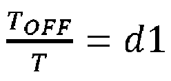


Figures 1 and3 , the power converter includes acontrol circuit 2 that is configured to operate the at least one electronic switch Q1, Q2, Q3 in each of thebridge legs control circuit 2 may be configured to generate drive signals S1, S2, S3 received by the electronic switches Q1, Q2, Q3 such that the DC link voltage V4 has a predefined voltage level and such that the inductor currents (the input currents) I1, I2, I3 essentially have the same waveform as the input voltages V1, V2, V3. For this, thecontrol circuit 2 receives a DC link voltage signal SV4, wherein the DC link voltage signal SV4 represents the DC link voltage V4. The DC link voltage V4 may be measured in a conventional way by any kind of voltage measurement circuit (not shown) in order to obtain the DC link voltage signal SV4. Further, thecontrol circuit 2 receives input voltage signals SV1, SV2, SV3, each representing a respective one of the input voltages V1, V2, V3 and input current signals SI1, SI2, SI3 each representing a respective one of the input currents I1, I2, I3. The input voltage V1, V2, V3 may be measured in a conventional way in order to obtain the input voltage signals SV1, SV2, SV3. Further, the input currents I1, I2, I3 may be measured in a conventional way in order to obtain the input current signals SI1, SI2, SI3. One example of acontrol circuit 2 configured to generate the drive signals S1-S3 is illustrated inFigure 6 . - The
control circuit 2 shown inFigure 6 includes afirst filter 21 that receives the DC link voltage signal SV4 and a DC link voltage reference signal SV4_REF, wherein the DC link voltage reference signal SV4_REF represents the desired voltage level of the DC link voltage V4. Thefilter 21 subtracts the DC link voltage reference signal SV4_REF from the DC link voltage signal SV4 and filters the difference in order to generate a DC link voltage error signal SV4_ERR. The filter (or controller) may have one of a proportional (P) characteristic, a proportional-integrative (PI) characteristic, a proportional-integrative-derivative (PID) characteristic, or the like. Amultiplier 22 receives the DC link voltage error signal SV4_ERR and the DC link voltage reference signal SV4_REF, wherein an output signal S22 of themultiplier 22 represents a desired output power of the power converter. Adivider 23 divides the multiplier output signal S22 by a signal that represents 1.5 times the square of the amplitude of the input voltages V1, V2,V3 
divider 23 represents an overall desired input current of the power converter, wherein the overall desired input current is the input current that is required by the power converter in order to achieve the desired voltage level of the DC link voltage V4 as defined by the DC link voltage reference signal SV4_REF. - Referring to
Figure 6 , thecontrol circuit 2 further includes three branches, wherein each of these branches receives the divider output signal S23 and generates a respective one of the three drive signals S1, S2, S3. Each of these branches includes a multiplier 24i, 242, 243 that multiplies the divider output signal S23 with the respective input voltage signal SV1, SV2, SV3, wherein an output signal of each of these multipliers 241, 242, 243 is an input current reference signal SI1_REF, SI2_REF, SI3_REF, that is, each of these signals SI1_REF, SI2_REF, SI§_REF represents the desired current level of a respective one of the input currents I1, I2, I3. From each of these reference signals SI1_REF, SI2_REF, SI3_REF the respective input current signal SI1, SI2, SI3 is subtracted by a respective subtractor 251, 252, 253 connected downstream the respective multiplier 241, 242, 243. The output signal of each of these subtractors 251, 252, 253 is filtered by a respective filter 261, 262, 263 connected downstream the respective subtractor 251, 252, 253, wherein an output signal SVL1_REF, SVL2_REF, SVL3_REF of the respective filter 261, 262, 263 represents a desired voltage level of a respective one of the three inductor voltages VL1, VL2, VL3. A further subtractor 271, 272, 273 subtracts the input voltage signal SV1, SV2, SV3 from the respective inductor voltage reference signal SVL1_REF, SVL2_REF, SVL3_REF in order to obtain switch node voltage reference signals SVA'_REF, SVB'_REF, SVC'_REF, wherein each of these switch node voltage reference signals SVA'_REF, SVB'_REF, SVC'_REF represents the desired voltage level of a respective one of the three leg input voltages VA', VB', VC'. - Referring to
Figure 6 , each of the three branches that generate the drive signals S1, S2, S3 includes a PWM modulator 281, 282, 283 that receives a respective one of the leg input voltage reference signals SVA'_REF, SVB'_REF, SVC'_REF, wherein each of these modulators 281, 282, 283 is configured to generate a respective one of the drive signals S1, S2, S3 based on the respective reference signal SVA'_REF', SVB'_REF, SVC'_REF such that in each drive cycle of the at least one electronic switch Q1, Q2, Q3 an average of the respective leg input voltage VA', VB', VC' equals the voltage level as defined by the respective leg input voltage reference signal SVA'_REF', SVB'_REF', SVC'_REF. The specific implementation of the PWM modulators 281, 282, 283 is dependent on the type of abridge leg - In a 3-level power converter, that is, a power converter implemented with bridge legs as illustrated in
Figure 3 andFigures 7A-7C , for example, each of the PWM modulators 281, 282, 283 may be configured to calculate the duty cycles d1, d2, d3 of the drive signals S1, S2, S3 based on one of equations (3a), (3b) or (3c) and generate the drive signals S1, S2, S3 in accordance with the calculated duty cycle. - Referring to these equations, by suitably adjusting the duty cycles d1, d2, d3 not only the switch node voltages VA', VB', VC' but also the common mode voltage VCM can be adjusted. Basically, in order to achieve a sinusoidal current waveform, the first DC link node voltage VX has to be equal to or higher than the highest voltage level of the three input voltages V1, V2, V3 and the second DC link node voltage VZ has to be equal to or lower than the lowest voltage level of the three input voltages V1, V2, V3. If, for example, it is desired that the common mode voltage VCM is zero, each of the capacitor voltages VC1, VC2 has to be higher than the amplitude of the three input voltages. Thus, when the input voltages V1, V2, V3 are 230 VRMS voltages, each of the capacitor voltages has to be higher than 325V, so that the DC link voltage has to be higher than 650V (=2*325V). If, for example, the DC link voltage is twice the amplitude of the input voltages and the common mode voltage VCM is zero, the duty cycles d1, d2, d3 as defined by equations (3a), (3b) and (3c), in the steady state, essentially follow the respective input voltage V1, V2, V3.
- In some cases, however, it may be desirable to regulate the DC link voltage V4 to a voltage level that is lower than twice the amplitude of the input voltages V1, V2, V3. This can be achieved by suitably adjusting the common mode voltage VCM. In the example illustrated in
Figure 4 , the common voltage VCM (which is not illustrated) has been selected such that it equals -(Vmax'+Vmin')/2, wherein Vmax' denotes the voltage level of the highest one of the three switch node voltages VA', VB', BC' at a certain time instance, that is Vmax'=max{ VA'; VB'; BC'}, and Vmin' denotes the lowest one of the three switch node voltages at a certain time instance, that is Vmin'=min{ VA'; VB'; BC'}. In the steady state, the switch node voltages VA', VB', BC' follow the input voltages V1, V2, V3 and can be considered to be essentially equal to the input voltages V1, V2, V3 (the inductor voltages VL1, VL2, VL3 are low as compared to the input voltages V1, V2, V3). In order to adjust the duty cycles, the PWM modulators 28i, 282, 283 may each receive a common mode voltage signal SVCM that represents the desired common mode voltage. This common mode signal SVCM may be provided by a central controller (which is not illustrated). This central controller may be a microcontroller or the like. - In the method illustrated in
Figure 4 , the electronic switch Q1, Q2, Q3 in each of thebridge legs - Referring to the above, the
bridge legs first bridge leg 11 in the following. The second andthird bridge leg 12. 13 can be implemented in the same way as thefirst bridge leg 11.Figure 7A illustrates a first example of thefirst bridge leg 11- In this example, thefirst bridge leg 11 is implemented in the way explained with reference toFigure 3 . That is, thebridge leg 11 includes a bidirectional blocking switch Q1 connected between the first switch node A' and the midpoint Y, a first rectifier element D11 connected between the first switch node A' and the first DC link node X, and a second rectifier element D12 connected between the second DC link node Z and the first switch node A'. - A second example for implementing the
first bridge leg 11 is illustrated inFigure 7B . In this example, thebridge leg 11 includes a first rectifier element D211 connected to the first DC link node X, a second rectifier element D212 connected to the second DC link node Z, a third rectifier element D213 connected between the switch node A' and the first rectifier element D211, a fourth rectifier element D214 connected between the switch node A' and the second rectifier element D212, a fifth rectifier element D215 connected between the midpoint Y and the first rectifier element D211, and a sixth rectifier element D216 connected between the midpoint Y and the second rectifier element D212. Further, an electronic switch Q1 is connected between the first and second rectifier elements D211, D212. This electronic switch Q1 may be a unidirectional electronic switch such as, for example, a MOSFET. Referring toFigure 7B , the rectifier elements D211-D216 may be implemented as diodes. These rectifier elements D211-D216 are connected such that during the positive halfwave of the first input voltage V1, the inductor current I1 can flow from the first switch node A' via the third rectifier element D213, the electronic switch Q1 and the sixth rectifier element D216 to the midpoint Y, when the electronic switch Q1 is switched on. When the electronic switch Q1 is switched off, the inductor current I1 flows via the third rectifier element D213 and the first rectifier element D211. During the negative halfwave of the input voltage V1, the current flows from the midpoint Y via the fifth rectifier element D215 and the fourth rectifier element D214 to the first switch node A' when the electronic switch Q1 is switched on. When the electronic switch Q1 is switched off, the current flows from the second DC link node Z via the second rectifier element D212 and the fourth rectifier element D214 to the first switch node A'. -
Figure 7C shows a third example of thefirst bridge leg 11. In this example, thefirst bridge leg 11 includes a first rectifier element D311 connected to the first DC link node X, a second rectifier element D312 connected to the second DC link node Z, a first switch Q311 connected between the first switch node A' and the first rectifier element D311, a second switch Q312 connected between the first switch node A' and the second rectifier element D312, a third rectifier element D313 connected between the midpoint Y and the first rectifier element D311, and a fourth rectifier element D314 connected between the midpoint Y and the second rectifier element D312. - The electronic switches Q311, Q312 may be unidirectional blocking switches such as, for example, MOSFETs. The electronic switches Q311, Q312 and the rectifier elements D311-D314 may be connected such that during the positive halfwave of the input voltage V1 the inductor current I1 flows via the switch node A' via the second electronic switch Q312 and the fourth rectifier element D314 to the midpoint Y when the second electronic switch Q312 is switched on. When the second electronic switch Q312 is switched off, the inductor current I1 flows via the first electronic switch Q311 and the first rectifier element D311 to the first DC link node X. The first electronic switch Q311, Q312 may be switched on and off at the same time. In this case, during the off-period, the inductor current I1 flows via the body diode of the MOSFET forming the first electronic switch Q311 and the first rectifier element D311. According to another example, the first and second electronic switch Q311, Q312 are operated in a complementary fashion, so that only one of the switches is switched on at the same time. In this case, the first switch Q311 is switched on when the second switch Q312 switches off, so that the inductor current I1 flows via the switched on first electronic switch Q311 and the first rectifier element D311.
- During the negative halfwave of the input voltage V1, the inductor current I1 flows from the midpoint Y via the third rectifier element D311 and the first electronic switch Q311 to the first switch node A' when the first electronic switch Q311 is switched on. When the first electronic switch Q311 is switched off, the inductor current I1 flows from the second DC link node Z via the second rectifier element D311 and the second electronic switch Q312 to the first switch node A'.
-
Figure 7D shows a modification of thebridge leg 11 shown inFigure 7C . In the example shown inFigure 7D the first switch Q311 is connected between the midpoint Y and the first rectifier element D311, the second switch Q312 is connected between the midpoint Y and the second rectifier element D312, the third rectifier element D313 is connected between the switch node A' and the first rectifier element D311, and the fourth rectifier element D314 is connected between the switch node A' and the second rectifier element D311. - Each of the
bridge legs 11 shown inFigures 7A, 7B ,7C and 7D is configured to provide three different voltage levels at the first switch node A'. Using one of thebridge legs 11 shown inFigures 7A to 7D , the average electrical potential at the first switch node A' during one drive cycle is generated from two voltage levels, the electrical potential VX at the first DC link node X and the electrical potential VY at the midpoint Y during the positive halfwave at the input voltage V1, and the electrical potential VZ at the second DC link node Z and the electrical potential VY at the midpoint Y during the negative halfwave of the input voltage V1. -
Figures 7E and 7F illustrate further examples of thefirst bridge leg 11. In these examples, thebridge leg 11 includes capacitors in addition to DC link capacitors C1, C2. In these examples, in each of the positive halfwave and the negative halfwave of the input voltage V1, more than two different voltage levels are available for generating the switch node voltage VA' such that it assumes the desired value. Thebridge legs 11 illustrated inFigures 7D and7E are so-called multi-level bridge legs, wherein thebridge leg 11 shown inFigure 7D is a Hybrid Active Neutral Point Clamped Converter leg, and thebridge leg 11 shown inFigure 7E is a Stacked Multicell Converter leg. These legs are known (see, for example, G. Gateau, T.A. Meynard, H. Foch: " Stacked Multicell Converter (SMC): Properties and design", 2001 IEEE 32nd Annual Power Electronics Specialists Conference, Vol. 3, pages 1583-1588), so that no further explanation is required in this regard. Basically, each of these bridge legs is capable of providing more than three different voltage levels, that is, the three voltage levels VX, VY, VZ and additional voltage levels for generating the switch node voltage VA'. - In the examples illustrated in
Figures 7A-7F , the rectifier elements may be implemented as diodes (as illustrated). This, however, is only an example. According to another example (not shown) these rectifier elements may be implemented as synchronous rectifier elements. - Referring to the above, operating a power converter of the type illustrated in
Figures 1 and3 may include a PWM (pulse-width modulated) operation of each of the at least one electronic switch in each of thebridge legs - According to one example, reducing switches losses includes operating the power converter in a reduced switching mode, wherein operating the power converter in a reduced switching mode includes deactivating the at least one switch Q1, Q2, Q3 in one or two of the
bridge legs bridge leg bridge leg 11 with one electronic switch is illustrated inFigure 7A wherein, as illustrated inFigure 5 , one switch may include two transistors.Bridge legs 11 with several (unidirectional blocking) switches are illustrated inFigures 7B-7F . In a bridge leg with several switches, "deactivating the at least one switch" includes deactivating each of the several switches. Further, as used herein, "the at least one electronic switch" is a switch that is used in a respective bridge leg to connect the switch node to the midpoint Y or to a circuit node having a voltage between the voltage at the midpoint Y and one of the first and second DC link node voltages VX, VZ. Voltages between the voltage at the midpoint Y and one of the first and second DC link node voltages VX, VZ are provided in the bridge legs illustrated inFigures 7E and 7F , for example. Referring to the above, the rectifier elements that couple the switch nodes A', B', C' to the first and second DC link nodes X, Z may include an electronic switch. Thus, "deactivating the at least one switch", does not include deactivating electronic switches acting as (synchronous) rectifiers. - One example of operating the power converter in a reduced switching mode is illustrated in
Figure 8 , whereinFigure 8 illustrates signal diagrams of the drive signals S1, S2, S3, the input voltages V1, V2, V3, the DC link voltage V4, the input currents I1, I2, I3, the currents ID11, ID12, IQ11 in thefirst bridge leg 11 and the voltage VQ1 across the first switch Q1 in thefirst bridge leg 11. The operating mode illustrated inFigure 8 is referred to as 1/3 mode in the following. In this operating mode, there are time periods in which only one of the threebridge legs bridge legs bridge legs - In the example shown in
Figure 8 , the power converter is operated in the 1/3 mode throughout the period of the input voltages V1, V2, V3. That is, at each time of the period of the input voltages V1, V2, V3 only one of thebridge legs - Referring to the above, the switch node voltage of a deactivated bridge leg is either clamped to the DC link voltage VX at the first DC link node X or the DC link voltage VZ at the second DC node Z. Thus, in the 1/3 mode, the switch node voltage of one bridge leg is clamped to the first DC link node voltage VX, and the switch node voltage of another bridge leg is clamped to the second DC link node voltage VZ. The bridge legs that are deactivated change over one period of the input voltage system. This is explained with reference to signal diagrams illustrated in
Figure 13 herein further below.. - According to one example, the currents through the two inductors that are connected to the deactivated bridge legs are regulated by suitably regulating the DC link voltage V4 by a
further power converter 5 connected to the DC link nodes X, Z of the power converter. A power converter arrangement with a power converter of the type explained before and afurther power converter 5 connected to the DC link nodes X, Z of the power converter is illustrated inFigure 10 . Thepower converter 10 is also referred to as first power converter and thefurther power converter 5 is also referred to as second power converter in the following. Thesecond power converter 5 may be configured to provide a constant output current IOUT or a constant output voltage VOUT different from the DC link voltage V4. When thesecond power converter 5 contributes to the regulation of the inductor currents I1, I2, I3 in thefirst power converter 10 by suitably regulating the DC link voltage V4 there is no increase of the losses occurring in thesecond power converter 5. The switching losses in the first power converter, however, are significantly reduced. Thus, there is a synergy between the control of the first power converter and the control of thesecond power converter 5. - One example of a
control circuit 4 configured to operate a power converter arrangement with a first power converter and a second power converter of the type shown inFigure 9 is illustrated inFigure 10 . Thecontrol circuit 4 shown inFigure 10 includes two main branches (or subcircuits), afirst branch 40 configured to operate the first power converter and asecond branch 6 configured to operate thesecond power converter 5. It should be noted that the block diagram shown inFigure 10 illustrates the functional blocks of thecontrol circuit 4 rather than a specific implementation. Those functional blocks can be implemented in various ways. According to one example, these functional blocks are implemented using dedicated circuitry. According to another example, thecontrol circuit 4 is implemented using hardware and software. For example, the first control circuit includes a microcontroller and software executed by the microcontroller. - For the purpose of explanation it is assumed that in the power converter arrangement illustrated in
Figure 10 the output current IOUT of thesecond power converter 5 is regulated and that the output voltage VOUT is defined by a load (not shown) receiving the output current. The load may be a battery that receives the output current IOUT and defines the output voltage VOUT. - The
first branch 40 of thecontrol circuit 4 shown inFigure 10 is based on the control circuit shown inFigure 6 , wherein the same elements have the same reference characters. Referring toFigure 10 , thecontrol circuit 4 receives an output current signal SIOUT wherein the output current signal SIOUT represents the output current IOUT. The output current IOUT may be measured in a conventional way by any kind of current measurement circuit (not shown) in order to obtain the output current signal SIOUT. Thecontrol circuit 4 includes afirst filter 41 that receives the output current signal SIOUT and an output current reference signal SIOUT_REF, wherein the an output current reference signal SIOUT REF represents the desired current level of the output current IOUT. Thefirst filter 41 subtracts the output current reference signal SIOUT REF from the output current signal SIOUT, for example, and filters the difference in order to generate an output signal SV51_REF. According to one example, this output signal SV51_REF represents a desired voltage V51 across aninductor 51 in thesecond power converter 5, wherein thisinductor 51 carries the output current IOUT. One example ofsuch inductor 51 is illustrated inFigure 9 . - The filter may have one of a proportional (P) characteristic, a proportional-integrative (PI) characteristic, a proportional-integrative-derivative (PID) characteristic, or the like. A
adder 42 receives the filter output signal SV51_REF and an output voltage signal SVOUT that represents the output voltage VOUT, wherein an output signal S42 of theadder 42 and the filter output signal SV51_REF are received by a multiplier. An output signal S43 of themultiplier 43 represents a desired output power of the power converter arrangement. Thedivider 23 already explained withFigure 6 divides the multiplier output signal S43 by a signal that represents 1.5 times the square of the amplitude of the input voltages V1, V2, V3 (
divider 23 represents an overall desired input current of the first power converter. The divider output signal S23 is processed by the three branches explained with reference toFigure 6 before in order to generate the three switch node voltage reference signals SVA'_REF, SVB'_REF, SVC'_REF. It should be noted that the current control loop is the slowest one of the control loops explained in context withFigure 10 . - Controlling the output current IOUT by the
control circuit 4 is only an example. According to another example, the output voltage VOUT is controlled. In this example (not shown), thefilter 41 receives the output voltage signal SVOUT and an output voltage reference signal SVOUT_REF representing the desired voltage level of the output voltage VOUT. Further, theadder 42 is omitted and themultiplier 43 receives the output signal from thefilter 41 and the output voltage reference signal SVOUT_REF. - Referring to
Figure 10 , aPWM modulator 44 receives the switch node voltage reference signals SVA'_REF, SVB'_REF, SVC'_REF. From these switch node voltage reference signals SVA'_REF, SVB'_REF, SVC'_REF the PWM modulator 44 (a) selects a maximum and deactivates the bridge leg associated with the maximum voltage reference signal; (b) selects a minimum and deactivates the bridge leg associated with the minimum voltage reference signal; and (c) operates the remaining bridge leg in the PWM mode. The "remaining bridge leg" is the bridge leg, associated with the switch node reference signal that is between the maximum and the minimum switch node voltage reference signal. This switch node voltage reference signal is referred to as intermediate switch node voltage reference signal in the following. - The
second branch 6 of the control circuit also receives the three switch node voltage reference signals SVA'_REF, SVB'_REF, SVC'_REF and is configured to control operation of thesecond power converter 5 based on these signals SVA'_REF, SVB'_REF, SVC'_REF. One example of thesecond branch 6 of the control circuit is explained in detail herein further below. -
Figure 11 illustrates one example of thesecond power converter 5. In this example, thesecond power converter 5 includes afirst converter stage 51 and asecond converter stage 52, wherein each of these a first and second converter stages 51, 52 includes afirst input node second input node first output node second output node first input node 511 of thefirst converter stage 51 may be connected to the first DC link node X, thesecond input node 522 of thesecond converter stage 52 may be connected to the second DC link node Z, and thesecond input node 512 of thefirst converter stage 51 and thefirst input node 521 of thesecond converter stage 52 may be connected with each other and connected to the midpoint Y. Further, thesecond output node 514 of thefirst converter stage 51 and thefirst output node 523 of thesecond converter stage 52 may be connected with each other. The output voltage VOUT is the voltage between thefirst output node 513 of thefirst converter stage 51 and thesecond output node 524 of thesecond converter stage 52. - The converter stages 51, 52 may each be implemented with one of various different converter topologies. According to one example, each of the converter stages 51, 52 is implemented as an isolated DC-DC converter, that is, a DC-DC converter that includes a transformer between the
respective input respective output respective input respective output second converter stage - One example of the
second converter branch 6 configured to control operation of asecond power converter 5 of the type shown inFigure 11 is illustrated inFigure 12 . Thiscontrol circuit 6 includes a maximum andminimum selector 61 that receives the three switch node voltage reference signals SVA'_REF, SVB'_REF, SVC'_REF. This maximum andminimum selector 61 is configured to select the maximum of switch node voltage reference signals SVA'_REF, SVB'_REF, SVC'_REF and the minimum of the switch node voltage reference signals SVA'_REF, SVB'_REF, SVC'_REF and output a first signal SMAX' that equals the maximum of the switch node voltage reference signals SVA'_REF, SVB'_REF, SVC'_REF, and a second signal SMIN' that equals the minimum of the switch node voltage reference signals SVA'_REF, SVB'_REF, SVC'_REF, so that SMAX' = max{ SVA'_REF, SVB'_REF, SVC'_REF} and SMIN' = max{ SVA'_REF, SVB'_REF, SVC'_REF}. The first signal SMAX' is also referred to as maximum switch node voltage reference signal SMAX', and the second signal SMIN' is also referred to as minimum switch node voltage reference signal. The intermediate switch node voltage reference signal is also referred to as SINT' in the following. - The second
control circuit branch 6 is configured to operate thesecond power converter 5 in such a way that the DC link voltage V4 equals a voltage that is represented by the difference between the maximum switch node voltage reference signal SMAX' and the minimum switch node voltage reference signal SMIN'. Referring to the above, the switch nodes of the bridge legs that are deactivated are clamped to the first DC link node voltage VX and the second DC link node voltage VZ, respectively. By adjusting the DC link voltage V4 such that it equals a voltage represented by the difference between the maximum switch node voltage reference signal SMAX' and the minimum switch node voltage reference signal SMIN' the switch nodes that are clamped to the first and second DC link nodes X, Z receive the switch node voltages calculated by the firstcontrol circuit branch 40. Thus, the inductor currents of those inductors connected to deactivated bridge legs have a current level as represented by the respective input current reference signal calculated by the firstcontrol circuit branch 40. - Referring to
Figure 12 , the secondcontrol circuit branch 6 includes asubtractor 62 that subtracts the minimum switch node voltage reference signal SMIN from the maximum switch node voltage reference signal SMAX', wherein amultiplier 63 multiplies an output signal of the subtractor with 0.5. An output signal of the multiplier forms a first capacitor voltage reference signal SVC1_REF and a second capacitor voltage reference signal SVC2_REF, wherein the first capacitor voltage reference signal SVC1_REF represents a desired value of the first capacitor voltage VC1, and the second capacitor voltage reference signal SVC2_REF represents a desired value of the second capacitor voltage VC2. The secondcontrol circuit branch 6 includes a first branch and a second branch. The first branch receives the first capacitor voltage reference signal SVC1_REF and is configured to provide a first input current reference signal SI51_REF, wherein the first input current reference signal SI51_REF represents a desired input current I51 of thefirst converter stage 51. The second branch receives the second capacitor voltage reference signal SVC2_REF and is configured to provide a second input current reference signal SI52_REF, wherein the second input current reference signal SI52_REF represents a desired input current I52 of thesecond converter stage 52. - The first branch includes a subtractor 641 that subtracts a first capacitor voltage signal SCV1, which represents the first capacitor voltage VC1, from the first capacitor voltage reference signal SVC1_REF. An output signal of the subtractor is filtered by a filter 651, wherein an output signal SIC1_REF of the filter represents a desired current level of a current into the first capacitor C1. The first input current reference signal SI51_REF is given by a difference between a current signal Six that represents a current into the first DC link node X (wherein this current IX is provided by the first power converter) and the filter output signal SIC1_REF.
- The second branch includes a subtractor 642 that subtracts a second capacitor voltage signal SCV2, which represents the second capacitor voltage VC2, from the second capacitor voltage reference signal SVC2_REF. An output signal of the subtractor is filtered by a filter 652, wherein an output signal SIC2_REF of the filter represents a desired current level of a current into the second capacitor C2. The second input current reference signal SI52_REF is given by a difference between a current signal SIZ that represents a current into the second DC link node Z (wherein this current IZ is provided by the first power converter) and the filter output signal SIC2_REF.
- Referring to
Figure 12 , a first PWM modulator 671 receives the first input current reference signal SI51_REF and a first input current signal SI51, wherein the latter represents the first input current 151, and is configured to control operation of one or more switches (not shown in the figures) included in thefirst converter stage 51 such that the first input current I51 has a current level as represented by the first input current reference signal SI51_REF. Equivalently, a second PWM modulator 67i receives the second input current reference signal SI52_REF and a second input current signal SI52, wherein the latter represents the second input current I52, and is configured to control operation of one or more switches (not shown in the figures) included in the second converter stage 52 (not shown in the figures) such that the first input current 151 has a current level as represented by the first input current reference signal SI51_REF. The specific implementation of the PWM modulators 671, 672 is dependent on the specific type of power converter used to implement the first and second converter stages 51, 52. However, PWM modulators configured to control the input current in various kinds of DC-DC converters are known, so that no further explanations are required in this regard. - Referring to the above, activating one of the three
bridge legs other bridge legs PWM modulator 44 in the 1/3 mode is dependent on the switch node voltage reference signals SVA'_REF, SVB'_REF, SVC'_REF. Time instances at which two of these switch node voltage reference signals SVA'_REF, SVB'_REF, SVC'_REF are equal can be neglected, so that at each time, from these switch node voltage reference signals SVA'_REF, SVB'_REF, SVC'_REF, one forms the maximum switch node voltage reference signal SMAX', one forms the intermediate switch node voltage reference signal SINT', and one forms the minimum switch node voltage reference signal SMIN'. This is explained with reference toFigure 13 in greater detail. -
Figure 13 illustrates signal diagrams of switch node voltage reference signals SVA'_REF, SVB'_REF, SVC'_REF, wherein each of these signals represents the desired voltage value of the respective switch node voltage VA', VB', VC'.Figure 13 further illustrates which of the bridge legs is operated in the PWM mode at which time or phase angle. Referring to the above and as illustrated inFigure 13 , in the steady state, each of the switch node voltage reference signals SVA'_REF, SVB'_REF, SVC'_REF follows the respective input voltage. - Referring to
Figure 13 , a relationship between the individual switch node voltage reference signals SVA'_REF, SVB'_REF, SVC'_REF changes several times within one period. The "relationship" means the signal level of one of the switch node voltage reference signals SVA'_REF, SVB'_REF, SVC'_REF relative to the signal levels of the other two of the switch node voltage reference signals SVA'_REF, SVB'_REF, SVC'_REF. In the example illustrated inFigure 13 , there are six time periods P1-P6, which are also referred to as operating phases in the following, wherein in each of these time periods P1-P6 the relationship between the switch node voltage reference signals SVA'_REF, SVB'_REF, SVC'_REF does not change. (The signal levels of the switch node voltage reference signals SVA'_REF, SVB'_REF, SVC'_REF, however, vary in the individual operating phases P1-P6.) - In a first operating phase P1, for example, the first switch node voltage reference signal SVA'_REF has the highest voltage level. That is, the voltage level of the first switch node voltage reference signal SVA'_REF is higher than the voltage level of a second one SVB'_REF of the switch node voltage reference signals SVA'_REF, SVB'_REF, SVC'_REF and the signal level of a third one SVC'_REF of the switch node voltage reference signals SVA'_REF, SVB'_REF, SVC'_REF. Further, in the first operating phase P1, the second switch node voltage reference signal SVB'_REF V2 hast the lowest voltage level. That is, the voltage level of the second switch node voltage reference signal SVB'_REF is lower than the signal level of the first switch node voltage reference signal SVA'_REF and the signal level of the third switch node voltage reference signal SVC'_REF. Further, the third switch node voltage reference signals SVA'_REF, SVB'_REF, SVC'_REF has a signal level between the voltage level of the first switch node voltage reference signal SVA'_REF and the signal level of the second switch node voltage reference signal SVB'_REF. Thus, in the first operating phase P1, the first switch node voltage reference signal SVA'_REF is the maximum switch node voltage reference signal SMAX', the second switch node voltage reference signal SVB'_REF is the minimum switch node voltage reference signal SMIN', and the third switch node voltage reference signal SVC'_REF is the intermediate switch node voltage reference signal SINT'_REF. In the second operating phase P2, for example, the first switch node voltage reference signal SVA'_REF is the maximum switch node voltage reference signal SMAX', the second switch node voltage reference signal SVB'_REF is the intermediate switch node voltage reference signal SINT', and the third switch node voltage reference signal SVC'_REF is the minimum switch node voltage reference signal SMIN' REF.
- In the following, the input voltage having the highest voltage level is referred to as maximum input voltage Vmax, the input voltage having the lowest voltage level is referred to as minimum input voltage Vmin, and the input voltage having a voltage level between the highest voltage level and the lowest voltage level is referred to as intermediate input voltage VINT. The line-to-line voltage VLL explained above is then given by VLL=Vmax-Vmin. Referring to the above, the switch node voltage reference signals SVA'_REF, SVB'_REF, SVC'_REF, in the steady state, essentially follow the input voltages V1, V2, V3, so that the output signal SMAX'- SMIN' of the
subtractor 62 shown inFigure 12 essentially represents the line-to-line voltage VLL. The subtractor output signal SMAX'- SMIN' is also illustrated inFigure 13 . - Referring to
Figure 13 , operating the power converter in the 1/3 mode includes activating the bridge leg associated with the intermediate voltage reference signal SINT' and deactivating the bridge legs associated with the maximum switch node voltage reference signal SMAX' and the minimum switch node voltage reference signal SMIN'. That is, in the first operating phase P1, for example, thethird bridge leg 13 is activated, in the second operating phase P2 thesecond bridge leg 12 is activated, and so on. - Referring to the above, the
bridge legs PWM modulator 44 in thecontrol circuit 4. According to one example, thePWM circuit 44 is configured to calculate the duty cycles d1, d2, d3 based on


Figure 13 over one period of the input voltages. When adjusting the duty cycles d1, d2, d3 in accordance with equations (4a)-(4c) and (5) the duty cycle of the bridge leg associated with the maximum switch node voltage reference signal SMAX' is "automatically" set to +1 throughout the respective operating phase, so that the respective switch node is clamped to VX. Further, the duty cycle of the bridge leg associated with the minimum switch node voltage reference signal SMIN' is "automatically" set to -1 throughout the respective operating phase, so that the respective switch node is clamped to VZ. This is explained in the following. - In the following, dmax denotes the duty cycle of the bridge leg associated with the maximum switch node voltage reference signal SMAX' in a respective operating phase, and dmin denotes the duty cycle of the bridge leg associated with the minimum switch node voltage reference signal SMIN' in a respective operating phase. Further, Vmax' denotes the desired switch node voltage represented by the maximum switch node voltage reference signal SMAX', and Vmin' denotes the desired switch node voltage represented by the minimum switch node voltage reference signal SMIN'. Based on one of equations (4a)-(4c) and equation (5) and considering that the DC link voltage V4 is adjusted such that V4=Vmax'-Vmin', the duty cycle dmax and the duty cycle dmin are given by


- Referring to the above, when the
first power converter 10 is operated in the 1/3 mode, the DC link voltage V4 is adjusted by thesecond converter 5 such that it equals Vmax'-Vmin', wherein Vmax' is the maximum of the desired switch node voltages and Vmin' is the minimum of the desired switch node voltages. In the steady state, these desired switch node voltages Vmax', Vmin' essentially equal the maximum input voltage Vmax and the minimum input voltage Vmin, respectively, so that the varying DC link voltage V4 essentially equals the line-to-line voltage VLL. This is the lowest possible DC link voltage at which sinusoidal input currents I1, I2, I3 can be achieved, wherein the common mode voltage VCM is different from zero and given by equation (5) in this case. - The power converter arrangement illustrated in
Figure 9 is not restricted to generate the DC link voltage V4 such that it is defined by SMAX'-SMIN' and essentially equals the line-to-line voltage VLL.Figure 14 illustrates one example of a secondcontrol circuit branch 6 that is configured to generate the DC link voltage V4 such that in some time periods it is defined by the subtractor output signal S62 (=SMAX'-SMIN') and in some time periods is higher than defined by the subtractor output signal S62.. In this example, amaximum selector 68 receives the subtractor output signal S62 and a minimum DC link voltage signal SV4_MIN, wherein the minimum DC link voltage signal SV4_MIN represents the minimum of the DC link voltage V4 that should be generated at the output of thefirst power converter 10. The maximum selector outputs the maximum of the two signal it receives to themultiplier 63. The voltage represented by the minimum DC link voltage signal SV4_MIN is referred to as minimum desired DC link voltage V4MIN in the following. - When the minimum desired DC link voltage V4MIN is the minimum of the subtractor output signal S62 or below, the DC link voltage is generated as explained above and the
first power converter 10 is operated in the full 1/3 mode, that is, the power converter operates in the 1/3 mode throughout each of the six operating phases. This type of operating mode is again illustrated inFigure 15 , whereinFigure 15 illustrates operating the power converter in the full 1/3 mode between a first time instance t1 and a second time instance t2. - When the minimum desired DC link voltage signal SV4_MIN is higher than a minimum of the subtractor output signal S62, the DC link voltage V4 is generated such that it is generated based on the subtractor output signal S62 in time periods in which the subtractor output signal S62 is higher than the minimum desired DC link voltage signal SV4_MIN. In the remainder of the time the DC link voltage V4 is generated based on the minimum desired DC link voltage signal SV4_MIN. In this type of operation, the power converter is not operated in the 1/3 mode throughout each of the six operating phases anymore. Instead there are time periods in which the first power converter is operated in the 1/3 mode, but also time periods in which each of the
bridge legs Figure 15 . - Between these time instances t2, t3 the minimum desired DC link voltage increases V4MIN in order to illustrate how operation of the power converter changes dependent on the desired DC link voltage V4MIN. The minimum desired DC link voltage V4MIN is the minimum of the DC link voltage V4, which is also illustrated in
Figure 15 . Basically, as can be seen fromFigure 15 , the duration in which the power converter operates in the 1/3 mode during one period of the input voltages V1, V2, V3 decreases as the minimum DC link voltage V4MIN increases. The operating mode in which the power converter alternatingly operates in the 1/3 mode and the 3/3 mode (as illustrated between time instances t2 and t3 inFigure 15 ) is referred to as partial-boost mode in the following. - When calculating the duty cycles d1, d2, d3 in accordance with equations (4a)-(4c), the power converter automatically changes between the 1/3 mode and the 3/3, because these duty cycles are dependent on the DC link voltage V4 that is adjusted by the
second power converter 5. In the partial-boost mode, the common mode voltage VCM may be the same as in the full 1/3 mode. However, in those time periods in which the power converter, in the partial-boost mode, operates in the 3/3 mode the common mode voltage VCM may be different from the common mode voltage in the 1/3 mode. Only in the full 1/3 mode, the common mode voltage VCM is constrained to the value presented in equation (5). In the partial-boost mode and the full-boost mode, however, there is a degree of freedom to adjust the common mode voltage VCM such that it is different from the value given in equation (5). In these operating modes, the degree of freedom that is available to adjust the common mode voltage VCM may be used to adjust the common mode voltage VCM such that a current IY into the midpoint is minimized. This is explained in detail herein further below. -
Figure 16 illustrates the different operating modes of thefirst power converter 10 dependent on the minimum desired DC link voltage signal SV4_MIN and the phase angle of the input voltages V1, V2, V3. More specifically,Figure 16 illustrates the different operating modes in an arbitrary one of the six operating phases P1-P6, wherein each of these operating phases covers 60° of one period of the input voltages V1, V2, V3. InFigure 16 , a phase angle of 0° represents the beginning of the respective operating phase, a phase angle of 60° represents the end of the respective operating phase, and a phase angle of 30° represents the middle of the respective operating phase, which is when the intermediate input voltage in the respective operating phase crosses zero. - Referring to
Figure 16 , the power converter operates in the full 1/3 mode when the minimum desired DC link voltage signal SV4_MIN is below a minimum of the subtractor output signal S62. Referring to the above, in the steady state, the subtractor output signal S62 essentially represents the line-to-line voltage VLL, so that the power converter operates in the full 1/3 mode when the minimum desired DC link voltage V4MIN is below the minimum line-to-line voltage VLL_MIN. - Further, referring to
Figure 16 , the power converter operates in the partial-boost mode when the minimum desired DC link voltage signal SV4_MIN is between the minimum of the subtractor output signal S62 and a maximum of the subtractor output signal S62. In the steady state, the maximum of the subtractor output signal S62 essentially equals the maximum line-to-line voltage VLL_MAX, so that the power converter operates in the in the partial-boost mode when the DC link voltage V4 is between the minimum line-to-line voltage VLL_MIN and the maximum line-to-line voltage VLL_MAX. In the partial-boost mode, the portion of the operating phase in which the power converter operates in the 3/3 mode increases as the minimum desired DC link voltage V4MIN increases and the portion of the operating phase in which the power converter operates in the 1/3 mode decreases as the minimum desired DC link voltage V4MIN increases. - Referring to
Figure 16 , the power converter operates in the full 3/3 mode when the minimum desired DC link voltage signal SV4_MIN is higher than the maximum of the subtractor output signal S62. In this operating mode, the DC link voltage V4 is essentially constant and only dependent on the minimum desired DC link voltage signal SV4_MIN. - In the control circuits illustrated in
Figures 12 and14 , theinput currents 151, I52 are controlled such that each of the first and second capacitor voltages VC1, VC2 equals 50% of the desired DC link voltage V4. This, however, is only an example. According to another example illustrated inFigure 17 , the input currents I51, I52 are controlled such that the first capacitor voltage equals k1 times the desired DC link voltage V4, and the second capacitor voltage equals k2 times the desired DC link voltage V4, wherein k1+k2=1, k1>0, k2>0. In this case, the first and second capacitor voltages VC1 and VC2 are different. In this case, the duty cycles d1, d2, d3 may be calculated based on equations (3a) and (3b) by thePWM modulator 44 in thecontrol circuit 4. Optionally, the secondcontrol circuit branch 6 may include a maximum selector of the type explained with reference toFigure 14 . - In the examples illustrated in
Figures 12 ,14 and17 , the first and second converter stages 51, 52 do not only regulate the DC link voltage V4, but do also regulate the first and second capacitor voltages VC1, VC2. According to another example illustrated inFigure 18 , abalancing circuit 7 regulates a ratio between the first capacitor voltage VC1 and the second capacitor voltage VC2. In this case, the first and second converter stages 51, 52 only regulate the DC link voltage V4. Moreover, in this case, the twoconverter stages - Referring to
Figure 19 , the balancing circuit may include afirst switch 71 connected between the first DC link node X and aninductor 73 connected to the midpoint Y, andsecond switch 72 connected between the second DC link node Z and theinductor 73. Acontrol circuit 74 receives the first capacitor voltage signal Svci and the second capacitor voltage signal SVC2 and is configured to control operation of the first andsecond switches second switches second switch 72 is switched off) energy is taken from the first DC link capacitor C1, stored in theinductor 73, and transferred to the second DC link capacitor C2 when the first switch switches off and thesecond switch 72 switches on. A duty cycle of operating the twoswitches switches - Referring to the above, in the power converter arrangement shown in
Figure 10 , the DC link voltage is adjusted by thesecond power converter 5, wherein an output voltage VOUT of the second power converter may be defined by a load, such as battery that is charged by the power converter arrangement. Further, the DC link voltage V4 may be adjusted by the minimum DC link voltage signal SV4_MIN explained above. Adjusting the DC link voltage V4 may be helpful in order to achieve a high converter efficiency of the second power converter. Basically, the lower a difference between an input voltage and an output voltage of a power converter, the higher the efficiency. Thus, according to one example, the minimum DC link voltage signal SV4_MIN may be adjusted based on the output voltage VOUT such that the minimum desired DC link voltage V4MIN increases as the output voltage VOUT increases. - Another example of reduced switching mode is referred to as 2/3+PWM mode and is explained in the following. In this type of operating mode, the
power converter 10 either operates in a 2/3 mode in which one of thebridge legs bridge legs bridge legs power converter 10 of the type illustrated inFigures 1 and3 , the sum of the input currents I1, I2, I3 is zero, that is I1+I2+I3=0. Thus, by regulating two of the three input currents I1, I2, I3 the third one of the three input currents I1, I2, I3 is automatically regulated. Thus, the power converter may be operated in such a way that at each time one of thebridge legs bridge legs - In the 3/3 mode, the midpoint current IY, which is also referred to as common mode current in the following, may be reduced by suitably selecting the common mode voltage VCM. The midpoint current IY may even be reduced to zero by suitable selecting the common mode voltage, given that the common mode voltage that can be inserted is high enough. In the following, VCMzmc denotes the zero midpoint current (ZMC) common mode voltage, which is the common mode voltage at which the midpoint current IY is zero. The ZMC common mode voltage VCMzmc is given by

- On the other hand, in order to achieve sinusoidal input currents I1, I2, I3 there are constraints on the first and second DC link node voltages VX, VZ such that the first DC link node voltage VX is equal to or higher than the maximum Vmax' of the desired switch node voltages VA', VB', VC' and the second DC link node voltage VZ is equal to or lower than the minimum Vmin' of the desired switch node voltages VA', VB', VC', that is




- In order to achieve a zero midpoint current and sinusoidal input voltages, the following conditions should be met by the common voltage VCM,


- According to one example, operating the power converter in the 2/3+PWM mode includes (a) operating the power converter in the 3/3 mode whenever the ZMC common mode voltage VCMzmc is within a range given by the maximum and minimum common mode voltage VCMmax, VCMmin, that is, whenever


-
Figure 20 shows signal diagrams that illustrate operating the power converter in the 2/3+PWM mode according to one example. In particular,Figure 20 illustrates the DC link voltage V4, the input voltages V1, V2, V3, the maximum and minimum common mode voltages VCMmax, VCMmin, the ZMC common mode voltage VCMzmc, the common mode voltage VCM, and the drive signals S1, S2, S3. As can be seen fromFigure 20 , the power converter operates in the PWM mode (3/3 mode) whenever the ZMC common mode voltage VCMzmc is within the range given by the maximum and the minimum common mode voltages VCMmax, VCMmin, wherein the common mode voltage VCM is adjusted such that it equals the ZMC common mode voltage VCMzmc. When the ZMC common mode voltage VCMzmc is outside the range given by the maximum and the minimum common mode voltages VCMmax, VCMmin the power converter operates in the 2/3 mode, wherein the common mode voltage VCM is adjusted such that it equals the maximum common mode voltage VCMmax when the ZMC common mode voltage VCMzmc is greater than the maximum common mode voltage VCMmax and such that it equals the minimum common mode voltage VCMmin when the ZMC common mode voltage VCMzmc is smaller than the minimum common mode voltage VCMmin. Further, referring toFigure 20 , thebridge legs bridge legs bridge legs - According to one example, this deactivation strategy is automatically achieved when calculating the duty cycles d1, d2, d3 in accordance with equations (4a), (4b), (4c) and limiting the common mode voltage VCM either to VCMmax or VCMmin, that is, adjusting the common mode voltage VCM such that it equals the maximum common mode voltage VCMmax when the ZMC common mode voltage VCMzmc is greater than the maximum common mode voltage VCMmax and such that it equals the minimum common mode voltage VCMmin when the ZMC common mode voltage VCMzmc is smaller than the minimum common mode voltage VCMmin. When the common mode voltage VCM is limited to VCMmax, the duty cycle of the bridge leg having the maximum switch node voltage Vmax' becomes +1, so that the respective bridge leg is automatically deactivated. Equivalently, when the common mode voltage VCM is limited to VCMmin, the duty cycle of the bridge leg having the minimum switch node voltage Vmin' becomes -1, so that the respective bridge leg is automatically deactivated.
-
Figure 20 further illustrates the midpoint current IY. As can be seen, the midpoint current IY is zero in the 3/3 mode and different from zero only in those time periods (at those phase angles) in which the power converter operates in the 2/3 mode. - Basically, a duration of the time periods in which the power converter operates in the 2/3 mode in one period of the input voltages is dependent on the DC link voltage V4. This is illustrated in
Figures 21 and22 . -
Figure 21 illustrates the different operating modes of thefirst power converter 10 dependent on the DC link voltage V4 and the phase angle of the input voltages V1, V2, V3. More specifically,Figure 21 illustrates the different operating modes in an arbitrary one of the six operating phases P1-P6, wherein each of these operating phases covers 60° of one period of the input voltages V1, V2, V3. InFigure 16 , a phase angle of 0° represents the beginning of the respective operating phase, a phase angle of 60° represents the end of the respective operating phase, and a phase angle of 30° represents the middle of the respective operating phase, which is when the intermediate input voltage in the respective operating phase crosses zero. - Referring to the above, the power converter may operate in the 2/3+PWM mode when the DC link voltage V4 is greater than the maximum line-to-line voltage VLL_MAX. In the 2/3+PWM mode, the portion of the operating phase in which the power converter operates in the 3/3 mode increases as the DC link voltage V4 increases and the portion of the operating phase in which the power converter operates in the 2/3 mode decreases as the minimum desired DC link voltage V4MIN increases. Further, the power converter operates in the full 3/3 mode when the DC link voltage V4 is such that the ZMC common mode voltage VCzmc is within the range given by the maximum and the minimum common mode voltage VCMmax, VCMmin throughout one period of the input voltages V1, V2, V3. A DC link voltage threshold V4FULL_3_3 at which the power converter changes from the 2/3+PWM mode to the full 3/3 mode is greater than the maximum line-to-line voltage VLLMAX and smaller than twice the amplitude of the input voltages V1, V2, V3.
- Referring to the above it would be possible to operate the power converter in the 2/3 mode at each DC link voltage V4 higher than the maximum line-to-line voltage VLL_MAX. Thus, it would be possible to operate the power converter in the 2/3 mode or the 2/3+PWM mode at DC link voltages higher than V4FULL_3_3. This, however, would increase the midpoint current IY and is therefore undesirable. Operating the power converter in the 2/3+PWM mode at DC link voltages between the maximum line-to-line voltage VLL_MAX and V4FULL_3_3, however, helps to reduce losses.
-
Figure 22 shows signal diagrams of the drive signals S1, S2, S3, the input voltages and the input currents I1, I2, I3 and of the DC link voltage in the 2/3+PWM mode and the full 3/3 mode. As can also be seen from these signal diagrams, a duration of the time periods in which the power converter operates in the 2/3 mode decrease as the DC link voltage V4 increases. - A power converter of the type illustrated in
Figure 1 or3 may be operated in the 2/3+PWM mode by a control circuit of the type illustrated inFigure 23 . This control circuit is based on the control circuit shown inFigure 6 and includes aPWM modulator 44 of the type explained hereinbefore that generates duty cycles of the drive signals S1, S2, S3 in accordance with equations (4a)-(4c). Further, a commonmode signal generator 45 is configured to generate the common mode voltage signal SVCM received by the PWM modulator in such a way that (a) the common mode voltage VCM represented by the common mode voltage signal SVCM equals the ZMC common mode voltage VCMzmc when the ZMC common mode voltage VCMzmc is within the range given by the maximum and minimum common mode voltage VCMmax, VCMmin and (b) such that the common mode voltage VCM it is within the range given by the maximum and the minimum common mode voltage VCMmax, VCMmin when the ZMC common mode voltage VCMzmc is outside this range. For calculating the maximum, minimum and ZMC common mode voltages VCMmax, VCMmin, VCMzmc in accordance with equations (7), (10a), (10b) the commonmode signal generator 45 receives the DC link voltage signal SV4 that represents the DC link voltage V4 and the switch node voltage reference signals SVA'_REF, SVB'_REF, SVC'_REF, which represent the desired switch node voltages VA', VB', VC'. - In the above explanation it has been assumed that the (first)
power converter 10 may operate in the 2/3+PWM mode when the DC link voltage V4 is higher than the maximum line-to-line-voltage VLL_MAX. When the DC link voltage V4 is higher than the maximum line-to-line-voltage VLL_MAX the power converter operates in a full-boost mode. A 2/3+PWM mode, however, may also be used when thepower converter 10 operates in the partial boost-mode explained above. This is illustrated with reference toFigures 24 and25 in the following. -
Figure 24 illustrates the different operating modes of thefirst power converter 10 dependent on the DC link voltage V4 and the phase angle of the input voltages V1, V2, V3 in an arbitrary one of the six operating phases P1-P6. Referring to the above, the power converter operates in the partial-boost mode when the DC link voltage V4 is essentially between the minimum line-to-line voltage VLL_MIN and the maximum line-to-line voltage VLL_MAX. In the example illustrated inFigure 24 , in the partial-boost mode, the power converter either operates in the 1/3 mode, the 2/3 mode or the 3/3 mode, wherein a phase angle range (a duration of a time period) in which the power converter operates in the 1/3 mode decreases and in which the power converter operates in the 2/3 or the 3/3 mode increases as the DC link voltage V4 increases. -
Figure 25 shows corresponding signal diagrams that illustrate operating the power converter in the partial-boost mode and the 2/3+PWM mode. - Operating the
first power converter 10 in a partial boost mode of the type illustrated inFigures 23 and24 may be achieved by a control circuit of the type illustrated inFigure 10 when the common mode voltage signal SVCM is generated by a common modevoltage signal generator 45 of the type explained with reference toFigure 22 . In this case, when the DC link voltage V4 is generated by thesecond power converter 5 such that it equals the voltage represented by Smax'-Smin' the common modevoltage signal generator 45 automatically generates the common mode signal automatically such that the common mode voltage VCM is in accordance with equation (5), which is the common mode voltage used in the 1/3 mode. - Some of the aspects explained above are briefly summarized in the following with reference to numbered examples.
- Example 1. A method, comprising: operating a power converter in a reduced switching mode, wherein the power converter comprises: three input nodes each configured to receive a respective one of three input voltages; two DC link nodes configured to provide a DC link voltage, and a midpoint coupled to each of the two DC link nodes; three inductors each connected to a respective one of the three input nodes; and a rectifier bridge comprising three bridge legs each coupled to a respective one of the three inputs through a respective one of the three inductors and connected to the respective one of the three inductors at a respective switch node, wherein each of the three bridge legs is connected to the two DC link nodes and the midpoint, and comprises at least one electronic switch, and wherein operating the power converter in the reduced switching mode comprises: deactivating at least one of the three bridge legs for a predefined time period.
- Example 2. The method of
claim 1, wherein operating the power converter in the reduced switching mode comprises operating the power converter in a 1/3 mode, and wherein operating the power converter in the 1/3 mode comprises deactivating two of the three bridge legs and activating one of the bridge legs for a certain portion of a period of the input voltages. - Example 3. The method of
claim 2, further comprising: operating the power converter in the 1/3 mode throughout the period of the three input voltages. - Example 4. The method of
claim 2, further comprising: operating the power converter in the 1/3 mode in a certain portion of the period of the three input voltages. - Example 5. The method of
claim 3, further comprising: operating the power converter in a 3/3 mode, in which none of the bridge legs is deactivated, in the remainder of the period of the three input voltages. - Example 6. The method of
claim 3, further comprising: operating the power converter in a 2/3 mode, in which one of the bridge legs is deactivated, or in a 3/3 mode, in which none of the bridge legs is deactivated, in the remainder of the period of the three input voltages. - Example 7. The method of any one of
claims 2 to 6, wherein operating the power converter in the 1/3 mode further comprises: calculating a desired switch node voltage for each of the bridge legs; deactivating the one of the bridge legs associated with a maximum of the desired switch node voltages; and deactivating the one of the bridge legs associated with a minimum of the desired switch node voltages. - Example 8. The method of
claim 7, wherein the method further comprises regulating the DC link voltage by a further power converter. - Example 9. The method of claim 8, wherein each of the desired switch node voltages is dependent on an output parameter of the further power converter and a respective one of the input voltages, and wherein regulating the DC link voltage by the further power converter comprises regulating the DC link voltage dependent on a difference between a maximum of the desired switch node voltages and a minimum of the desired switch node voltages.
- Example 10. The method of claim 9, wherein the output parameter is an output current of the second power converter.
- Example 11. The method of claim 9, wherein the output parameter is an output voltage of the second power converter.
- Example 12. The method of claim 9, wherein the method further comprises: adjusting a switch node voltage of an activated one of the bridge legs by a switched-mode operation of the at least one electronic switch in the activated bridge leg dependent on the desired switch node voltage associated with the activated bridge leg.
- Example 13. The method of
claim 1, wherein operating the power converter in the reduced switching mode comprises operating the power converter in a 2/3 mode, and wherein operating the power converter in the 2/3 mode comprises deactivating one of the three bridge legs and activating two of the bridge legs for a certain portion of a period of the input voltages. - Example 14. The method of
claim 13, wherein operating the power converter in the 2/3 mode comprises: calculating a zero midpoint current common mode voltage, a minimum desired common mode voltage, and maximum desired common mode voltage; and operating the power converter in the 2/3 mode when the common mode voltage is outside a voltage range defined by the minimum desired common mode voltage and the maximum desired common mode voltage. - Example 15. The method of claim 14, further comprising adjusting the common mode voltage such that it equals the maximum desired common mode voltage when the ZMC common mode voltage is greater than the maximum desired common mode voltage and equals the minimum desired common mode voltage when the ZMC common mode voltage is smaller than the minimum desired common mode voltage.
- Example 16. A power converter arrangement comprising: a first power converter, a second power converter, and a control circuit configured to control operation of the first power converter and the second power converter, wherein the first power converter comprises: three input nodes each configured to receive a respective one of three input voltages; two DC link nodes configured to provide a DC link voltage, and a midpoint coupled to each of the two DC link nodes; three inductors each connected to a respective one of the three input nodes; and a rectifier bridge comprising three bridge legs each coupled to a respective one of the three inputs through a respective one of the three inductors and connected to the respective one of the three inductors at a respective switch node, wherein each of the three bridge legs is connected to the two DC link nodes and the midpoint, and comprises at least one electronic switch, and wherein the control circuit is configured to control operation of the second power converter such that the second power converter regulates a DC link voltage between the two DC link nodes of the first power converter.
- Example 17. The power converter arrangement of claim 16, wherein the control circuit is configured to calculate desired switch node voltages each associated with one of the bridge legs in the first power converter dependent on an output parameter and a respective one of the input voltages, and wherein the control circuit is configured to control operation of the second power converter such that the DC link voltage is dependent on the desired switch node voltages.
- Example 18. The power converter arrangement of claim 17, wherein the control circuit is further configured to control operation of the second power converter such that the DC link voltage is further dependent on a signal representing a minimum desired DC link voltage.
- Example 19. The power converter arrangement of claim 18, wherein the control circuit is configured to control operation of the second power converter such that the DC link voltage is dependent on a difference between a maximum of the desired switch node voltages and a minimum of the desired switch node voltages.
- Example 20. The power converter arrangement of claim 18 or 19, wherein the control circuit is further configured: for each of the bridge legs, to calculate a respective duty cycle dependent on a respective one of the desired switch node voltages; and to operate the at least one switch in each of the bridge legs dependent on the respective duty cycle.
- Example 21. The power converter arrangement of
claim 20, wherein the control circuit is further configured to determine a desired common mode voltage and calculate each of the duty cycles further dependent on the desired common mode voltage. - Example 22. The power converter arrangement of
claim 21, wherein the control circuit is configured to determine the desired common mode voltage by: calculating a maximum desired common mode voltage and a minimum desired common mode voltage; and selecting the desired common mode voltage such that it is within a range given by the maximum desired common mode voltage and the minimum desired common mode voltage. - Example 23. The power converter arrangement of
claim 22, wherein each of the maximum desired common mode voltage and the minimum desired common mode voltage is dependent on the DC link voltage and the desired switch node voltages. - Example 24. The power converter arrangement of
claim - Example 25. A method, comprising: regulating a DC link voltage of a first power converter by a second power converter, wherein the first power converter comprises: three input nodes each configured to receive a respective one of three input voltages; two DC link nodes configured to provide the DC link voltage, and a midpoint coupled to each of the two DC link nodes; three inductors each connected to a respective one of the three input nodes; and a rectifier bridge comprising three bridge legs each coupled to a respective one of the three inputs through a respective one of the three inductors and connected to the respective one of the three inductors at a respective switch node, wherein each of the three bridge legs is connected to the two DC link nodes and the midpoint, and comprises at least one electronic switch.
- Example 26. The method of claim 25, further comprising: calculating desired switch node voltages each associated with one of the bridge legs in the first power converter dependent on an output parameter and a respective one of the input voltages, and regulating the DC link voltage such that it is dependent on the desired switch node voltages.
- Example 27. The method of claim 26, wherein the DC link voltage is further dependent on a signal representing a minimum desired DC link voltage.
- Example 28. The method of claim 27, wherein the DC link voltage is dependent on a difference between a maximum of the desired switch node voltages and a minimum of the desired switch node voltages.
- Example 29. The method of claim 27 or 28, further comprising: calculating a respective duty cycle for each of the bridge legs, dependent on a respective one of the desired switch node voltages; and operate the at least one switch in each of the bridge legs dependent on the respective duty cycle.
- Example 30. The method of claim 29, further comprising: determining a desired common mode voltage and calculating each of the duty cycles further dependent on the desired common mode voltage .
- Example 31. The method of
claim 30, wherein determine the desired common mode voltage comprises: calculating a maximum desired common mode voltage and a minimum desired common mode voltage ; and selecting the desired common mode voltage such that it is within a range given by the maximum desired common mode voltage and the minimum desired common mode voltage . - Example 32. The method of claim 31, wherein each of the maximum desired common mode voltage and the minimum desired common mode voltage is dependent on the DC link voltage and the desired switch node voltages .
- Example 33. The method of claim 31 or 32, further comprising: calculating a zero midpoint current common mode voltage , and selecting the desired common mode voltage such that it equals the ZMC common mode voltage when the ZMC common mode voltage is within a range given by the maximum desired common mode voltage and the minimum desired common mode voltage .
Claims (7)
- A method, comprising:operating a power converter (10) in a reduced switching mode,wherein the power converter comprises:three input nodes (A, B, C) each configured to receive a respective one of three input voltages (V1, V2, V2);two DC link nodes (X, Z) configured to provide a DC link voltage (V4), and a midpoint (Y) coupled to each of the two DC link nodes (X, Z);three inductors (L1, L2, L3) each connected to a respective one of the three input nodes (A, B, C); anda rectifier bridge (1) comprising three bridge legs (11, 12, 13) each coupled to a respective one of the three inputs (A, B, C) through a respective one of the three inductors (L1, L2, L3) and connected to the respective one of the three inductors (L1, L2, L3) at a respective switch node (A', B', C'), wherein each of the three bridge legs (11, 12, 13) is connected to the two DC link nodes (X, Z) and the midpoint (Y), and comprises at least one electronic switch (Q1, Q2, Q3), andwherein operating the power converter in the reduced switching mode comprises operating the power converter in a 2/3 mode, andwherein operating the power converter in the 2/3 mode comprises deactivating one of the three bridge legs (11, 12, 13) and activating two of the bridge legs (11, 12, 13) for a certain portion of a period of the input voltages (V1, V2, V3).
- The method of claim 1,
wherein operating the power converter in the 2/3 mode comprises:calculating a zero midpoint current, ZMC, common mode voltage (VCMzmc), a minimum desired common mode voltage (VCMmin), and maximum desired common mode voltage (VCMmax); andoperating the power converter in the 2/3 mode when the ZMC common mode voltage (VCMzmc) is outside a voltage range defined by the minimum desired common mode voltage (VCMmin) and the maximum desired common mode voltage (VCMmax). - The method of claim 2, further comprising adjusting the common mode voltage (VCM) such that itequals the maximum desired common mode voltage (VCMmax) when the ZMC common mode voltage (VCMzmc) is greater than the maximum desired common mode voltage (VCMmax) andequals the minimum desired common mode voltage (VCMmin) when the ZMC common mode voltage (VCMzmc) is smaller than the minimum desired common mode voltage (VCMmin).
- The method of any one of the preceding claims, further comprising:
operating the power converter in a 1/3 mode, in which one of the bridge legs is deactivated, or in a 3/3 mode, in which none of the bridge legs is deactivated, in the remainder of the period of the three input voltages (V1, V2, V3). - The method of claim 4,
wherein operating the power converter in the 3/3 mode comprises operating the power converter in the 3/3 mode when the ZMC common mode voltage (VCMzmc) is within a voltage range defined by the minimum desired common mode voltage (VCMmin) and the maximum desired common mode voltage (VCMmax) - The method of claim 4, wherein operating the power converter in the 1/3 mode further comprises:calculating a desired switch node voltage (VA', VB', VC') for each of the bridge legs (11, 12, 13);deactivating the one of the bridge legs associated with a maximum (Vmax') of the desired switch node voltages (VA', VB', VC'); anddeactivating the one of the bridge legs associated with a minimum (Vmin') of the desired switch node voltages (VA', VB', VC').
- The method of claim 6, wherein the method further comprises regulating the DC link voltage (V4) by a further power converter (6).
Applications Claiming Priority (3)
| Application Number | Priority Date | Filing Date | Title |
|---|---|---|---|
| DE102019001816 | 2019-03-15 | ||
| EP19179192 | 2019-06-07 | ||
| EP19180259.4A EP3709489B1 (en) | 2019-03-15 | 2019-06-14 | Method for operating a power converter |
Related Parent Applications (2)
| Application Number | Title | Priority Date | Filing Date |
|---|---|---|---|
| EP19180259.4A Division EP3709489B1 (en) | 2019-03-15 | 2019-06-14 | Method for operating a power converter |
| EP19180259.4A Division-Into EP3709489B1 (en) | 2019-03-15 | 2019-06-14 | Method for operating a power converter |
Publications (2)
| Publication Number | Publication Date |
|---|---|
| EP4325705A2 true EP4325705A2 (en) | 2024-02-21 |
| EP4325705A3 EP4325705A3 (en) | 2024-05-15 |
Family
ID=66810740
Family Applications (2)
| Application Number | Title | Priority Date | Filing Date |
|---|---|---|---|
| EP19180259.4A Active EP3709489B1 (en) | 2019-03-15 | 2019-06-14 | Method for operating a power converter |
| EP24150636.9A Pending EP4325705A3 (en) | 2019-03-15 | 2019-06-14 | Method for operating a power converter |
Family Applications Before (1)
| Application Number | Title | Priority Date | Filing Date |
|---|---|---|---|
| EP19180259.4A Active EP3709489B1 (en) | 2019-03-15 | 2019-06-14 | Method for operating a power converter |
Country Status (3)
| Country | Link |
|---|---|
| US (1) | US11165339B2 (en) |
| EP (2) | EP3709489B1 (en) |
| CN (2) | CN111697852B (en) |
Families Citing this family (12)
| Publication number | Priority date | Publication date | Assignee | Title |
|---|---|---|---|---|
| EP4668562A3 (en) * | 2019-11-25 | 2026-01-28 | Carrier Corporation | Power module and converter with asymmetrical semiconductor rating arrangement |
| CN114337330B (en) * | 2020-09-30 | 2024-09-17 | 重庆美的制冷设备有限公司 | Control circuit, control method, circuit board, air conditioner and storage medium |
| CN112953253A (en) * | 2021-03-11 | 2021-06-11 | 武汉船用电力推进装置研究所(中国船舶重工集团公司第七一二研究所) | Unidirectional alternating current power electronic transformer topology and power balance control method thereof |
| US20230074022A1 (en) * | 2021-09-09 | 2023-03-09 | Enersys Delaware Inc. | Power converter topologies with power factor correction circuits controlled using adjustable deadtime |
| CN117480718A (en) * | 2021-11-22 | 2024-01-30 | 华为技术有限公司 | Controller for controlling a balancer circuit |
| CN115102414B (en) * | 2022-06-14 | 2025-09-02 | 合肥工业大学 | A Vienna rectifier edge modulation method |
| EP4422050A1 (en) * | 2023-02-23 | 2024-08-28 | Infineon Technologies Austria AG | Method and control circuit for operating a power converter |
| LU504159B1 (en) * | 2023-05-08 | 2024-11-08 | ACD Antriebstechnik GmbH | PFC power circuit |
| DE102023131314A1 (en) * | 2023-11-10 | 2025-05-15 | Infineon Technologies Austria Ag | Method and control circuit for operating a power converter arrangement and power converter arrangement |
| EP4618385A1 (en) * | 2024-03-12 | 2025-09-17 | Diehl AKO Stiftung & Co. KG | Power converter and method |
| EP4654455A1 (en) * | 2024-05-22 | 2025-11-26 | Diehl AKO Stiftung & Co. KG | Electronic circuit with two intermediate circuits, method, power module and electrical device |
| DE102025103739A1 (en) * | 2025-01-31 | 2026-08-06 | Infineon Technologies Austria Ag | POWER CONVERTER |
Family Cites Families (8)
| Publication number | Priority date | Publication date | Assignee | Title |
|---|---|---|---|---|
| JPH08196077A (en) * | 1994-11-18 | 1996-07-30 | Toshiba Corp | Power converter and air conditioner using the same |
| DE69729816T2 (en) * | 1996-01-31 | 2005-07-21 | Texas Instruments Deutschland Gmbh | Improvement for full-wave rectifier |
| BR9907351A (en) * | 1999-12-22 | 2001-08-07 | Ericsson Telecomunicacoees S A | Control method and circuit for three-level three-level elevator rectifier |
| US20090040800A1 (en) * | 2007-08-10 | 2009-02-12 | Maximiliano Sonnaillon | Three phase rectifier and rectification method |
| US8792254B2 (en) * | 2011-06-28 | 2014-07-29 | General Electric Company | Multilevel power converter and methods of manufacturing and operation thereof |
| FR3058592B1 (en) * | 2016-11-08 | 2018-11-09 | Renault S.A.S | METHOD FOR CONTROLLING A THREE PHASE RECTIFIER FOR AN INSPECTION CHARGING DEVICE ON AN ELECTRIC OR HYBRID VEHICLE |
| CN109617434A (en) * | 2018-12-21 | 2019-04-12 | 十堰天舒感应设备有限公司 | A hybrid control method of three-phase PWM rectifier |
| CN115765515B (en) * | 2022-11-17 | 2023-09-12 | 深圳市迪威电气有限公司 | Bidirectional-conversion three-phase buck-boost converter and control method thereof |
-
2019
- 2019-06-14 EP EP19180259.4A patent/EP3709489B1/en active Active
- 2019-06-14 EP EP24150636.9A patent/EP4325705A3/en active Pending
-
2020
- 2020-03-13 US US16/817,916 patent/US11165339B2/en active Active
- 2020-03-13 CN CN202010173723.7A patent/CN111697852B/en active Active
- 2020-03-13 CN CN202510415668.0A patent/CN120281194A/en active Pending
Non-Patent Citations (1)
| Title |
|---|
| G. GATEAUT.A. MEYNARDH. FOCH: "Stacked Multicell Converter (SMC): Properties and design", 2001 IEEE 32ND ANNUAL POWER ELECTRONICS SPECIALISTS CONFERENCE, vol. 3, pages 1583 - 1588 |
Also Published As
| Publication number | Publication date |
|---|---|
| US11165339B2 (en) | 2021-11-02 |
| EP3709489A1 (en) | 2020-09-16 |
| CN111697852A (en) | 2020-09-22 |
| CN120281194A (en) | 2025-07-08 |
| EP3709489B1 (en) | 2024-03-27 |
| EP4325705A3 (en) | 2024-05-15 |
| CN111697852B (en) | 2025-05-27 |
| US20200295668A1 (en) | 2020-09-17 |
Similar Documents
| Publication | Publication Date | Title |
|---|---|---|
| EP3709489B1 (en) | Method for operating a power converter | |
| Ray et al. | Integrated dual-output converter | |
| US8400123B2 (en) | Voltage converter and voltage conversion method | |
| US11894775B2 (en) | Power conversion method using a synergetic control of two power converters | |
| US7035125B2 (en) | Switching power supply and control method for the same | |
| US20230238876A1 (en) | Electrical power converter | |
| US6711034B2 (en) | DC-DC converter and a regulation method for this DC-DC converter | |
| EP1331723A2 (en) | Low output voltage, high current, half-bridge, series-resonant, multiphase, DC-DC power supply | |
| EP4109713A1 (en) | Circuit and method for extending the hold-up time | |
| JP2011217603A (en) | High-voltage power supply device | |
| Li et al. | Optimal synergetic control of a three-phase two-stage ultra-wide output voltage range EV battery charger employing a novel hybrid quantum series resonant DC/DC converter | |
| US11005386B2 (en) | Power converter circuit and power conversion method | |
| EP4462664A1 (en) | Power converter and power conversion method | |
| EP4109712A1 (en) | Circuit and method for extending the hold-up time | |
| JP6286380B2 (en) | Power converter | |
| US12323047B2 (en) | Method of operating a power converter arrangement, control circuit and power converter arrangement | |
| US20250158507A1 (en) | Method and control circuit for operating a power converter arrangement and power converter arrangement | |
| EP4462663A1 (en) | Power converter and power conversion method | |
| US20250038667A1 (en) | Method and control circuit for operating a power converter arrangement and power converter arrangement | |
| Marimuthu et al. | Comparitive study of Single Phase Power Factor Correction based on Fixed and Variable PWM Techniques using Bridgeless Cuk Converter | |
| US20250379513A1 (en) | Method for operating a power converter and power converter | |
| EP4716079A1 (en) | Method for operating a power converter and power converter | |
| EP4395147A1 (en) | Power converter | |
| JP2020202711A (en) | Power converter, control method, and vehicle | |
| US20260025085A1 (en) | Power converter and method for operating a power converter |
Legal Events
| Date | Code | Title | Description |
|---|---|---|---|
| PUAI | Public reference made under article 153(3) epc to a published international application that has entered the european phase |
Free format text: ORIGINAL CODE: 0009012 |
|
| STAA | Information on the status of an ep patent application or granted ep patent |
Free format text: STATUS: THE APPLICATION HAS BEEN PUBLISHED |
|
| AC | Divisional application: reference to earlier application |
Ref document number: 3709489 Country of ref document: EP Kind code of ref document: P |
|
| AK | Designated contracting states |
Kind code of ref document: A2 Designated state(s): AL AT BE BG CH CY CZ DE DK EE ES FI FR GB GR HR HU IE IS IT LI LT LU LV MC MK MT NL NO PL PT RO RS SE SI SK SM TR |
|
| REG | Reference to a national code |
Ref country code: DE Ref legal event code: R079 Free format text: PREVIOUS MAIN CLASS: H02M0001120000 Ipc: H02M0001420000 |
|
| PUAL | Search report despatched |
Free format text: ORIGINAL CODE: 0009013 |
|
| AK | Designated contracting states |
Kind code of ref document: A3 Designated state(s): AL AT BE BG CH CY CZ DE DK EE ES FI FR GB GR HR HU IE IS IT LI LT LU LV MC MK MT NL NO PL PT RO RS SE SI SK SM TR |
|
| RIC1 | Information provided on ipc code assigned before grant |
Ipc: H02M 1/00 20060101ALN20240405BHEP Ipc: H02M 1/12 20060101ALI20240405BHEP Ipc: H02M 7/217 20060101ALI20240405BHEP Ipc: H02M 7/487 20070101ALI20240405BHEP Ipc: H02M 1/42 20070101AFI20240405BHEP |
|
| STAA | Information on the status of an ep patent application or granted ep patent |
Free format text: STATUS: REQUEST FOR EXAMINATION WAS MADE |
|
| 17P | Request for examination filed |
Effective date: 20241115 |
|
| RBV | Designated contracting states (corrected) |
Designated state(s): AL AT BE BG CH CY CZ DE DK EE ES FI FR GB GR HR HU IE IS IT LI LT LU LV MC MK MT NL NO PL PT RO RS SE SI SK SM TR |
|
| STAA | Information on the status of an ep patent application or granted ep patent |
Free format text: STATUS: EXAMINATION IS IN PROGRESS |
|
| 17Q | First examination report despatched |
Effective date: 20260331 |