EP4322403A1 - Predistortion method - Google Patents
Predistortion method Download PDFInfo
- Publication number
- EP4322403A1 EP4322403A1 EP23185190.8A EP23185190A EP4322403A1 EP 4322403 A1 EP4322403 A1 EP 4322403A1 EP 23185190 A EP23185190 A EP 23185190A EP 4322403 A1 EP4322403 A1 EP 4322403A1
- Authority
- EP
- European Patent Office
- Prior art keywords
- signal
- predistortion
- linear terms
- terms
- band
- Prior art date
- Legal status (The legal status is an assumption and is not a legal conclusion. Google has not performed a legal analysis and makes no representation as to the accuracy of the status listed.)
- Pending
Links
- 238000000034 method Methods 0.000 title claims description 31
- 239000002131 composite material Substances 0.000 claims abstract description 36
- 238000012545 processing Methods 0.000 claims abstract description 27
- 238000005070 sampling Methods 0.000 claims abstract description 14
- 238000001914 filtration Methods 0.000 claims description 12
- 238000004590 computer program Methods 0.000 claims description 10
- 238000004891 communication Methods 0.000 description 30
- 230000006870 function Effects 0.000 description 17
- 239000013598 vector Substances 0.000 description 17
- 230000015654 memory Effects 0.000 description 13
- 230000008569 process Effects 0.000 description 11
- 238000005516 engineering process Methods 0.000 description 10
- 230000005540 biological transmission Effects 0.000 description 6
- 230000009977 dual effect Effects 0.000 description 6
- 238000007726 management method Methods 0.000 description 6
- 230000006855 networking Effects 0.000 description 6
- 238000009826 distribution Methods 0.000 description 4
- 230000001413 cellular effect Effects 0.000 description 3
- 238000013459 approach Methods 0.000 description 2
- 230000003190 augmentative effect Effects 0.000 description 2
- 239000000969 carrier Substances 0.000 description 2
- 230000008859 change Effects 0.000 description 2
- 238000013461 design Methods 0.000 description 2
- 238000004519 manufacturing process Methods 0.000 description 2
- 238000010295 mobile communication Methods 0.000 description 2
- 230000004044 response Effects 0.000 description 2
- 238000001228 spectrum Methods 0.000 description 2
- WVQBLGZPHOPPFO-UHFFFAOYSA-N 2-chloro-N-(2-ethyl-6-methylphenyl)-N-(1-methoxypropan-2-yl)acetamide Chemical compound CCC1=CC=CC(C)=C1N(C(C)COC)C(=O)CCl WVQBLGZPHOPPFO-UHFFFAOYSA-N 0.000 description 1
- 241001465754 Metazoa Species 0.000 description 1
- 230000002776 aggregation Effects 0.000 description 1
- 238000004220 aggregation Methods 0.000 description 1
- 238000004458 analytical method Methods 0.000 description 1
- 230000002567 autonomic effect Effects 0.000 description 1
- 230000006399 behavior Effects 0.000 description 1
- 230000008901 benefit Effects 0.000 description 1
- 230000015556 catabolic process Effects 0.000 description 1
- 230000000295 complement effect Effects 0.000 description 1
- 230000006835 compression Effects 0.000 description 1
- 238000007906 compression Methods 0.000 description 1
- 238000013500 data storage Methods 0.000 description 1
- 238000006731 degradation reaction Methods 0.000 description 1
- 238000011161 development Methods 0.000 description 1
- 230000014509 gene expression Effects 0.000 description 1
- 230000006872 improvement Effects 0.000 description 1
- 230000010354 integration Effects 0.000 description 1
- 230000003993 interaction Effects 0.000 description 1
- 230000007774 longterm Effects 0.000 description 1
- 238000005259 measurement Methods 0.000 description 1
- 230000002441 reversible effect Effects 0.000 description 1
- 230000011664 signaling Effects 0.000 description 1
- 230000003068 static effect Effects 0.000 description 1
- 238000012360 testing method Methods 0.000 description 1
- 238000012546 transfer Methods 0.000 description 1
- 230000003936 working memory Effects 0.000 description 1
Images




Classifications
-
- H—ELECTRICITY
- H04—ELECTRIC COMMUNICATION TECHNIQUE
- H04L—TRANSMISSION OF DIGITAL INFORMATION, e.g. TELEGRAPHIC COMMUNICATION
- H04L25/00—Baseband systems
- H04L25/38—Synchronous or start-stop systems, e.g. for Baudot code
- H04L25/40—Transmitting circuits; Receiving circuits
- H04L25/49—Transmitting circuits; Receiving circuits using code conversion at the transmitter; using predistortion; using insertion of idle bits for obtaining a desired frequency spectrum; using three or more amplitude levels ; Baseband coding techniques specific to data transmission systems
-
- H—ELECTRICITY
- H04—ELECTRIC COMMUNICATION TECHNIQUE
- H04B—TRANSMISSION
- H04B1/00—Details of transmission systems, not covered by a single one of groups H04B3/00 - H04B13/00; Details of transmission systems not characterised by the medium used for transmission
- H04B1/02—Transmitters
- H04B1/04—Circuits
- H04B1/0475—Circuits with means for limiting noise, interference or distortion
-
- H—ELECTRICITY
- H03—ELECTRONIC CIRCUITRY
- H03F—AMPLIFIERS
- H03F1/00—Details of amplifiers with only discharge tubes, only semiconductor devices or only unspecified devices as amplifying elements
- H03F1/32—Modifications of amplifiers to reduce non-linear distortion
- H03F1/3241—Modifications of amplifiers to reduce non-linear distortion using predistortion circuits
- H03F1/3258—Modifications of amplifiers to reduce non-linear distortion using predistortion circuits based on polynomial terms
-
- H—ELECTRICITY
- H03—ELECTRONIC CIRCUITRY
- H03F—AMPLIFIERS
- H03F1/00—Details of amplifiers with only discharge tubes, only semiconductor devices or only unspecified devices as amplifying elements
- H03F1/32—Modifications of amplifiers to reduce non-linear distortion
- H03F1/3241—Modifications of amplifiers to reduce non-linear distortion using predistortion circuits
- H03F1/3252—Modifications of amplifiers to reduce non-linear distortion using predistortion circuits using multiple parallel paths between input and output
-
- H—ELECTRICITY
- H03—ELECTRONIC CIRCUITRY
- H03F—AMPLIFIERS
- H03F1/00—Details of amplifiers with only discharge tubes, only semiconductor devices or only unspecified devices as amplifying elements
- H03F1/32—Modifications of amplifiers to reduce non-linear distortion
- H03F1/3241—Modifications of amplifiers to reduce non-linear distortion using predistortion circuits
- H03F1/3247—Modifications of amplifiers to reduce non-linear distortion using predistortion circuits using feedback acting on predistortion circuits
-
- H—ELECTRICITY
- H03—ELECTRONIC CIRCUITRY
- H03F—AMPLIFIERS
- H03F3/00—Amplifiers with only discharge tubes or only semiconductor devices as amplifying elements
- H03F3/189—High-frequency amplifiers, e.g. radio frequency amplifiers
- H03F3/19—High-frequency amplifiers, e.g. radio frequency amplifiers with semiconductor devices only
- H03F3/195—High-frequency amplifiers, e.g. radio frequency amplifiers with semiconductor devices only in integrated circuits
-
- H—ELECTRICITY
- H03—ELECTRONIC CIRCUITRY
- H03F—AMPLIFIERS
- H03F3/00—Amplifiers with only discharge tubes or only semiconductor devices as amplifying elements
- H03F3/20—Power amplifiers, e.g. Class B amplifiers, Class C amplifiers
- H03F3/24—Power amplifiers, e.g. Class B amplifiers, Class C amplifiers of transmitter output stages
- H03F3/245—Power amplifiers, e.g. Class B amplifiers, Class C amplifiers of transmitter output stages with semiconductor devices only
-
- H—ELECTRICITY
- H04—ELECTRIC COMMUNICATION TECHNIQUE
- H04L—TRANSMISSION OF DIGITAL INFORMATION, e.g. TELEGRAPHIC COMMUNICATION
- H04L27/00—Modulated-carrier systems
- H04L27/32—Carrier systems characterised by combinations of two or more of the types covered by groups H04L27/02, H04L27/10, H04L27/18 or H04L27/26
- H04L27/34—Amplitude- and phase-modulated carrier systems, e.g. quadrature-amplitude modulated carrier systems
- H04L27/36—Modulator circuits; Transmitter circuits
- H04L27/366—Arrangements for compensating undesirable properties of the transmission path between the modulator and the demodulator
- H04L27/367—Arrangements for compensating undesirable properties of the transmission path between the modulator and the demodulator using predistortion
-
- H—ELECTRICITY
- H03—ELECTRONIC CIRCUITRY
- H03F—AMPLIFIERS
- H03F2200/00—Indexing scheme relating to amplifiers
- H03F2200/111—Indexing scheme relating to amplifiers the amplifier being a dual or triple band amplifier, e.g. 900 and 1800 MHz, e.g. switched or not switched, simultaneously or not
-
- H—ELECTRICITY
- H03—ELECTRONIC CIRCUITRY
- H03F—AMPLIFIERS
- H03F2200/00—Indexing scheme relating to amplifiers
- H03F2200/451—Indexing scheme relating to amplifiers the amplifier being a radio frequency amplifier
-
- H—ELECTRICITY
- H04—ELECTRIC COMMUNICATION TECHNIQUE
- H04B—TRANSMISSION
- H04B1/00—Details of transmission systems, not covered by a single one of groups H04B3/00 - H04B13/00; Details of transmission systems not characterised by the medium used for transmission
- H04B1/02—Transmitters
- H04B1/04—Circuits
- H04B2001/0408—Circuits with power amplifiers
- H04B2001/0425—Circuits with power amplifiers with linearisation using predistortion
Definitions
- the exemplary and non-limiting embodiments of the invention relate generally to wireless communication systems.
- the exemplary and non-limiting embodiments of the invention relate especially to apparatuses and methods in wireless communication networks.
- transmitters for example base station transmitters used in wireless communication systems the trend is to use wide bandwidth transmitters which have the capability of transmitting utilising multiple Radio Frequency (RF) bands.
- RF Radio Frequency
- Wide band radios are efficient allowing deploying a single base station as opposed to dedicating a separate base station for each band.
- a power amplifier In transmitters, for example base station transmitters used in wireless communication systems, a power amplifier is used to amplify the signal to be transmitted to the required power level. Usually, power amplifiers are driven into compression for increasing the efficiency of the amplifier. This causes the distortion in the output signal of the amplifier. This distortion may be compensated by a digital predistortion. Using a wide bandwidth in transmission causes some problems in the realisation of predistortion.
- an apparatus comprising: at least one processor; and at least one memory including computer program code, the at least one memory and the computer program code configured to, with the at least one processor, cause the apparatus at least to perform: receive as an input a signal comprising at least two signal components, each signal component being received on a different frequency band; sample the input signal at a given sample frequency fs, the signal comprising linear terms, composite non-linear terms causing intermodulation outside Nyquist band of ⁇ fs/2 of the input signal and further non-linear terms causing intermodulation inside the Nyquist band, the further non-linear terms comprising multi-band terms; apply oversampling by a given factor to the input signal in a first predistortion circuit for processing the linear terms and composite non-linear terms causing intermodulation outside Nyquist band; process the input signal without oversampling in a second predistortion circuit in parallel with the first predistortion circuit for the further non-line
- a method comprising: receiving as an input a signal comprising at least two signal components, each signal component being received on a different frequency band; sampling the input signal at a given sample frequency fs, the signal comprising linear terms, composite non-linear terms causing intermodulation outside Nyquist band of ⁇ fs/2 of the input signal and further non-linear terms causing intermodulation inside the Nyquist band, the further non-linear terms comprising multi-band terms; applying oversampling by a given factor to the input signal in a first predistortion circuit for processing the linear terms and composite non-linear terms causing intermodulation outside Nyquist band; processing the input signal without oversampling in a second predistortion circuit in parallel with the first predistortion circuit for the further non-linear terms causing intermodulation inside the Nyquist band; matching the rates of the output signals of the first and second predistortion circuits; combining and filtering the output signals
- a computer program comprising instructions for causing an apparatus to perform at least the following: receiving as an input a signal comprising at least two signal components, each signal component being received on a different frequency band; sampling the input signal at a given sample frequency fs, the signal comprising linear terms, composite non-linear terms causing intermodulation outside Nyquist band of ⁇ fs/2 of the input signal and further non-linear terms causing intermodulation inside the Nyquist band, the further non-linear terms comprising multi-band terms; applying oversampling by a given factor to the input signal in a first predistortion circuit for processing the linear terms and composite non-linear terms causing intermodulation outside Nyquist band; processing the input signal without oversampling in a second predistortion circuit in parallel with the first predistortion circuit for the further non-linear terms causing intermodulation inside the Nyquist band; matching the rates of the output signals of the first and second predist
- An embodiment provides an apparatus comprising means for receiving as an input a signal comprising at least two signal components, each signal component being received on a different frequency band; means for sampling the input signal at a given sample frequency fs, the signal comprising linear terms, composite non-linear terms causing intermodulation outside Nyquist band of ⁇ fs/2 of the input signal and further non-linear terms causing intermodulation inside the Nyquist band, the further non-linear terms comprising multi-band terms; means for applying oversampling by a given factor to the input signal in a first predistortion circuit for processing the linear terms and composite non-linear terms causing intermodulation outside Nyquist band; means for processing the input signal without oversampling in a second predistortion circuit in parallel with the first predistortion circuit for the further non-linear terms causing intermodulation inside the Nyquist band; means for matching the rates of the output signals of the first and second predistortion circuits; means for combining and filtering the
- An embodiment provides a non-transitory computer program embodied on a distribution medium, comprising program instructions which, when loaded into an electronic apparatus, are configured to control the apparatus to execute at least the following: receiving as an input a signal comprising at least two signal components, each signal component being received on a different frequency band; sampling the input signal at a given sample frequency fs, the signal comprising linear terms, composite non-linear terms causing intermodulation outside Nyquist band of ⁇ fs/2 of the input signal and further non-linear terms causing intermodulation inside the Nyquist band, the further non-linear terms comprising multi-band terms; applying oversampling by a given factor to the input signal in a first predistortion circuit for processing the linear terms and composite non-linear terms causing intermodulation outside Nyquist band; processing the input signal without oversampling in a second predistortion circuit in parallel with the first predistortion circuit for the further non-linear terms causing intermodulation inside the Nyquist
- Some example embodiments of the present invention are applicable to a user terminal, a communication device, a base station, eNodeB, gNodeB, a distributed realisation of a base station, a network element of a communication system, a corresponding component, and/or to any communication system or any combination of different communication systems that support required functionality.
- UMTS universal mobile telecommunications system
- UTRAN wireless local area network
- WiFi wireless local area network
- WiMAX worldwide interoperability for microwave access
- Bluetooth ® personal communications services
- PCS personal communications services
- WCDMA wideband code division multiple access
- UWB ultra-wideband
- sensor networks sensor networks
- MANETs mobile ad-hoc networks
- IMS Internet Protocol multimedia subsystems
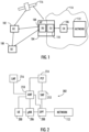
- Fig. 1 depicts examples of simplified system architectures only showing some elements and functional entities, all being logical units, whose implementation may differ from what is shown.
- the connections shown in Fig. 1 are logical connections; the actual physical connections may be different. It is apparent to a person skilled in the art that the system typically comprises also other functions and structures than those shown in Fig. 1 .
- Fig. 1 shows a part of an exemplifying radio access network.
- Fig. 1 shows devices 100 and 102.
- the devices 100 and 102 are configured to be in a wireless connection on one or more communication channels with a node 104.
- the node 104 is further connected to a core network 106.
- the node 104 may be an access node such as (e/g)NodeB serving devices in a cell.
- the node 104 may be a non-3GPP access node.
- the physical link from a device to a (e/g)NodeB is called uplink or reverse link and the physical link from the (e/g)NodeB to the device is called downlink or forward link.
- (e/g)NodeBs or their functionalities may be implemented by using any node, host, server or access point etc. entity suitable for such a usage.
- a communications system typically comprises more than one (e/g)NodeB in which case the (e/g)NodeBs may also be configured to communicate with one another over links, wired or wireless, designed for the purpose. These links may be used for signalling purposes.
- the (e/g)NodeB is a computing device configured to control the radio resources of communication system it is coupled to.
- the NodeB may also be referred to as a base station, an access point or any other type of interfacing device including a relay station capable of operating in a wireless environment.
- the (e/g)NodeB includes or is coupled to transceivers. From the transceivers of the (e/g)NodeB, a connection is provided to an antenna unit that establishes bi-directional radio links to devices.
- the antenna unit may comprise a plurality of antennas or antenna elements.
- the (e/g)NodeB is further connected to the core network 106 (CN or next generation core NGC). Depending on the deployed technology, the (e/g)NodeB is connected to a serving and packet data network gateway (S-GW +P-GW) or user plane function (UPF), for routing and forwarding user data packets and for providing connectivity of devices to one ore more external packet data networks, and to a mobile management entity (MME) or access mobility management function (AMF), for controlling access and mobility of the devices.
- S-GW +P-GW serving and packet data network gateway
- UPF user plane function
- MME mobile management entity
- AMF access mobility management function
- Exemplary embodiments of a device are a subscriber unit, a user device, a user equipment (UE), a user terminal, a terminal device, a mobile station, a mobile device, etc
- the device typically refers to a mobile or static device (e.g. a portable or non-portable computing device) that includes wireless mobile communication devices operating with or without an universal subscriber identification module (USIM), including, but not limited to, the following types of devices: mobile phone, smartphone, personal digital assistant (PDA), handset, device using a wireless modem (alarm or measurement device, etc.), laptop and/or touch screen computer, tablet, game console, notebook, and multimedia device.
- a device may also be a nearly exclusive uplink only device, of which an example is a camera or video camera loading images or video clips to a network.
- a device may also be a device having capability to operate in Internet of Things (IoT) network which is a scenario in which objects are provided with the ability to transfer data over a network without requiring human-to-human or human-to-computer interaction, e.g. to be used in smart power grids and connected vehicles.
- IoT Internet of Things
- the device may also utilise cloud.
- a device may comprise a user portable device with radio parts (such as a watch, earphones or eyeglasses) and the computation is carried out in the cloud.
- the device illustrates one type of an apparatus to which resources on the air interface are allocated and assigned, and thus any feature described herein with a device may be implemented with a corresponding apparatus, such as a relay node.
- a relay node is a layer 3 relay (self-backhauling relay) towards the base station.
- the device (or in some embodiments a layer 3 relay node) is configured to perform one or more of user equipment functionalities.
- CPS cyber-physical system
- ICT interconnected information and communications technology
- devices sensors, actuators, processors microcontrollers, etc.
- mobile cyber physical systems in which the physical system in question has inherent mobility, are a subcategory of cyber-physical systems. Examples of mobile physical systems include mobile robotics and electronics transported by humans or animals.
- apparatuses have been depicted as single entities, different units, processors and/or memory units (not all shown in Fig. 1 ) may be implemented.
- 5G enables using multiple input - multiple output (MIMO) antennas, many more base stations or nodes than the LTE (a so-called small cell concept), including macro sites operating in co-operation with smaller stations and employing a variety of radio technologies depending on service needs, use cases and/or spectrum available.
- 5G mobile communications supports a wide range of use cases and related applications including video streaming, augmented reality, different ways of data sharing and various forms of machine type applications (such as (massive) machine-type communications (mMTC), including vehicular safety, different sensors and real-time control.
- 5G is expected to have multiple radio interfaces, e.g. below 6GHz or above 24 GHz, cmWave and mmWave, and also being integrable with existing legacy radio access technologies, such as the LTE.
- Integration with the LTE may be implemented, at least in the early phase, as a system, where macro coverage is provided by the LTE and 5G radio interface access comes from small cells by aggregation to the LTE.
- 5G is planned to support both inter-RAT operability (such as LTE-5G) and inter-RI operability (inter-radio interface operability, such as below 6GHz - cmWave, 6 or above 24 GHz - cmWave and mmWave).
- inter-RAT operability such as LTE-5G
- inter-RI operability inter-radio interface operability, such as below 6GHz - cmWave, 6 or above 24 GHz - cmWave and mmWave.
- One of the concepts considered to be used in 5G networks is network slicing in which multiple independent and dedicated virtual sub-networks (network instances) may be created within the same infrastructure to run services that have different requirements on latency, reliability, throughput and mobility.
- the current architecture in LTE networks is fully distributed in the radio and fully centralized in the core network.
- the low latency applications and services in 5G require to bring the content close to the radio which leads to local break out and multi-access edge computing (MEC).
- MEC multi-access edge computing
- 5G enables analytics and knowledge generation to occur at the source of the data. This approach requires leveraging resources that may not be continuously connected to a network such as laptops, smartphones, tablets and sensors.
- MEC provides a distributed computing environment for application and service hosting. It also has the ability to store and process content in close proximity to cellular subscribers for faster response time.
- Edge computing covers a wide range of technologies such as wireless sensor networks, mobile data acquisition, mobile signature analysis, cooperative distributed peer-to-peer ad hoc networking and processing also classifiable as local cloud/fog computing and grid/mesh computing, dew computing, mobile edge computing, cloudlet, distributed data storage and retrieval, autonomic self-healing networks, remote cloud services, augmented and virtual reality, data caching, Internet of Things (massive connectivity and/or latency critical), critical communications (autonomous vehicles, traffic safety, real-time analytics, time-critical control, healthcare applications).
- the communication system is also able to communicate with other networks 112, such as a public switched telephone network, or a VoIP network, or the Internet, or a private network, or utilize services provided by them.
- the communication network may also be able to support the usage of cloud services, for example at least part of core network operations may be carried out as a cloud service (this is depicted in Fig. 1 by "cloud" 114).
- the communication system may also comprise a central control entity, or a like, providing facilities for networks of different operators to cooperate for example in spectrum sharing.
- Edge cloud may be brought into a radio access network (RAN) by utilizing network function virtualization (NFV) and software defined networking (SDN).
- RAN radio access network
- NFV network function virtualization
- SDN software defined networking
- Using the technology of edge cloud may mean access node operations to be carried out, at least partly, in a server, host or node operationally coupled to a remote radio head or base station comprising radio parts. It is also possible that node operations will be distributed among a plurality of servers, nodes or hosts.
- Application of cloudRAN architecture enables RAN real time functions being carried out at or close to a remote antenna site (in a distributed unit, DU 108) and non-real time functions being carried out in a centralized manner (in a centralized unit, CU 110).
- 5G may also utilize satellite communication to enhance or complement the coverage of 5G service, for example by providing backhauling.
- Possible use cases are providing service continuity for machine-to-machine (M2M) or Internet of Things (IoT) devices or for passengers on board of vehicles, Mobile Broadband, (MBB) or ensuring service availability for critical communications, and future railway/maritime/aeronautical communications.
- Satellite communication may utilise geostationary earth orbit (GEO) satellite systems, but also low earth orbit (LEO) satellite systems, in particular mega-constellations (systems in which hundreds of (nano)satellites are deployed).
- GEO geostationary earth orbit
- LEO low earth orbit
- mega-constellations systems in which hundreds of (nano)satellites are deployed.
- Each satellite in the mega-constellation may cover several satellite-enabled network entities that create on-ground cells.
- the on-ground cells may be created through an on-ground relay node or by a gNB located on-ground or in
- the depicted system is only an example of a part of a radio access system and in practice, the system may comprise a plurality of (e/g)NodeBs, the device may have an access to a plurality of radio cells and the system may comprise also other apparatuses, such as physical layer relay nodes or other network elements, etc. At least one of the (e/g)NodeBs or may be a Home(e/g)nodeB. Additionally, in a geographical area of a radio communication system a plurality of different kinds of radio cells as well as a plurality of radio cells may be provided.
- Radio cells may be macro cells (or umbrella cells) which are large cells, usually having a diameter of up to tens of kilometers, or smaller cells such as micro-, femto- or picocells.
- the (e/g)NodeBs of Fig. 1 may provide any kind of these cells.
- a cellular radio system may be implemented as a multilayer network including several kinds of cells. Typically, in multilayer networks, one access node provides one kind of a cell or cells, and thus a plurality of (e/g)NodeBs are required to provide such a network structure.
- a network which is able to use “plug-and-play" (e/g)Node Bs includes, in addition to Home (e/g)NodeBs (H(e/g)nodeBs), a home node B gateway, or HNB-GW (not shown in Fig. 1 ).
- HNB-GW HNB Gateway
- a HNB Gateway (HNB-GW) which is typically installed within an operator's network may aggregate traffic from a large number of HNBs back to a core network.
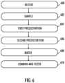
- Fig.2 illustrates an example of a communication system based on 5G network components.
- a terminal device, user terminal or user equipment 200 communicating via a 5G network 202 with a data network 112.
- the user terminal 200 is connected to a Radio Access Network RAN node, such as (e/g)NodeB 206 which provides the user terminal with a connection to the network 112 via one or more User Plane Functions, UPF 208.
- the user terminal 200 is further connected to Core Access and Mobility Management Function, AMF 210, which is a control plane core connector for (radio) access network and can be seen from this perspective as the 5G version of Mobility Management Entity, MME, in LTE.
- AMF 210 Core Access and Mobility Management Function
- the 5G network further comprises Session Management Function, SMF 212, which is responsible for subscriber sessions, such as session establishment, modify and release, and a Policy Control Function, PCF 214 which is configured to govern network behavior by providing policy rules to control plane functions.
- SMF 212 Session Management Function
- PCF 214 Policy Control Function
- the 5G network may further comprise a location management function, LMF 216, which may be configured to determine the location of the terminal device 200 based on information received from the terminal device and/or gNB 206.
- the trend in transmitter design is to utilise wide bandwidth transmitters because they may offer savings in costs as the number of transmitters may be reduced.
- Base stations with wide bandwidth support are capable of transmitting on one or more transmission bands at the same time.
- a random carrier configuration may be assigned to the base station.
- Figs. 3A, 3B and 3C illustrate examples of some common signal configurations for Dual, Triple and Quad Band cases where the base station supports all the bands with a single power amplifier, PA. For simplicity, only a single carrier is shown per band. However, the problem or the solution described here in will not change if multiple carriers were assigned per each band
- Fig. 3A illustrates a dual band example.
- Two bands X1 300 and X2 302 are used.
- Intermodulations, IMs, due to low order non-linear cross terms 308, 310 (or some low order special terms) occur near the signals.
- IMs due to low order non-linear cross terms 308, 310 (or some low order special terms) occur near the signals.
- a power amplifier model supporting these terms will not alias as they are within the Nyquist bandwidth defined within -fs/2 to fs/2, where fs the sampling rate of the signal.
- third order terms may not alias.
- Third, fifth, seventh and the rest of higher order intermodulations 304, 306 are outside of -fs/2 and fs/2 and they alias. It may be noted that these alias terms may include high order dual and high order special terms as well.
- Fig. 3B illustrates a triple band example.
- Three bands X1 300, X2 302 and X3 320 are used.
- Intermodulations, IMs, due to low order non-linear cross terms 308, 310, 322 (or some low order special terms) occur near the signals.
- Fig. 3C illustrates a quad band example.
- Four bands X1 300, X2 302, X3 320 and X4 326 are used.
- Intermodulations, IMs, due to low order non-linear cross terms 308, 310, 322, 326, 328 (or some low order special terms) occur near the signals.
- the predistortion is more difficult to realise than in a narrow bandwidth transmitter.
- the solution to predistortion problem requires allocating increased hardware resources for the Digital Pre-Distortion, DPD, algorithm.
- DPD Digital Pre-Distortion
- ASICs consist of fixed hardware allocations for DPD.
- FPGA Field Programmable Gate Array
- Fig. 4 illustrates an example of a transmission chain.
- the example shows a power amplifier 400, PA, and a digital predistortion circuit 402.
- the transmission chain may be a part of a base station, eNB, or gNB transceiver, or any other transceiver or transmitter.
- the transmission chain receives as an input a signal 404 sampled by a sampler 405 at a given sample frequency fs, the signal comprising a linear vector, composite non-linear terms causing intermodulation outside Nyquist band within -fs/2 to fs/2 of the input signal and further non-linear terms causing intermodulation inside the Nyquist band;
- the digital predistortion circuit 402 applies a predistortion PreD(n) to the input signal.
- the predistortion is the inverse of the power amplifier model of the PA 400.
- the pre-distorted signal 406 is taken to the PA which amplifies the signal to generate amplified signal 408.
- Power amplifier intermodulation terms are related to the pre-distortion process such that the intermodulation terms given in the PA model are rotated 180 degrees (reversal of the sign).
- Nonlinear vector coefficients in Eqs. 1 and 2 can be close with relation to their magnitudes. It may be further noted that the IM component ( NL ) of Eq. 2 has inverse sign compared to the PA model in Eq. 1.
- NL ⁇ NL term 1 + NL term 2 + NL term 3 + NL term
- NL term x n x n 2 n composite non linear term
- NL term x 1 n x 1 n 2
- NL term 3 x 1 n x 2 n 2
- Extra terms x 1 n x 3 n 2 , x 1 n x 4 n 2 x 1( n )( Conj ( x3 ( n )) 2 ,x 1( n )( Conj ( x4 ( n )) 2 ,conj ( x 1( n ))
- Figs. 3A, 3B and 3C illustrate, these IM components generated from the PA model consist of a wider frequency span causing them to place beyond the Nyquist frequency (-fs/2 to fs/2). Hence, aliasing would occur for those terms.
- a traditional solution is to oversample the input signal x ( n ) and its components x 1( n ), and x 2( n ) to a high sample rate before computing the non-linear terms.
- this is problematic from hardware realisation point of view. It is not without consequences, as doubling of the sampling rate will double the used hardware gates in an FPGA or an ASIC environment.
- oversampling When oversampling is utilised, the input signal is oversampled by a factor of two, three or four as long as IM products don't alias.
- IM products don't alias.
- In the first oversampling method zeros are inserted between samples followed up with lowpass filtering. Oversampling of two requires single zeros to be inserted.
- an additional phase i.e. x(n - 0.5)
- additional phases x ( n - 0.25), x ( n - 0.5) and x ( n - 0.75) may be created to oversample by 4.
- f denotes a fractional delay filter, having a filter response which induces a group delay of 0.5 samples. Thus, it generates half a sample shift to x ( n ).
- the mentioned preferred HW based oversampling by 2 maintains two signal phases x 0 ( n ), and x 1 ( n ) . These samples have an offset of 0.5 samples with relation to each other. Individually, each of the phases are sampled at fs where collectively, when interleaved as in (Eq.11), both phases as in x up ( n ) achive an effective sample rate of 2*fs.
- HW based oversampling does not require HW gates to clock at a higher rate (2*fs, for example) to achieve an oversampled signal.
- This technique when achieving an oversampling ratio of two, may be denoted as dual data rate, DDR.
- DDR dual data rate
- QDR Quad Data Rate
- a sampling ratio of one may be denoted as single data rate, SDR.
- PreD L ⁇ ⁇ x 0 n ⁇ ⁇ D ⁇ ⁇ NL 0 ⁇
- [ NL 0 ] is the non-linear SDR vector having a form:
- [ NL 0 ] [ NL term 10 NL term 20 NL term 30 NL term 40 NL term 50 ] and D is the DPD coefficient vector.
- a DDR implementation of the pre-distortion signal may require HW resources that the ASIC or FPGA may not have.
- Other possibility is to reduce the terms to match the available HW resources within the ASIC or the FPGA. Thus, a degradation is expected in that instance.
- FIG. 5 illustrates an example of an apparatus which is one possible realisation of Eq.16.
- the input may be a signal 404 sampled at a given sample frequency fs.
- the apparatus of Fig. 5 comprises a composite single band DDR block 500 and an N band DDR block 502.
- Eq. 16 comprises an [ NL 0 ] term comprises both composite and multi-band terms. It may be noted that the term multi-band terms is used to represent both cross and special terms.
- Eq. 16 further comprises an [ NL 1 ] term (corresponding to DDR Phase 1).
- the non-linear element 506 after oversampler 504 within the DPD block 500 processes the composite terms of phase 0 and phase 1.
- the output of the non-linear element 506 is then decimated in 508.
- the non-linear element 514 after the band splitter 510 and oversampling 512 processes multi-band terms of phase 0 and phase 1.
- the signal is decimated 516 before supplying it to the summing element 518 where the outputs of blocks 500 and 502 are combined before filtering 520, and pre-distortion signal 522 at SDR rate is obtained.
- decimation composite terms and multi band terms are both operated at DDR.
- the blocks 500, 502 would require four times as many non-linear elements. Since ASICs or FGPAs have fixed hardware resources, the realisations of Eq.16 may not be able achieve the DPD complexity needed to meet emission requirements.
- the flowchart of Fig. 6 illustrates an example embodiment.
- the flowchart illustrates an example of the operation of an apparatus or entity configured to perform predistortion of a signal forwarded to a power amplifier.
- the apparatus is configured receive as an input a signal comprising at least two signal components, each signal component being received on a different frequency band.
- the apparatus is configured to sample the input signal at a given sample frequency fs, the signal comprising linear terms, composite non-linear terms causing intermodulation outside Nyquist band of ⁇ fs/2 of the input signal and further non-linear terms causing intermodulation inside the Nyquist band, the further non-linear terms comprising multi-band terms.
- the apparatus is configured to apply oversampling by a given factor to the input signal in a first predistortion circuit for processing the linear terms and composite non-linear terms causing intermodulation outside Nyquist band.
- the factor may be dual triple or quad, for example.
- the apparatus is configured to process the input signal without oversampling in a second predistortion circuit in parallel with the first predistortion circuit for the further non-linear terms causing intermodulation inside the Nyquist band.
- step 608 the apparatus is configured to match the rates of the output signals of the first and second predistortion circuits.
- the apparatus is configured to combine and filter the output signals of the first and second predistortion circuits to obtain a pre-distorted signal for a power amplifier.
- the proposed solution of Fig. 6 preserves the HW resources by reducing the number of oversampled operations done, compared to the solution of Fig.5 , for example.
- the prior art solution of Fig. 5 requires using DDR rate for all non-linear terms including NL term 2 , NL term 3 , NL term 4 , and NL term 5 .
- All other special terms such as NL term 2 , NL term , NL term , and NL term can be operated at SDR rates.
- the hardware blocks that are save by applying the solution of Eq. 17 may be used to introduce new special (cross terms).
- cross terms an improvement in the DPD performance relative to the typical DDR solution is achieved.
- additional cross terms can be added for improved performance.
- Typical savings and the corresponding addition of new terms in practical transceivers can be as high as 20 HW resource blocks.
- Figure 7 illustrates an example of an apparatus which is one possible realisation of Eq.17.
- the input may be a signal 404 sampled at a given sample frequency fs.
- the apparatus of Fig. 7 comprises a first predistortion circuit or a composite single band DDR block 700 and a second predistortion circuit or an N band SDR block 702 which operate in parallel.
- Eq. 17 comprises an [ NL 10 ] term (corresponding to DDR Phase 0) and an [ NL 11 ] term (corresponding to DDR Phase 1), and these are realised with non-linear element 706 within the first predistortion DDR circuit 700 after the oversampler 704.
- the [ NL SDR ] terms of Eq.17 are realized non-linear element 712 after the band splitter 708 within the second predistortion SDR circuit 502.
- the oversampling block 714 may be realised with the second oversampling method mentioned above, where phase 0 signal is used to generate a phase 1 signal with the help of a fractional delay filter (such as f ( C 2 ⁇ NL SDR ) . Collectively both phases achieve a DDR rate.
- the SDR terms from second predistortion circuit 702 are oversampled 714 so that they can be summed 716 with the DDR terms from the first predistortion circuit 700. Finally, the signal is filtered to obtain pre-distortion signal 720 at DDR rate. Before the summation 716, both linear, composite, and special (cross) terms are rate matched to DDR.
- a SDR rate i.e, both linear, composite, and special (cross) terms are rate matched to SDR.
- the predistortion circuit 700 comprises a decimator 800.
- the cross terms in predistortion circuit 702 output an SDR signal.
- the linear and composite terms (NL_term1) are still operating at DDR rates.
- the DDR signal will be filtered and decimated to produce a SDR rate.
- the decimation operations 800 can be implemented in two ways. First, the IMs could alias are filtered and decimated. This generates a SDR phase 0 signal. Second, a polyphase filtering approach may be applied. There both phases are used to produce an output phase of 0 or 1. Generating merely an output phase 0 is equivalent to the first decimation process.
- PreD SDR decimate f L 0 ⁇ ⁇ x 0 n ⁇ + L 1 ⁇ ⁇ x 1 n ⁇ + C 0 ⁇ ⁇ NL term 10 + C 1 ⁇ ⁇ NL term 11 + C 3 ⁇ ⁇ NL SDR ⁇
- L 0 , L 1 , C 0 , C 1 , C 3 , .. are coefficient vectors. Other terms are the same as in Eq.17.
- the DPD coefficients may be computed in various ways. For example, iterative algorithms or a Least Squares methodology may be applied. Solution can be DDR based or DDR/SDR based (subsampled solver). One skilled in the art is aware of these methods.
- Figs. 9A and 9B illustrate an example embodiment.
- the figures illustrate a simplified example of an apparatuses applying example embodiments of the invention.
- apparatuses are depicted herein as an example illustrating some embodiments. It is apparent to a person skilled in the art that the apparatuses may also comprise other functions and/or structures and not all described functions and structures are required. Although the apparatuses has been depicted as one entity, different modules and memory may be implemented in one or more physical or logical entities.
- Fig. 9A illustrates an apparatus or network element applying example embodiments of the invention.
- the apparatus may be a network element or a part of a network element.
- the apparatus may comprise several network entities connected to each other.
- the apparatus may be a base station or a part of a base station or a gNB or a part of a gNB.
- the apparatus 900 of the example includes a control circuitry 900 configured to control at least part of the operation of the apparatus.
- the apparatus may comprise a memory 902 for storing data. Furthermore, the memory may store software 904 executable by the control circuitry 900. The memory may be integrated in the control circuitry.
- the apparatus further comprises one or more interface circuitries 906, 908 configured to connect the apparatus to other devices and to network elements of the radio access network.
- the interface 906 may provide a wired or wireless connection.
- the interface may provide a connection to other similar network elements or core network.
- the interface 908 may provide a wireless connection for example to terminal devices or UEs.
- the interface may comprise a transmitter or a transceiver with a power amplifier and a predistortion circuit.
- the software 904 may comprise a computer program comprising program code means adapted to cause the control circuitry 900 of the apparatus to control the apparatus to realise at least some of the example embodiments described above.
- the apparatus of Fig. 9A of may be shared between two physically separate devices, forming one operational entity. Therefore, the apparatus may be seen to depict the operational entity comprising one or more physically separate devices for executing at least some of the described processes.
- the apparatus of Fig. 9B may comprise a remote control unit RCU 930, such as a host computer or a server computer, operatively coupled (e.g. via a wireless or wired network) to a remote distributed unit RDU 932 located in the base station.
- RCU 930 such as a host computer or a server computer
- the execution of at least some of the described processes may be shared among the RDU 932 and the RCU 930.
- the RCU 930 may generate a virtual network through which the RCU 930 communicates with the RDU 932.
- virtual networking may involve a process of combining hardware and software network resources and network functionality into a single, software-based administrative entity, a virtual network.
- Network virtualization may involve platform virtualization, often combined with resource virtualization.
- Network virtualization may be categorized as external virtual networking which combines many networks, or parts of networks, into the server computer or the host computer (e.g. to the RCU). External network virtualization is targeted to optimized network sharing. Another category is internal virtual networking which provides network-like functionality to the software containers on a single system. Virtual networking may also be used for testing the terminal device.
- the virtual network may provide flexible distribution of operations between the RDU and the RCU.
- any digital signal processing task may be performed in either the RDU or the RCU and the boundary where the responsibility is shifted between the RDU and the RCU may be selected according to implementation.
- the apparatuses or controllers able to perform the above-described steps may be implemented as an electronic digital computer, processing system or a circuitry which may comprise a working memory (random access memory, RAM), a central processing unit (CPU), and a system clock.
- the CPU may comprise a set of registers, an arithmetic logic unit, and a controller.
- the processing system, controller or the circuitry is controlled by a sequence of program instructions transferred to the CPU from the RAM.
- the controller may contain a number of microinstructions for basic operations. The implementation of microinstructions may vary depending on the CPU design.
- the program instructions may be coded by a programming language, which may be a high-level programming language, such as C, Java, etc., or a low-level programming language, such as a machine language, or an assembler.
- the electronic digital computer may also have an operating system, which may provide system services to a computer program written with the program instructions.
- circuitry refers to all of the following: (a) hardware-only circuit implementations, such as implementations in only analog and/or digital circuitry, and (b) combinations of circuits and software (and/or firmware), such as (as applicable): (i) a combination of processor(s) or (ii) portions of processor(s)/software including digital signal processor(s), software, and memory(ies) that work together to cause an apparatus to perform various functions, and (c) circuits, such as a microprocessor(s) or a portion of a microprocessor(s), that require software or firmware for operation, even if the software or firmware is not physically present.
- circuitry' applies to all uses of this term in this application.
- the term 'circuitry' would also cover an implementation of merely a processor (or multiple processors) or a portion of a processor and its (or their) accompanying software and/or firmware.
- the term 'circuitry' would also cover, for example and if applicable to the particular element, a baseband integrated circuit or applications processor integrated circuit for a mobile phone or a similar integrated circuit in a server, a cellular network device, or another network device.
- An embodiment provides a computer program embodied on a distribution medium, comprising program instructions which, when loaded into an electronic apparatus, are configured to control the apparatus to execute the embodiments described above.
- the computer program may be in source code form, object code form, or in some intermediate form, and it may be stored in some sort of carrier, which may be any entity or device capable of carrying the program.
- carrier include a record medium, computer memory, read-only memory, and a software distribution package, for example.
- the computer program may be executed in a single electronic digital computer or it may be distributed amongst a number of computers.
- the apparatus may also be implemented as one or more integrated circuits, such as application-specific integrated circuits, ASIC.
- Other hardware embodiments are also feasible, such as a circuit built of separate logic components.
- a hybrid of these different implementations is also feasible.
Landscapes
- Engineering & Computer Science (AREA)
- Physics & Mathematics (AREA)
- Power Engineering (AREA)
- Computer Networks & Wireless Communication (AREA)
- Nonlinear Science (AREA)
- Signal Processing (AREA)
- Algebra (AREA)
- General Physics & Mathematics (AREA)
- Mathematical Analysis (AREA)
- Mathematical Optimization (AREA)
- Pure & Applied Mathematics (AREA)
- Microelectronics & Electronic Packaging (AREA)
- Spectroscopy & Molecular Physics (AREA)
- Transmitters (AREA)
- Amplifiers (AREA)
Abstract
Description
- The exemplary and non-limiting embodiments of the invention relate generally to wireless communication systems. The exemplary and non-limiting embodiments of the invention relate especially to apparatuses and methods in wireless communication networks.
- In transmitters, for example base station transmitters used in wireless communication systems the trend is to use wide bandwidth transmitters which have the capability of transmitting utilising multiple Radio Frequency (RF) bands. Wide band radios are efficient allowing deploying a single base station as opposed to dedicating a separate base station for each band.
- In transmitters, for example base station transmitters used in wireless communication systems, a power amplifier is used to amplify the signal to be transmitted to the required power level. Usually, power amplifiers are driven into compression for increasing the efficiency of the amplifier. This causes the distortion in the output signal of the amplifier. This distortion may be compensated by a digital predistortion. Using a wide bandwidth in transmission causes some problems in the realisation of predistortion.
- The following presents a simplified summary of the invention in order to provide a basic understanding of some aspects of the invention. This summary is not an extensive overview of the invention. It is not intended to identify key/critical elements of the invention or to delineate the scope of the invention. Its sole purpose is to present some concepts of the invention in a simplified form as a prelude to a more detailed description that is presented later.
- According to an aspect of the present invention, there is provided an apparatus, comprising: at least one processor; and at least one memory including computer program code, the at least one memory and the computer program code configured to, with the at least one processor, cause the apparatus at least to perform: receive as an input a signal comprising at least two signal components, each signal component being received on a different frequency band; sample the input signal at a given sample frequency fs, the signal comprising linear terms, composite non-linear terms causing intermodulation outside Nyquist band of ± fs/2 of the input signal and further non-linear terms causing intermodulation inside the Nyquist band, the further non-linear terms comprising multi-band terms; apply oversampling by a given factor to the input signal in a first predistortion circuit for processing the linear terms and composite non-linear terms causing intermodulation outside Nyquist band; process the input signal without oversampling in a second predistortion circuit in parallel with the first predistortion circuit for the further non-linear terms causing intermodulation inside the Nyquist band; match the rates of the output signals of the first and second predistortion circuits; combine and filter the output signals of the first and second predistortion circuits to obtain a pre-distorted signal for a power amplifier.
- According to an aspect of the present invention, there is provided a method comprising: receiving as an input a signal comprising at least two signal components, each signal component being received on a different frequency band; sampling the input signal at a given sample frequency fs, the signal comprising linear terms, composite non-linear terms causing intermodulation outside Nyquist band of ± fs/2 of the input signal and further non-linear terms causing intermodulation inside the Nyquist band, the further non-linear terms comprising multi-band terms; applying oversampling by a given factor to the input signal in a first predistortion circuit for processing the linear terms and composite non-linear terms causing intermodulation outside Nyquist band; processing the input signal without oversampling in a second predistortion circuit in parallel with the first predistortion circuit for the further non-linear terms causing intermodulation inside the Nyquist band; matching the rates of the output signals of the first and second predistortion circuits; combining and filtering the output signals of the first and second predistortion circuits to obtain a pre-distorted signal for a power amplifier.
- According to an aspect of the present invention, there is provided a computer program comprising instructions for causing an apparatus to perform at least the following: receiving as an input a signal comprising at least two signal components, each signal component being received on a different frequency band; sampling the input signal at a given sample frequency fs, the signal comprising linear terms, composite non-linear terms causing intermodulation outside Nyquist band of ± fs/2 of the input signal and further non-linear terms causing intermodulation inside the Nyquist band, the further non-linear terms comprising multi-band terms; applying oversampling by a given factor to the input signal in a first predistortion circuit for processing the linear terms and composite non-linear terms causing intermodulation outside Nyquist band; processing the input signal without oversampling in a second predistortion circuit in parallel with the first predistortion circuit for the further non-linear terms causing intermodulation inside the Nyquist band; matching the rates of the output signals of the first and second predistortion circuits; combining and filtering the output signals of the first and second predistortion circuits to obtain a pre-distorted signal for a power amplifier.
- An embodiment provides an apparatus comprising means for receiving as an input a signal comprising at least two signal components, each signal component being received on a different frequency band; means for sampling the input signal at a given sample frequency fs, the signal comprising linear terms, composite non-linear terms causing intermodulation outside Nyquist band of ± fs/2 of the input signal and further non-linear terms causing intermodulation inside the Nyquist band, the further non-linear terms comprising multi-band terms; means for applying oversampling by a given factor to the input signal in a first predistortion circuit for processing the linear terms and composite non-linear terms causing intermodulation outside Nyquist band; means for processing the input signal without oversampling in a second predistortion circuit in parallel with the first predistortion circuit for the further non-linear terms causing intermodulation inside the Nyquist band; means for matching the rates of the output signals of the first and second predistortion circuits; means for combining and filtering the output signals of the first and second predistortion circuits to obtain a pre-distorted signal for a power amplifier.
- An embodiment provides a non-transitory computer program embodied on a distribution medium, comprising program instructions which, when loaded into an electronic apparatus, are configured to control the apparatus to execute at least the following: receiving as an input a signal comprising at least two signal components, each signal component being received on a different frequency band; sampling the input signal at a given sample frequency fs, the signal comprising linear terms, composite non-linear terms causing intermodulation outside Nyquist band of ± fs/2 of the input signal and further non-linear terms causing intermodulation inside the Nyquist band, the further non-linear terms comprising multi-band terms; applying oversampling by a given factor to the input signal in a first predistortion circuit for processing the linear terms and composite non-linear terms causing intermodulation outside Nyquist band; processing the input signal without oversampling in a second predistortion circuit in parallel with the first predistortion circuit for the further non-linear terms causing intermodulation inside the Nyquist band; matching the rates of the output signals of the first and second predistortion circuits; combining and filtering the output signals of the first and second predistortion circuits to obtain a pre-distorted signal for a power amplifier.
- One or more examples of implementations are set forth in more detail in the accompanying drawings and the description below. Other features will be apparent from the description and drawings, and from the claims. The embodiments and/or examples and features, if any, described in this specification that do not fall under the scope of the independent claims are to be interpreted as examples useful for understanding various embodiments of the invention.
- Example embodiments of the present invention are described below, by way of example only, with reference to the accompanying drawings, in which
-
Figures 1 and 2 illustrate examples of simplified system architecture of communication systems; -
Figures 3A, 3B and3C illustrate examples of some common signal configurations; -
Figure 4 illustrates an example of a transmission chain; -
Figure 5 illustrates an example of a prior art apparatus; -
Figure 6 is a flowchart illustrating an embodiment of the invention; -
Figures 7 and 8 illustrates examples of apparatus of some example embodiments; and -
Figures 9A and 9B illustrate simplified examples of apparatuses applying some example embodiments of the invention. - The following embodiments are only examples. Although the specification may refer to "an", "one", or "some" embodiment(s) in several locations, this does not necessarily mean that each such reference is to the same embodiment(s), or that the feature only applies to a single embodiment. Single features of different example embodiments may also be combined to provide other embodiments. Furthermore, words "comprising" and "including" should be understood as not limiting the described embodiments to consist of only those features that have been mentioned and such embodiments may also contain features, structures, units, modules etc. that have not been specifically mentioned.
- Some example embodiments of the present invention are applicable to a user terminal, a communication device, a base station, eNodeB, gNodeB, a distributed realisation of a base station, a network element of a communication system, a corresponding component, and/or to any communication system or any combination of different communication systems that support required functionality.
- The protocols used, the specifications of communication systems, servers and user equipment, especially in wireless communication, develop rapidly. Such development may require extra changes to an embodiment. Therefore, all words and expressions should be interpreted broadly and they are intended to illustrate, not to restrict, embodiments.
- In the following, different exemplifying embodiments will be described using, as an example of an access architecture to which the embodiments may be applied, a radio access architecture based on long term evolution advanced (LTE Advanced, LTE-A) or new radio (NR, 5G), without restricting the embodiments to such an architecture, however. The embodiments may also be applied to other kinds of communications networks having suitable means by adjusting parameters and procedures appropriately. Some examples of other options for suitable systems are the universal mobile telecommunications system (UMTS) radio access network (UTRAN), wireless local area network (WLAN or WiFi), worldwide interoperability for microwave access (WiMAX), Bluetooth®, personal communications services (PCS), ZigBee®, wideband code division multiple access (WCDMA), systems using ultra-wideband (UWB) technology, sensor networks, mobile ad-hoc networks (MANETs) and Internet Protocol multimedia subsystems (IMS) or any combination thereof.
-
Fig. 1 depicts examples of simplified system architectures only showing some elements and functional entities, all being logical units, whose implementation may differ from what is shown. The connections shown inFig. 1 are logical connections; the actual physical connections may be different. It is apparent to a person skilled in the art that the system typically comprises also other functions and structures than those shown inFig. 1 . - The example embodiments are not, however, restricted to the system given as an example but a person skilled in the art may apply the solution to other communication systems provided with necessary properties.
- The example of
Fig. 1 shows a part of an exemplifying radio access network. -
Fig. 1 showsdevices devices node 104. Thenode 104 is further connected to acore network 106. In one example, thenode 104 may be an access node such as (e/g)NodeB serving devices in a cell. In one example, thenode 104 may be a non-3GPP access node. The physical link from a device to a (e/g)NodeB is called uplink or reverse link and the physical link from the (e/g)NodeB to the device is called downlink or forward link. It should be appreciated that (e/g)NodeBs or their functionalities may be implemented by using any node, host, server or access point etc. entity suitable for such a usage. - A communications system typically comprises more than one (e/g)NodeB in which case the (e/g)NodeBs may also be configured to communicate with one another over links, wired or wireless, designed for the purpose. These links may be used for signalling purposes. The (e/g)NodeB is a computing device configured to control the radio resources of communication system it is coupled to. The NodeB may also be referred to as a base station, an access point or any other type of interfacing device including a relay station capable of operating in a wireless environment. The (e/g)NodeB includes or is coupled to transceivers. From the transceivers of the (e/g)NodeB, a connection is provided to an antenna unit that establishes bi-directional radio links to devices. The antenna unit may comprise a plurality of antennas or antenna elements. The (e/g)NodeB is further connected to the core network 106 (CN or next generation core NGC). Depending on the deployed technology, the (e/g)NodeB is connected to a serving and packet data network gateway (S-GW +P-GW) or user plane function (UPF), for routing and forwarding user data packets and for providing connectivity of devices to one ore more external packet data networks, and to a mobile management entity (MME) or access mobility management function (AMF), for controlling access and mobility of the devices.
- Exemplary embodiments of a device are a subscriber unit, a user device, a user equipment (UE), a user terminal, a terminal device, a mobile station, a mobile device, etc
- The device typically refers to a mobile or static device ( e.g. a portable or non-portable computing device) that includes wireless mobile communication devices operating with or without an universal subscriber identification module (USIM), including, but not limited to, the following types of devices: mobile phone, smartphone, personal digital assistant (PDA), handset, device using a wireless modem (alarm or measurement device, etc.), laptop and/or touch screen computer, tablet, game console, notebook, and multimedia device. It should be appreciated that a device may also be a nearly exclusive uplink only device, of which an example is a camera or video camera loading images or video clips to a network. A device may also be a device having capability to operate in Internet of Things (IoT) network which is a scenario in which objects are provided with the ability to transfer data over a network without requiring human-to-human or human-to-computer interaction, e.g. to be used in smart power grids and connected vehicles. The device may also utilise cloud. In some applications, a device may comprise a user portable device with radio parts (such as a watch, earphones or eyeglasses) and the computation is carried out in the cloud.
- The device illustrates one type of an apparatus to which resources on the air interface are allocated and assigned, and thus any feature described herein with a device may be implemented with a corresponding apparatus, such as a relay node. An example of such a relay node is a layer 3 relay (self-backhauling relay) towards the base station. The device (or in some embodiments a layer 3 relay node) is configured to perform one or more of user equipment functionalities.
- Various techniques described herein may also be applied to a cyber-physical system (CPS) (a system of collaborating computational elements controlling physical entities). CPS may enable the implementation and exploitation of massive amounts of interconnected information and communications technology, ICT, devices (sensors, actuators, processors microcontrollers, etc.) embedded in physical objects at different locations. Mobile cyber physical systems, in which the physical system in question has inherent mobility, are a subcategory of cyber-physical systems. Examples of mobile physical systems include mobile robotics and electronics transported by humans or animals.
- Additionally, although the apparatuses have been depicted as single entities, different units, processors and/or memory units (not all shown in
Fig. 1 ) may be implemented. - 5G enables using multiple input - multiple output (MIMO) antennas, many more base stations or nodes than the LTE (a so-called small cell concept), including macro sites operating in co-operation with smaller stations and employing a variety of radio technologies depending on service needs, use cases and/or spectrum available. 5G mobile communications supports a wide range of use cases and related applications including video streaming, augmented reality, different ways of data sharing and various forms of machine type applications (such as (massive) machine-type communications (mMTC), including vehicular safety, different sensors and real-time control. 5G is expected to have multiple radio interfaces, e.g. below 6GHz or above 24 GHz, cmWave and mmWave, and also being integrable with existing legacy radio access technologies, such as the LTE. Integration with the LTE may be implemented, at least in the early phase, as a system, where macro coverage is provided by the LTE and 5G radio interface access comes from small cells by aggregation to the LTE. In other words, 5G is planned to support both inter-RAT operability (such as LTE-5G) and inter-RI operability (inter-radio interface operability, such as below 6GHz - cmWave, 6 or above 24 GHz - cmWave and mmWave). One of the concepts considered to be used in 5G networks is network slicing in which multiple independent and dedicated virtual sub-networks (network instances) may be created within the same infrastructure to run services that have different requirements on latency, reliability, throughput and mobility.
- The current architecture in LTE networks is fully distributed in the radio and fully centralized in the core network. The low latency applications and services in 5G require to bring the content close to the radio which leads to local break out and multi-access edge computing (MEC). 5G enables analytics and knowledge generation to occur at the source of the data. This approach requires leveraging resources that may not be continuously connected to a network such as laptops, smartphones, tablets and sensors. MEC provides a distributed computing environment for application and service hosting. It also has the ability to store and process content in close proximity to cellular subscribers for faster response time. Edge computing covers a wide range of technologies such as wireless sensor networks, mobile data acquisition, mobile signature analysis, cooperative distributed peer-to-peer ad hoc networking and processing also classifiable as local cloud/fog computing and grid/mesh computing, dew computing, mobile edge computing, cloudlet, distributed data storage and retrieval, autonomic self-healing networks, remote cloud services, augmented and virtual reality, data caching, Internet of Things (massive connectivity and/or latency critical), critical communications (autonomous vehicles, traffic safety, real-time analytics, time-critical control, healthcare applications).
- The communication system is also able to communicate with
other networks 112, such as a public switched telephone network, or a VoIP network, or the Internet, or a private network, or utilize services provided by them. The communication network may also be able to support the usage of cloud services, for example at least part of core network operations may be carried out as a cloud service (this is depicted inFig. 1 by "cloud" 114). The communication system may also comprise a central control entity, or a like, providing facilities for networks of different operators to cooperate for example in spectrum sharing. - The technology of Edge cloud may be brought into a radio access network (RAN) by utilizing network function virtualization (NFV) and software defined networking (SDN). Using the technology of edge cloud may mean access node operations to be carried out, at least partly, in a server, host or node operationally coupled to a remote radio head or base station comprising radio parts. It is also possible that node operations will be distributed among a plurality of servers, nodes or hosts. Application of cloudRAN architecture enables RAN real time functions being carried out at or close to a remote antenna site (in a distributed unit, DU 108) and non-real time functions being carried out in a centralized manner (in a centralized unit, CU 110).
- It should also be understood that the distribution of labour between core network operations and base station operations may differ from that of the LTE or even be non-existent. Some other technology advancements probably to be used are Big Data and all-IP, which may change the way networks are being constructed and managed. 5G (or new radio, NR) networks are being designed to support multiple hierarchies, where MEC servers can be placed between the core and the base station or nodeB (gNB). It should be appreciated that MEC can be applied in 4G networks as well.
- 5G may also utilize satellite communication to enhance or complement the coverage of 5G service, for example by providing backhauling. Possible use cases are providing service continuity for machine-to-machine (M2M) or Internet of Things (IoT) devices or for passengers on board of vehicles, Mobile Broadband, (MBB) or ensuring service availability for critical communications, and future railway/maritime/aeronautical communications. Satellite communication may utilise geostationary earth orbit (GEO) satellite systems, but also low earth orbit (LEO) satellite systems, in particular mega-constellations (systems in which hundreds of (nano)satellites are deployed). Each satellite in the mega-constellation may cover several satellite-enabled network entities that create on-ground cells. The on-ground cells may be created through an on-ground relay node or by a gNB located on-ground or in a satellite.
- It is obvious for a person skilled in the art that the depicted system is only an example of a part of a radio access system and in practice, the system may comprise a plurality of (e/g)NodeBs, the device may have an access to a plurality of radio cells and the system may comprise also other apparatuses, such as physical layer relay nodes or other network elements, etc. At least one of the (e/g)NodeBs or may be a Home(e/g)nodeB. Additionally, in a geographical area of a radio communication system a plurality of different kinds of radio cells as well as a plurality of radio cells may be provided. Radio cells may be macro cells (or umbrella cells) which are large cells, usually having a diameter of up to tens of kilometers, or smaller cells such as micro-, femto- or picocells. The (e/g)NodeBs of
Fig. 1 may provide any kind of these cells. A cellular radio system may be implemented as a multilayer network including several kinds of cells. Typically, in multilayer networks, one access node provides one kind of a cell or cells, and thus a plurality of (e/g)NodeBs are required to provide such a network structure. - For fulfilling the need for improving the deployment and performance of communication systems, the concept of "plug-and-play" (e/g)NodeBs has been introduced. Typically, a network which is able to use "plug-and-play" (e/g)Node Bs, includes, in addition to Home (e/g)NodeBs (H(e/g)nodeBs), a home node B gateway, or HNB-GW (not shown in
Fig. 1 ). A HNB Gateway (HNB-GW), which is typically installed within an operator's network may aggregate traffic from a large number of HNBs back to a core network. -
Fig.2 illustrates an example of a communication system based on 5G network components. A terminal device, user terminal oruser equipment 200 communicating via a5G network 202 with adata network 112. Theuser terminal 200 is connected to a Radio Access Network RAN node, such as (e/g)NodeB 206 which provides the user terminal with a connection to thenetwork 112 via one or more User Plane Functions,UPF 208. Theuser terminal 200 is further connected to Core Access and Mobility Management Function,AMF 210, which is a control plane core connector for (radio) access network and can be seen from this perspective as the 5G version of Mobility Management Entity, MME, in LTE. The 5G network further comprises Session Management Function,SMF 212, which is responsible for subscriber sessions, such as session establishment, modify and release, and a Policy Control Function,PCF 214 which is configured to govern network behavior by providing policy rules to control plane functions. The 5G network may further comprise a location management function,LMF 216, which may be configured to determine the location of theterminal device 200 based on information received from the terminal device and/orgNB 206. - As mentioned, the trend in transmitter design is to utilise wide bandwidth transmitters because they may offer savings in costs as the number of transmitters may be reduced.
- Base stations with wide bandwidth support are capable of transmitting on one or more transmission bands at the same time. In each of the bands, a random carrier configuration may be assigned to the base station.
Figs. 3A, 3B and3C illustrate examples of some common signal configurations for Dual, Triple and Quad Band cases where the base station supports all the bands with a single power amplifier, PA. For simplicity, only a single carrier is shown per band. However, the problem or the solution described here in will not change if multiple carriers were assigned per each band -
Fig. 3A illustrates a dual band example. Twobands X1 300 andX2 302 are used. Intermodulations, IMs, due to low ordernon-linear cross terms 308, 310 (or some low order special terms) occur near the signals. Thus, a power amplifier model supporting these terms will not alias as they are within the Nyquist bandwidth defined within -fs/2 to fs/2, where fs the sampling rate of the signal. In some signal configurations third order terms may not alias. Third, fifth, seventh and the rest ofhigher order intermodulations -
Fig. 3B illustrates a triple band example. Threebands X1 300,X2 302 andX3 320 are used. Intermodulations, IMs, due to low ordernon-linear cross terms -
Fig. 3C illustrates a quad band example. Fourbands X1 300,X2 302,X3 320 andX4 326 are used. Intermodulations, IMs, due to low ordernon-linear cross terms - In a transmitter supporting wide bandwidth, the predistortion is more difficult to realise than in a narrow bandwidth transmitter. Typically, the solution to predistortion problem requires allocating increased hardware resources for the Digital Pre-Distortion, DPD, algorithm. However, this is challenging since there are limitations in application specific integrated circuits, ASICs used in the pre-distorting. ASICs consist of fixed hardware allocations for DPD. In the case of an Field Programmable Gate Array, FPGA, the solution may even opt for a newer FPGA with high number of gates.
-
Fig. 4 illustrates an example of a transmission chain. The example shows apower amplifier 400, PA, and adigital predistortion circuit 402. The transmission chain may be a part of a base station, eNB, or gNB transceiver, or any other transceiver or transmitter. - The transmission chain receives as an input a
signal 404 sampled by asampler 405 at a given sample frequency fs, the signal comprising a linear vector, composite non-linear terms causing intermodulation outside Nyquist band within -fs/2 to fs/2 of the input signal and further non-linear terms causing intermodulation inside the Nyquist band; - The
digital predistortion circuit 402 applies a predistortion PreD(n) to the input signal. Typically, the predistortion is the inverse of the power amplifier model of thePA 400. Thepre-distorted signal 406 is taken to the PA which amplifies the signal to generate amplifiedsignal 408. - Power amplifier intermodulation terms are related to the pre-distortion process such that the intermodulation terms given in the PA model are rotated 180 degrees (reversal of the sign).
- A typical PA model may be defined as:

- x(n) =
- desired signal vector with memory
- L =
- linear coefficient vector of the PA.
- NL =
- Non linear vector model. This will create IM products based on the input signal x(n). Vector terms include memory terms although they are not explicitly stated.
- C =
- associated PA coefficient vector
- Associated digital pre-distortion, PDP, model corresponding to the above PA model may defined as:

P ,D are the associated DPD linear and non-linear coefficient vectors. - Nonlinear vector coefficients in Eqs. 1 and 2 can be close with relation to their magnitudes. It may be further noted that the IM component (
NL ) of Eq. 2 has inverse sign compared to the PA model in Eq. 1. - In the example case of dual band, such as
Fig. 3A , it is possible to split the composite signal x(n) to two parts:
- Likewise, the corresponding non-linear components in the dual band case can then be written as:


- The above can be easily extended to quad band example. As an example, extra terms near x1(n) can be added as follows:

- Terms near x2(n),x3(n),x4(n) may be written following the same methodology.
- The terms listed above are an example and the example embodiments of the invention are not limited to the listed terms.
- It may be further noted that the term NL term1 in Eq.4 can be expanded further for n= 1,2, 3, ..., i.e., for third, fifth, seventh order IM components. As
Figs. 3A, 3B and3C illustrate, these IM components generated from the PA model consist of a wider frequency span causing them to place beyond the Nyquist frequency (-fs/2 to fs/2). Hence, aliasing would occur for those terms. - As Eq.1 and Eq.2 show with sign reversed IM terms, the PA model and the DPD model are related. Therefore, aliasing of IM components of the PA model will cause the pre-distorted signal to alias as well. For NL term1 with n = 1, 2, 3, .... , wider frequency IMs are generated. etc. With larger values of n, some of those aliased products will fold back to frequencies near x1(n), and x2(n). These cannot be filtered out with either analog or digital filtering. Hence these aliased components can violate the emission masks.
- A traditional solution is to oversample the input signal x(n) and its components x1(n), and x2(n) to a high sample rate before computing the non-linear terms. However, this is problematic from hardware realisation point of view. It is not without consequences, as doubling of the sampling rate will double the used hardware gates in an FPGA or an ASIC environment.
- When oversampling is utilised, the input signal is oversampled by a factor of two, three or four as long as IM products don't alias. There are a few common methods to oversampling a signal. In the first oversampling method, zeros are inserted between samples followed up with lowpass filtering. Oversampling of two requires single zeros to be inserted. In the second oversampling method, which is preferred within an ASIC, an additional phase (i.e. x(n - 0.5)) is created to oversample by two. Alternatively additional phases x(n - 0.25), x(n - 0.5) and x(n - 0.75) may be created to oversample by 4.
- The latter HW based oversampling may be illustrated by following equations:


- Here, f denotes a fractional delay filter, having a filter response which induces a group delay of 0.5 samples. Thus, it generates half a sample shift to x(n). The mentioned preferred HW based oversampling by 2 maintains two signal phases x 0(n), and x 1(n). These samples have an offset of 0.5 samples with relation to each other. Individually, each of the phases are sampled at fs where collectively, when interleaved as in (Eq.11), both phases as in xup (n) achive an effective sample rate of 2*fs.
- The advantage of the above mentioned HW based oversampling is that it does not require HW gates to clock at a higher rate (2*fs, for example) to achieve an oversampled signal. This technique, when achieving an oversampling ratio of two, may be denoted as dual data rate, DDR. Correspondingly, an oversampling by a factor four may be denoted as quad data rate QDR (Quad Data Rate). Similarly, a sampling ratio of one may be denoted as single data rate, SDR.
- The cost of oversampling for a single non-linear term is illustrated in following equations:


- As the above equation shows, a DDR implementation of a single non-linear NL term requires two times the HW resources (or two dedicated HW blocks) compared to an SDR non-linear term.
- A SDR based pre-distorted signal consisting of NL elements can now be written in following form:

NL 0 ] is the non-linear SDR vector having a form: [NL0 ] = [NL term10 NL term20 NL term30 NL term40 NL term50 ] andD is the DPD coefficient vector. - In a similar manner, a DDR based pre-distorted signal can now be written in following form:

NL 1 ] can be written as:
- Based on (Eq.16), it can be seen that the DDR model of the predistortion signal PreDup requires twice the HW resources compared to the SDR based PreD. Excluding the linear terms (
x 0(n) +x 1(n) ), which are mandatory for the DDR option, the non-linear terms will be doubled between the two phases. There will be ten non-linear terms DDR compared to five non-linear terms in SDR. - In a fixed HW setting, where clocks (or sampling rate is fixed), a DDR implementation of the pre-distortion signal may require HW resources that the ASIC or FPGA may not have. Other possibility is to reduce the terms to match the available HW resources within the ASIC or the FPGA. Thus, a degradation is expected in that instance.
-
Figure 5 illustrates an example of an apparatus which is one possible realisation of Eq.16. The input may be asignal 404 sampled at a given sample frequency fs. The apparatus ofFig. 5 comprises a composite singleband DDR block 500 and an Nband DDR block 502. Eq. 16 comprises an [NL 0 ] term comprises both composite and multi-band terms. It may be noted that the term multi-band terms is used to represent both cross and special terms. Eq. 16 further comprises an [NL 1 ] term (corresponding to DDR Phase 1). Thenon-linear element 506 afteroversampler 504 within the DPD block 500 processes the composite terms of phase 0 and phase 1. The output of thenon-linear element 506 is then decimated in 508. Thenon-linear element 514 after theband splitter 510 andoversampling 512 processes multi-band terms of phase 0 and phase 1. After thenon-linear element 514 the signal is decimated 516 before supplying it to the summingelement 518 where the outputs ofblocks pre-distortion signal 522 at SDR rate is obtained. Before decimation composite terms and multi band terms are both operated at DDR. - Eq. 16 and thus the apparatus of
Fig. 5 requires doubling of the non-linear terms for the cross and special products (Eq.7 - Eq. 9). it may be noted that the inputs to theblocks - If the sample rate were quadrupled, then the
blocks - The flowchart of
Fig. 6 illustrates an example embodiment. The flowchart illustrates an example of the operation of an apparatus or entity configured to perform predistortion of a signal forwarded to a power amplifier. - In
step 600, the apparatus is configured receive as an input a signal comprising at least two signal components, each signal component being received on a different frequency band. - In
step 602, the apparatus is configured to sample the input signal at a given sample frequency fs, the signal comprising linear terms, composite non-linear terms causing intermodulation outside Nyquist band of ± fs/2 of the input signal and further non-linear terms causing intermodulation inside the Nyquist band, the further non-linear terms comprising multi-band terms. - In
step 604, the apparatus is configured to apply oversampling by a given factor to the input signal in a first predistortion circuit for processing the linear terms and composite non-linear terms causing intermodulation outside Nyquist band. The factor may be dual triple or quad, for example. - In
step 606, the apparatus is configured to process the input signal without oversampling in a second predistortion circuit in parallel with the first predistortion circuit for the further non-linear terms causing intermodulation inside the Nyquist band. - In
step 608, the apparatus is configured to match the rates of the output signals of the first and second predistortion circuits. - In
step 610, the apparatus is configured to combine and filter the output signals of the first and second predistortion circuits to obtain a pre-distorted signal for a power amplifier. - The proposed solution of
Fig. 6 preserves the HW resources by reducing the number of oversampled operations done, compared to the solution ofFig.5 , for example. For an up-sampling factor of two, the prior art solution ofFig. 5 requires using DDR rate for all non-linear terms including NL term2 , NL term3 , NL term4 , and NL term5 . In contrast, the proposed solution requires only doubling of HW resources for the linear terms (x(n) ) and the composite non-linear terms NLterm = x(n)|x(n)|2n . Thus, a minimum increment of HW resources is achieved. All other special terms such as NL term2 , NLterm , NLterm , and NLterm can be operated at SDR rates. - As
Figs. 3A to 3C show, the composite non-linearity causes aliasing since IMs produced by them are placed outside the Nyquist band -fs/2 - +fs/2. However, other special terms (NL term2through NL term5) create intermodulation products well within the Nyquist band. They are commonly denoted as near cross term locations, 308, 310, 322, 328 inFigs. 3A to 3C . It can be observed that prior art solution is being inefficient since it indiscriminately doubles the HW resources for all the terms as Eq. 16 shows. However, the proposed solution utilises the fact that special terms (NL term2through NL term5) are low order and they are unlikely to alias. - Following equation describes the operation of
Fig. 6 :
- x0(n) = Phase 0 linear signal vector with memory
- x1(n) = Phase 1 linear signal vector with memory
- NL term10=Phase 0 composite non linear term (Eq. 5)
- NL term11=Phase 1 composite non linear term (Eq. 5)
-
NLSDR = [NL term2 NLterm NL term4 NL term5 ]: Nonlinear SDR vector f(C2 ∗NLSDR ) is same term as above but shifted with 0.5 samples to rate match with phase 1. -
L 0 , L 1 , C 0 , C 1 , L 0, .. are coefficient vectors. - The solution according to Eq. 17 achieves the same performance as the prior art DDR solution described in Eq.16. In addition, with the solution of Eq.17 it is possible to save the 4 resource blocks that were used to double up sampling rate of
NLSDR vector. An additional filter f is used in this option to create the phase 1 vector ofNLSDR . This is only used to achieve a sample rate to match with rest of the terms where they consist of both phases. - In an example embodiment, the hardware blocks that are save by applying the solution of Eq. 17 may be used to introduce new special (cross terms). Thus, an improvement in the DPD performance relative to the typical DDR solution is achieved. With the simplified example shown above 4 additional cross terms can be added for improved performance. Typical savings and the corresponding addition of new terms in practical transceivers can be as high as 20 HW resource blocks.
-
Figure 7 illustrates an example of an apparatus which is one possible realisation of Eq.17. The input may be asignal 404 sampled at a given sample frequency fs. The apparatus ofFig. 7 comprises a first predistortion circuit or a composite singleband DDR block 700 and a second predistortion circuit or an N band SDR block 702 which operate in parallel. Eq. 17 comprises an [NL 10 ] term (corresponding to DDR Phase 0) and an [NL 11 ] term (corresponding to DDR Phase 1), and these are realised withnon-linear element 706 within the firstpredistortion DDR circuit 700 after theoversampler 704. The [NLSDR ] terms of Eq.17 are realizednon-linear element 712 after theband splitter 708 within the secondpredistortion SDR circuit 502. In an example embodiment, theoversampling block 714 may be realised with the second oversampling method mentioned above, where phase 0 signal is used to generate a phase 1 signal with the help of a fractional delay filter (such as f(C 2 ∗NLSDR ). Collectively both phases achieve a DDR rate. - The SDR terms from
second predistortion circuit 702 are oversampled 714 so that they can be summed 716 with the DDR terms from thefirst predistortion circuit 700. Finally, the signal is filtered to obtainpre-distortion signal 720 at DDR rate. Before thesummation 716, both linear, composite, and special (cross) terms are rate matched to DDR. - In an example embodiment, similar performance as in the apparatus of
Fig. 7 is achieved with the apparatus ofFig. 8 . In the apparatus ofFig.8 , the combining of thepredistortion circuits - After the
non-linear block 706, thepredistortion circuit 700 comprises adecimator 800. The cross terms inpredistortion circuit 702 output an SDR signal. In this example, the However, the linear and composite terms (NL_term1) are still operating at DDR rates. Thus, the DDR signal will be filtered and decimated to produce a SDR rate. It is then added 802 to the cross terms fromblock 802 that are already SDR. Since the filtering operation atblock 800 occurs at a higher sample rate all IMs that alias would be filtered out. Therefore,pre-distortion signal output 522 is alias free at a SDR rate. - In an example embodiment, the
decimation operations 800 can be implemented in two ways. First, the IMs could alias are filtered and decimated. This generates a SDR phase 0 signal. Second, a polyphase filtering approach may be applied. There both phases are used to produce an output phase of 0 or 1. Generating merely an output phase 0 is equivalent to the first decimation process. - Following Eq.18 describes the operation of apparatus of
Fig. 8 .
- Here, the DDR parts are filtered and decimated before being added to SDR cross terms.
L0, L 1 , C 0, C 1, C 3, .. are coefficient vectors. Other terms are the same as in Eq.17. - The DPD coefficients may be computed in various ways. For example, iterative algorithms or a Least Squares methodology may be applied. Solution can be DDR based or DDR/SDR based (subsampled solver). One skilled in the art is aware of these methods.
- Above examples and equations apply to DDR. However, as one skilled in the art is well aware, the same concepts can be extended to other rates, for example to quad data rate, QDR, of the linear and the composite non-linear terms of
FIG.3C where the cross and special terms can still be SDR. -
Figs. 9A and 9B illustrate an example embodiment. The figures illustrate a simplified example of an apparatuses applying example embodiments of the invention. - It should be understood that the apparatuses are depicted herein as an example illustrating some embodiments. It is apparent to a person skilled in the art that the apparatuses may also comprise other functions and/or structures and not all described functions and structures are required. Although the apparatuses has been depicted as one entity, different modules and memory may be implemented in one or more physical or logical entities.
-
Fig. 9A illustrates an apparatus or network element applying example embodiments of the invention. In some example embodiments, the apparatus may be a network element or a part of a network element. In some example embodiments, the apparatus may comprise several network entities connected to each other. In an example embodiment, the apparatus may be a base station or a part of a base station or a gNB or a part of a gNB. - The
apparatus 900 of the example includes acontrol circuitry 900 configured to control at least part of the operation of the apparatus. - The apparatus may comprise a
memory 902 for storing data. Furthermore, the memory may storesoftware 904 executable by thecontrol circuitry 900. The memory may be integrated in the control circuitry. - The apparatus further comprises one or
more interface circuitries interface 906 may provide a wired or wireless connection. The interface may provide a connection to other similar network elements or core network. Theinterface 908 may provide a wireless connection for example to terminal devices or UEs. The interface may comprise a transmitter or a transceiver with a power amplifier and a predistortion circuit. - In an example embodiment, the
software 904 may comprise a computer program comprising program code means adapted to cause thecontrol circuitry 900 of the apparatus to control the apparatus to realise at least some of the example embodiments described above. - In an example embodiment, at least some of the functionalities of the network element apparatus of
Fig. 9A of may be shared between two physically separate devices, forming one operational entity. Therefore, the apparatus may be seen to depict the operational entity comprising one or more physically separate devices for executing at least some of the described processes. Thus, the apparatus ofFig. 9B , utilizing such shared architecture, may comprise a remotecontrol unit RCU 930, such as a host computer or a server computer, operatively coupled (e.g. via a wireless or wired network) to a remote distributedunit RDU 932 located in the base station. In an embodiment, at least some of the described processes may be performed by theRCU 930. In an embodiment, the execution of at least some of the described processes may be shared among theRDU 932 and theRCU 930. - In an example embodiment, the
RCU 930 may generate a virtual network through which theRCU 930 communicates with theRDU 932. In general, virtual networking may involve a process of combining hardware and software network resources and network functionality into a single, software-based administrative entity, a virtual network. Network virtualization may involve platform virtualization, often combined with resource virtualization. Network virtualization may be categorized as external virtual networking which combines many networks, or parts of networks, into the server computer or the host computer (e.g. to the RCU). External network virtualization is targeted to optimized network sharing. Another category is internal virtual networking which provides network-like functionality to the software containers on a single system. Virtual networking may also be used for testing the terminal device. - In an example embodiment, the virtual network may provide flexible distribution of operations between the RDU and the RCU. In practice, any digital signal processing task may be performed in either the RDU or the RCU and the boundary where the responsibility is shifted between the RDU and the RCU may be selected according to implementation.
- The steps and related functions described in the above and attached figures are in no absolute chronological order, and some of the steps may be performed simultaneously or in an order differing from the given one. Other functions can also be executed between the steps or within the steps. Some of the steps can also be left out or replaced with a corresponding step.
- The apparatuses or controllers able to perform the above-described steps may be implemented as an electronic digital computer, processing system or a circuitry which may comprise a working memory (random access memory, RAM), a central processing unit (CPU), and a system clock. The CPU may comprise a set of registers, an arithmetic logic unit, and a controller. The processing system, controller or the circuitry is controlled by a sequence of program instructions transferred to the CPU from the RAM. The controller may contain a number of microinstructions for basic operations. The implementation of microinstructions may vary depending on the CPU design. The program instructions may be coded by a programming language, which may be a high-level programming language, such as C, Java, etc., or a low-level programming language, such as a machine language, or an assembler. The electronic digital computer may also have an operating system, which may provide system services to a computer program written with the program instructions.
- As used in this application, the term 'circuitry' refers to all of the following: (a) hardware-only circuit implementations, such as implementations in only analog and/or digital circuitry, and (b) combinations of circuits and software (and/or firmware), such as (as applicable): (i) a combination of processor(s) or (ii) portions of processor(s)/software including digital signal processor(s), software, and memory(ies) that work together to cause an apparatus to perform various functions, and (c) circuits, such as a microprocessor(s) or a portion of a microprocessor(s), that require software or firmware for operation, even if the software or firmware is not physically present.
- This definition of 'circuitry' applies to all uses of this term in this application. As a further example, as used in this application, the term 'circuitry' would also cover an implementation of merely a processor (or multiple processors) or a portion of a processor and its (or their) accompanying software and/or firmware. The term 'circuitry' would also cover, for example and if applicable to the particular element, a baseband integrated circuit or applications processor integrated circuit for a mobile phone or a similar integrated circuit in a server, a cellular network device, or another network device.
- An embodiment provides a computer program embodied on a distribution medium, comprising program instructions which, when loaded into an electronic apparatus, are configured to control the apparatus to execute the embodiments described above.
- The computer program may be in source code form, object code form, or in some intermediate form, and it may be stored in some sort of carrier, which may be any entity or device capable of carrying the program. Such carriers include a record medium, computer memory, read-only memory, and a software distribution package, for example. Depending on the processing power needed, the computer program may be executed in a single electronic digital computer or it may be distributed amongst a number of computers.
- The apparatus may also be implemented as one or more integrated circuits, such as application-specific integrated circuits, ASIC. Other hardware embodiments are also feasible, such as a circuit built of separate logic components. A hybrid of these different implementations is also feasible. When selecting the method of implementation, a person skilled in the art will consider the requirements set for the size and power consumption of the apparatus, the necessary processing capacity, production costs, and production volumes, for example.
- It will be obvious to a person skilled in the art that, as the technology advances, the inventive concept can be implemented in various ways. The invention and its embodiments are not limited to the examples described above but may vary within the scope of the claims.
Claims (11)
- An apparatus, comprising:means for receiving as an input a signal comprising at least two signal components, each signal component being received on a different frequency band;means for sampling the input signal at a given sample frequency fs, the signal comprising linear terms, composite non-linear terms causing intermodulation outside Nyquist band of ± fs/2 of the input signal and further non-linear terms causing intermodulation inside the Nyquist band, the further non-linear terms comprising multi-band terms;means for applying oversampling by a given factor and creating at least one additional phase to the input signal in a first predistortion circuit for processing the linear terms and composite non-linear terms causing intermodulation outside Nyquist band;means for processing the input signal without oversampling in a second predistortion circuit in parallel with the first predistortion circuit for the further non-linear terms causing intermodulation inside the Nyquist band;means for matching the rates of the output signals of the first and second predistortion circuits;means for combining and filtering the output signals of the first and second predistortion circuits to obtain a pre-distorted signal for a power amplifier.
- The apparatus of claim 1, further comprising means for
matching the rates of the output signals of the first and second predistortion circuits by oversampling by the given factor the output signal of the second predistortion circuit for minimizing resources of the predistortion circuits by avoiding oversampling inside the second predistortion circuit. - The apparatus of claim 1, further comprising means for matching the rates of the output signals of the first and second predistortion circuits by decimating with the inverse of the given factor the output signal of the first predistortion circuit for minimizing resources of the predistortion circuits by avoiding oversampling inside the second predistortion circuit.
- The apparatus of any preceding claim, wherein the given factor is two, three or four.
- The apparatus of any preceding claim, wherein the apparatus is at least in part realised with an application-specific integrated circuit or a field programmable gate array, and the number of further non-linear terms causing intermodulation is selected based on the available processing resources of the circuit or the array.
- A method, in an apparatus, comprising:receiving as an input a signal comprising at least two signal components, each signal component being received on a different frequency band;sampling the input signal at a given sample frequency fs, the signal comprising linear terms, composite non-linear terms causing intermodulation outside Nyquist band of ± fs/2 of the input signal and further non-linear terms causing intermodulation inside the Nyquist band, the further non-linear terms comprising multi-band terms;applying oversampling by a given factor and creating at least one additional phase to the input signal in a first predistortion circuit for processing the linear terms and composite non-linear terms causing intermodulation outside Nyquist band;processing the input signal without oversampling in a second predistortion circuit in parallel with the first predistortion circuit for the further non-linear terms causing intermodulation inside the Nyquist band;matching the rates of the output signals of the first and second predistortion circuits;combining and filtering the output signals of the first and second predistortion circuits to obtain a pre-distorted signal for a power amplifier.
- The method of claim 6, further comprising:
matching the rates of the output signals of the first and second predistortion circuits by oversampling by the given factor the output signal of the second predistortion circuit for minimizing resources of the predistortion circuits by avoiding oversampling inside the second predistortion circuit. - The method of claim 6, further comprising:
matching the rates of the output signals of the first and second predistortion circuits by decimating with the inverse of the given factor the output signal of the first predistortion circuit for minimizing resources of the predistortion circuits by avoiding oversampling inside the second predistortion circuit. - The method of any preceding claim 6 to 8, wherein the given factor is two, three or four.
- The method of any preceding claim 6 to 9, wherein the apparatus is at least in part realised with an application-specific integrated circuit or a field programmable gate array, the method comprising:
selecting the number of further non-linear terms causing intermodulation based on the available processing resources of the circuit or the array. - A computer program comprising instructions for causing an apparatus to perform at least the following:receiving as an input a signal comprising at least two signal components, each signal component being received on a different frequency band;sampling the input signal at a given sample frequency fs, the signal comprising linear terms, composite non-linear terms causing intermodulation outside Nyquist band of ± fs/2 of the input signal and further non-linear terms causing intermodulation inside the Nyquist band, the further non-linear terms comprising multi-band terms;applying oversampling by a given factor and creating at least one additional phase to the input signal in a first predistortion circuit for processing the linear terms and composite non-linear terms causing intermodulation outside Nyquist band;processing the input signal without oversampling in a second predistortion circuit in parallel with the first predistortion circuit for the further non-linear terms causing intermodulation inside the Nyquist band;matching the rates of the output signals of the first and second predistortion circuits;combining and filtering the output signals of the first and second predistortion circuits to obtain a pre-distorted signal for a power amplifier.
Applications Claiming Priority (1)
| Application Number | Priority Date | Filing Date | Title |
|---|---|---|---|
| FI20225668A FI20225668A1 (en) | 2022-07-14 | 2022-07-14 | Predistortion method |
Publications (1)
| Publication Number | Publication Date |
|---|---|
| EP4322403A1 true EP4322403A1 (en) | 2024-02-14 |
Family
ID=87280986
Family Applications (1)
| Application Number | Title | Priority Date | Filing Date |
|---|---|---|---|
| EP23185190.8A Pending EP4322403A1 (en) | 2022-07-14 | 2023-07-13 | Predistortion method |
Country Status (4)
| Country | Link |
|---|---|
| US (2) | US12212353B2 (en) |
| EP (1) | EP4322403A1 (en) |
| CN (1) | CN117411751A (en) |
| FI (1) | FI20225668A1 (en) |
Families Citing this family (1)
| Publication number | Priority date | Publication date | Assignee | Title |
|---|---|---|---|---|
| CN120498397B (en) * | 2025-05-08 | 2026-02-17 | 苏州派瑞菱振科技有限公司 | A wideband, high-precision voltage compensation control method for power amplifiers |
Citations (1)
| Publication number | Priority date | Publication date | Assignee | Title |
|---|---|---|---|---|
| US10224970B2 (en) * | 2016-05-19 | 2019-03-05 | Analog Devices Global | Wideband digital predistortion |
Family Cites Families (20)
| Publication number | Priority date | Publication date | Assignee | Title |
|---|---|---|---|---|
| US7899416B2 (en) | 2007-11-14 | 2011-03-01 | Crestcom, Inc. | RF transmitter with heat compensation and method therefor |
| KR101433845B1 (en) * | 2008-01-23 | 2014-08-27 | 삼성전자주식회사 | Digital linear distortion apparatus and method sharing a feedback path in a multi-antenna wireless communication system |
| CN102299878B (en) * | 2011-09-06 | 2014-03-19 | 电信科学技术研究院 | Method and device for realizing multi-band digital predistortion (DPD) |
| US9735741B2 (en) * | 2014-08-28 | 2017-08-15 | Analog Devices Global | Receivers for digital predistortion |
| CN105763495B (en) | 2014-12-16 | 2020-01-31 | 中兴通讯股份有限公司 | digital predistortion method and device |
| CN104601511B (en) | 2014-12-29 | 2018-02-02 | 大唐移动通信设备有限公司 | A kind of Multirate despicking method and device |
| US9866269B1 (en) | 2016-11-17 | 2018-01-09 | Xilinx, Inc. | Method of and circuit for predistortion for a power amplifier |
| US11057004B2 (en) | 2017-02-25 | 2021-07-06 | Nanosemi, Inc. | Multiband digital predistorter |
| WO2018176436A1 (en) * | 2017-04-01 | 2018-10-04 | 华为技术有限公司 | Predistortion method, device, and system |
| US10541657B2 (en) * | 2017-08-28 | 2020-01-21 | Qualcomm Incorporated | Method and apparatus for digital pre-distortion with reduced oversampling output ratio |
| WO2019132949A1 (en) * | 2017-12-29 | 2019-07-04 | Intel IP Corporation | Predistortion circuit, method for generating a predistorted baseband signal, control circuit for a predistortion circuit, method to determine parameters for a predistortion circuit, and apparatus and method for predistorting a baseband signal |
| US10396723B1 (en) * | 2018-03-30 | 2019-08-27 | Northrop Grumman Systems Corporation | Multirate, iterative, memory polynomial based modeling and pre-distortion of high bandwidth power amplifiers |
| JP7364062B2 (en) * | 2020-05-12 | 2023-10-18 | 日本電気株式会社 | Distortion compensation device and distortion compensation method |
| CN112953409B (en) * | 2021-01-25 | 2022-03-15 | 南京濠暻通讯科技有限公司 | DPD device and method suitable for 5G broadband MIMO system |
| US11563453B1 (en) * | 2021-04-23 | 2023-01-24 | Xilinx, Inc. | Time constant tracking for digital pre-distortion |
| EP4441970A4 (en) * | 2021-11-30 | 2025-08-06 | Nokia Solutions & Networks Oy | DEVICES, METHODS AND COMPUTER-READABLE MEDIA FOR OPTIMIZING DIGITAL PREDRESSING |
| US20230179468A1 (en) * | 2021-12-06 | 2023-06-08 | Sumitomo Electric Device Innovations, Inc. | Dual-layered predistortion system for wireless communication |
| EP4513768A4 (en) * | 2022-06-27 | 2025-06-25 | Samsung Electronics Co., Ltd. | Electronic device and method for digital pre-distortion in wireless communication system |
| CN117676629A (en) * | 2022-08-31 | 2024-03-08 | 华为技术有限公司 | Information measurement methods and devices |
| US20250219593A1 (en) * | 2023-12-29 | 2025-07-03 | Argo Semiconductors SA | Amplifier correction and beamforming arrangement |
-
2022
- 2022-07-14 FI FI20225668A patent/FI20225668A1/en unknown
-
2023
- 2023-07-13 CN CN202310859820.5A patent/CN117411751A/en active Pending
- 2023-07-13 EP EP23185190.8A patent/EP4322403A1/en active Pending
- 2023-07-13 US US18/351,623 patent/US12212353B2/en active Active
- 2023-07-14 US US18/222,413 patent/US20240022273A1/en active Pending
Patent Citations (1)
| Publication number | Priority date | Publication date | Assignee | Title |
|---|---|---|---|---|
| US10224970B2 (en) * | 2016-05-19 | 2019-03-05 | Analog Devices Global | Wideband digital predistortion |
Also Published As
| Publication number | Publication date |
|---|---|
| US12212353B2 (en) | 2025-01-28 |
| US20240022217A1 (en) | 2024-01-18 |
| US20240022273A1 (en) | 2024-01-18 |
| CN117411751A (en) | 2024-01-16 |
| FI20225668A1 (en) | 2024-01-15 |
Similar Documents
| Publication | Publication Date | Title |
|---|---|---|
| WO2022009029A1 (en) | Communication of user terminal having multiple subscription identities | |
| US11595066B2 (en) | Interference mitigation with multi-band digital pre-distortion | |
| US12212353B2 (en) | Predistortion method | |
| EP3809658B1 (en) | Distribution of clipping noise between bands | |
| US11800514B2 (en) | Configuration for uplink signals over fronthaul interface | |
| WO2020061769A1 (en) | Logical channel cell restriction | |
| EP3872987B1 (en) | Dual-band digital pre-distortion | |
| US11902872B2 (en) | Marking an uplink data packet | |
| US12199707B2 (en) | MIMO antennas | |
| EP2849356A1 (en) | Apparatus, vehicle, method and computer program for a mobile relay transceiver and a vehicle telematic module | |
| US10797930B1 (en) | Apparatus and method for detection of received signals | |
| US11916586B2 (en) | RF chain offset estimation and reduction | |
| WO2022228780A1 (en) | Configuring routing in networks | |
| US20260119825A1 (en) | Resistive compute-in-memory apparatus | |
| FI129259B (en) | OPERATION FOR ADAPTATION OF A DEVICE | |
| US20240031415A1 (en) | Locating recipient | |
| CN117242831A (en) | Cell selection on transition from idle mode to connected mode |
Legal Events
| Date | Code | Title | Description |
|---|---|---|---|
| PUAI | Public reference made under article 153(3) epc to a published international application that has entered the european phase |
Free format text: ORIGINAL CODE: 0009012 |
|
| STAA | Information on the status of an ep patent application or granted ep patent |
Free format text: STATUS: THE APPLICATION HAS BEEN PUBLISHED |
|
| AK | Designated contracting states |
Kind code of ref document: A1 Designated state(s): AL AT BE BG CH CY CZ DE DK EE ES FI FR GB GR HR HU IE IS IT LI LT LU LV MC ME MK MT NL NO PL PT RO RS SE SI SK SM TR |
|
| STAA | Information on the status of an ep patent application or granted ep patent |
Free format text: STATUS: REQUEST FOR EXAMINATION WAS MADE |
|
| 17P | Request for examination filed |
Effective date: 20240814 |
|
| RBV | Designated contracting states (corrected) |
Designated state(s): AL AT BE BG CH CY CZ DE DK EE ES FI FR GB GR HR HU IE IS IT LI LT LU LV MC ME MK MT NL NO PL PT RO RS SE SI SK SM TR |