EP4322346A1 - Comb laser - Google Patents
Comb laser Download PDFInfo
- Publication number
- EP4322346A1 EP4322346A1 EP23190826.0A EP23190826A EP4322346A1 EP 4322346 A1 EP4322346 A1 EP 4322346A1 EP 23190826 A EP23190826 A EP 23190826A EP 4322346 A1 EP4322346 A1 EP 4322346A1
- Authority
- EP
- European Patent Office
- Prior art keywords
- comb
- bands
- optical ring
- rsoa
- optical
- Prior art date
- Legal status (The legal status is an assumption and is not a legal conclusion. Google has not performed a legal analysis and makes no representation as to the accuracy of the status listed.)
- Pending
Links
- 230000003287 optical effect Effects 0.000 claims abstract description 153
- 239000000758 substrate Substances 0.000 claims abstract description 28
- 230000005855 radiation Effects 0.000 claims abstract description 26
- 239000004065 semiconductor Substances 0.000 claims abstract description 21
- 230000005693 optoelectronics Effects 0.000 claims abstract description 6
- 230000008878 coupling Effects 0.000 claims description 21
- 238000010168 coupling process Methods 0.000 claims description 21
- 238000005859 coupling reaction Methods 0.000 claims description 21
- 238000000034 method Methods 0.000 claims description 18
- 230000003595 spectral effect Effects 0.000 claims description 17
- XUIMIQQOPSSXEZ-UHFFFAOYSA-N Silicon Chemical compound [Si] XUIMIQQOPSSXEZ-UHFFFAOYSA-N 0.000 claims description 9
- 229910052710 silicon Inorganic materials 0.000 claims description 9
- 239000010703 silicon Substances 0.000 claims description 9
- 230000001066 destructive effect Effects 0.000 claims description 8
- 239000000463 material Substances 0.000 claims description 3
- 238000001228 spectrum Methods 0.000 description 14
- 230000000694 effects Effects 0.000 description 5
- 238000010586 diagram Methods 0.000 description 4
- 230000008901 benefit Effects 0.000 description 3
- 238000004891 communication Methods 0.000 description 3
- 230000000903 blocking effect Effects 0.000 description 2
- 238000001914 filtration Methods 0.000 description 2
- 239000012212 insulator Substances 0.000 description 2
- 239000013307 optical fiber Substances 0.000 description 2
- 230000002093 peripheral effect Effects 0.000 description 2
- 239000002096 quantum dot Substances 0.000 description 2
- 229910001218 Gallium arsenide Inorganic materials 0.000 description 1
- 238000010521 absorption reaction Methods 0.000 description 1
- 239000000853 adhesive Substances 0.000 description 1
- 230000001070 adhesive effect Effects 0.000 description 1
- 238000013459 approach Methods 0.000 description 1
- 239000000969 carrier Substances 0.000 description 1
- 239000011248 coating agent Substances 0.000 description 1
- 238000000576 coating method Methods 0.000 description 1
- 230000001186 cumulative effect Effects 0.000 description 1
- 230000005670 electromagnetic radiation Effects 0.000 description 1
- 238000010438 heat treatment Methods 0.000 description 1
- 238000010348 incorporation Methods 0.000 description 1
- RPQDHPTXJYYUPQ-UHFFFAOYSA-N indium arsenide Chemical class [In]#[As] RPQDHPTXJYYUPQ-UHFFFAOYSA-N 0.000 description 1
- 238000012986 modification Methods 0.000 description 1
- 230000004048 modification Effects 0.000 description 1
- 238000004806 packaging method and process Methods 0.000 description 1
- 230000035945 sensitivity Effects 0.000 description 1
- 230000001629 suppression Effects 0.000 description 1
Images
Classifications
-
- H—ELECTRICITY
- H01—ELECTRIC ELEMENTS
- H01S—DEVICES USING THE PROCESS OF LIGHT AMPLIFICATION BY STIMULATED EMISSION OF RADIATION [LASER] TO AMPLIFY OR GENERATE LIGHT; DEVICES USING STIMULATED EMISSION OF ELECTROMAGNETIC RADIATION IN WAVE RANGES OTHER THAN OPTICAL
- H01S5/00—Semiconductor lasers
- H01S5/10—Construction or shape of the optical resonator, e.g. extended or external cavity, coupled cavities, bent-guide, varying width, thickness or composition of the active region
- H01S5/14—External cavity lasers
- H01S5/141—External cavity lasers using a wavelength selective device, e.g. a grating or etalon
- H01S5/142—External cavity lasers using a wavelength selective device, e.g. a grating or etalon which comprises an additional resonator
-
- H—ELECTRICITY
- H01—ELECTRIC ELEMENTS
- H01S—DEVICES USING THE PROCESS OF LIGHT AMPLIFICATION BY STIMULATED EMISSION OF RADIATION [LASER] TO AMPLIFY OR GENERATE LIGHT; DEVICES USING STIMULATED EMISSION OF ELECTROMAGNETIC RADIATION IN WAVE RANGES OTHER THAN OPTICAL
- H01S3/00—Lasers, i.e. devices using stimulated emission of electromagnetic radiation in the infrared, visible or ultraviolet wave range
- H01S3/10—Controlling the intensity, frequency, phase, polarisation or direction of the emitted radiation, e.g. switching, gating, modulating or demodulating
- H01S3/10053—Phase control
-
- H—ELECTRICITY
- H01—ELECTRIC ELEMENTS
- H01S—DEVICES USING THE PROCESS OF LIGHT AMPLIFICATION BY STIMULATED EMISSION OF RADIATION [LASER] TO AMPLIFY OR GENERATE LIGHT; DEVICES USING STIMULATED EMISSION OF ELECTROMAGNETIC RADIATION IN WAVE RANGES OTHER THAN OPTICAL
- H01S5/00—Semiconductor lasers
- H01S5/10—Construction or shape of the optical resonator, e.g. extended or external cavity, coupled cavities, bent-guide, varying width, thickness or composition of the active region
- H01S5/1028—Coupling to elements in the cavity, e.g. coupling to waveguides adjacent the active region, e.g. forward coupled [DFC] structures
- H01S5/1032—Coupling to elements comprising an optical axis that is not aligned with the optical axis of the active region
-
- H—ELECTRICITY
- H01—ELECTRIC ELEMENTS
- H01S—DEVICES USING THE PROCESS OF LIGHT AMPLIFICATION BY STIMULATED EMISSION OF RADIATION [LASER] TO AMPLIFY OR GENERATE LIGHT; DEVICES USING STIMULATED EMISSION OF ELECTROMAGNETIC RADIATION IN WAVE RANGES OTHER THAN OPTICAL
- H01S5/00—Semiconductor lasers
- H01S5/10—Construction or shape of the optical resonator, e.g. extended or external cavity, coupled cavities, bent-guide, varying width, thickness or composition of the active region
- H01S5/1092—Multi-wavelength lasing
- H01S5/1096—Multi-wavelength lasing in a single cavity
-
- H—ELECTRICITY
- H01—ELECTRIC ELEMENTS
- H01S—DEVICES USING THE PROCESS OF LIGHT AMPLIFICATION BY STIMULATED EMISSION OF RADIATION [LASER] TO AMPLIFY OR GENERATE LIGHT; DEVICES USING STIMULATED EMISSION OF ELECTROMAGNETIC RADIATION IN WAVE RANGES OTHER THAN OPTICAL
- H01S5/00—Semiconductor lasers
- H01S5/50—Amplifier structures not provided for in groups H01S5/02 - H01S5/30
-
- H—ELECTRICITY
- H01—ELECTRIC ELEMENTS
- H01S—DEVICES USING THE PROCESS OF LIGHT AMPLIFICATION BY STIMULATED EMISSION OF RADIATION [LASER] TO AMPLIFY OR GENERATE LIGHT; DEVICES USING STIMULATED EMISSION OF ELECTROMAGNETIC RADIATION IN WAVE RANGES OTHER THAN OPTICAL
- H01S5/00—Semiconductor lasers
- H01S5/02—Structural details or components not essential to laser action
- H01S5/0206—Substrates, e.g. growth, shape, material, removal or bonding
- H01S5/021—Silicon based substrates
-
- H—ELECTRICITY
- H01—ELECTRIC ELEMENTS
- H01S—DEVICES USING THE PROCESS OF LIGHT AMPLIFICATION BY STIMULATED EMISSION OF RADIATION [LASER] TO AMPLIFY OR GENERATE LIGHT; DEVICES USING STIMULATED EMISSION OF ELECTROMAGNETIC RADIATION IN WAVE RANGES OTHER THAN OPTICAL
- H01S5/00—Semiconductor lasers
- H01S5/02—Structural details or components not essential to laser action
- H01S5/028—Coatings ; Treatment of the laser facets, e.g. etching, passivation layers or reflecting layers
- H01S5/0287—Facet reflectivity
-
- H—ELECTRICITY
- H01—ELECTRIC ELEMENTS
- H01S—DEVICES USING THE PROCESS OF LIGHT AMPLIFICATION BY STIMULATED EMISSION OF RADIATION [LASER] TO AMPLIFY OR GENERATE LIGHT; DEVICES USING STIMULATED EMISSION OF ELECTROMAGNETIC RADIATION IN WAVE RANGES OTHER THAN OPTICAL
- H01S5/00—Semiconductor lasers
- H01S5/30—Structure or shape of the active region; Materials used for the active region
- H01S5/3013—AIIIBV compounds
-
- H—ELECTRICITY
- H01—ELECTRIC ELEMENTS
- H01S—DEVICES USING THE PROCESS OF LIGHT AMPLIFICATION BY STIMULATED EMISSION OF RADIATION [LASER] TO AMPLIFY OR GENERATE LIGHT; DEVICES USING STIMULATED EMISSION OF ELECTROMAGNETIC RADIATION IN WAVE RANGES OTHER THAN OPTICAL
- H01S5/00—Semiconductor lasers
- H01S5/30—Structure or shape of the active region; Materials used for the active region
- H01S5/34—Structure or shape of the active region; Materials used for the active region comprising quantum well or superlattice structures, e.g. single quantum well [SQW] lasers, multiple quantum well [MQW] lasers or graded index separate confinement heterostructure [GRINSCH] lasers
- H01S5/341—Structures having reduced dimensionality, e.g. quantum wires
- H01S5/3412—Structures having reduced dimensionality, e.g. quantum wires quantum box or quantum dash
Definitions
- the present invention relates generally to optoelectronic devices, and particularly to semiconductor lasers.
- Wavelength domain multiplexing is commonly used in high-speed optical communications to enable multiple communication signals with different carrier wavelengths to be transmitted over the same optical fiber.
- Some WDM devices use a single laser, emitting radiation at a comb of wavelengths, to provide carrier waves at multiple wavelengths simultaneously.
- the term "comb,” as used in the present description and in the claims, refers to a set of distinct spectral sub-bands, having respective center wavelengths that are spaced apart by equal steps in wavelength.
- comb filter refers to an optical filter having a passband consisting of such a comb, such that the comb filter passes light having a wavelength in any of the distinct spectral sub-bands in the set while blocking wavelengths between the sub-bands in the set.
- the terms "light” and “optical radiation” are used synonymously in the present description and in the claims to refer to electromagnetic radiation in any of the infrared, visible, and ultraviolet spectral ranges.
- Zhang et al. describe a multi-wavelength laser in an article entitled " Quantum dot SOA/silicon external cavity multi-wavelength laser,” published in Optics Express 23:4 (2015), pages 4666-4671 .
- the device described in the article consists of a quantum dot reflective semiconductor optical amplifier and a silicon-on-insulator chip with a Sagnac loop mirror and microring wavelength filter. The authors showed four major lasing peaks from a single cavity.
- Some embodiments of the present invention that are described hereinbelow provide semiconductor laser devices that output optical radiation in a comb of wavelengths, as well as methods for producing and operating such devices.
- an optoelectronic device which includes a reflective semiconductor optical amplifier (RSOA), including a gain medium configured to amplify laser radiation within a given gain band, a first reflector disposed at a first end of the gain medium, and a waveguide coupled to convey the laser radiation into and out of a second end of the gain medium, opposite the first end.
- RSOA reflective semiconductor optical amplifier
- An external laser cavity is disposed on the optical substrate and is optically coupled to the waveguide.
- the external laser cavity includes a second reflector, a comb filter, disposed between the second reflector and the RSOA and configured to pass a set of distinct wavelength sub-bands within the gain band, the set of distinct wavelength sub-bands defining a comb, and a bandpass filter, disposed between the second reflector and the RSOA in series with the comb filter, the bandpass filter having a passband encompassing a subset of the wavelength sub-bands in the comb.
- the RSOA includes a III-V semiconductor material
- the external laser cavity includes a silicon photonic integrated circuit (PIC).
- the external laser cavity includes a phase tuner disposed between the second reflector and the RSOA in series with the comb filter and the bandpass filter.
- the comb filter includes an optical ring resonator.
- the bandpass filter includes one or more optical ring resonators, each optical ring resonator among the one or more optical ring resonators configured to filter out a selected group of the wavelength sub-bands in the comb that are outside the passband.
- the one or more optical ring resonators include multiple optical ring resonators having different, respective resonances, which are selected so that each of the optical ring resonators filters out a different, respective subset of the wavelength sub-bands that are outside the passband.
- the passband of the bandpass filter is narrower than the gain band of the gain medium.
- a method for generating radiation includes providing a reflective semiconductor optical amplifier (RSOA), including a gain medium configured to amplify laser radiation within a given gain band and a first reflector disposed at a first end of the gain medium.
- the RSOA is optically coupled to an external laser cavity, which is disposed on an optical substrate and includes a second reflector and a comb filter disposed between the second reflector and the RSOA and configured to pass a set of distinct wavelength sub-bands within the gain band.
- the set of distinct wavelength sub-bands defines a comb.
- a bandpass filter is disposed between the second reflector and the RSOA in series with the comb filter.
- the bandpass filter has a passband encompassing a subset of the wavelength sub-bands in the comb.
- An electrical drive is applied to the RSOA, whereby the laser radiation in subset of the wavelength sub-bands in the comb is emitted through the second reflector.
- an integrated optical device including an optical substrate and multiple optical ring resonators, which are disposed on the optical substrate and interconnected in series by waveguides.
- the optical ring resonators include a first optical ring resonator configured to pass a set of distinct wavelength sub-bands, the set of distinct wavelength sub-bands defining a comb, and one or more second optical ring resonators.
- Each second optical ring resonator among the one or more second optical ring resonators is configured to filter out a selected group of the wavelength sub-bands in the comb.
- the one or more second optical ring resonators include a plurality of the second optical ring resonators having different, respective resonant wavelengths, which are selected so that each of the second optical ring resonators filters out a different, respective subset of the wavelength sub-bands in the comb by destructive interference at the respective resonant wavelengths.
- the respective resonant wavelengths of the second optical ring resonators are selected so as to define a bandpass filter that passes a specified set of the wavelength sub-bands in the comb while attenuating the wavelengths that are outside the specified set by destructive interference in the second optical ring resonators.
- the first optical ring resonator includes a first resonant ring having a first length, which determines a spectral spacing of the wavelength sub-bands in the comb, and each of the second optical ring resonators includes a respective second resonant ring having a second length, which is an integer quotient of the first length.
- Multi-wavelength semiconductor lasers that are used in WDM applications typically emit a dense comb of wavelength sub-bands over a wide spectral range.
- the density of the comb i.e., the spacing between center wavelengths of the sub-bands
- the spectral range is limited mainly by the gain band of the optical gain medium in the laser.
- Additional filters external to the laser cavity are used to select the specific wavelength sub-bands to be used as carriers for the WDM channels and to cut off the remainder of the emission range of the laser. This approach is energy-inefficient, since much of the optical power output by the laser is discarded.
- Embodiments of the present invention that are described herein use optical filters disposed in the laser cavity to select the desired comb of sub-bands, while suppressing laser activity outside these sub-bands. These embodiments are thus able to generate a comb of sub-bands with higher spectral purity and higher efficiency than lasers relying on external filtering.
- an optoelectronic device comprising a reflective semiconductor optical amplifier (RSOA), which is coupled to an external laser cavity containing the intra-cavity filters.
- the RSOA typically comprises a III-V semiconductor chip, on which a gain medium is formed having a given gain band.
- a reflector is formed on the III-V semiconductor chip at one end of the gain medium, and a waveguide is formed at the other end to convey laser radiation into and out of the gain medium.
- the external laser cavity is formed on an optical substrate, for example on a silicon photonic integrated circuit (PIC), and is optically coupled to the waveguide on the III-V semiconductor chip.
- the full laser cavity is thus defined by the optical path between the reflector at one end of the gain medium of the RSOA and a second reflector on the optical substrate at the opposite end of the external laser cavity.
- a comb filter is formed on the optical substrate between the second reflector and the RSOA.
- the comb filter is designed to pass a set of distinct wavelength sub-bands, defining a comb, within the gain band of the RSOA.
- a bandpass filter is also formed on the optical substrate between the second reflector and the RSOA, in series with the comb filter.
- the bandpass filter has a passband that encompasses the desired subset of the wavelength sub-bands in the comb. As noted above, the incorporation of the comb filter and the bandpass filter in the laser cavity results in efficient concentration of laser activity in the wavelengths within the desired subset of wavelength sub-bands.
- bandpass filter is used in the present description and in the claims in its conventional sense, to mean a device that passes wavelengths within a certain range, referred to as the "passband" of the filter, and attenuates wavelengths outside the passband.
- the difference in attenuation applied by the bandpass filter within and outside the passband can be large or small, depending on application requirements.
- bandpass filters having passbands with steep, sharp edges and strong attenuation outside the passband are more difficult and costly to implement than bandpass filters with passband edges that slope gradually and only moderately attenuate radiation outside the passband.
- An advantage of incorporating the bandpass filter internally within the laser cavity in the present embodiments is that it achieves strong suppression of wavelengths outside the passband with only moderate attenuation by the filter.
- the comb filter in the external laser cavity comprises an optical ring resonator.
- the resonator length is chosen to give a set of resonant wavelengths corresponding to the desired comb of wavelengths in the laser output.
- Such optical ring resonators can be fabricated compactly and precisely on a silicon-based optical substrate. Alternatively, other types of comb filters may be used.
- the bandpass filter also comprises one or more optical ring resonators, having respective lengths chosen to filter out a selected group of the wavelength sub-bands in the comb.
- the bandpass filter comprises multiple optical ring resonators, having different, respective lengths and thus different resonant wavelengths. The configuration and resonant wavelengths of the optical ring resonators are selected so that each of the optical ring resonators filters out a different, respective subset of the wavelength sub-bands in the comb by destructive interference (at the respective resonant wavelengths).
- a bandpass filter with sharp edges and strong attenuation of the wavelength sub-bands outside the desired subset can be made by appropriate selection of the resonant wavelengths of the optical ring resonators.
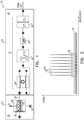
- Fig. 1 is a block diagram that schematically illustrates a multi-wavelength laser device 20, in accordance with an embodiment of the invention.
- Device 20 comprises an active optical chip 22 on a III-V semiconductor substrate 26, such as GaAs or InP, and a PIC 24 on an optical substrate 40, for example a silicon-on-insulator (SOI) substrate.
- a III-V semiconductor substrate 26 such as GaAs or InP
- a PIC 24 on an optical substrate 40, for example a silicon-on-insulator (SOI) substrate.
- SOI silicon-on-insulator
- chip 22 may be bonded to optical substrate 40, for example using a suitable adhesive.
- chip 22 and PIC 24 may be mounted separately and connected, for example, by a suitable optical fiber.
- Chip 22 comprises an RSOA 28, comprising an optical gain medium 30, which amplifies laser radiation within a certain gain band, and a reflector 36 formed at the inner end of gain medium 30.
- Application of a drive voltage between electrodes 32 and 34 gives rise to optical gain in medium 30 across a certain gain band, for example over a band of several tens of nanometers centered at around 1310 nm or 1550 nm depending on the type of gain medium that is used.
- Gain medium 30 may comprise, for example, GaInAsP, AlGaInAs quantum wells, or InAs quantum dots, which emit light in these gain bands.
- Reflector 36 may comprise a distributed Bragg reflector (DBR), for example, or a reflective coating on the rear facet of the RSOA.
- DBR distributed Bragg reflector
- a waveguide 38 on substrate 26 conveys laser radiation into and out of the RSOA at the end opposite reflector 36.
- PIC 24 comprises an external laser cavity 42, which is optically coupled to waveguide 38 and terminates in a reflector 50.
- Reflector 50 is partially reflecting to allow the multi-wavelength laser beam that is generated by device 20 to exit from the cavity.
- Cavity 42 contains a comb filter 44 and a bandpass filter 46 in series, along with a phase tuner 48 for adjusting the cavity phase.
- Comb filter 44 in this embodiment comprises an optical ring resonator, with a ring length chosen so that filter 44 passes a comb of wavelength sub-bands within the gain band of RSOA 28.
- multi-wavelength laser device 20 can serve as a beam source for WDM communication applications, for example, with the wavelength spacing between the sub-bands in the comb set equal to the spacing between the WDM channels.
- Bandpass filter 46 has a passband encompassing a subset of the wavelength sub-bands in the comb that is defined by comb filter 44.
- the subset of sub-bands encompassed by the bandpass filter may correspond to the set of wavelengths of the WDM channels, while the remainder of the comb falls outside the passband.
- the passband of the bandpass filter encompasses the subset of wavelength sub-bands in the sense that the bandpass filter attenuates the wavelengths within this subset only minimally, while applying stronger attenuation to wavelengths outside the subset.
- the passband of bandpass filter 46 is narrower than the gain band of gain medium 30. Because bandpass filter 46 is contained in the laser cavity, only a weak attenuation (on the order of 1-10 dB) is needed to suppress laser activity at wavelengths outside the passband.
- bandpass filter 46 comprises multiple optical ring resonators, having resonant wavelengths chosen to achieve the desired spectral response.
- bandpass filter 46 may comprise any other sort of filter that is suitable for implementation on PIC 24, such as an absorption filter or a diffractive filter.
- Fig. 2 is a plot that schematically shows an output spectrum of laser device 20, in accordance with an embodiment of the invention.
- the spectrum comprises a comb of equally-spaced wavelength sub-bands 54, which are encompassed by a passband 56 of bandpass filter 46.
- a reference spectrum 52 contains multiple closely-spaced lines, extending over the entire gain band of the laser.
- Intracavity comb filter 44 selects the (wider) spacing of sub-bands 54, while passband 56 suppresses the sub-bands that are outside the desired subset.
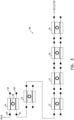
- Fig. 3 is a block diagram that schematically shows details of optical bandpass filter 46, in accordance with an embodiment of the invention.
- bandpass filter 46 comprises five optical ring resonators 70, 72, 74, 76, and 78, arranged in series. These ring resonators may be of the same type as comb filter 44, but with different spectral properties.
- the optical ring resonators are fabricated, for example, by forming silicon waveguides of suitable shapes and lengths on substrate 40 of PIC 24.
- Each optical ring resonator comprises a resonant ring 58 and four ports: a port 60 serving as an input and ports 62, 64, and 66 as outputs.
- Port 62 is referred to as a "drop port,” while port 64 is referred to as a "pass port.”
- port 64 is used as the output port, as in ring resonators 70, 72, 74, 76, and 78, destructive interference on ring 58 causes the optical ring resonator to function as a notch filter, blocking multiple sub-bands.
- each optical ring resonator depends on the length of resonant ring 58, which determines the spacing between the resonant wavelengths and hence the sub-bands that are passed or blocked. Specifically, the lengths of the resonant rings in optical ring resonators 70, 72, 74, 76, and 78 and integer quotients of the length of the resonant ring in comb filter 44, so that the spectral spacings between the resonant wavelengths of optical ring resonators 70, 72, 74, 76, and 78 are integer multiples of the comb spacing.
- n 5
- other values of n and other arrangements of optical ring resonators may be used.
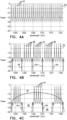
- Figs. 4A, 4B and 4C are spectral plots that schematically illustrate the operation of optical bandpass filter 46 as implemented in Fig. 3 , in accordance with an embodiment of the invention.
- the gain band of gain medium 30 in RSOA 28 is assumed to extend over a range of a few tens of nanometers in the vicinity of 1310 nm.
- Fig. 4A shows a multi-passband spectrum 80 of comb filter 44.
- Spectrum 80 comprises a comb of equally-spaced wavelength sub-bands 54, as noted above.
- Fig. 4B shows a multi-passband spectrum 82, illustrating the effect of optical ring resonator 70 on spectrum 80.
- the length of ring 58 in optical ring resonator 70 is chosen to be about 80 pm, giving rise to notches 84 that overlap and thus attenuate every fifth sub-band 54 in spectrum 80. Notches 84 effectively separate spectrum 80 into subsets of sub-bands 54 and 86.
- Fig. 4C shows the cumulative effect of optical ring resonators 72, 74, 76, and 78 on spectrum 82.
- the base wavelengths of the four optical ring resonators 72, 74, 76, and 78 are offset by one sub-band relative to one another (i.e., by about 1 nm), so that each of these optical resonators attenuates a different, respective group of sub-bands 86, spaced ten sub-bands apart.
- the base wavelengths of optical ring resonators 72, 74, 76, and 78 can be tuned to the desired offsets, for example, by heating the respective rings 58 to different temperatures, which changes their effective refractive indexes and thus shifts the resonant wavelengths.
- all of sub-bands 86 are suppressed, leaving stop-bands 88 on both sides of the selected subset of sub-bands 54.
- optical ring resonators 70, 72, 74, 76, and 78 defines a passband of bandpass filter 46 that encompasses the four desired sub-bands 54 between 1305 and 1310 nm, while suppressing unwanted sub-bands 86.
- This passband is narrower than a gain band 90 of RSOA 28 and will thus cause laser device 20 to output optical radiation in the desired sub-bands 54.
- bandpass filter 46 itself may pass additional wavelength sub-bands in peripheral parts of spectrum 80, outside stop-bands 88, the gain of the RSOA is too low in these peripheral spectral ranges to support laser activity.
- Laser device 20 thus outputs a clean spectrum consisting of radiation only in sub-bands 54, and no additional external filtering of the multi-wavelength beam is required.
- a bandpass filter may comprise one or more optical ring resonators, configured as notch filters, in conjunction with filter components of other types, such as absorptive or diffractive components.
Landscapes
- Physics & Mathematics (AREA)
- Electromagnetism (AREA)
- Optics & Photonics (AREA)
- Condensed Matter Physics & Semiconductors (AREA)
- General Physics & Mathematics (AREA)
- Engineering & Computer Science (AREA)
- Plasma & Fusion (AREA)
- Semiconductor Lasers (AREA)
Abstract
Description
- This application claims the benefit of
U.S. Provisional Patent Application 63/396,646, filed August 10, 2022 U.S. Provisional Patent Application 63/402,510, filed August 31, 2022 - The present invention relates generally to optoelectronic devices, and particularly to semiconductor lasers.
- Wavelength domain multiplexing (WDM) is commonly used in high-speed optical communications to enable multiple communication signals with different carrier wavelengths to be transmitted over the same optical fiber. Some WDM devices use a single laser, emitting radiation at a comb of wavelengths, to provide carrier waves at multiple wavelengths simultaneously. The term "comb," as used in the present description and in the claims, refers to a set of distinct spectral sub-bands, having respective center wavelengths that are spaced apart by equal steps in wavelength. The term "comb filter" refers to an optical filter having a passband consisting of such a comb, such that the comb filter passes light having a wavelength in any of the distinct spectral sub-bands in the set while blocking wavelengths between the sub-bands in the set. The terms "light" and "optical radiation" are used synonymously in the present description and in the claims to refer to electromagnetic radiation in any of the infrared, visible, and ultraviolet spectral ranges.
- For example, Zhang et al. describe a multi-wavelength laser in an article entitled "Quantum dot SOA/silicon external cavity multi-wavelength laser," published in Optics Express 23:4 (2015), pages 4666-4671. The device described in the article consists of a quantum dot reflective semiconductor optical amplifier and a silicon-on-insulator chip with a Sagnac loop mirror and microring wavelength filter. The authors showed four major lasing peaks from a single cavity.
- Some embodiments of the present invention that are described hereinbelow provide semiconductor laser devices that output optical radiation in a comb of wavelengths, as well as methods for producing and operating such devices.
- There is therefore provided, in accordance with an embodiment of the invention, an optoelectronic device, which includes a reflective semiconductor optical amplifier (RSOA), including a gain medium configured to amplify laser radiation within a given gain band, a first reflector disposed at a first end of the gain medium, and a waveguide coupled to convey the laser radiation into and out of a second end of the gain medium, opposite the first end. An external laser cavity is disposed on the optical substrate and is optically coupled to the waveguide. The external laser cavity includes a second reflector, a comb filter, disposed between the second reflector and the RSOA and configured to pass a set of distinct wavelength sub-bands within the gain band, the set of distinct wavelength sub-bands defining a comb, and a bandpass filter, disposed between the second reflector and the RSOA in series with the comb filter, the bandpass filter having a passband encompassing a subset of the wavelength sub-bands in the comb.
- In some embodiments, the RSOA includes a III-V semiconductor material, and the external laser cavity includes a silicon photonic integrated circuit (PIC). Additionally or alternatively, the external laser cavity includes a phase tuner disposed between the second reflector and the RSOA in series with the comb filter and the bandpass filter.
- In some embodiments, the comb filter includes an optical ring resonator. Additionally or alternatively, the bandpass filter includes one or more optical ring resonators, each optical ring resonator among the one or more optical ring resonators configured to filter out a selected group of the wavelength sub-bands in the comb that are outside the passband. In a disclosed embodiment, the one or more optical ring resonators include multiple optical ring resonators having different, respective resonances, which are selected so that each of the optical ring resonators filters out a different, respective subset of the wavelength sub-bands that are outside the passband.
- In the disclosed embodiments, the passband of the bandpass filter is narrower than the gain band of the gain medium.
- There is also provided, in accordance with an embodiment of the invention, a method for generating radiation. The method includes providing a reflective semiconductor optical amplifier (RSOA), including a gain medium configured to amplify laser radiation within a given gain band and a first reflector disposed at a first end of the gain medium. The RSOA is optically coupled to an external laser cavity, which is disposed on an optical substrate and includes a second reflector and a comb filter disposed between the second reflector and the RSOA and configured to pass a set of distinct wavelength sub-bands within the gain band. The set of distinct wavelength sub-bands defines a comb. A bandpass filter is disposed between the second reflector and the RSOA in series with the comb filter. The bandpass filter has a passband encompassing a subset of the wavelength sub-bands in the comb. An electrical drive is applied to the RSOA, whereby the laser radiation in subset of the wavelength sub-bands in the comb is emitted through the second reflector.
- There is additionally provided, in accordance with an embodiment of the invention, an integrated optical device, including an optical substrate and multiple optical ring resonators, which are disposed on the optical substrate and interconnected in series by waveguides. The optical ring resonators include a first optical ring resonator configured to pass a set of distinct wavelength sub-bands, the set of distinct wavelength sub-bands defining a comb, and one or more second optical ring resonators. Each second optical ring resonator among the one or more second optical ring resonators is configured to filter out a selected group of the wavelength sub-bands in the comb.
- In some embodiments, the one or more second optical ring resonators include a plurality of the second optical ring resonators having different, respective resonant wavelengths, which are selected so that each of the second optical ring resonators filters out a different, respective subset of the wavelength sub-bands in the comb by destructive interference at the respective resonant wavelengths. In a disclosed embodiment, the respective resonant wavelengths of the second optical ring resonators are selected so as to define a bandpass filter that passes a specified set of the wavelength sub-bands in the comb while attenuating the wavelengths that are outside the specified set by destructive interference in the second optical ring resonators.
- Additionally or alternatively, the first optical ring resonator includes a first resonant ring having a first length, which determines a spectral spacing of the wavelength sub-bands in the comb, and each of the second optical ring resonators includes a respective second resonant ring having a second length, which is an integer quotient of the first length.
- The present invention will be more fully understood from the following detailed description of the embodiments thereof, taken together with the drawings in which:
-
-
Fig. 1 is a block diagram that schematically illustrates a multi-wavelength laser device, in accordance with an embodiment of the invention; -
Fig. 2 is a plot that schematically shows an output spectrum of the laser device ofFig. 1 , in accordance with an embodiment of the invention; -
Fig. 3 is a block diagram that schematically shows details of an optical bandpass filter that can be used in the laser device ofFig. 1 , in accordance with an embodiment of the invention; and -
Figs. 4A, 4B and 4C are spectral plots that schematically illustrate the operation of the optical bandpass filter ofFig. 3 , in accordance with an embodiment of the invention. - Multi-wavelength semiconductor lasers that are used in WDM applications typically emit a dense comb of wavelength sub-bands over a wide spectral range. The density of the comb (i.e., the spacing between center wavelengths of the sub-bands) is determined by the laser cavity length, while the spectral range is limited mainly by the gain band of the optical gain medium in the laser. Additional filters external to the laser cavity are used to select the specific wavelength sub-bands to be used as carriers for the WDM channels and to cut off the remainder of the emission range of the laser. This approach is energy-inefficient, since much of the optical power output by the laser is discarded.
- Embodiments of the present invention that are described herein use optical filters disposed in the laser cavity to select the desired comb of sub-bands, while suppressing laser activity outside these sub-bands. These embodiments are thus able to generate a comb of sub-bands with higher spectral purity and higher efficiency than lasers relying on external filtering.
- Some of the present embodiments provide an optoelectronic device, comprising a reflective semiconductor optical amplifier (RSOA), which is coupled to an external laser cavity containing the intra-cavity filters. The RSOA typically comprises a III-V semiconductor chip, on which a gain medium is formed having a given gain band. A reflector is formed on the III-V semiconductor chip at one end of the gain medium, and a waveguide is formed at the other end to convey laser radiation into and out of the gain medium.
- The external laser cavity is formed on an optical substrate, for example on a silicon photonic integrated circuit (PIC), and is optically coupled to the waveguide on the III-V semiconductor chip. The full laser cavity is thus defined by the optical path between the reflector at one end of the gain medium of the RSOA and a second reflector on the optical substrate at the opposite end of the external laser cavity. A comb filter is formed on the optical substrate between the second reflector and the RSOA. The comb filter is designed to pass a set of distinct wavelength sub-bands, defining a comb, within the gain band of the RSOA. A bandpass filter is also formed on the optical substrate between the second reflector and the RSOA, in series with the comb filter. The bandpass filter has a passband that encompasses the desired subset of the wavelength sub-bands in the comb. As noted above, the incorporation of the comb filter and the bandpass filter in the laser cavity results in efficient concentration of laser activity in the wavelengths within the desired subset of wavelength sub-bands.
- The term "bandpass filter" is used in the present description and in the claims in its conventional sense, to mean a device that passes wavelengths within a certain range, referred to as the "passband" of the filter, and attenuates wavelengths outside the passband. The difference in attenuation applied by the bandpass filter within and outside the passband can be large or small, depending on application requirements. Generally speaking, bandpass filters having passbands with steep, sharp edges and strong attenuation outside the passband are more difficult and costly to implement than bandpass filters with passband edges that slope gradually and only moderately attenuate radiation outside the passband. An advantage of incorporating the bandpass filter internally within the laser cavity in the present embodiments is that it achieves strong suppression of wavelengths outside the passband with only moderate attenuation by the filter.
- In the embodiments that are described hereinbelow, the comb filter in the external laser cavity comprises an optical ring resonator. The resonator length is chosen to give a set of resonant wavelengths corresponding to the desired comb of wavelengths in the laser output. Such optical ring resonators can be fabricated compactly and precisely on a silicon-based optical substrate. Alternatively, other types of comb filters may be used.
- In some embodiments, the bandpass filter also comprises one or more optical ring resonators, having respective lengths chosen to filter out a selected group of the wavelength sub-bands in the comb. In a disclosed embodiment, the bandpass filter comprises multiple optical ring resonators, having different, respective lengths and thus different resonant wavelengths. The configuration and resonant wavelengths of the optical ring resonators are selected so that each of the optical ring resonators filters out a different, respective subset of the wavelength sub-bands in the comb by destructive interference (at the respective resonant wavelengths). A bandpass filter with sharp edges and strong attenuation of the wavelength sub-bands outside the desired subset can be made by appropriate selection of the resonant wavelengths of the optical ring resonators.
-
Fig. 1 is a block diagram that schematically illustrates amulti-wavelength laser device 20, in accordance with an embodiment of the invention.Device 20 comprises an activeoptical chip 22 on a III-V semiconductor substrate 26, such as GaAs or InP, and aPIC 24 on anoptical substrate 40, for example a silicon-on-insulator (SOI) substrate. For mechanical stability and compact packaging,chip 22 may be bonded tooptical substrate 40, for example using a suitable adhesive. Alternatively,chip 22 andPIC 24 may be mounted separately and connected, for example, by a suitable optical fiber. -
Chip 22 comprises anRSOA 28, comprising anoptical gain medium 30, which amplifies laser radiation within a certain gain band, and areflector 36 formed at the inner end ofgain medium 30. Application of a drive voltage betweenelectrodes medium 30 across a certain gain band, for example over a band of several tens of nanometers centered at around 1310 nm or 1550 nm depending on the type of gain medium that is used.Gain medium 30 may comprise, for example, GaInAsP, AlGaInAs quantum wells, or InAs quantum dots, which emit light in these gain bands.Reflector 36 may comprise a distributed Bragg reflector (DBR), for example, or a reflective coating on the rear facet of the RSOA. Awaveguide 38 onsubstrate 26 conveys laser radiation into and out of the RSOA at the end oppositereflector 36. -
PIC 24 comprises anexternal laser cavity 42, which is optically coupled towaveguide 38 and terminates in areflector 50.Reflector 50 is partially reflecting to allow the multi-wavelength laser beam that is generated bydevice 20 to exit from the cavity.Cavity 42 contains acomb filter 44 and abandpass filter 46 in series, along with aphase tuner 48 for adjusting the cavity phase.Comb filter 44 in this embodiment comprises an optical ring resonator, with a ring length chosen so thatfilter 44 passes a comb of wavelength sub-bands within the gain band ofRSOA 28. Thus,multi-wavelength laser device 20 can serve as a beam source for WDM communication applications, for example, with the wavelength spacing between the sub-bands in the comb set equal to the spacing between the WDM channels. -
Bandpass filter 46 has a passband encompassing a subset of the wavelength sub-bands in the comb that is defined bycomb filter 44. For example, the subset of sub-bands encompassed by the bandpass filter may correspond to the set of wavelengths of the WDM channels, while the remainder of the comb falls outside the passband. In other words, the passband of the bandpass filter encompasses the subset of wavelength sub-bands in the sense that the bandpass filter attenuates the wavelengths within this subset only minimally, while applying stronger attenuation to wavelengths outside the subset. Typically, the passband ofbandpass filter 46 is narrower than the gain band ofgain medium 30. Becausebandpass filter 46 is contained in the laser cavity, only a weak attenuation (on the order of 1-10 dB) is needed to suppress laser activity at wavelengths outside the passband. - In an embodiment that is described below, with reference to
Fig. 3 ,bandpass filter 46 comprises multiple optical ring resonators, having resonant wavelengths chosen to achieve the desired spectral response. Alternatively or additionally,bandpass filter 46 may comprise any other sort of filter that is suitable for implementation onPIC 24, such as an absorption filter or a diffractive filter. -
Fig. 2 is a plot that schematically shows an output spectrum oflaser device 20, in accordance with an embodiment of the invention. The spectrum comprises a comb of equally-spaced wavelength sub-bands 54, which are encompassed by apassband 56 ofbandpass filter 46. For comparison, areference spectrum 52 contains multiple closely-spaced lines, extending over the entire gain band of the laser.Intracavity comb filter 44 selects the (wider) spacing of sub-bands 54, whilepassband 56 suppresses the sub-bands that are outside the desired subset. -
Fig. 3 is a block diagram that schematically shows details ofoptical bandpass filter 46, in accordance with an embodiment of the invention. In the pictured example,bandpass filter 46 comprises fiveoptical ring resonators comb filter 44, but with different spectral properties. The optical ring resonators are fabricated, for example, by forming silicon waveguides of suitable shapes and lengths onsubstrate 40 ofPIC 24. - Each optical ring resonator comprises a
resonant ring 58 and four ports: aport 60 serving as an input andports outputs. Port 62 is referred to as a "drop port," whileport 64 is referred to as a "pass port." Whenport 62 is used as the output port, as incomb filter 44, constructive interference onring 58 causes the optical ring resonator to function as a bandpass filter over multiple sub-bands. Whenport 64 is used as the output port, as inring resonators ring 58 causes the optical ring resonator to function as a notch filter, blocking multiple sub-bands. - The operation of each optical ring resonator depends on the length of
resonant ring 58, which determines the spacing between the resonant wavelengths and hence the sub-bands that are passed or blocked. Specifically, the lengths of the resonant rings inoptical ring resonators comb filter 44, so that the spectral spacings between the resonant wavelengths ofoptical ring resonators optical ring resonator 70 is 1/n times the length of the resonant ring incomb filter 44, with n = 5, while the lengths of the resonant rings inoptical ring resonators comb filter 44. Alternatively, other values of n and other arrangements of optical ring resonators may be used. -
Figs. 4A, 4B and 4C are spectral plots that schematically illustrate the operation ofoptical bandpass filter 46 as implemented inFig. 3 , in accordance with an embodiment of the invention. In this example, the gain band of gain medium 30 inRSOA 28 is assumed to extend over a range of a few tens of nanometers in the vicinity of 1310 nm. -
Fig. 4A shows amulti-passband spectrum 80 ofcomb filter 44.Spectrum 80 comprises a comb of equally-spaced wavelength sub-bands 54, as noted above. The length ofring 58 incomb filter 44 is chosen to be about 400 pm, so that sub-bands are spaced apart by roughly 1 nm (assuming the ring has an effective refractive index neff = 4.3 at the 1310 nm wavelength) . -
Fig. 4B shows amulti-passband spectrum 82, illustrating the effect ofoptical ring resonator 70 onspectrum 80. The length ofring 58 inoptical ring resonator 70 is chosen to be about 80 pm, giving rise tonotches 84 that overlap and thus attenuate everyfifth sub-band 54 inspectrum 80.Notches 84 effectivelyseparate spectrum 80 into subsets ofsub-bands -
Fig. 4C shows the cumulative effect ofoptical ring resonators spectrum 82. The length Lring ofring 58 in each ofoptical ring resonators spectrum 82. The base wavelengths of the fouroptical ring resonators sub-bands 86, spaced ten sub-bands apart. The base wavelengths ofoptical ring resonators respective rings 58 to different temperatures, which changes their effective refractive indexes and thus shifts the resonant wavelengths. As a result, all of sub-bands 86 are suppressed, leaving stop-bands 88 on both sides of the selected subset ofsub-bands 54. - Thus, the combined operation of
optical ring resonators bandpass filter 46 that encompasses the four desiredsub-bands 54 between 1305 and 1310 nm, while suppressingunwanted sub-bands 86. This passband is narrower than again band 90 ofRSOA 28 and will thus causelaser device 20 to output optical radiation in the desiredsub-bands 54. Althoughbandpass filter 46 itself may pass additional wavelength sub-bands in peripheral parts ofspectrum 80, outside stop-bands 88, the gain of the RSOA is too low in these peripheral spectral ranges to support laser activity.Laser device 20 thus outputs a clean spectrum consisting of radiation only in sub-bands 54, and no additional external filtering of the multi-wavelength beam is required. - Although
Fig. 3 and4A-C show a bandpass filter with a particular configuration of optical ring resonators and a particular spectral output, the principles of this embodiment may alternatively be applied in creating selective comb filters with other configurations, for example passing different numbers and arrangements of sub-bands. Such filters offer benefits of high spectral sensitivity and low optical loss in comparison with alternative solutions that are known in the art. In further alternative embodiments, a bandpass filter may comprise one or more optical ring resonators, configured as notch filters, in conjunction with filter components of other types, such as absorptive or diffractive components. - Thus, the embodiments described above are cited by way of example, and the present invention is not limited to what has been particularly shown and described hereinabove. Rather, the scope of the present invention includes both combinations and subcombinations of the various features described hereinabove, as well as variations and modifications thereof which would occur to persons skilled in the art upon reading the foregoing description and which are not disclosed in the prior art.
The following is a list of further preferred embodiments of the invention: - Embodiment 1: An optoelectronic device, comprising:
a reflective semiconductor optical amplifier (RSOA), comprising:- a gain medium configured to amplify laser radiation within a given gain band;
- a first reflector disposed at a first end of the gain medium; and
- a waveguide coupled to convey the laser radiation into and out of a second end of the gain medium, opposite the first end;
- an optical substrate; and
- an external laser cavity, which is disposed on the optical substrate and is optically coupled to the waveguide, the external laser cavity comprising:
- a second reflector;
- a comb filter, disposed between the second reflector and the RSOA and configured to pass a set of distinct wavelength sub-bands within the gain band, the set of distinct wavelength sub-bands defining a comb; and
- a bandpass filter, disposed between the second reflector and the RSOA in series with the comb filter, the bandpass filter having a passband encompassing a subset of the wavelength sub-bands in the comb.
- Embodiment 2: The device according to embodiment 1, wherein the RSOA comprises a III-V semiconductor material, and wherein the external laser cavity comprises a silicon photonic integrated circuit (PIC).
- Embodiment 3: The device according to embodiment 1, wherein the external laser cavity comprises a phase tuner disposed between the second reflector and the RSOA in series with the comb filter and the bandpass filter.
- Embodiment 4: The device according to embodiment 1, wherein the comb filter comprises an optical ring resonator.
- Embodiment 5: The device according to embodiment 1, wherein the bandpass filter comprises one or more optical ring resonators, each optical ring resonator among the one or more optical ring resonators configured to filter out a selected group of the wavelength sub-bands in the comb that are outside the passband.
- Embodiment 6: The device according to
embodiment 5, wherein the one or more optical ring resonators comprise multiple optical ring resonators having different, respective resonances, which are selected so that each of the optical ring resonators filters out a different, respective subset of the wavelength sub-bands that are outside the passband. - Embodiment 7: The device according to embodiment 1, wherein the passband of the bandpass filter is narrower than the gain band of the gain medium.
- Embodiment 8: A method for generating radiation, the method comprising:
- providing a reflective semiconductor optical amplifier (RSOA), comprising a gain medium configured to amplify laser radiation within a given gain band and a first reflector disposed at a first end of the gain medium;
- optically coupling the RSOA to an external laser cavity, which is disposed on an optical substrate and comprises a second reflector, a comb filter disposed between the second reflector and the RSOA and configured to pass a set of distinct wavelength sub-bands within the gain band, the set of distinct wavelength sub-bands defining a comb, and a bandpass filter, disposed between the second reflector and the RSOA in series with the comb filter, the bandpass filter having a passband encompassing a subset of the wavelength sub-bands in the comb; and
- applying an electrical drive to the RSOA, whereby the laser radiation in subset of the wavelength sub-bands in the comb is emitted through the second reflector.
- Embodiment 9: The method according to embodiment 8, wherein providing the RSOA comprises forming the RSOA on a III-V semiconductor substrate, and wherein optically coupling the RSOA comprises coupling the RSOA via a waveguide to a silicon photonic integrated circuit (PIC).
- Embodiment 10: The method according to embodiment 8, and comprising coupling a phase tuner between the second reflector and the RSOA in series with the comb filter and the bandpass filter.
- Embodiment 11: The method according to embodiment 8, wherein optically coupling the RSOA comprises coupling an optical ring resonator to serve as the comb filter.
- Embodiment 12: The method according to embodiment 8, wherein optically coupling the RSOA comprises coupling one or more optical ring resonators to constitute the bandpass filter, each optical ring resonator among the one or more optical ring resonators configured to filter out a selected group of the wavelength sub-bands in the comb that are outside the passband.
- Embodiment 13: The method according to embodiment 12, wherein coupling the one or more optical ring resonators comprises coupling together multiple optical ring resonators having different, respective resonances, which are selected so that each of the optical ring resonators filters out a different, respective subset of the wavelength sub-bands that are outside the passband.
- Embodiment 14: The method according to embodiment 8, wherein optically coupling the RSOA comprises setting the passband of the bandpass filter to be narrower than the gain band of the gain medium.
- Embodiment 15: An integrated optical device, comprising:
- an optical substrate; and
- multiple optical ring resonators, which are disposed on the optical substrate and interconnected in series by waveguides, and which comprise:
- a first optical ring resonator, configured to pass a set of distinct wavelength sub-bands, the set of distinct wavelength sub-bands defining a comb; and
- one or more second optical ring resonators, each second optical ring resonator among the one or more second optical ring resonators configured to filter out a selected group of the wavelength sub-bands in the comb.
- Embodiment 16: The device according to
embodiment 15, wherein the one or more second optical ring resonators comprise a plurality of the second optical ring resonators having different, respective resonant wavelengths, which are selected so that each of the second optical ring resonators filters out a different, respective subset of the wavelength sub-bands in the comb by destructive interference at the respective resonant wavelengths. - Embodiment 17: The device according to embodiment 16, wherein the respective resonant wavelengths of the second optical ring resonators are selected so as to define a bandpass filter that passes a specified set of the wavelength sub-bands in the comb while attenuating the wavelengths that are outside the specified set by destructive interference in the second optical ring resonators.
- Embodiment 18: The device according to embodiment 16, wherein the first optical ring resonator comprises a first resonant ring having a first length, which determines a spectral spacing of the wavelength sub-bands in the comb, and wherein each of the second optical ring resonators comprises a respective second resonant ring having a second length, which is an integer quotient of the first length.
Claims (15)
- An optoelectronic device, comprising:a reflective semiconductor optical amplifier (RSOA), comprising:a gain medium configured to amplify laser radiation within a given gain band;a first reflector disposed at a first end of the gain medium; anda waveguide coupled to convey the laser radiation into and out of a second end of the gain medium, opposite the first end;an optical substrate; andan external laser cavity, which is disposed on the optical substrate and is optically coupled to the waveguide, the external laser cavity comprising:a second reflector;a comb filter, disposed between the second reflector and the RSOA and configured to pass a set of distinct wavelength sub-bands within the gain band, the set of distinct wavelength sub-bands defining a comb; anda bandpass filter, disposed between the second reflector and the RSOA in series with the comb filter, the bandpass filter having a passband encompassing a subset of the wavelength sub-bands in the comb.
- The device according to claim 1, wherein the RSOA comprises a III-V semiconductor material, and wherein the external laser cavity comprises a silicon photonic integrated circuit (PIC).
- The device according to claim 1 or 2, wherein the external laser cavity comprises a phase tuner disposed between the second reflector and the RSOA in series with the comb filter and the bandpass filter.
- The device according to any one of claims 1 to 3, wherein the comb filter comprises an optical ring resonator.
- The device according to any one of claims 1 to 4, wherein the bandpass filter comprises one or more optical ring resonators, each optical ring resonator among the one or more optical ring resonators configured to filter out a selected group of the wavelength sub-bands in the comb that are outside the passband; and/or
wherein the one or more optical ring resonators comprise multiple optical ring resonators having different, respective resonances, which are selected so that each of the optical ring resonators filters out a different, respective subset of the wavelength sub-bands that are outside the passband. - The device according to any one of claims 1 to 5, wherein the passband of the bandpass filter is narrower than the gain band of the gain medium.
- A method for generating radiation, the method comprising:providing a reflective semiconductor optical amplifier (RSOA), comprising a gain medium configured to amplify laser radiation within a given gain band and a first reflector disposed at a first end of the gain medium;optically coupling the RSOA to an external laser cavity, which is disposed on an optical substrate and comprises a second reflector, a comb filter disposed between the second reflector and the RSOA and configured to pass a set of distinct wavelength sub-bands within the gain band, the set of distinct wavelength sub-bands defining a comb, and a bandpass filter, disposed between the second reflector and the RSOA in series with the comb filter, the bandpass filter having a passband encompassing a subset of the wavelength sub-bands in the comb; andapplying an electrical drive to the RSOA, whereby the laser radiation in subset of the wavelength sub-bands in the comb is emitted through the second reflector.
- The method according to claim 7, wherein providing the RSOA comprises forming the RSOA on a III-V semiconductor substrate, and wherein optically coupling the RSOA comprises coupling the RSOA via a waveguide to a silicon photonic integrated circuit (PIC).
- The method according to claim 7 or 8, and comprising coupling a phase tuner between the second reflector and the RSOA in series with the comb filter and the bandpass filter.
- The method according to any one of claims 7 to 9, wherein optically coupling the RSOA comprises:coupling an optical ring resonator to serve as the comb filter; orcoupling one or more optical ring resonators to constitute the bandpass filter, each optical ring resonator among the one or more optical ring resonators configured to filter out a selected group of the wavelength sub-bands in the comb that are outside the passband.
- The method according to claim 10, wherein coupling the one or more optical ring resonators comprises coupling together multiple optical ring resonators having different, respective resonances, which are selected so that each of the optical ring resonators filters out a different, respective subset of the wavelength sub-bands that are outside the passband.
- The method according to any one of claims 7 to 11, wherein optically coupling the RSOA comprises setting the passband of the bandpass filter to be narrower than the gain band of the gain medium.
- An integrated optical device, comprising:an optical substrate; andmultiple optical ring resonators, which are disposed on the optical substrate and interconnected in series by waveguides, and which comprise:a first optical ring resonator, configured to pass a set of distinct wavelength sub-bands, the set of distinct wavelength sub-bands defining a comb; andone or more second optical ring resonators, each second optical ring resonator among the one or more second optical ring resonators configured to filter out a selected group of the wavelength sub-bands in the comb.
- The device according to claim 13, wherein the one or more second optical ring resonators comprise a plurality of the second optical ring resonators having different, respective resonant wavelengths, which are selected so that each of the second optical ring resonators filters out a different, respective subset of the wavelength sub-bands in the comb by destructive interference at the respective resonant wavelengths.
- The device according to claim 14, wherein the respective resonant wavelengths of the second optical ring resonators are selected so as to define a bandpass filter that passes a specified set of the wavelength sub-bands in the comb while attenuating the wavelengths that are outside the specified set by destructive interference in the second optical ring resonators; and/or
wherein the first optical ring resonator comprises a first resonant ring having a first length, which determines a spectral spacing of the wavelength sub-bands in the comb, and wherein each of the second optical ring resonators comprises a respective second resonant ring having a second length, which is an integer quotient of the first length.
Applications Claiming Priority (2)
| Application Number | Priority Date | Filing Date | Title |
|---|---|---|---|
| US202263396646P | 2022-08-10 | 2022-08-10 | |
| US202263402510P | 2022-08-31 | 2022-08-31 |
Publications (1)
| Publication Number | Publication Date |
|---|---|
| EP4322346A1 true EP4322346A1 (en) | 2024-02-14 |
Family
ID=87567588
Family Applications (1)
| Application Number | Title | Priority Date | Filing Date |
|---|---|---|---|
| EP23190826.0A Pending EP4322346A1 (en) | 2022-08-10 | 2023-08-10 | Comb laser |
Country Status (2)
| Country | Link |
|---|---|
| US (1) | US20240235155A1 (en) |
| EP (1) | EP4322346A1 (en) |
Citations (4)
| Publication number | Priority date | Publication date | Assignee | Title |
|---|---|---|---|---|
| EP3379663A2 (en) * | 2017-03-21 | 2018-09-26 | Alcatel-Lucent USA Inc. | Hybrid mode-locked laser with tunable number of comb lines |
| US20180302167A1 (en) * | 2017-04-13 | 2018-10-18 | Alcatel-Lucent Usa Inc. | Increasing fabry-perot cavity free spectral range in hybrid lasers |
| US20190181612A1 (en) * | 2013-11-20 | 2019-06-13 | Elenion Technologies, Llc | Semiconductor laser |
| US20210057880A1 (en) * | 2020-10-19 | 2021-02-25 | Intel Corporation | Multi-wavelength laser generator using ring filter |
-
2023
- 2023-08-08 US US18/366,705 patent/US20240235155A1/en active Pending
- 2023-08-10 EP EP23190826.0A patent/EP4322346A1/en active Pending
Patent Citations (4)
| Publication number | Priority date | Publication date | Assignee | Title |
|---|---|---|---|---|
| US20190181612A1 (en) * | 2013-11-20 | 2019-06-13 | Elenion Technologies, Llc | Semiconductor laser |
| EP3379663A2 (en) * | 2017-03-21 | 2018-09-26 | Alcatel-Lucent USA Inc. | Hybrid mode-locked laser with tunable number of comb lines |
| US20180302167A1 (en) * | 2017-04-13 | 2018-10-18 | Alcatel-Lucent Usa Inc. | Increasing fabry-perot cavity free spectral range in hybrid lasers |
| US20210057880A1 (en) * | 2020-10-19 | 2021-02-25 | Intel Corporation | Multi-wavelength laser generator using ring filter |
Non-Patent Citations (1)
| Title |
|---|
| ZHANG ET AL.: "describe a multi-wavelength laser in an article entitled ''Quantum dot SOA/silicon external cavity multi-wavelength laser,'' published in", OPTICS EXPRESS, vol. 23, no. 4, 2015, pages 4666 - 4671 |
Also Published As
| Publication number | Publication date |
|---|---|
| US20240235155A1 (en) | 2024-07-11 |
Similar Documents
| Publication | Publication Date | Title |
|---|---|---|
| US7835417B2 (en) | Narrow spectrum light source | |
| US6603781B1 (en) | Multi-wavelength transmitter | |
| EP3379663B1 (en) | Hybrid mode-locked laser with tunable number of comb lines | |
| US6483635B1 (en) | Apparatus for light amplification | |
| US20020071457A1 (en) | Pulsed non-linear resonant cavity | |
| JP7805732B2 (en) | Multi-wavelength laser generator using a ring filter | |
| US7149381B2 (en) | Optical filtering device and method | |
| US20030219045A1 (en) | Tunable laser using microring resonator | |
| US20070133647A1 (en) | Wavelength modulated laser | |
| WO2003043247A2 (en) | Tunable optical add/drop multiplexer with multi-function optical amplifiers | |
| WO2008080171A1 (en) | Optical transmitter having a widely tunable directly modulated laser and periodic optical spectrum reshaping element | |
| EP4042529B1 (en) | Wavelength control of multi-wavelength laser | |
| JP7709634B2 (en) | Side mode suppression for extended C-band tunable lasers - Patents.com | |
| US20030108081A1 (en) | Wavelength tunable laser light source | |
| EP1730559A1 (en) | Method and apparatus providing an output coupler for an optical beam | |
| US20240235155A1 (en) | Comb Laser | |
| JP4485745B2 (en) | Optical functional device and optical functional device | |
| US20030081639A1 (en) | Optical cavity resonating over a continuous range of frequencies | |
| CN117595078A (en) | Comb laser | |
| US20240258761A1 (en) | Laser with intracavity modulator | |
| US20050226283A1 (en) | Single-mode semiconductor laser with integrated optical waveguide filter | |
| EP4525226A1 (en) | Laser with tunable reflector | |
| US20250096530A1 (en) | Laser with Tunable Reflector | |
| EP4576456A1 (en) | Tunable reflector for a silicon photonic laser | |
| JP2017022247A (en) | Wavelength selection device and tunable light source |
Legal Events
| Date | Code | Title | Description |
|---|---|---|---|
| PUAI | Public reference made under article 153(3) epc to a published international application that has entered the european phase |
Free format text: ORIGINAL CODE: 0009012 |
|
| STAA | Information on the status of an ep patent application or granted ep patent |
Free format text: STATUS: THE APPLICATION HAS BEEN PUBLISHED |
|
| AK | Designated contracting states |
Kind code of ref document: A1 Designated state(s): AL AT BE BG CH CY CZ DE DK EE ES FI FR GB GR HR HU IE IS IT LI LT LU LV MC ME MK MT NL NO PL PT RO RS SE SI SK SM TR |
|
| STAA | Information on the status of an ep patent application or granted ep patent |
Free format text: STATUS: REQUEST FOR EXAMINATION WAS MADE |
|
| 17P | Request for examination filed |
Effective date: 20240628 |
|
| RBV | Designated contracting states (corrected) |
Designated state(s): AL AT BE BG CH CY CZ DE DK EE ES FI FR GB GR HR HU IE IS IT LI LT LU LV MC ME MK MT NL NO PL PT RO RS SE SI SK SM TR |