EP4321793A1 - Illumination device, lens, set of diffusion element and lens, and mobile body - Google Patents
Illumination device, lens, set of diffusion element and lens, and mobile body Download PDFInfo
- Publication number
- EP4321793A1 EP4321793A1 EP22784558.3A EP22784558A EP4321793A1 EP 4321793 A1 EP4321793 A1 EP 4321793A1 EP 22784558 A EP22784558 A EP 22784558A EP 4321793 A1 EP4321793 A1 EP 4321793A1
- Authority
- EP
- European Patent Office
- Prior art keywords
- light
- illumination device
- lens
- angle
- diffusion element
- Prior art date
- Legal status (The legal status is an assumption and is not a legal conclusion. Google has not performed a legal analysis and makes no representation as to the accuracy of the status listed.)
- Pending
Links
- 238000005286 illumination Methods 0.000 title claims abstract description 129
- 238000009792 diffusion process Methods 0.000 title claims abstract description 125
- 238000009826 distribution Methods 0.000 claims abstract description 66
- 230000005499 meniscus Effects 0.000 claims description 90
- 230000005855 radiation Effects 0.000 claims description 77
- 230000003287 optical effect Effects 0.000 claims description 41
- 239000007787 solid Substances 0.000 claims description 12
- 238000010586 diagram Methods 0.000 description 37
- 230000006870 function Effects 0.000 description 36
- 230000008859 change Effects 0.000 description 25
- 238000004088 simulation Methods 0.000 description 20
- 230000007423 decrease Effects 0.000 description 14
- 238000000034 method Methods 0.000 description 14
- 239000011347 resin Substances 0.000 description 13
- 229920005989 resin Polymers 0.000 description 13
- VYPSYNLAJGMNEJ-UHFFFAOYSA-N Silicium dioxide Chemical compound O=[Si]=O VYPSYNLAJGMNEJ-UHFFFAOYSA-N 0.000 description 12
- 238000004364 calculation method Methods 0.000 description 12
- 239000010419 fine particle Substances 0.000 description 11
- 238000002834 transmittance Methods 0.000 description 8
- 238000000576 coating method Methods 0.000 description 7
- 229910052681 coesite Inorganic materials 0.000 description 6
- 229910052906 cristobalite Inorganic materials 0.000 description 6
- 239000011521 glass Substances 0.000 description 6
- 229910001635 magnesium fluoride Inorganic materials 0.000 description 6
- 239000000463 material Substances 0.000 description 6
- 239000002245 particle Substances 0.000 description 6
- 239000000377 silicon dioxide Substances 0.000 description 6
- 229910052682 stishovite Inorganic materials 0.000 description 6
- 229910052905 tridymite Inorganic materials 0.000 description 6
- NAWXUBYGYWOOIX-SFHVURJKSA-N (2s)-2-[[4-[2-(2,4-diaminoquinazolin-6-yl)ethyl]benzoyl]amino]-4-methylidenepentanedioic acid Chemical compound C1=CC2=NC(N)=NC(N)=C2C=C1CCC1=CC=C(C(=O)N[C@@H](CC(=C)C(O)=O)C(O)=O)C=C1 NAWXUBYGYWOOIX-SFHVURJKSA-N 0.000 description 5
- 239000011248 coating agent Substances 0.000 description 5
- 230000002093 peripheral effect Effects 0.000 description 5
- GWEVSGVZZGPLCZ-UHFFFAOYSA-N Titan oxide Chemical compound O=[Ti]=O GWEVSGVZZGPLCZ-UHFFFAOYSA-N 0.000 description 4
- 239000012705 liquid precursor Substances 0.000 description 4
- 238000005259 measurement Methods 0.000 description 4
- 238000012806 monitoring device Methods 0.000 description 4
- 230000007480 spreading Effects 0.000 description 4
- 238000003892 spreading Methods 0.000 description 4
- 238000013461 design Methods 0.000 description 3
- 239000010410 layer Substances 0.000 description 3
- 238000004519 manufacturing process Methods 0.000 description 3
- 238000012544 monitoring process Methods 0.000 description 3
- KRHYYFGTRYWZRS-UHFFFAOYSA-N Fluorane Chemical compound F KRHYYFGTRYWZRS-UHFFFAOYSA-N 0.000 description 2
- 240000003380 Passiflora rubra Species 0.000 description 2
- 240000004050 Pentaglottis sempervirens Species 0.000 description 2
- 235000004522 Pentaglottis sempervirens Nutrition 0.000 description 2
- 230000009471 action Effects 0.000 description 2
- 210000000007 bat wing Anatomy 0.000 description 2
- 230000008901 benefit Effects 0.000 description 2
- 239000011230 binding agent Substances 0.000 description 2
- 238000001035 drying Methods 0.000 description 2
- 230000000694 effects Effects 0.000 description 2
- 238000005516 engineering process Methods 0.000 description 2
- 230000004907 flux Effects 0.000 description 2
- 230000014509 gene expression Effects 0.000 description 2
- 229910010272 inorganic material Inorganic materials 0.000 description 2
- 239000011147 inorganic material Substances 0.000 description 2
- 238000007733 ion plating Methods 0.000 description 2
- 238000003754 machining Methods 0.000 description 2
- 239000000203 mixture Substances 0.000 description 2
- 238000012986 modification Methods 0.000 description 2
- 230000004048 modification Effects 0.000 description 2
- 238000000053 physical method Methods 0.000 description 2
- 229920003229 poly(methyl methacrylate) Polymers 0.000 description 2
- 239000004926 polymethyl methacrylate Substances 0.000 description 2
- 230000008569 process Effects 0.000 description 2
- 230000009467 reduction Effects 0.000 description 2
- 238000005488 sandblasting Methods 0.000 description 2
- 239000004065 semiconductor Substances 0.000 description 2
- 239000002356 single layer Substances 0.000 description 2
- 238000004544 sputter deposition Methods 0.000 description 2
- 239000000758 substrate Substances 0.000 description 2
- PBCFLUZVCVVTBY-UHFFFAOYSA-N tantalum pentoxide Inorganic materials O=[Ta](=O)O[Ta](=O)=O PBCFLUZVCVVTBY-UHFFFAOYSA-N 0.000 description 2
- 238000007740 vapor deposition Methods 0.000 description 2
- NIYNIOYNNFXGFN-UHFFFAOYSA-N [4-(hydroxymethyl)cyclohexyl]methanol;7-oxabicyclo[4.1.0]heptane-4-carboxylic acid Chemical compound OCC1CCC(CO)CC1.C1C(C(=O)O)CCC2OC21.C1C(C(=O)O)CCC2OC21 NIYNIOYNNFXGFN-UHFFFAOYSA-N 0.000 description 1
- 239000002253 acid Substances 0.000 description 1
- 230000004075 alteration Effects 0.000 description 1
- 238000006243 chemical reaction Methods 0.000 description 1
- 238000004140 cleaning Methods 0.000 description 1
- 230000001427 coherent effect Effects 0.000 description 1
- 238000012937 correction Methods 0.000 description 1
- 238000005520 cutting process Methods 0.000 description 1
- 230000003247 decreasing effect Effects 0.000 description 1
- 238000000227 grinding Methods 0.000 description 1
- 238000010438 heat treatment Methods 0.000 description 1
- 230000007246 mechanism Effects 0.000 description 1
- 239000011022 opal Substances 0.000 description 1
- 238000005498 polishing Methods 0.000 description 1
- 239000004417 polycarbonate Substances 0.000 description 1
- 229920000515 polycarbonate Polymers 0.000 description 1
- 238000012545 processing Methods 0.000 description 1
- 230000004043 responsiveness Effects 0.000 description 1
- 230000035945 sensitivity Effects 0.000 description 1
Images









Classifications
-
- F—MECHANICAL ENGINEERING; LIGHTING; HEATING; WEAPONS; BLASTING
- F21—LIGHTING
- F21V—FUNCTIONAL FEATURES OR DETAILS OF LIGHTING DEVICES OR SYSTEMS THEREOF; STRUCTURAL COMBINATIONS OF LIGHTING DEVICES WITH OTHER ARTICLES, NOT OTHERWISE PROVIDED FOR
- F21V5/00—Refractors for light sources
- F21V5/04—Refractors for light sources of lens shape
-
- G—PHYSICS
- G02—OPTICS
- G02B—OPTICAL ELEMENTS, SYSTEMS OR APPARATUS
- G02B1/00—Optical elements characterised by the material of which they are made; Optical coatings for optical elements
- G02B1/04—Optical elements characterised by the material of which they are made; Optical coatings for optical elements made of organic materials, e.g. plastics
- G02B1/041—Lenses
-
- F—MECHANICAL ENGINEERING; LIGHTING; HEATING; WEAPONS; BLASTING
- F21—LIGHTING
- F21V—FUNCTIONAL FEATURES OR DETAILS OF LIGHTING DEVICES OR SYSTEMS THEREOF; STRUCTURAL COMBINATIONS OF LIGHTING DEVICES WITH OTHER ARTICLES, NOT OTHERWISE PROVIDED FOR
- F21V5/00—Refractors for light sources
- F21V5/008—Combination of two or more successive refractors along an optical axis
-
- G—PHYSICS
- G02—OPTICS
- G02B—OPTICAL ELEMENTS, SYSTEMS OR APPARATUS
- G02B13/00—Optical objectives specially designed for the purposes specified below
- G02B13/16—Optical objectives specially designed for the purposes specified below for use in conjunction with image converters or intensifiers, or for use with projectors, e.g. objectives for projection TV
-
- G—PHYSICS
- G02—OPTICS
- G02B—OPTICAL ELEMENTS, SYSTEMS OR APPARATUS
- G02B27/00—Optical systems or apparatus not provided for by any of the groups G02B1/00 - G02B26/00, G02B30/00
- G02B27/09—Beam shaping, e.g. changing the cross-sectional area, not otherwise provided for
- G02B27/0916—Adapting the beam shape of a semiconductor light source such as a laser diode or an LED, e.g. for efficiently coupling into optical fibers
-
- G—PHYSICS
- G02—OPTICS
- G02B—OPTICAL ELEMENTS, SYSTEMS OR APPARATUS
- G02B3/00—Simple or compound lenses
- G02B3/0006—Arrays
- G02B3/0037—Arrays characterized by the distribution or form of lenses
- G02B3/0056—Arrays characterized by the distribution or form of lenses arranged along two different directions in a plane, e.g. honeycomb arrangement of lenses
-
- G—PHYSICS
- G02—OPTICS
- G02B—OPTICAL ELEMENTS, SYSTEMS OR APPARATUS
- G02B5/00—Optical elements other than lenses
- G02B5/02—Diffusing elements; Afocal elements
- G02B5/0205—Diffusing elements; Afocal elements characterised by the diffusing properties
- G02B5/021—Diffusing elements; Afocal elements characterised by the diffusing properties the diffusion taking place at the element's surface, e.g. by means of surface roughening or microprismatic structures
-
- G—PHYSICS
- G02—OPTICS
- G02B—OPTICAL ELEMENTS, SYSTEMS OR APPARATUS
- G02B5/00—Optical elements other than lenses
- G02B5/02—Diffusing elements; Afocal elements
- G02B5/0205—Diffusing elements; Afocal elements characterised by the diffusing properties
- G02B5/021—Diffusing elements; Afocal elements characterised by the diffusing properties the diffusion taking place at the element's surface, e.g. by means of surface roughening or microprismatic structures
- G02B5/0215—Diffusing elements; Afocal elements characterised by the diffusing properties the diffusion taking place at the element's surface, e.g. by means of surface roughening or microprismatic structures the surface having a regular structure
-
- G—PHYSICS
- G02—OPTICS
- G02B—OPTICAL ELEMENTS, SYSTEMS OR APPARATUS
- G02B9/00—Optical objectives characterised both by the number of the components and their arrangements according to their sign, i.e. + or -
- G02B9/12—Optical objectives characterised both by the number of the components and their arrangements according to their sign, i.e. + or - having three components only
- G02B9/14—Optical objectives characterised both by the number of the components and their arrangements according to their sign, i.e. + or - having three components only arranged + - +
- G02B9/30—Optical objectives characterised both by the number of the components and their arrangements according to their sign, i.e. + or - having three components only arranged + - + the middle component being a - compound meniscus having a + lens
-
- F—MECHANICAL ENGINEERING; LIGHTING; HEATING; WEAPONS; BLASTING
- F21—LIGHTING
- F21V—FUNCTIONAL FEATURES OR DETAILS OF LIGHTING DEVICES OR SYSTEMS THEREOF; STRUCTURAL COMBINATIONS OF LIGHTING DEVICES WITH OTHER ARTICLES, NOT OTHERWISE PROVIDED FOR
- F21V5/00—Refractors for light sources
- F21V5/002—Refractors for light sources using microoptical elements for redirecting or diffusing light
- F21V5/004—Refractors for light sources using microoptical elements for redirecting or diffusing light using microlenses
-
- F—MECHANICAL ENGINEERING; LIGHTING; HEATING; WEAPONS; BLASTING
- F21—LIGHTING
- F21Y—INDEXING SCHEME ASSOCIATED WITH SUBCLASSES F21K, F21L, F21S and F21V, RELATING TO THE FORM OR THE KIND OF THE LIGHT SOURCES OR OF THE COLOUR OF THE LIGHT EMITTED
- F21Y2115/00—Light-generating elements of semiconductor light sources
- F21Y2115/30—Semiconductor lasers
Definitions
- the present invention relates to an illumination device.
- an illumination device using a laser as a light source is used as illumination of an in-vehicle peripheral monitoring sensor, an in-vehicle monitoring sensor, or a monitoring sensor that monitors a moving body such as a person in a facility such as a hospital or a factory.
- Such an illumination device is required to increase the spread of a beam of laser light and to emit light at a wide angle (for example, 180°) in order to illuminate as wide a range as possible with the laser light emitted from one light source.
- the wide angle includes, for example, a wide angle in a horizontal direction and a wide angle in a vertical direction in addition to the horizontal direction.
- a diffusion plate such as a frost type or an opal type for diffusing light
- a diffusion element such as a microlens array, a microprism array, or a DOE
- Patent Document 1 discloses a laser illumination device including a laser light source, a microelement lens that spreads laser light from the laser light source, and a meniscus lens having negative power that spreads laser light from the microelement lens, for the purpose of securing safety of human eyes.
- Patent Document 1 Japanese Patent Application Publication No. 2018-133138
- the meniscus lens having negative power is installed behind the microelement lens for the purpose of increasing an apparent light source size projected onto the human eyes and securing safety to the eyes.
- a light distribution angle is only described as a wide angle (for example, 140°), and a configuration for further spreading light is not disclosed.
- the present invention has been made in view of such a situation, and an object thereof is to provide an illumination device capable of spreading light at a wider angle.
- an illumination device includes: a light source that emits parallel light or divergent light; a diffusion element that receives the light emitted from the light source and emits the light at a diffusion angle of 50° or more and 110° or less; and a lens group that has negative power, receives the light from the diffusion element by a first surface, and emits the light from a second surface at a light distribution angle of 140° or more.
- an illumination device capable of spreading light at a wider angle.
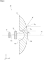
- Fig. 1 is a schematic cross-sectional view of an illumination device 10 according to an embodiment of the present invention.
- Fig. 2 is a schematic perspective view of the illumination device 10 according to the embodiment of the present invention.
- the illumination device 10 includes a light source 12, a diffusion element 14, and a lens group 16.
- the light source 12 emits parallel light or divergent light.
- the light source 12 can be a laser light source that emits particularly coherent laser light.
- the diffusion element 14 receives the light emitted from the light source 12 and emits the light at a diffusion angle of 50° or more and 110° or less.
- the diffusion element 14 may have a plate shape, and may be a microlens array including a plurality of microlenses on any principal surface of a plate in particular.
- the lens group 16 has negative power.
- the lens group 16 receives the light emitted from the diffusion element 14 and emits the light at a light distribution angle of 140° or more.
- the lens group 16 can be a single meniscus lens in particular.
- the "lens group” may include one or a plurality of lenses, and in a case where the lens group includes a plurality of lenses, the lens group represents a group of the plurality of lenses.
- the total light transmittance of the diffusion element 14 including the microlens decreases when the diffusion angle increases.
- the total light transmittance of the lens group 16 when the diffusion angle increases, an incidence angle on a lens surface increases and the reflectance increases, so that the transmittance decreases.
- the light source 12 is a laser light source, and an axis on which an intensity distribution of the light emitted from the light source 12 is symmetric is an optical axis Ax of the illumination device 10.
- the optical axis Ax may be perpendicular to a light emission surface 12a of the light source 12 and may pass through the center of the light emission surface 12a.
- coordinate axes of X, Y, and Z are defined such that a direction parallel to the optical axis Ax is a Z direction, a direction perpendicular to the Z direction and parallel to a paper surface is a Y direction, and a direction perpendicular to the paper surface is an X direction.
- the lens group 16 is a single lens or a single lens equivalent to the lens group 16, a surface that receives light emitted from the diffusion element 14 is a first surface 16a, and a surface that substantially faces the first surface 16a and emits light is a second surface 16b.
- the lens group 16 is a single lens of a meniscus lens
- the curvature is the reciprocal of a paraxial radius when a paraxial region of each surface is approximated to a spherical surface.
- the meniscus lens when
- Fig. 3 is a diagram for defining angles of light emitted from the components of the illumination device 10 with respect to the optical axis.
- angles of the light emitted from the diffusion element 14 and the first surface 16a and the second surface 16b of the lens group 16 with respect to a Z axis are ⁇ 1 , ⁇ 2 , and ⁇ 3 , respectively.
- ⁇ 1 is less than 25° (less than 50° in the diffusion angle)
- the second surface 16b of the lens group 16 becomes a flat surface or a concave surface, and the reflectance at the interface becomes very large.
- light use efficiency of the entire illumination device 10 decreases.
- ⁇ 1 is preferably 25° or more and 55° or less (50° ⁇ 2 ⁇ ⁇ 1 ⁇ 110°).
- a light distribution angle that is a maximum value of 2 ⁇ ⁇ 3 may be 160° or more and 180° or less.
- the illumination device 10 satisfies the following Formula (1) for ⁇ 1 to ⁇ 3 . ⁇ 2 ⁇ ⁇ 1 ⁇ ⁇ 3 ⁇ ⁇ 2
- a left side of Formula (1) represents a change amount in the angle of light on the first surface 16a of the lens group 16, and a right side of Formula (1) represents a change amount in the angle of light on the second surface 16b of the lens group 16.
- ⁇ 1 large
- the inclination angle of the first surface 16a exceeds 90°, and it becomes difficult to manufacture the lens group 16.
- the optimum condition is that the inclination angle of the first surface 16a is 90° or less and ⁇ 2 - ⁇ 1 is as close as possible to ⁇ 3 - ⁇ 2 .
- the illumination device 10 satisfies the following Formula (2) for F 3 ( ⁇ 3 ).
- R 21 ( ⁇ 1 ) is a reflection loss at the first surface 16a of the lens group 16
- R 32 ( ⁇ 2 ) is a reflection loss at the second surface 16b of the lens group
- F 1 ( ⁇ 1 ) is an intensity of light emitted from the diffusion element 14 per unit solid angle
- F 2 ( ⁇ 2 ) is an intensity of light emitted from the second surface 16b of the lens group 16 per unit solid angle.
- ⁇ 1 , ⁇ 2 , and ⁇ 3 are minute angles of ⁇ 1 , ⁇ 2 , and ⁇ 3 , respectively.
- Fig. 4 is a diagram illustrating a relation between an angle ⁇ of a light beam L with respect to the Z axis and an azimuth angle ⁇ of the light beam L.
- Formula (2) is based on the premise that F 1 ( ⁇ 1 ), F 2 ( ⁇ 2 ), and F 3 ( ⁇ 3 ) are constant regardless of the azimuth angle ⁇ .
- F 3 ( ⁇ 3 ) when the intensity of light emitted from the illumination device 10 per unit solid angle is F 3 ( ⁇ 3 ), F 3 ( ⁇ 3 ) may increase with an increase in ⁇ 3 while Formula (2) is satisfied.
- ⁇ 3 it may be desirable to change the light intensity according to ⁇ 3 .
- a distance to a person immediately below the monitoring device is short, and a distance to a person obliquely below the monitoring device is long.
- a range that can be monitored can be expanded by increasing the intensity of light directed obliquely below rather than immediately below the illumination device attached downward.
- a function that increases with the increase in ⁇ 3 is not limited thereto, and examples thereof include a function represented by the following Formula (3A).
- F 3 ⁇ 3 cos ⁇ 3 ⁇ 2
- n a positive real number
- a light source having high directivity such as a surface emitting laser (VCSEL) or an edge emitting laser diode can be used.
- a combination of a light emitting element having low directivity such as an LED and a collimating lens can be used as the light source 12.
- the VCSEL or the laser may include an array in which a plurality of light emitting points or light emitting elements are arranged in one case.
- the light emitted from the light source 12 does not need to be completely collimated, and may be divergent light spreading to, for example, about 20°.
- the light source 12 has a light emission surface (light emitting surface) 12a, and emits light from the light emission surface 12a with a luminous intensity distribution in a predetermined angle.
- An axis along which the luminous intensity distribution is substantially symmetrical is defined as the optical axis Ax.
- the optical axis Ax may be perpendicular to the light emission surface 12a, may be perpendicular to a bottom surface of a part of a case of the light source 12, and may pass through the center of the light emission surface 12a.
- the light source 12 is usually disposed such that the optical axis Ax is parallel to the Z axis of orthogonal coordinate axes, and the illumination device 10 and the components included therein are described.
- a light emitting element including a semiconductor such as a laser or an LED is used as the light source 12
- the light emitting element is small in size and power consumption is small.
- a light source such as an incandescent lamp or a fluorescent lamp that emits light by, for example, resistance heating.
- the structure of the diffusion element 14 is not limited as long as the diffusion element 14 receives the light emitted from the light source 12 and emits light with an expanded spread angle.
- a frosted diffusion plate having a shape of a flat plate made of glass, resin, or the like and having a roughened surface by grinding, polishing, or sandblasting, a corrosion-type diffusion plate having a surface corroded with hydrofluoric acid or the like and having a predetermined roughness
- an opal-type diffusion plate having a surface of a flat plate made of glass or resin and having a milky white, white, or gray film formed on the surface, or the like can be used.
- a substrate made of glass, resin, or the like and having a surface provided with an irregularity structure such as a large number of minute microlenses or microprisms can also be used as the diffusion element 14 from the viewpoint of good performance and control.
- the diffusion element 14 including a microlens array has a surface on which minute lenses (microlenses) are randomly disposed or a surface on which cylindrical lenses are arranged.
- each microlens may be convex or concave, or a mixture of a convex lens and a concave lens.
- the size of the microlens in the diffusion element 14 does not need to be uniform, and the height of the lens may also be different. As long as a predetermined diffusion angle is obtained and uniform light intensity is obtained in a necessary direction, an outer shape (plan view) when the microlens is viewed from the incidence side may be a polygon, a circle, an ellipse, or a mixture thereof. Further, a gap may be provided between the microlenses.
- a diameter of each microlens in the diffusion element 14 may be several um to several hundred um, and may be, for example, 10 um to 200 ⁇ m.
- the microlens array in the diffusion element 14 may be a microlens array in which microlenses are formed using a mold using resin or glass as a material, a microlens array in which resin is poured into a mold and molded, a microlens array in which a surface of glass is etched with acid, a microlens array formed by forming minute irregularities by sandblasting, or the like.
- the microlens may be formed of a material that is transparent at a light wavelength of the light source 12, and does not need to be transparent at the other wavelengths.
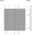
- Figs. 5(a) and 5(b) are diagrams for explaining the diffusion element 14.
- Fig. 5(a) is a schematic front view of the diffusion element 14
- Fig. 5(b) is a schematic cross-sectional view taken along the line A-A of the diffusion element 14 illustrated in Fig. 5(a) .
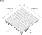
- Fig. 6 is a bird's-eye view illustrating a part of the diffusion element 14.
- the diffusion element 14 is a microlens array including a plate 20 and a large number of microlenses 22 formed on a surface of the plate 20.
- the diffusion element 14 illustrated here has a quadrangular shape in front view, but the shape thereof is not limited as long as the diffusion element has a size sufficient to receive light from the light source 12, and may be a circle, an ellipse, or the like in addition to a polygon.
- the microlenses 22 may be formed on the front and rear principal surfaces of the plate 20, and in this case, diffusion efficiency can be improved.
- the microlens 22 may be formed on a surface of a refractive-type convex lens or concave lens, and in this case, the diffused light can be refracted, and the enlargement and reduction of the diffusion angle can be controlled.
- the diffusion element 14 may include these microlenses 22.
- the diffusion element 14 may include fine particles (diffusive particles) having a size capable of scattering light inside the diffusion element 14 in addition to the microlenses 22, so that diffusing power of the diffusion element 14 can be improved. Even when a film containing diffusion particles is formed on the surface of the diffusion element 14 or the surface of the microlens 22, similar effects can be expected.
- the size of the fine particles capable of scattering light may be about 1 nm to 100 nm in a case of Rayleigh scattering, and may be equal to or more than 1 nm to 100 nm, or about 1 um to 100 um in a case of Mie scattering.
- the fine particles include resin such as PMMA, fine particles made of SiO 2 or MgF 2 , and hollow particles thereof.
- an antireflection film (including a thing that suppresses reflection even if the reflectance does not become substantially 0) for suppressing reflection and improving light transmittance may be formed on the surface of the diffusion element 14.
- the antireflection film is obtained by coating the surface of the diffusion element with an inorganic material such as MgF 2 , SiO 2 , TiO 2 , or Ta 2 O 5 or a material such as a resin in a single layer or multiple layers.
- the antireflection film can also be obtained by coating a layer containing fine particles containing hollow or solid SiO 2 , MgF 2 , or the like in a binder.
- a coating method in addition to physical methods such as vacuum vapor deposition, sputtering, and ion plating, a method of applying a liquid precursor of a film to a surface and drying the liquid precursor can be used.
- the lens group 16 includes a lens system that receives light emitted at a predetermined spread angle by the diffusion element 14 and expands the spread angle to emit light.
- the lens system having a function of expanding the spread angle is generally a concave lens system.
- the concave lens system is a lens system having negative power.
- the lens group 16 includes one or more lenses, and may include a lens group in which surfaces are bonded to each other. In the adjacent lenses, a layer having a refractive index different from that of the lens may be included between the surfaces.
- the lens group 16 includes one axisymmetric lens (single lens), a plano- concave lens, a biconcave lens, a concave-convex lens, and the like can be exemplified.
- a part of the concave-convex lens may be referred to as a meniscus lens, and the meniscus lens having negative power may be particularly a meniscus lens in which a thickness of a peripheral portion is larger than a thickness of a center portion.
- the meniscus lens has a part of functions action of a concave lens and a convex lens, it is generally known that spherical aberration can be caused to be smaller than that of a plano - concave lens or the like, and there is an advantage in that a spread angle thereof can be easily controlled.
- the lens group 16 may be formed of a material that is transparent at a light wavelength of the light source 12, does not need to be transparent at the other wavelengths, and may be formed using resin or glass as a material.
- the lens group 16 by including fine particles (diffusion particles) having a size capable of scattering light in the lens, it is possible to expand the spread angle by the lens group 16 by the light diffusion action. Even when a film containing diffusion particles is formed on the lens surface, similar effects can be expected.
- the size of the fine particles capable of scattering light is as described above.
- the fine particles may be colorless or transparent fine particles, and in addition to a resin such as PMMA, fine particles made of SiO 2 or MgF 2 can be used, and these hollow particles can also be used.
- an antireflection film (including a thing that suppresses reflection even if the reflectance does not become substantially 0) for suppressing reflection and improving light transmittance may be formed on the surface of the lens group 16.
- the antireflection film is obtained by coating the surface of the lens with an inorganic material such as MgF 2 , SiO 2 , TiO 2 , or Ta 2 O 5 or a material such as a resin in a single layer or multiple layers.
- the antireflection film can also be obtained by coating a layer containing fine particles containing hollow or solid SiO 2 , MgF 2 , or the like in a binder.
- a coating method in addition to physical methods such as vacuum vapor deposition, sputtering, and ion plating, a method of applying a liquid precursor of a film to a surface and drying or curing the liquid precursor to fix the film can be used.
- the illumination device 10 includes the light source 12, the diffusion element 14 that receives light emitted from the light source 12 and emits the light at a predetermined spread angle, and the lens group 16 that receives the light emitted from the diffusion element 14 and emits the light at an expanded predetermined spread angle.
- the illumination device 10 in which a laser (VCSEL array; light emitting points of a large number of VCSEL-type semiconductor lasers are arranged in an array and integrated in a case) having a light emission surface of about 1 mm ⁇ 1 mm is used as the light source 12, a microlens array having a substantially flat shape as illustrated in Fig. 5(a) is used as the diffusion element 14, and one axisymmetric meniscus lens is used as the lens group 16 will be described as an example.
- a laser VCSEL array; light emitting points of a large number of VCSEL-type semiconductor lasers are arranged in an array and integrated in a case
- a microlens array having a substantially flat shape as illustrated in Fig. 5(a) is used as the diffusion element 14
- one axisymmetric meniscus lens is used as the lens group 16 will be described as an example.
- the light source 12 is disposed in a space including the orthogonal coordinate axes such that the optical axis Ax is parallel to the Z direction (the optical axis Ax may be the Z axis).
- the diffusion element 14 is disposed such that the optical axis Ax of the light source 12 passes through the geometric center of the diffusion element 14 and light is received from the light source 12.
- a light receiving surface of the diffusion element 14 preferably has a size sufficient to receive the light emitted from the light source 12 in a necessary range or almost all the light.
- the diffusion element 14 including a microlens array has a size of 0.25 mm ⁇ 0.25 mm to 5 mm ⁇ 5 mm in plan view, has a substantially parallel flat plate shape with a thickness of 0.1 mm to 3 mm, and has a large number of microlenses formed on at least one surface.
- the size of each microlens is 2.5 um to 100 um, and the Sag amount (height of the microlens) is 5 um to 500 ⁇ m.
- the meniscus lens 16 is disposed such that the symmetry axis of the lens (which may be the optical axis of the lens) is matched with the axis Ax of the light source and a surface having a concave shape faces the diffusion element 14.
- the meniscus lens 16 has, for example, a diameter of 5 mm to 50 mm and a center thickness of 0.25 mm to 15 mm.
- the illumination device 10 may include a housing (not illustrated) that integrally holds these components and other components.
- the light incident on the diffusion element 14 from the light source 12 is diffused by the microlenses or the like arranged in the diffusion element 14 and spreads in a predetermined range. As illustrated in Figs. 1 and 2 , the light emitted from the diffusion element 14 spreads inside a cone, a pyramid, a truncated cone, or a truncated pyramid that is substantially symmetric with respect to the optical axis Ax.
- the intensity of the light emitted from the diffusion element 14 may change depending on the angle ( ⁇ 1 ) formed with the Z axis, but it is desirable that the light intensity is constant regardless of ⁇ 1 because it is easy to design the meniscus lens 16 at the subsequent stage (rear lens).
- the light intensity may be constant in a direction ( ⁇ direction) rotating about the Z axis.
- ⁇ direction rotating about the Z axis.
- an angle ( ⁇ 1 ) formed by the light emitted from the diffusion element 14 and the Z axis (optical axis Ax) is defined as a divergence angle.
- the diffusion angle of the diffusion element 14 including the microlenses is preferably 50° or more and 110° or less. If the diffusion angle is less than 50°, the reflection loss on the lens surface when light is spread by the meniscus lens 16 at the subsequent stage increases, and if the diffusion angle exceeds 110°, the reflection loss in the diffusion element 14 increases, and the total amount of light emitted from the illumination device 10 decreases.
- the light spread to a predetermined diffusion angle by the diffusion element 14 is incident on the first surface (light receiving surface) 16a of the meniscus lens 16 and is refracted to increase the divergence angle.
- the light reaches the second surface (emission surface) (16b) from the inside of the lens, is refracted, and is emitted.
- tracking of the light beam emitted from the light source 12 is considered.
- the light emitted from the light emission surface 12a of the light source 12 (for example, the light beam parallel to the optical axis Ax) is spread to an angle of the divergence angle ⁇ 1 by the diffusion element 14, spread to ⁇ 2 by the first surface 16a of the meniscus lens 16, and spread to ⁇ 3 by the second surface 16b of the meniscus lens 16.
- ⁇ 1 to ⁇ 3 are angles formed with the Z axis (optical axis).
- a maximum value ( ⁇ 1max ) of ⁇ 1 becomes 1/2 of the diffusion angle of the diffusion element 14.
- maximum values ⁇ 2max and ⁇ 3max of divergence angles of the first surface 16a and the second surface 16b of the meniscus lens 16 are also 1/2 of the diffusion angles of the first surface 16a and the second surface 16b of the meniscus lens 16, respectively.
- Fig. 7 is a conceptual diagram illustrating a light flux emitted from the diffusion element 14. Consideration is given to light included in an annulus having divergence angles of ⁇ 1 and ⁇ 1 + ⁇ 1 (where ⁇ 1 is a minute angle) emitted from the diffusion element 14. The light intensity distribution after passing through the diffusion element 14 is defined as F 1 ( ⁇ 1 ). Since the light intensity distribution is symmetric with respect to the Z axis, F 1 ( ⁇ 1 ) is constant even if the azimuth ( ⁇ ) changes.
- E( ⁇ 1 ) passing through the annulus of ⁇ 1 and ⁇ 1 + ⁇ 1 is represented by the following Formula (4) when ⁇ 1 is sufficiently small.
- Reflection loss occurs on the first surface 16a and the second surface 16b of the meniscus lens 16.
- R 21 ( ⁇ 1 ) the reflection loss occurring on the first surface 16a
- R 32 ( ⁇ 2 ) the reflection loss occurring on the second surface 16b
- the following Formulas (7) and (8) are established.
- F 3 ( ⁇ 3 ) may be a function that monotonically increases while satisfying Formula (10).
- a function shown in the following Formula (11) or Formula (12) or a function shown in the above Formula (3C) is considered.
- F 3 ⁇ 3 cos ⁇ 3 ⁇ 2
- F 3 ⁇ 3 cos ⁇ 3 ⁇ 3
- F 3 ( ⁇ 3 ) constant value is set, uniform illumination is obtained, and if F 3 ( ⁇ 3 ) is set to a function that increases as ⁇ 3 increases, the illumination device 10 in which the radiation intensity changes according to the function is obtained.
- Formula (13) determines the shape of the lens surface of the meniscus lens 16 for various F 1 ( ⁇ 1 ), F 2 ( ⁇ 2 ), and F 3 ( ⁇ 3 ).
- F 1 ( ⁇ 1 ) is constant regardless of ⁇ 1
- F 3 ( ⁇ 3 ) is also constant regardless of ⁇ 3
- Formula (14) is obtained from Formula (13).
- ⁇ ⁇ 3 ⁇ sin ⁇ 3 C ⁇ ⁇ ⁇ 1 ⁇ sin ⁇ 1
- C is a constant.
- ⁇ 3 corresponding to ⁇ 1 can be sequentially obtained from the center of the meniscus lens 16 toward the outside.
- the constant C is determined so as to be a target ⁇ 3 at a predetermined ⁇ 1 . In this way, ⁇ 3 corresponding to ⁇ 1 is obtained. Even when there is the reflection loss on the lens surface of the meniscus lens 16 or when F 3 ( ⁇ 3 ) is not constant, ⁇ 3 corresponding to ⁇ 1 can be similarly obtained by using Formulas (11) and (12).
- ⁇ 2 can take various values.
- ⁇ 2 ⁇ 1
- the light is not spread at all on the first surface 16a of the meniscus lens 16, and the light is largely bent on the second surface 16b.
- ⁇ 2 ⁇ ⁇ 1 is also established in a mathematical expression. At this time, the light spread to ⁇ 1 is once narrowed to ⁇ 2 and again spread, and the reflection loss on the lens surface increases, so that the transmittance greatly decreases.
- the shapes of the first surface 16a and the second surface 16b of the meniscus lens 16 can be obtained by tracking of the light beam when ⁇ 1 , ⁇ 2 corresponding to ⁇ 1 , and ⁇ 3 corresponding to ⁇ 2 are determined.
- ⁇ 1 , ⁇ 2 corresponding to ⁇ 1 , and ⁇ 3 corresponding to ⁇ 2 are determined.
- an incidence angle on the lens surface is uniquely determined according to the law of refraction, and an angle formed by the lens surface and the Z axis at that time is also uniquely determined.
- ⁇ 1 is increased by ⁇ 1 , the angle formed by the lens surface through which the light passes and the Z axis can be calculated, and as a result, all inclination angles of the lens surface through which the light passes at the angle of ⁇ 1 are obtained.
- the inclination angle of the lens surface at the center of the meniscus lens 16 is determined. For this reason, if the lens coordinates are determined so that the lens surfaces are smoothly connected from the coordinates toward the outer peripheral direction, that is, a differential coefficient of the lens surface continuously changes, the surface shape of the meniscus lens 16 can be determined. For the second surface 16b of the meniscus lens 16, the shape of the lens surface can be determined by similar calculation.
- the optimum ⁇ 2 can be determined by the following method.
- the light traveling direction is deflected by ⁇ 2 - ⁇ 1 .
- ⁇ 3 ⁇ 1 + ⁇ ⁇ 21 + ⁇ ⁇ 32
- Formula (15) represents that the light spread to ⁇ 1 by the diffusion element 14 is spread more by ⁇ 21 on the first surface 16a of the meniscus lens 16, and is further spread by ⁇ 32 on the second surface 16b of the meniscus lens 16.
- the amount deflected by the diffusion element 14 and the first surface 16a and the second surface 16b of the meniscus lens 16 is defined as a contribution ratio of each element by the following Formulas (16) to (18).
- ⁇ 1 ⁇ 1 / ⁇ 3
- ⁇ 21 ⁇ ⁇ 21 / ⁇ 3
- ⁇ 32 ⁇ ⁇ 32 / ⁇ 3
- the light radiation efficiency of the illumination device 10 is calculated with various combinations of ⁇ 1 , ⁇ 21 , and ⁇ 32 .
- the light radiation efficiency represents light energy radiated from the illumination device 10 through the meniscus lens 16 when light energy radiated from the light source 12 is set to 1.
- the light energy is obtained by integrating light energy radiated not only in a certain ⁇ 3 direction but also in all directions.
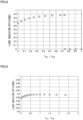
- Fig. 8 illustrates an example of a calculation result of the light radiation efficiency of the illumination device 10.
- a vertical axis of a graph represents light radiation efficiency
- a horizontal axis of the graph represents ⁇ 21 / ⁇ 32 .
- the light radiation efficiency is 0, which means that the inclination angle of the first surface of the meniscus lens is 90° or more, and it is difficult to manufacture the lens, so that it is in a range that cannot be realized.
- Fig. 9 illustrates another example of the calculation result of the light radiation efficiency of the illumination device 10.
- an angle to be deflected by the meniscus lens 16 is smaller than that in the example illustrated in Fig. 8 .
- the inclination angle of the first surface 16a of the meniscus lens 16 does not exceed 90°, so that the meniscus lens 16 can be manufactured in a wide range of ⁇ 21 / ⁇ 32 .
- the light radiation efficiency of the illumination device 10 can be similarly calculated, and when conditions under which the light radiation efficiency is maximized are obtained for each combination, ⁇ 21 ⁇ ⁇ 32 is satisfied.
- an equal sign in Formula (19) is established when the inclination angle of the first surface 16a of the meniscus lens 16 is 90° or less, and represents that the light radiation efficiency increases when ⁇ 21 is increased as much as possible in a range in which the inclination angle of the first surface 16a of the meniscus lens 16 does not exceed 90°.
- ⁇ 2 where the light radiation efficiency is highest for different ⁇ 1 and ⁇ 3 .
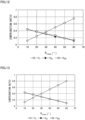
- Figs. 10 to 14 illustrate results of calculating a combination of ⁇ 1max , ⁇ 2max , and ⁇ 3max where the light radiation efficiency of the illumination device 10 is maximized.
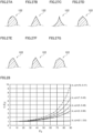
- Fig. 15 illustrates the light radiation efficiency of the illumination device 10 with contour lines under each condition of Figs. 10 to 14 .
- ⁇ 3max increases, the light radiation efficiency decreases, and at the same time, ⁇ 1max at which the light radiation efficiency is maximized increases.
- ⁇ 3max is 90°
- ⁇ 3max is 70°
- the light radiation efficiency is maximized (about 0.81) at ⁇ 1max around 30°.
- a CV value is preferably 0.05 or less, more preferably 0.04 or less, and particularly preferably 0.035 or less.
- the light source 12, the diffusion element 14, and the lens group 16 were designed, and simulation was performed as to what light distribution characteristics can be obtained as the illumination device 10.
- OpticsStudio 5 Ver20.1 manufactured by Zemax was used.
- NIR-VCSEL Part Number: V0081 manufactured by Vixar was used.
- This light source emits near-infrared light having a dominant wavelength of 940 nm.
- this light source has an array shape in which a plurality of light emitting areas are arranged in a hexagonal close-packed manner, and is an aggregate of a total of 281 VCSEL light emitters, and the size of the light emitter (light emitting surface) is about 1.0 mm ⁇ 1.0 mm.
- Fig. 16 illustrates a light intensity distribution of light emitted from the light source used in the simulation.
- the light intensity distribution is substantially axisymmetric.
- the FWHM full width at half maximum
- a substantially toroidal distribution indicating the maximum light intensity distribution at a predetermined emission angle is shown.
- a plate-shaped microlens array in which a plurality of microlenses are formed on one surface was used.
- Fig. 17 is a plan view of a range of 0.25 mm ⁇ 0.25 mm of the microlens array used in the simulation.
- Fig. 18 is a partial cross-sectional view of the microlens array illustrated in Fig. 17 .
- the microlens array has a principal surface of 1 mm ⁇ 1 mm and a plate shape with a thickness of 0.4 mm, and a plurality of convex microlenses are formed on one side of the principal surface.
- the microlens array has an average arrangement pitch of about 24 um, and is formed randomly.
- the microlens is an axisymmetric convex surface, and a basic shape thereof is represented by the following Formula (24).
- Z C ⁇ r 2 1 + 1 ⁇ 1 + K ⁇ C 2 ⁇ r 2 + a 2 ⁇ r 2 + a 4 ⁇ r 4 + a 6 ⁇ r 6
- each microlens was formed so as to randomly have a variation of ⁇ 9 um in a direction parallel to the principal surface and ⁇ 1 um in a direction perpendicular to the principal surface.
- a mold in which the unevenness of the lens shape of the microlens array is reversed was prepared, and cast on one surface of a 2 mm ⁇ 2 mm ⁇ t 0.4 mm (t is a thickness) parallel flat plate-shaped transparent substrate using a resin.
- a resin for example, a predetermined shape can be formed using a photocurable resin (Celloxide 2021P (main component: 3', 4'-epoxycyclohexylmethyl 3, 4-epoxycyclohexanecarboxylate) manufactured by Daicel Corporation).
- a meniscus lens was used as the lens group 16.
- Fig. 19 is a schematic cross-sectional view of the meniscus lens 16 used in the simulation.
- the meniscus lens 16 obtained a data group of (r, Z) of the first surface (light incidence surface) 16a and the second surface (light emission surface) 16b according to the above-described lens surface design procedure including calculation based on ⁇ 1 , ⁇ 2 , and ⁇ 3 , where r is a distance from an axis and Z is a Sag amount.
- Table 1 shows data of (r, Z) of the first surface 16a and the second surface 16b of the meniscus lens 16.
- the actual meniscus lens 16 was manufactured by cutting polycarbonate (Model No. PCET1600 manufactured by Takiron Corporation).
- the Sag amount (Z value) with respect to the distance r from the optical axis (Z axis) was obtained by the method described in the above-described embodiment, and numerical data was input to a machining device to perform machining.
- Fig. 20 illustrates a configuration of the illumination device 10 for which a simulation has been performed.
- the light source 12, the diffusion element (microlens array) 14, and the lens group (meniscus lens) 16 described above are disposed as illustrated in Fig. 20 .
- An axis (Z axis) along which the light intensity distribution of the light source 12 is axisymmetric was defined as an optical axis of the light source 12.
- a surface on which the microlenses are formed is defined as a first surface 14a, and a flat surface on the opposite side is defined as a second surface 14b.
- the diffusion element 14 was disposed such that the first surface 14a of the diffusion element 14 faces the light emission surface 12a of the light source 12, and such that the optical axis of the light source 12 is perpendicular to the second surface 14b of the diffusion element 14 and passes through the geometric center of the principal surface of the diffusion element 14.
- the meniscus lens 16 was disposed such that the first surface 16a of the meniscus lens 16 faces the diffusion element 14 and the optical axis of the meniscus lens 16 is matched with the optical axis of the light source 12.
- the optical axis of the light source 12 was defined as the Z direction, and the direction in which light is emitted from the light source 12 was defined as positive.
- the distance between the light emission surface 12a of the light source 12 and the second surface 14b of the diffusion element 14 was defined as d 1
- the distance between the second surface 14b of the diffusion element 14 and the second surface 16b of the meniscus lens 16 was defined as d 2 .
- Fig. 21 illustrates a measurement system 100 for measuring the light distribution of the illumination device 10.
- the measurement system 100 includes a photodetector 106 including a diaphragm 102 and a photoelectric element 104.
- the illumination device 10 is fixed and caused to emit light, and the photodetector 106 scans the periphery of the illumination device 10 around the principal point of the lens group 16 such as the meniscus lens, for example, so that the dependency of the angle ⁇ 3 of the light intensity can be measured.
- Fig. 22 illustrates a light intensity distribution of the illumination device obtained by the simulation and an actually measured light intensity distribution of the illumination device.
- the light intensity distribution of the illumination device obtained by the simulation is indicated by a broken line.
- the actually measured light intensity distribution (actually measured value) of the illumination device is indicated by a circle.
- ⁇ 3max is 94° (an angle corresponding to the light intensity of 0.5 (an angle corresponding to a half value)), and the illumination device provides a uniform light distribution over a wider angle as compared with the technology described in the above Patent Document 1, for example.
- the CV value (coefficient of variation) representing the variation in light distribution was 0.0228 (simulation) and 0.0329 (actually measured value) in a range of -70° ⁇ ⁇ 3 ⁇ 70°, and 0.0344 (simulation) and 0.0339 (actually measured value) in a range of -80° ⁇ ⁇ 3 ⁇ 80°.
- the shape of the meniscus lens 16 can also be designed so as to emit light in a range of, for example, 40° to 90° or 30° to 80°.
- an illumination device having a light distribution illustrated in Fig. 23 .
- Such a light amount distribution may be referred to as a concave, toroidal, or ring-shaped light amount distribution. It may also be referred to as Bat-Wing because its contrasting shape is pronounced of the shape of a bat with its wings open.
- Fig. 24 illustrates a traveling robot 200 including the illumination device having the light distribution illustrated in Fig. 23 .
- the traveling robot 200 is, for example, an automatic cleaning robot, and the illumination device 10 is mounted such that the optical axis Ax is in a direction perpendicular to a traveling surface 202.
- the illumination device 10 has a light distribution in which light for illumination is not emitted in the vicinity of the optical axis Ax as illustrated in Fig. 23 , so that the amount of light to an illumination region 204 on the side of the optical axis Ax can be increased, thereby improving the utilization efficiency of light.
- an illumination device that does not emit light or has a small amount of light may be required in the vicinity of the optical axis Ax.
- the conditions of the microlens array constituting the diffusion element 14 it is possible to contribute to characteristics required for such an illumination device.
- Fig. 25 illustrates an example of a cross section of a part of the microlens array 114.
- a highest point of the microlens 122 is defined as an apex 122a, and a portion including the apex 122a and near the apex is defined as an apex portion 122b.
- Fig. 25 illustrates the convex microlens 122, the same applies to the concave microlens, and at this time, a lowest point of the microlens may be defined as an apex.
- Fig. 26 is a schematic enlarged view of the microlens 122 illustrated in Fig. 25 .
- a straight line passing through the apex 122a of the microlens 122 is defined as an optical axis 122c of the microlens.
- the apex portion 122b of the microlens 122 is sharp, and the inclination from the apex 122a to both sides of the microlens 122 is steep at the apex portion 122b.
- a light beam L incident substantially parallel to the microlens 122 has a large deflection angle due to its steep inclination, and as a result, the light beam in the vicinity of the optical axis 122c decreases, and the light amount decreases.
- apex portion 122b of the microlens 122 is not sharp (including a case where the apex portion partially has a surface close to flat (a surface perpendicular to the optical axis 122c))
- a part of the light incident on the microlens 122 is emitted without being greatly deflected, and the degree of reduction in the light amount in the vicinity of the optical axis 122c decreases.
- a second differential coefficient for r at the apex 122a may be discontinuous.
- Figs. 27(a) to 27(g) illustrate examples of the cross-sectional shape of the microlens 122. These shapes may be called as follows according to a shape of a cross section of an edged tool such as a knife.
- Fig. 27(a) illustrates a convex microlens 122.
- FIG. 27(b) illustrates a flat microlens 122.
- Fig. 27(c) illustrates a hollow microlens 122.
- Fig. 27(d) illustrates a microlens 122 having a symmetrical shape including a convex shape and a flat shape.
- Fig. 27(e) illustrates a microlens 122 having an asymmetrical shape including a convex shape and a flat shape.
- Fig. 27(f) illustrates a microlens 122 having an asymmetrical shape including several flat shapes.
- Fig. 27(g) illustrates a microlens 122 having a symmetrical shape including several flat shapes.
- is not limited thereto, and Formula (3A), Formula (3B), or generalized Formula (3C) can be exemplified.
- is exemplified is that such a light intensity distribution is often required in order to improve the performance of the sensor, and for example, other function in which the light intensity decreases with the increase in
- Formula (3C) or the like is exemplified as a representation of F 3 ( ⁇ 3 ) is that, since there is a circumstance that a radiation aspect from the light source (including a radiation aspect of the light source defined by the simulation or the like) is a function including a cosine function cos ⁇ of the radiation angle ⁇ , or an aspect of the illuminance decreasing with an increase in distance from the optical axis is proportional to cos 4 ⁇ (cosine fourth law), there is affinity to use a function formula including a cosine function of ⁇ to represent a relation between the radiation angle and the changing light intensity.
- F 3 ( ⁇ 3 ) is often directed to increase in a constant range as the radiation angle ⁇ 3 increases.
- the light intensity may be designated (discretely) by a discrete value corresponding to the radiation angle ⁇ 3 .
- discrete (scattered) data may be fitted by a continuous function ⁇ cos( ⁇ ⁇ ⁇ 3 ) ⁇ -n (n and ⁇ are positive real numbers).
- the intensity F 3 ( ⁇ 3 ) of light per unit solid angle emitted from the illumination device 10 may be ⁇ cos ( ⁇ ⁇ ⁇ 3 ) ⁇ -n ⁇ F 3 ( ⁇ 3 ) ⁇ ⁇ cos( ⁇ ⁇ ⁇ 3 ) ⁇ -m and ⁇ cos( ⁇ ⁇ ⁇ 3 ) ⁇ -n ⁇ ⁇ cos( ⁇ ⁇ ⁇ 3 ) ⁇ -m at -80° ⁇ ⁇ 3 ⁇ 80°.
- n and m are positive real numbers, and ⁇ and ⁇ are positive real numbers.
- ⁇ cos( ⁇ ⁇ ⁇ 3 ) ⁇ -n ⁇ F 3 ( ⁇ 3 ) ⁇ ⁇ cos( ⁇ ⁇ ⁇ 3 ) ⁇ -m and ⁇ cos( ⁇ ⁇ ⁇ 3 ) ⁇ -n ⁇ ⁇ cos( ⁇ ⁇ ⁇ 3 ) ⁇ -m may be satisfied at -85° ⁇ ⁇ 3 ⁇ 85°.
- n and m are positive real numbers, and ⁇ and ⁇ are positive real numbers.
- (cos ⁇ 3 ) -0.2 ⁇ F 3 ( ⁇ 3 ) ⁇ (cos ⁇ 3 ) -1 may be satisfied.
- (cos ⁇ 3 ) -0.2 ⁇ F 3 ( ⁇ 3 ) ⁇ (cos ⁇ 3 ) -1 may be satisfied.
- the intensity F 3 ( ⁇ 3 ) of light per unit solid angle emitted from the illumination device 10 may be ⁇ cos ( ⁇ ⁇ ⁇ 3 ) ⁇ -0.1 ⁇ F 3 ( ⁇ 3 ) ⁇ ⁇ cos ( ⁇ ⁇ ⁇ 3 ) ⁇ -7 (0 ⁇ ⁇ and ⁇ ⁇ 1) at -80° ⁇ ⁇ 3 ⁇ 80°, and ⁇ and ⁇ may be determined so that F 3 ( ⁇ 3 ) does not rapidly increase in an angle range where ⁇ 3 is 70° to 90°.
- ⁇ cos (0.9 ⁇ ⁇ 3 ) ⁇ -0.1 ⁇ F 3 ( ⁇ 3 ) ⁇ ⁇ cos(0.415 ⁇ ⁇ 3 ) ⁇ -10 may be satisfied, and ⁇ cos (0.4 ⁇ ⁇ 3 )1 -1.5 ⁇ F 3 ( ⁇ 3 ) ⁇ ⁇ cos(0.465 ⁇ ⁇ 3 ) ⁇ -7.5 may be satisfied.
- a ratio of the light intensity in the center portion to the light intensity in the peripheral portion on the surface irradiated by the illumination device is preferably about 1: 10 to 1: 5.
- the light distribution including the cosine function is often used.
- F 3 ( ⁇ 3 ) is represented by Formula (10) or Formula (13) described above.
- Formula (13) is applied as Formula (25).
- cos ⁇ 3 ⁇ 3 F 1 ⁇ 1 ⁇ ⁇ ⁇ 1 ⁇ sin ⁇ 1 / ⁇ ⁇ 3 ⁇ sin ⁇ 3
- C is a constant.
- Fig. 30 illustrates a light intensity distribution represented by Formula (28).
- F 3 ⁇ 3 cos 0.512 ⁇ ⁇ 3 ⁇ 3
- Fig. 31 illustrates another example of the calculation result of the light radiation efficiency of the illumination device 10.
- a vertical axis of the graph represents light radiation efficiency
- a horizontal axis of the graph represents ⁇ 21 / ⁇ 32 .
- the light radiation efficiency increases as ⁇ 21 / ⁇ 32 increases, and the light radiation efficiency is maximized when ⁇ 21 / ⁇ 32 is about 0.73.
- the refractive index of the meniscus lens 16 is set to 1.586, and the light distribution of the radiation light is in accordance with Formula (28).
- the light radiation efficiency is 0, which means that the inclination angle of the first surface corresponding to the incidence surface of the meniscus lens is 90° or more, and it is difficult to manufacture the lens, so that it is in a range that cannot be realized.
- Fig. 32 illustrates another example of the calculation result of the light radiation efficiency of the illumination device 10.
- an angle to be deflected by the meniscus lens 16 is smaller than that in the example illustrated in Fig. 31 .
- the maximum value of the light radiation efficiency is relatively small, but the inclination angle of the first surface 16a of the meniscus lens 16 does not exceed 90°, so that the meniscus lens 16 can be manufactured in a wide range of ⁇ 21 / ⁇ 32 .
- the light radiation efficiency of the illumination device 10 can be similarly calculated, and when conditions under which the light radiation efficiency is maximized are obtained for each combination, the following Formula (29) is satisfied. ⁇ 21 ⁇ ⁇ 32
- an equal sign in Formula (29) is established when the inclination angle of the first surface 16a of the meniscus lens 16 is 90° or less, and represents that the light radiation efficiency increases when ⁇ 21 is increased as much as possible in a range in which the inclination angle of the first surface 16a of the meniscus lens 16 does not exceed 90°.
- ⁇ 2 ⁇ ⁇ 1 ⁇ ⁇ 3 ⁇ ⁇ 2 is the optimum condition.
- Figs. 33 to 37 illustrate results of calculating a combination of ⁇ 1max , ⁇ 2max , and ⁇ 3max where the light radiation efficiency of the illumination device 10 is maximized.
- Fig. 38 illustrates the light radiation efficiency of the illumination device 10 with contour lines under each condition of Figs. 33 to 37 .
- ⁇ 3max increases, the light radiation efficiency decreases, and at the same time, ⁇ 1max at which the light radiation efficiency is maximized increases.
- ⁇ 3max is 90°
- ⁇ 3max is 70°
- the light radiation efficiency is maximized (about 0.81) at ⁇ 1max around 30°.
- Table 2 shows data of (r, Z) of the first surface 16a and the second surface 16b of the meniscus lens 16 for realizing the light distribution of Fig. 30 .
- the meanings of r and Z are based on Formula (24).
- Fig. 39 illustrates the meniscus lens 16 on the r-Z coordinates.
- Fig. 40 illustrates the measured light distribution. Note that a broken line in the drawing indicates a target light distribution. Although the actually measured value is slightly different from the simulation, ⁇ 3max is 85° (an angle corresponding to the light intensity of 0.5 (an angle corresponding to a half value)), and the illumination device provides a uniform light distribution over a wider angle as compared with the technology described in the above Patent Document 1, for example.
- the present invention can be used in an illumination device using a laser as a light source.
Landscapes
- Physics & Mathematics (AREA)
- General Physics & Mathematics (AREA)
- Optics & Photonics (AREA)
- Engineering & Computer Science (AREA)
- General Engineering & Computer Science (AREA)
- Lenses (AREA)
- Non-Portable Lighting Devices Or Systems Thereof (AREA)
Abstract
Description
- The present invention relates to an illumination device.
- In recent years, for example, an illumination device using a laser as a light source is used as illumination of an in-vehicle peripheral monitoring sensor, an in-vehicle monitoring sensor, or a monitoring sensor that monitors a moving body such as a person in a facility such as a hospital or a factory.
- Such an illumination device is required to increase the spread of a beam of laser light and to emit light at a wide angle (for example, 180°) in order to illuminate as wide a range as possible with the laser light emitted from one light source. Here, the wide angle includes, for example, a wide angle in a horizontal direction and a wide angle in a vertical direction in addition to the horizontal direction.
- Conventionally, as a mechanism for diffusing laser light, for example, a diffusion plate such as a frost type or an opal type for diffusing light, and a diffusion element such as a microlens array, a microprism array, or a DOE have been used. However, in a configuration in which the diffusion plate and the diffusion element (hereinafter, referred to as the "diffusion element") are used alone, there is a limit to efficiently widening the angle of the laser light. In order to exceed the limit, a method is known in which a diffusion element and a lens having negative power are combined, and light spread by the diffusion element is further spread by the lens to achieve a wide angle.
- For example,
Patent Document 1 discloses a laser illumination device including a laser light source, a microelement lens that spreads laser light from the laser light source, and a meniscus lens having negative power that spreads laser light from the microelement lens, for the purpose of securing safety of human eyes. - [Patent Document 1]
Japanese Patent Application Publication No. 2018-133138 - In the laser illumination device disclosed in
Patent Document 1, the meniscus lens having negative power is installed behind the microelement lens for the purpose of increasing an apparent light source size projected onto the human eyes and securing safety to the eyes. However, a light distribution angle is only described as a wide angle (for example, 140°), and a configuration for further spreading light is not disclosed. - The present invention has been made in view of such a situation, and an object thereof is to provide an illumination device capable of spreading light at a wider angle.
- In order to solve the above problem, an illumination device according to an aspect of the present invention includes: a light source that emits parallel light or divergent light; a diffusion element that receives the light emitted from the light source and emits the light at a diffusion angle of 50° or more and 110° or less; and a lens group that has negative power, receives the light from the diffusion element by a first surface, and emits the light from a second surface at a light distribution angle of 140° or more.
- Note that any combinations of the above components and conversions of the expressions of the present invention among methods, apparatuses, systems, and the like are also effective as aspects of the present invention.
- According to the present invention, it is possible to provide an illumination device capable of spreading light at a wider angle.
-
-
Fig. 1 is a schematic cross-sectional view of an illumination device according to an embodiment of the present invention. -
Fig. 2 is a schematic perspective view of the illumination device according to the embodiment of the present invention. -
Fig. 3 is a diagram for defining angles of light emitted from components of the illumination device with respect to an optical axis. -
Fig. 4 is a diagram illustrating a relation between an angle of a light beam with respect to a Z axis and an azimuth angle of a light beam L. -
Figs. 5(a) and 5(b) are diagrams for explaining a diffusion element. -
Fig. 6 is a bird's-eye view illustrating a part of the diffusion element. -
Fig. 7 is a conceptual diagram illustrating a light flux emitted from the diffusion element. -
Fig. 8 is a diagram illustrating an example of a calculation result of light radiation efficiency of the illumination device. -
Fig. 9 is a diagram illustrating another example of a calculation result of light radiation efficiency of the illumination device. -
Fig. 10 is a diagram illustrating a change in contribution ratio when θ1max changes at θ3max = 90°. -
Fig. 11 is a diagram illustrating a change in contribution ratio when θ1max changes at θ3max = 85°. -
Fig. 12 is a diagram illustrating a change in contribution ratio when θ1max changes at θ3max = 80°. -
Fig. 13 is a diagram illustrating a change in contribution ratio when θ1max changes at θ3max = 75°. -
Fig. 14 is a diagram illustrating a change in contribution ratio when θ1max changes at θ3max = 70°. -
Fig. 15 is a diagram illustrating light radiation efficiency of the illumination device with contour lines under each condition inFigs. 10 to 14 . -
Fig. 16 is a diagram illustrating a light intensity distribution of light emitted from a light source used in a simulation. -
Fig. 17 is a plan view of a microlens array used in a simulation. -
Fig. 18 is a partial cross-sectional view of the microlens array illustrated inFig. 17 . -
Fig. 19 is a schematic cross-sectional view of a meniscus lens used in a simulation. -
Fig. 20 is a diagram illustrating a configuration of an illumination device for which a simulation has been performed. -
Fig. 21 is a diagram illustrating a measurement system for measuring a light distribution of the illumination device. -
Fig. 22 is a diagram illustrating a light intensity distribution of the illumination device obtained by a simulation and an actually measured light intensity distribution of the illumination device. -
Fig. 23 is a diagram illustrating an example of a light distribution of the illumination device. -
Fig. 24 is a diagram illustrating a traveling robot including an illumination device having the light distribution illustrated inFig. 23 . -
Fig. 25 is a diagram illustrating an example of a cross section of a part of the microlens array. -
Fig. 26 is a schematic enlarged view of the microlens illustrated inFig. 25 . -
Figs. 27(a), 27(b), 27(c), 27(d), 27(e), 27(f) and 27(g) are diagrams illustrating examples of a cross-sectional shape of a microlens. -
Fig. 28 is a diagram illustrating a graph representing functions of F3(θ3) = {cos(0.9 × θ3)}-0.1 and F3(θ3) = {cos(0.415 × θ3)}-10, and a graph of some functions included between the functions. -
Fig. 29 is a diagram illustrating a graph representing functions of F3(θ3) = {cos (0.4 × θ3)}-1.5 and F3(θ3) = {cos(0.465 × θ3)}-7.5, and a graph of some functions included between the functions. -
Fig. 30 is a diagram illustrating a light intensity distribution represented by F3(θ3) = {cos(0.512 × θ3)}-3. -
Fig. 31 is a diagram illustrating another example of a calculation result of light radiation efficiency of the illumination device. -
Fig. 32 is a diagram illustrating another example of a calculation result of light radiation efficiency of the illumination device. -
Fig. 33 is a diagram illustrating a change in contribution ratio when θ1max changes at θ3max = 90°. -
Fig. 34 is a diagram illustrating a change in contribution ratio when θ1max changes at θ3max = 85°. -
Fig. 35 is a diagram illustrating a change in contribution ratio when θ1max changes at θ3max = 80°. -
Fig. 36 is a diagram illustrating a change in contribution ratio when θ1max changes at θ3max = 75°. -
Fig. 37 is a diagram illustrating a change in contribution ratio when θ1max changes at θ3max = 70°. -
Fig. 38 is a diagram illustrating light radiation efficiency of the illumination device with contour lines under each condition inFigs. 33 to 37 . -
Fig. 39 is a diagram illustrating a meniscus lens for realizing the light distribution ofFig. 30 on the r-Z coordinates. -
Fig. 40 is a diagram illustrating a light intensity distribution of the illumination device obtained by a simulation and an actually measured light intensity distribution of the illumination device. - Hereinafter, embodiments of the present invention will be described. The same or equivalent components, members, and processes illustrated in the drawings will be denoted by the same reference numerals, and repeated description will be omitted as appropriate. Further, the embodiments do not limit the invention, but are exemplary, and all features and combinations thereof described in the embodiments are not necessarily essential to the invention.
-
Fig. 1 is a schematic cross-sectional view of anillumination device 10 according to an embodiment of the present invention.Fig. 2 is a schematic perspective view of theillumination device 10 according to the embodiment of the present invention. As illustrated inFigs. 1 and2 , theillumination device 10 includes alight source 12, adiffusion element 14, and alens group 16. - The
light source 12 emits parallel light or divergent light. Thelight source 12 can be a laser light source that emits particularly coherent laser light. Thediffusion element 14 receives the light emitted from thelight source 12 and emits the light at a diffusion angle of 50° or more and 110° or less. Thediffusion element 14 may have a plate shape, and may be a microlens array including a plurality of microlenses on any principal surface of a plate in particular. Thelens group 16 has negative power. Thelens group 16 receives the light emitted from thediffusion element 14 and emits the light at a light distribution angle of 140° or more. Thelens group 16 can be a single meniscus lens in particular. The "lens group" may include one or a plurality of lenses, and in a case where the lens group includes a plurality of lenses, the lens group represents a group of the plurality of lenses. - The total light transmittance of the
diffusion element 14 including the microlens decreases when the diffusion angle increases. On the other hand, with respect to the total light transmittance of thelens group 16, when the diffusion angle increases, an incidence angle on a lens surface increases and the reflectance increases, so that the transmittance decreases. - Here, the
light source 12 is a laser light source, and an axis on which an intensity distribution of the light emitted from thelight source 12 is symmetric is an optical axis Ax of theillumination device 10. The optical axis Ax may be perpendicular to alight emission surface 12a of thelight source 12 and may pass through the center of thelight emission surface 12a. As illustrated inFig. 1 , for the following description, coordinate axes of X, Y, and Z are defined such that a direction parallel to the optical axis Ax is a Z direction, a direction perpendicular to the Z direction and parallel to a paper surface is a Y direction, and a direction perpendicular to the paper surface is an X direction. - The
lens group 16 is a single lens or a single lens equivalent to thelens group 16, a surface that receives light emitted from thediffusion element 14 is afirst surface 16a, and a surface that substantially faces thefirst surface 16a and emits light is asecond surface 16b. In a case where thelens group 16 is a single lens of a meniscus lens, when a curvature of thefirst surface 16a is C1 and a curvature of thesecond surface 16b is C2, C1 < 0, C2 < 0, and |C2| < |C1| (in a case of having negative power) are satisfied. The curvature is the reciprocal of a paraxial radius when a paraxial region of each surface is approximated to a spherical surface. In the meniscus lens, when |C2| < |C1| is satisfied, the meniscus lens may be referred to as a meniscus lens having negative power. -
Fig. 3 is a diagram for defining angles of light emitted from the components of theillumination device 10 with respect to the optical axis. As illustrated inFig. 3 , angles of the light emitted from thediffusion element 14 and thefirst surface 16a and thesecond surface 16b of thelens group 16 with respect to a Z axis are θ1, θ2, and θ3, respectively. When θ1 is less than 25° (less than 50° in the diffusion angle), thesecond surface 16b of thelens group 16 becomes a flat surface or a concave surface, and the reflectance at the interface becomes very large. As a result, light use efficiency of theentire illumination device 10 decreases. When θ1 exceeds 55° (exceeds 110° in the diffusion angle), an inclination angle of the lens surface in the microlens of thediffusion element 14 increases and the reflection loss increases, so that the light use efficiency of theentire illumination device 10 decreases. Therefore, θ1 is preferably 25° or more and 55° or less (50° ≤ 2 × θ1 ≤ 110°). - When the angle of the emitted light of the
illumination device 10 with respect to the optical axis Ax is θ3, a light distribution angle that is a maximum value of 2 × θ3 may be 160° or more and 180° or less. - Further, the
illumination device 10 satisfies the following Formula (1) for θ1 to θ3.
- A left side of Formula (1) represents a change amount in the angle of light on the
first surface 16a of thelens group 16, and a right side of Formula (1) represents a change amount in the angle of light on thesecond surface 16b of thelens group 16. When a condition of Formula (1) is satisfied, the transmittance of the meniscus lens increases. - In a case where θ1 is small, the transmittance becomes maximum when θ2 - θ1 = θ3 - θ2 is satisfied. On the other hand, in a case where θ1 is large, when the condition of θ2 - θ1 = θ3 - θ2 is to be satisfied, the inclination angle of the
first surface 16a exceeds 90°, and it becomes difficult to manufacture thelens group 16. In that case, the optimum condition is that the inclination angle of thefirst surface 16a is 90° or less and θ2 - θ1 is as close as possible to θ3 - θ2. - Furthermore, when the intensity of light emitted from the
lens group 16 per unit solid angle is F3(θ3), theillumination device 10 satisfies the following Formula (2) for F3(θ3).
- Here, R21(θ1) is a reflection loss at the
first surface 16a of thelens group 16, R32(θ2) is a reflection loss at thesecond surface 16b of the lens group, F1(θ1) is an intensity of light emitted from thediffusion element 14 per unit solid angle, and F2(θ2) is an intensity of light emitted from thesecond surface 16b of thelens group 16 per unit solid angle. In addition, Δθ1, Δθ2, and Δθ3 are minute angles of θ1, θ2, and θ3, respectively. - In order to cause the intensity (luminous intensity) of light emitted from the
illumination device 10 per unit solid angle to be constant, it is necessary to satisfy a relation of Formula (2).Fig. 4 is a diagram illustrating a relation between an angle θ of a light beam L with respect to the Z axis and an azimuth angle Φ of the light beam L. Formula (2) is based on the premise that F1(θ1), F2(θ2), and F3(θ3) are constant regardless of the azimuth angle Φ. - In the
illumination device 10, when the intensity of light emitted from theillumination device 10 per unit solid angle is F3(θ3), F3(θ3) may increase with an increase in θ3 while Formula (2) is satisfied. - In the illumination device, it may be desirable to change the light intensity according to θ3. For example, in a case where a monitoring device attached to a ceiling monitors a person below the monitoring device, a distance to a person immediately below the monitoring device is short, and a distance to a person obliquely below the monitoring device is long. At that time, a range that can be monitored can be expanded by increasing the intensity of light directed obliquely below rather than immediately below the illumination device attached downward. A function that increases with the increase in θ3 is not limited thereto, and examples thereof include a function represented by the following Formula (3A).

- In addition, in order to correct a difference in sensitivity between the center and the peripheral portion of a light detector, it may be desirable to increase the light intensity of the illumination device as θ3 increases. Examples of the function that increases with the increase in θ3 include functions represented by the following Formulas (3B) and (3C).


- Here, n represents a positive real number.
- As the
light source 12 used in theillumination device 10 according to the present embodiment, a light source having high directivity such as a surface emitting laser (VCSEL) or an edge emitting laser diode can be used. In addition, a combination of a light emitting element having low directivity such as an LED and a collimating lens can be used as thelight source 12. The VCSEL or the laser may include an array in which a plurality of light emitting points or light emitting elements are arranged in one case. The light emitted from thelight source 12 does not need to be completely collimated, and may be divergent light spreading to, for example, about 20°. - The
light source 12 has a light emission surface (light emitting surface) 12a, and emits light from thelight emission surface 12a with a luminous intensity distribution in a predetermined angle. An axis along which the luminous intensity distribution is substantially symmetrical is defined as the optical axis Ax. The optical axis Ax may be perpendicular to thelight emission surface 12a, may be perpendicular to a bottom surface of a part of a case of thelight source 12, and may pass through the center of thelight emission surface 12a. Thelight source 12 is usually disposed such that the optical axis Ax is parallel to the Z axis of orthogonal coordinate axes, and theillumination device 10 and the components included therein are described. - When a light emitting element including a semiconductor such as a laser or an LED is used as the
light source 12, it is advantageous in that the light emitting element is small in size and power consumption is small. In addition, since responsiveness when modulation is applied is good, this point is more advantageous than a light source such as an incandescent lamp or a fluorescent lamp that emits light by, for example, resistance heating. - The structure of the
diffusion element 14 is not limited as long as thediffusion element 14 receives the light emitted from thelight source 12 and emits light with an expanded spread angle. As thediffusion element 14, a frosted diffusion plate having a shape of a flat plate made of glass, resin, or the like and having a roughened surface by grinding, polishing, or sandblasting, a corrosion-type diffusion plate having a surface corroded with hydrofluoric acid or the like and having a predetermined roughness, an opal-type diffusion plate having a surface of a flat plate made of glass or resin and having a milky white, white, or gray film formed on the surface, or the like can be used. - Furthermore, a substrate made of glass, resin, or the like and having a surface provided with an irregularity structure such as a large number of minute microlenses or microprisms can also be used as the
diffusion element 14 from the viewpoint of good performance and control. - The
diffusion element 14 including a microlens array has a surface on which minute lenses (microlenses) are randomly disposed or a surface on which cylindrical lenses are arranged. However, each microlens may be convex or concave, or a mixture of a convex lens and a concave lens. - The size of the microlens in the
diffusion element 14 does not need to be uniform, and the height of the lens may also be different. As long as a predetermined diffusion angle is obtained and uniform light intensity is obtained in a necessary direction, an outer shape (plan view) when the microlens is viewed from the incidence side may be a polygon, a circle, an ellipse, or a mixture thereof.
Further, a gap may be provided between the microlenses. - A diameter of each microlens in the
diffusion element 14 may be several um to several hundred um, and may be, for example, 10 um to 200 µm. - The microlens array in the
diffusion element 14 may be a microlens array in which microlenses are formed using a mold using resin or glass as a material, a microlens array in which resin is poured into a mold and molded, a microlens array in which a surface of glass is etched with acid, a microlens array formed by forming minute irregularities by sandblasting, or the like. The microlens may be formed of a material that is transparent at a light wavelength of thelight source 12, and does not need to be transparent at the other wavelengths. -
Figs. 5(a) and 5(b) are diagrams for explaining thediffusion element 14.Fig. 5(a) is a schematic front view of thediffusion element 14, andFig. 5(b) is a schematic cross-sectional view taken along the line A-A of thediffusion element 14 illustrated inFig. 5(a) .Fig. 6 is a bird's-eye view illustrating a part of thediffusion element 14. - The
diffusion element 14 is a microlens array including aplate 20 and a large number ofmicrolenses 22 formed on a surface of theplate 20. - The
diffusion element 14 illustrated here has a quadrangular shape in front view, but the shape thereof is not limited as long as the diffusion element has a size sufficient to receive light from thelight source 12, and may be a circle, an ellipse, or the like in addition to a polygon. - In another embodiment of the
diffusion element 14, themicrolenses 22 may be formed on the front and rear principal surfaces of theplate 20, and in this case, diffusion efficiency can be improved. In addition, themicrolens 22 may be formed on a surface of a refractive-type convex lens or concave lens, and in this case, the diffused light can be refracted, and the enlargement and reduction of the diffusion angle can be controlled. Thediffusion element 14 may include thesemicrolenses 22. - The
diffusion element 14 may include fine particles (diffusive particles) having a size capable of scattering light inside thediffusion element 14 in addition to themicrolenses 22, so that diffusing power of thediffusion element 14 can be improved. Even when a film containing diffusion particles is formed on the surface of thediffusion element 14 or the surface of themicrolens 22, similar effects can be expected. The size of the fine particles capable of scattering light may be about 1 nm to 100 nm in a case of Rayleigh scattering, and may be equal to or more than 1 nm to 100 nm, or about 1 um to 100 um in a case of Mie scattering. Examples of the fine particles include resin such as PMMA, fine particles made of SiO2 or MgF2, and hollow particles thereof. - Furthermore, an antireflection film (including a thing that suppresses reflection even if the reflectance does not become substantially 0) for suppressing reflection and improving light transmittance may be formed on the surface of the
diffusion element 14. By forming the antireflection film, the brightness of illumination by theillumination device 10 can be improved. The antireflection film is obtained by coating the surface of the diffusion element with an inorganic material such as MgF2, SiO2, TiO2, or Ta2O5 or a material such as a resin in a single layer or multiple layers. The antireflection film can also be obtained by coating a layer containing fine particles containing hollow or solid SiO2, MgF2, or the like in a binder. As a coating method, in addition to physical methods such as vacuum vapor deposition, sputtering, and ion plating, a method of applying a liquid precursor of a film to a surface and drying the liquid precursor can be used. - The
lens group 16 includes a lens system that receives light emitted at a predetermined spread angle by thediffusion element 14 and expands the spread angle to emit light. The lens system having a function of expanding the spread angle is generally a concave lens system. The concave lens system is a lens system having negative power. Thelens group 16 includes one or more lenses, and may include a lens group in which surfaces are bonded to each other. In the adjacent lenses, a layer having a refractive index different from that of the lens may be included between the surfaces. - In a case where the
lens group 16 includes one axisymmetric lens (single lens), a plano- concave lens, a biconcave lens, a concave-convex lens, and the like can be exemplified. A part of the concave-convex lens may be referred to as a meniscus lens, and the meniscus lens having negative power may be particularly a meniscus lens in which a thickness of a peripheral portion is larger than a thickness of a center portion. The meniscus lens has a part of functions action of a concave lens and a convex lens, it is generally known that spherical aberration can be caused to be smaller than that of a plano - concave lens or the like, and there is an advantage in that a spread angle thereof can be easily controlled. - The
lens group 16 may be formed of a material that is transparent at a light wavelength of thelight source 12, does not need to be transparent at the other wavelengths, and may be formed using resin or glass as a material. - In addition, in a case where a meniscus lens is used as the
lens group 16, by including fine particles (diffusion particles) having a size capable of scattering light in the lens, it is possible to expand the spread angle by thelens group 16 by the light diffusion action. Even when a film containing diffusion particles is formed on the lens surface, similar effects can be expected. The size of the fine particles capable of scattering light is as described above. The fine particles may be colorless or transparent fine particles, and in addition to a resin such as PMMA, fine particles made of SiO2 or MgF2 can be used, and these hollow particles can also be used. - Furthermore, an antireflection film (including a thing that suppresses reflection even if the reflectance does not become substantially 0) for suppressing reflection and improving light transmittance may be formed on the surface of the
lens group 16. By forming the antireflection film, the brightness of illumination by theillumination device 10 can be improved. The antireflection film is obtained by coating the surface of the lens with an inorganic material such as MgF2, SiO2, TiO2, or Ta2O5 or a material such as a resin in a single layer or multiple layers. The antireflection film can also be obtained by coating a layer containing fine particles containing hollow or solid SiO2, MgF2, or the like in a binder. As a coating method, in addition to physical methods such as vacuum vapor deposition, sputtering, and ion plating, a method of applying a liquid precursor of a film to a surface and drying or curing the liquid precursor to fix the film can be used. - The
illumination device 10 according to the embodiment of the present invention includes thelight source 12, thediffusion element 14 that receives light emitted from thelight source 12 and emits the light at a predetermined spread angle, and thelens group 16 that receives the light emitted from thediffusion element 14 and emits the light at an expanded predetermined spread angle. - The
illumination device 10 in which a laser (VCSEL array; light emitting points of a large number of VCSEL-type semiconductor lasers are arranged in an array and integrated in a case) having a light emission surface of about 1 mm × 1 mm is used as thelight source 12, a microlens array having a substantially flat shape as illustrated inFig. 5(a) is used as thediffusion element 14, and one axisymmetric meniscus lens is used as thelens group 16 will be described as an example. - The
light source 12 is disposed in a space including the orthogonal coordinate axes such that the optical axis Ax is parallel to the Z direction (the optical axis Ax may be the Z axis). Thediffusion element 14 is disposed such that the optical axis Ax of thelight source 12 passes through the geometric center of thediffusion element 14 and light is received from thelight source 12. At this time, a light receiving surface of thediffusion element 14 preferably has a size sufficient to receive the light emitted from thelight source 12 in a necessary range or almost all the light. When a large number of microlenses are formed on one surface of a substantially parallel flat plate, the surface on which the microlenses are formed may be used as the light receiving surface, or a surface facing the surface may be used as the light receiving surface. Thediffusion element 14 including a microlens array has a size of 0.25 mm × 0.25 mm to 5 mm × 5 mm in plan view, has a substantially parallel flat plate shape with a thickness of 0.1 mm to 3 mm, and has a large number of microlenses formed on at least one surface. The size of each microlens is 2.5 um to 100 um, and the Sag amount (height of the microlens) is 5 um to 500 µm. - In a case where one axisymmetric meniscus lens is used as the
lens group 16, themeniscus lens 16 is disposed such that the symmetry axis of the lens (which may be the optical axis of the lens) is matched with the axis Ax of the light source and a surface having a concave shape faces thediffusion element 14. Themeniscus lens 16 has, for example, a diameter of 5 mm to 50 mm and a center thickness of 0.25 mm to 15 mm. - Furthermore, the
illumination device 10 may include a housing (not illustrated) that integrally holds these components and other components. - Hereinafter, the shape of the
meniscus lens 16 will be described. The light incident on thediffusion element 14 from thelight source 12 is diffused by the microlenses or the like arranged in thediffusion element 14 and spreads in a predetermined range. As illustrated inFigs. 1 and2 , the light emitted from thediffusion element 14 spreads inside a cone, a pyramid, a truncated cone, or a truncated pyramid that is substantially symmetric with respect to the optical axis Ax. - The intensity of the light emitted from the
diffusion element 14 may change depending on the angle (θ1) formed with the Z axis, but it is desirable that the light intensity is constant regardless of θ1 because it is easy to design themeniscus lens 16 at the subsequent stage (rear lens). - On the other hand, the light intensity may be constant in a direction (Φ direction) rotating about the Z axis. In a case where the shape of the
meniscus lens 16 at the subsequent stage has an axisymmetric shape with respect to the Z axis, when the light intensity after passing through thediffusion element 14 is constant for each Φ, it is advantageous since it is not necessary to perform correction in thelens group 16 at the subsequent stage in order to cause the illumination light from the illumination device to be uniform. - For the light emitted from the
diffusion element 14, an angle (θ1) formed by the light emitted from thediffusion element 14 and the Z axis (optical axis Ax) is defined as a divergence angle. In a case where the divergence angle dependence of the intensity of the light emitted from thediffusion element 14 is considered, assuming that the maximum intensity is Io (here, assuming that the intensity at (θ1 = 0°) on the optical axis Ax is maximized), a total width (full width at half maximum) of an angle of 1/2 × Io is defined as a diffusion angle. In a case where the maximum intensity Io is not on the optical axis Ax (for example, a case where the light intensity distribution has a toroidal shape or a Bat-Wing shape, or the like), a difference between a maximum value and a minimum value of the angle corresponding to the intensity of 1/2 × Io is defined as the diffusion angle. The diffusion angle of thediffusion element 14 including the microlenses is preferably 50° or more and 110° or less. If the diffusion angle is less than 50°, the reflection loss on the lens surface when light is spread by themeniscus lens 16 at the subsequent stage increases, and if the diffusion angle exceeds 110°, the reflection loss in thediffusion element 14 increases, and the total amount of light emitted from theillumination device 10 decreases. - The light spread to a predetermined diffusion angle by the
diffusion element 14 is incident on the first surface (light receiving surface) 16a of themeniscus lens 16 and is refracted to increase the divergence angle. The light reaches the second surface (emission surface) (16b) from the inside of the lens, is refracted, and is emitted. - Here, tracking of the light beam emitted from the
light source 12 is considered. As illustrated inFig. 3 , it is assumed that the light emitted from thelight emission surface 12a of the light source 12 (for example, the light beam parallel to the optical axis Ax) is spread to an angle of the divergence angle θ1 by thediffusion element 14, spread to θ2 by thefirst surface 16a of themeniscus lens 16, and spread to θ3 by thesecond surface 16b of themeniscus lens 16. θ1 to θ3 are angles formed with the Z axis (optical axis). - When the light intensity distribution emitted from the
diffusion element 14 is symmetric with respect to the Z axis, a maximum value (θ1max) of θ1 becomes 1/2 of the diffusion angle of thediffusion element 14. Similarly, maximum values θ2max and θ3max of divergence angles of thefirst surface 16a and thesecond surface 16b of themeniscus lens 16 are also 1/2 of the diffusion angles of thefirst surface 16a and thesecond surface 16b of themeniscus lens 16, respectively. -
Fig. 7 is a conceptual diagram illustrating a light flux emitted from thediffusion element 14. Consideration is given to light included in an annulus having divergence angles of θ1 and θ1 + Δθ1 (where Δθ1 is a minute angle) emitted from thediffusion element 14. The light intensity distribution after passing through thediffusion element 14 is defined as F1(θ1). Since the light intensity distribution is symmetric with respect to the Z axis, F1(θ1) is constant even if the azimuth (Φ) changes. - As illustrated in
Fig. 7 , light energy E(θ1) passing through the annulus of θ1 and θ1 + Δθ1 is represented by the following Formula (4) when Δθ1 is sufficiently small.
- Similarly, after passing through the
first surface 16a of themeniscus lens 16, light energy E(θ2) passing through an annulus of θ2 and θ2 + Δθ2 is represented by the following Formula (5) when Δθ2 is sufficiently small.
- Similarly, after passing through the
second surface 16b of themeniscus lens 16, light energy E(θ3) passing through an annulus of θ3 and θ3 + Δθ3 is represented by the following Formula (6) when Δθ3 is sufficiently small.
- Reflection loss occurs on the
first surface 16a and thesecond surface 16b of themeniscus lens 16. When the reflection loss occurring on thefirst surface 16a is R21(θ1) and the reflection loss occurring on thesecond surface 16b is R32(θ2), the following Formulas (7) and (8) are established.

- From these, the following Formula (9) is established.

- When Formula (9) is represented for F3(θ3), the following Formula (10) is obtained.

- In order to cause the luminous intensity from the
illumination device 10 to be constant, it is necessary to set each parameter such that F3(θ3) represented by Formula (10) becomes a constant value. - On the other hand, in order to increase F3(θ3) when θ3 increases, F3(θ3) may be a function that monotonically increases while satisfying Formula (10). As an example of such a function, a function shown in the following Formula (11) or Formula (12) or a function shown in the above Formula (3C) is considered.


- In a case where loss due to reflection is suppressed by applying AR (antireflection) coating or the like to the lens surface of the
meniscus lens 16, when the reflection loss is negligible, the above Formula (10) obtained for F3(θ3) becomes the following Formula (13).
- If F3(θ3) = constant value is set, uniform illumination is obtained, and if F3(θ3) is set to a function that increases as θ3 increases, the
illumination device 10 in which the radiation intensity changes according to the function is obtained. - Formula (13) determines the shape of the lens surface of the
meniscus lens 16 for various F1(θ1), F2(θ2), and F3(θ3). For example, when F1(θ1) is constant regardless of θ1 and F3(θ3) is also constant regardless of θ3, the following Formula (14) is obtained from Formula (13).
- Here, C is a constant.
- At θ1 = 0, since the light beam travels in parallel with the Z axis, θ3 = 0 is satisfied. At θ1 = Δθ1, Δθ3 is obtained from Formula (14), and θ3(1) is obtained as θ3(k) = θ3(k-1) + Δθ3(k) (in a case of k = 1, since θ3(1-1) = 0 is satisfied, θ3(1) = 0 + Δθ3 = Δθ3 is satisfied) . By calculating Δθ3 by the above Formula while increasing θ1 by Δθ1 and adding it to the previous θ3 as θ3(k) = θ3(k-1) + Δθ3(k), θ3 corresponding to θ1 can be sequentially obtained from the center of the
meniscus lens 16 toward the outside. The constant C is determined so as to be a target θ3 at a predetermined θ1. In this way, θ3 corresponding to θ1 is obtained. Even when there is the reflection loss on the lens surface of themeniscus lens 16 or when F3(θ3) is not constant, θ3 corresponding to θ1 can be similarly obtained by using Formulas (11) and (12). At this time, since θ2 is not particularly defined, θ2 can take various values. For example, in a case of θ2 = θ1, the light is not spread at all on thefirst surface 16a of themeniscus lens 16, and the light is largely bent on thesecond surface 16b.
Furthermore, a case of θ2 < θ1 is also established in a mathematical expression. At this time, the light spread to θ1 is once narrowed to θ2 and again spread, and the reflection loss on the lens surface increases, so that the transmittance greatly decreases. - The shapes of the
first surface 16a and thesecond surface 16b of themeniscus lens 16 can be obtained by tracking of the light beam when θ1, θ2 corresponding to θ1, and θ3 corresponding to θ2 are determined. Hereinafter, a method will be briefly described. - Assuming that the
meniscus lens 16 is rotationally symmetric with respect to the Z axis, the tangential plane of the lens surface and the Z axis are orthogonal at the intersection of the Z axis and themeniscus lens 16. Therefore, at θ1 = 0, the light is perpendicularly incident on the lens surface of themeniscus lens 16. - The light incident on the
first surface 16a of themeniscus lens 16 at the angle of θ1 = Δθ1 is refracted by the surface and travels in the direction of θ2. At this time, an incidence angle on the lens surface is uniquely determined according to the law of refraction, and an angle formed by the lens surface and the Z axis at that time is also uniquely determined. Similarly, while θ1 is increased by Δθ1, the angle formed by the lens surface through which the light passes and the Z axis can be calculated, and as a result, all inclination angles of the lens surface through which the light passes at the angle of θ1 are obtained. - The inclination angle of the lens surface at the center of the
meniscus lens 16 is determined. For this reason, if the lens coordinates are determined so that the lens surfaces are smoothly connected from the coordinates toward the outer peripheral direction, that is, a differential coefficient of the lens surface continuously changes, the surface shape of themeniscus lens 16 can be determined. For thesecond surface 16b of themeniscus lens 16, the shape of the lens surface can be determined by similar calculation. - As described above, even if θ1 and θ3 are determined, there is arbitrariness in θ2, so that the shape of the
meniscus lens 16 is infinite for a certain combination of θ1 and θ3. Therefore, when themeniscus lens 16 is designed, it is necessary to determine optimum θ2. - The optimum θ2 can be determined by the following method. On the
first surface 16a of themeniscus lens 16, the light traveling direction is deflected by θ2 - θ1. A deflection angle Δθ21 at this time is defined by Δθ21 = θ2 - θ1. Similarly, a deflection angle Δθ32 at thesecond surface 16b of themeniscus lens 16 is defined as Δθ32 = θ3 - θ2. FromFigs. 1 and4 , a relation of the following Formula (15) is established.
- Formula (15) represents that the light spread to θ1 by the
diffusion element 14 is spread more by Δθ21 on thefirst surface 16a of themeniscus lens 16, and is further spread by Δθ32 on thesecond surface 16b of themeniscus lens 16. - Of the divergence angle θ3 of the
illumination device 10, the amount deflected by thediffusion element 14 and thefirst surface 16a and thesecond surface 16b of themeniscus lens 16 is defined as a contribution ratio of each element by the following Formulas (16) to (18).


- It is clear that the sum of η1, η21 and η32 is 1. In addition, it is assumed that these contribution ratios do not change even when θ3 changes. Assuming that θ3 is constant, the light radiation efficiency of the
illumination device 10 is calculated with various combinations of η1, η21, and η32. The light radiation efficiency represents light energy radiated from theillumination device 10 through themeniscus lens 16 when light energy radiated from thelight source 12 is set to 1. The light energy is obtained by integrating light energy radiated not only in a certain θ3 direction but also in all directions. -
Fig. 8 illustrates an example of a calculation result of the light radiation efficiency of theillumination device 10. InFig. 8 , a vertical axis of a graph represents light radiation efficiency, and a horizontal axis of the graph represents η21/η32. When θ1max = 40° and θ3max = 90° are satisfied, the light radiation efficiency was calculated for various η21 and η32. In this example, η1 = 40/90 = 0.44 and η21 + η32 = 0.56 are obtained. - From
Fig. 8 , it can be seen that the light radiation efficiency increases as η21/η32 increases, and the light radiation efficiency is maximized when η21/η32 is about 0.74. In this calculation example, a refractive index of themeniscus lens 16 is 1.586, and a light distribution of the radiation light is uniform (where F3(θ3) = constant). - In a case of η21/η32 > 0.74, the light radiation efficiency is 0, which means that the inclination angle of the first surface of the meniscus lens is 90° or more, and it is difficult to manufacture the lens, so that it is in a range that cannot be realized.
-
Fig. 9 illustrates another example of the calculation result of the light radiation efficiency of theillumination device 10. Here, when θ1max = 40° and θ3max = 70° are satisfied, the light radiation efficiency was calculated for various η21 and η32. In this example, η1 = 40/70 = 0.57 and η21 + η32 = 0.43 are obtained. - In the example illustrated in
Fig. 9 , an angle to be deflected by themeniscus lens 16 is smaller than that in the example illustrated inFig. 8 . In the example illustrated inFig. 9 , it can be seen that as η21/η32 increases, the light radiation efficiency increases, takes a maximum value at η21/η32 = 1, and decreases again at the time of exceeding 1. Unlike the example illustrated inFig. 8 , under the condition of the example illustrated inFig. 9 , the inclination angle of thefirst surface 16a of themeniscus lens 16 does not exceed 90°, so that themeniscus lens 16 can be manufactured in a wide range of η21/η32. - Even in other combinations of θ1, θ2, and θ3, the light radiation efficiency of the
illumination device 10 can be similarly calculated, and when conditions under which the light radiation efficiency is maximized are obtained for each combination,
- However, an equal sign in Formula (19) is established when the inclination angle of the
first surface 16a of themeniscus lens 16 is 90° or less, and represents that the light radiation efficiency increases when η21 is increased as much as possible in a range in which the inclination angle of thefirst surface 16a of themeniscus lens 16 does not exceed 90°. - When Formula (19) is represented by an angle,


- With reference to Formulas (20) and (21), it is possible to determine θ2 where the light radiation efficiency is highest for different θ1 and θ3. For example, at θ1 = 40° and θ3 = 90°, the light radiation efficiency of the
illumination device 10 is maximized when η21/η32 = 0.74 is satisfied fromFig. 8 . If θ2 is calculated from relations of

illumination device 10 is maximized when η21/η32 = 1 is satisfied fromFig. 9 . If θ2 at this time is calculated, θ2 = 55° is obtained. -
Figs. 10 to 14 illustrate results of calculating a combination of θ1max, θ2max, and θ3max where the light radiation efficiency of theillumination device 10 is maximized.Fig. 10 illustrates a change in the contribution ratio when θ1max changes at θ3max = 90°.Fig. 11 illustrates a change in the contribution ratio when θ1max changes at θ3max = 85°.Fig. 12 illustrates a change in the contribution ratio when θ1max changes at θ3max = 80°.Fig. 13 illustrates a change in the contribution ratio when θ1max changes at θ3max = 75°.Fig. 14 illustrates a change in the contribution ratio when θ1max changes at θ3max = 70°. Note that, inFigs. 13 and14 , graphs of η21 and η32 partially overlap and cannot be visually distinguished. - As can be seen from
Fig. 10 , when θ1max increases at θ3max = 90°, η21 and η32 are not matched. This is because the inclination angle of the first surface of themeniscus lens 16 exceeds 90°, and the condition of η21 = η32 cannot be satisfied. Further, as can be seen fromFig. 11 , when θ1max increases at θ3max = 85°, η21 and η32 are not matched, but a difference is smaller than that at θ3max = 90° inFig. 10 . Further, as can be seen fromFigs. 12 to 14 , at θ3max = 80°, 75°, and 70°, η21 = η32 is obtained in almost the entire range of θ1max. -
Fig. 15 illustrates the light radiation efficiency of theillumination device 10 with contour lines under each condition ofFigs. 10 to 14 . As can be seen fromFig. 15 , as θ3max increases, the light radiation efficiency decreases, and at the same time, θ1max at which the light radiation efficiency is maximized increases. For example, when θ3max is 90°, the light radiation efficiency is maximized (about 0.78) at θ1max = 40°, and when θ3max is 70°, the light radiation efficiency is maximized (about 0.81) at θ1max around 30°. - The following can be known from
Fig. 15 . - (1) In the ranges of θ1max = 27° to 58° and θ3max = 70° to 90°, the light radiation efficiency is 0.75 or more.
- (2) In the ranges of θ1max = 29° to 54° and θ3max = 70° to 90°, the light radiation efficiency is 0.76 or more.
- (3) In the ranges of θ1max = 38° to 43° and θ3max = 70° to 90°, the light radiation efficiency is 0.78 or more.
- (4) In the ranges of θ1max = 32° to 42° and θ3max = 74° to 84°, the light radiation efficiency is 0.79 or more.
- (5) In the ranges of θ1max = 30° to 38° and θ3max = 70° to 78°, the light radiation efficiency is 0.80 or more.
- On the other hand, as described above, when the light is spread to 140° or more (70° ≤ θ3max) , there is θ2 at which the light radiation efficiency is maximized, and optimum θ2 is determined by the above Formula (19) or (21).
- In addition, with respect to the light distribution (also referred to as a radiation angle distribution of light intensity or simply a light intensity distribution) of the
illumination device 10, in a range of - 70° ≤ θ3 ≤ 70° or a range of -80° ≤ θ3 ≤ 80°, a CV value (variation count; Coefficient of variation) is preferably 0.05 or less, more preferably 0.04 or less, and particularly preferably 0.035 or less. - Based on the content of the embodiment of the present invention described above, the
light source 12, thediffusion element 14, and thelens group 16 were designed, and simulation was performed as to what light distribution characteristics can be obtained as theillumination device 10. For the simulation,OpticsStudio 5 Ver20.1 manufactured by Zemax was used. - As the
light source 12, NIR-VCSEL (Part Number: V0081) manufactured by Vixar was used. This light source emits near-infrared light having a dominant wavelength of 940 nm. In addition, this light source has an array shape in which a plurality of light emitting areas are arranged in a hexagonal close-packed manner, and is an aggregate of a total of 281 VCSEL light emitters, and the size of the light emitter (light emitting surface) is about 1.0 mm × 1.0 mm. -
Fig. 16 illustrates a light intensity distribution of light emitted from the light source used in the simulation. The light intensity distribution is substantially axisymmetric. In the light intensity distribution, the FWHM (full width at half maximum) is 18°, the light intensity near the optical axis (radiation angle = 0°) is relatively small, a substantially toroidal distribution indicating the maximum light intensity distribution at a predetermined emission angle is shown. - As the
diffusion element 14, a plate-shaped microlens array in which a plurality of microlenses are formed on one surface was used.Fig. 17 is a plan view of a range of 0.25 mm × 0.25 mm of the microlens array used in the simulation.Fig. 18 is a partial cross-sectional view of the microlens array illustrated inFig. 17 . - The microlens array has a principal surface of 1 mm × 1 mm and a plate shape with a thickness of 0.4 mm, and a plurality of convex microlenses are formed on one side of the principal surface. The microlens array has an average arrangement pitch of about 24 um, and is formed randomly.
The microlens is an axisymmetric convex surface, and a basic shape thereof is represented by the following Formula (24).
- Here, C = 0.010133, K = -0.7, a2 = 28.95186, a4 = 123969.3, and aε = 0 are satisfied, r is the distance [mm] from the symmetry axis, and Z represents the Sag amount [mm].
- Further, each microlens was formed so as to randomly have a variation of ± 9 um in a direction parallel to the principal surface and ± 1 um in a direction perpendicular to the principal surface.
- In such a microlens array, for example, a mold in which the unevenness of the lens shape of the microlens array is reversed was prepared, and cast on one surface of a 2 mm × 2 mm × t 0.4 mm (t is a thickness) parallel flat plate-shaped transparent substrate using a resin. As the resin, for example, a predetermined shape can be formed using a photocurable resin (Celloxide 2021P (main component: 3', 4'-
epoxycyclohexylmethyl 3, 4-epoxycyclohexanecarboxylate) manufactured by Daicel Corporation). - As the
lens group 16, a meniscus lens was used.Fig. 19 is a schematic cross-sectional view of themeniscus lens 16 used in the simulation. As an axisymmetric lens, themeniscus lens 16 obtained a data group of (r, Z) of the first surface (light incidence surface) 16a and the second surface (light emission surface) 16b according to the above-described lens surface design procedure including calculation based on θ1, θ2, and θ3, where r is a distance from an axis and Z is a Sag amount. The following Table 1 shows data of (r, Z) of thefirst surface 16a and thesecond surface 16b of themeniscus lens 16.[Table 1] First surface Second surface r [mm] Z [mm] r [mm] Z [mm] 0 -1 0 0 0.08722 -1.00239 0.12954 -0.00052 0.17415 -1.00956 0.25963 -0.00206 0.26050 -1.02153 0.39061 -0.00456 0.34597 -1.03829 0.52282 -0.00804 0.43027 -1.05981 0.65663 -0.01255 0.51311 -1.08601 0.79241 -0.01818 0.59420 -1.11681 0.93051 -0.02511 0.67326 -1.15207 1.07130 -0.03353 0.75002 -1.19167 1.21509 -0.04370 0.82424 -1.23542 1.36220 -0.05593 0.89567 -1.28313 1.51289 -0.07057 0.96410 -1.33459 1.66737 -0.08802 1.02934 -1.38955 1.82580 -0.10870 1.09120 -1.44776 1.98830 -0.13305 1.14953 -1.50895 2.15487 -0.16157 1.20423 -1.57283 2.32546 -0.19473 1.25520 -1.63909 2.49992 -0.23302 1.30237 -1.70744 2.67799 -0.27690 1.34572 -1.77755 2.85933 -0.32681 1.36597 -1.81317 2.95108 -0.35414 1.38526 -1.84911 3.04345 -0.38313 1.42102 -1.92179 3.22976 -0.44618 1.45309 -1.99528 3.41753 -0.51619 1.48157 -2.06926 3.60589 -0.59329 1.50661 -2.14344 3.79420 -0.67760 1.52837 -2.21754 3.98160 -0.76911 1.54708 -2.29129 4.16514 -0.86663 1.56307 -2.36436 4.34340 -0.96962 1.57665 -2.43654 4.51579 -1.07784 1.58813 -2.50763 4.68158 -1.19092 1.59780 -2.57751 4.83997 -1.30839 1.60594 -2.64611 4.99010 -1.42968 1.61283 -2.71337 5.13167 -1.55467 1.61863 -2.77934 5.26595 -1.68466 1.62347 -2.84408 5.39295 -1.81995 1.62742 -2.90767 5.51248 -1.96067 1.63053 -2.97021 5.62394 -2.10651 1.63287 -3.03178 5.72677 -2.25712 1.63449 -3.09248 5.82039 -2.41208 1.63543 -3.15238 5.90427 -2.57097 1.63573 -3.21158 5.97792 -2.73328 - The
actual meniscus lens 16 was manufactured by cutting polycarbonate (Model No. PCET1600 manufactured by Takiron Corporation). The Sag amount (Z value) with respect to the distance r from the optical axis (Z axis) was obtained by the method described in the above-described embodiment, and numerical data was input to a machining device to perform machining. -
Fig. 20 illustrates a configuration of theillumination device 10 for which a simulation has been performed. Thelight source 12, the diffusion element (microlens array) 14, and the lens group (meniscus lens) 16 described above are disposed as illustrated inFig. 20 . An axis (Z axis) along which the light intensity distribution of thelight source 12 is axisymmetric was defined as an optical axis of thelight source 12. - In the
diffusion element 14 in which a large number of microlenses are formed on one surface, a surface on which the microlenses are formed is defined as afirst surface 14a, and a flat surface on the opposite side is defined as asecond surface 14b. Thediffusion element 14 was disposed such that thefirst surface 14a of thediffusion element 14 faces thelight emission surface 12a of thelight source 12, and such that the optical axis of thelight source 12 is perpendicular to thesecond surface 14b of thediffusion element 14 and passes through the geometric center of the principal surface of thediffusion element 14. Further, themeniscus lens 16 was disposed such that thefirst surface 16a of themeniscus lens 16 faces thediffusion element 14 and the optical axis of themeniscus lens 16 is matched with the optical axis of thelight source 12. The optical axis of thelight source 12 was defined as the Z direction, and the direction in which light is emitted from thelight source 12 was defined as positive. - Further, in the intervals of the components in the Z direction, the distance between the
light emission surface 12a of thelight source 12 and thesecond surface 14b of thediffusion element 14 was defined as d1, and the distance between thesecond surface 14b of thediffusion element 14 and thesecond surface 16b of themeniscus lens 16 was defined as d2. By changing d1 in a range of 0.2 mm to 1.5 mm and d2 in a range of 1.5 mm to 5.0 mm, fine adjustments were made so that θ3max is large and the variation in light distribution (CV value) is small. As one suitable value, d1 is about 0.7 mm, and d2 is about 3.5 mm. - In the simulation, first, 1 × 10⁶ light beams were emitted from the
light emission surface 12a of thelight source 12 with the light distribution (light intensity distribution) illustrated inFig. 16 , and the light distribution (light intensity distribution) of the light emitted from thediffusion element 14 was obtained. Next, in the size and arrangement of thediffusion element diffusion element 14, and light traces of the light incident on the lens group (meniscus lens) 16 and the light emitted from thelens group 16 were obtained to obtain a light intensity distribution of theillumination device 10. - Furthermore, the
light source 12, thediffusion element 14, and themeniscus lens 16 were prepared, and anactual illumination device 10 was manufactured.Fig. 21 illustrates ameasurement system 100 for measuring the light distribution of theillumination device 10. Themeasurement system 100 includes aphotodetector 106 including adiaphragm 102 and aphotoelectric element 104. Theillumination device 10 is fixed and caused to emit light, and thephotodetector 106 scans the periphery of theillumination device 10 around the principal point of thelens group 16 such as the meniscus lens, for example, so that the dependency of the angle θ3 of the light intensity can be measured. -
Fig. 22 illustrates a light intensity distribution of the illumination device obtained by the simulation and an actually measured light intensity distribution of the illumination device. The light intensity distribution of the illumination device obtained by the simulation is indicated by a broken line. The actually measured light intensity distribution (actually measured value) of the illumination device is indicated by a circle. - Although the actually measured value is slightly different from the simulation, θ3max is 94° (an angle corresponding to the light intensity of 0.5 (an angle corresponding to a half value)), and the illumination device provides a uniform light distribution over a wider angle as compared with the technology described in the
above Patent Document 1, for example. - The CV value (coefficient of variation) representing the variation in light distribution was 0.0228 (simulation) and 0.0329 (actually measured value) in a range of -70° ≤ θ3 ≤ 70°, and 0.0344 (simulation) and 0.0339 (actually measured value) in a range of -80° ≤ θ3 ≤ 80°.
- In the above description, the method and example of design capable of illuminating the inside of a region centered on the optical axis Ax by setting the value of |θ3| to the angle from 0° to the maximum value θ3max have been described. For the value of |θ3|, the shape of the
meniscus lens 16 can also be designed so as to emit light in a range of, for example, 40° to 90° or 30° to 80°. For example, it is possible to realize an illumination device having a light distribution illustrated inFig. 23 . Such a light amount distribution may be referred to as a concave, toroidal, or ring-shaped light amount distribution. It may also be referred to as Bat-Wing because its contrasting shape is reminiscent of the shape of a bat with its wings open. -
Fig. 24 illustrates a travelingrobot 200 including the illumination device having the light distribution illustrated inFig. 23 . The travelingrobot 200 is, for example, an automatic cleaning robot, and theillumination device 10 is mounted such that the optical axis Ax is in a direction perpendicular to a travelingsurface 202. - In the environment recognition of the traveling
robot 200, there is a case where sensing of the vicinity of the travelingsurface 202 is naturally required, but sensing of an upper space is not required. In such a case, theillumination device 10 has a light distribution in which light for illumination is not emitted in the vicinity of the optical axis Ax as illustrated inFig. 23 , so that the amount of light to anillumination region 204 on the side of the optical axis Ax can be increased, thereby improving the utilization efficiency of light. - As described above, an illumination device that does not emit light or has a small amount of light may be required in the vicinity of the optical axis Ax. At this time, by specifying the conditions of the microlens array constituting the
diffusion element 14, it is possible to contribute to characteristics required for such an illumination device. -
Fig. 25 illustrates an example of a cross section of a part of themicrolens array 114. A highest point of themicrolens 122 is defined as an apex 122a, and a portion including the apex 122a and near the apex is defined as anapex portion 122b. AlthoughFig. 25 illustrates theconvex microlens 122, the same applies to the concave microlens, and at this time, a lowest point of the microlens may be defined as an apex. - When light from the light source is incident on the diffusion element including the
microlens array 114 having the shape illustrated inFig. 25 , it is possible to obtain a toroidal light amount distribution in which the light amount in the vicinity of the optical axis of the light source is relatively small. -
Fig. 26 is a schematic enlarged view of themicrolens 122 illustrated inFig. 25 . A straight line passing through the apex 122a of themicrolens 122 is defined as anoptical axis 122c of the microlens. Theapex portion 122b of themicrolens 122 is sharp, and the inclination from the apex 122a to both sides of themicrolens 122 is steep at theapex portion 122b. A light beam L incident substantially parallel to themicrolens 122 has a large deflection angle due to its steep inclination, and as a result, the light beam in the vicinity of theoptical axis 122c decreases, and the light amount decreases. In a case where theapex portion 122b of themicrolens 122 is not sharp (including a case where the apex portion partially has a surface close to flat (a surface perpendicular to theoptical axis 122c)), a part of the light incident on themicrolens 122 is emitted without being greatly deflected, and the degree of reduction in the light amount in the vicinity of theoptical axis 122c decreases. - As the cross-sectional shape of such a
specific microlens 122, it is sufficient that the inclination of the surface changes sharply at the apex 122a, and when the surface is represented by a function of the distance r from theoptical axis 122c and the Sag amount Z, a second differential coefficient for r at the apex 122a may be discontinuous.Figs. 27(a) to 27(g) illustrate examples of the cross-sectional shape of themicrolens 122. These shapes may be called as follows according to a shape of a cross section of an edged tool such as a knife.Fig. 27(a) illustrates aconvex microlens 122.Fig. 27(b) illustrates aflat microlens 122.Fig. 27(c) illustrates ahollow microlens 122.Fig. 27(d) illustrates amicrolens 122 having a symmetrical shape including a convex shape and a flat shape.Fig. 27(e) illustrates amicrolens 122 having an asymmetrical shape including a convex shape and a flat shape.Fig. 27(f) illustrates amicrolens 122 having an asymmetrical shape including several flat shapes.Fig. 27(g) illustrates amicrolens 122 having a symmetrical shape including several flat shapes. - Next, a case where, in the
illumination device 10, the intensity F3(θ3) of light per unit solid angle emitted from theillumination device 10 increases in a certain range with an increase in |θ3| will be specifically considered. |θ3| represents an absolute value of θ3. It is assumed that each symbol represents a parameter or physical quantity similar to or corresponding to that in the above unless otherwise specified. - The function in which F3(θ3) increases with an increase in |θ3| is not limited thereto, and Formula (3A), Formula (3B), or generalized Formula (3C) can be exemplified. The reason why the case where the light intensity increases with the increase in |θ3| is exemplified is that such a light intensity distribution is often required in order to improve the performance of the sensor, and for example, other function in which the light intensity decreases with the increase in |θ3| can be designed, and the shape of the meniscus lens can be designed such that the light is emitted only in a predetermined angle range.
- The reason why Formula (3C) or the like is exemplified as a representation of F3(θ3) is that, since there is a circumstance that a radiation aspect from the light source (including a radiation aspect of the light source defined by the simulation or the like) is a function including a cosine function cosθ of the radiation angle Θ, or an aspect of the illuminance decreasing with an increase in distance from the optical axis is proportional to cos4θ (cosine fourth law), there is affinity to use a function formula including a cosine function of θ to represent a relation between the radiation angle and the changing light intensity.
- In a case of finding an illumination device for a specific application, F3(θ3) is often directed to increase in a constant range as the radiation angle θ3 increases. In addition, the light intensity may be designated (discretely) by a discrete value corresponding to the radiation angle θ3. Even in such a case, discrete (scattered) data may be fitted by a continuous function {cos(α × θ3)}-n (n and α are positive real numbers).
- Further, in the
illumination device 10, the intensity F3(θ3) of light per unit solid angle emitted from theillumination device 10 may be {cos (α × θ3)}-n ≤ F3(θ3) ≤ {cos(β × θ3)}-m and {cos(α × θ3)}-n < {cos(β × θ3)}-m at -80° ≤ θ3 ≤ 80°. n and m are positive real numbers, and α and β are positive real numbers. Further, when {cos (α × θ3)}-n ≤ F3(θ3) ≤ {cos(β × θ3)}-m and {cos(α × θ3)}-n < {cos(β × θ3)}-m are satisfied, 1 ≤ n, m ≤ 5, 0.1 ≤ α, and β ≤ 2.5 may be satisfied. Alternatively, {cos(α × θ3)}-n ≤ F3(θ3)≤ {cos(β × θ3)}-m and {cos(α × θ3)}-n < {cos(β × θ3)}-m may be satisfied at -85° ≤ θ3 ≤ 85°. n and m are positive real numbers, and α and β are positive real numbers. Further, when {cos(α × θ3)}-n ≤ F3(θ3)≤ {cos(β × θ3)}-m and {cos(α × θ3)}-n < {cos(β × θ3)}-m are satisfied, 1 ≤ n, m ≤ 5, 0.1 ≤ α, and β ≤ 2.5 may be satisfied. Note that the above function may be normalized such that the light intensity F(0) = 1 is satisfied at θ3 = 0, or such that the minimum value of F3(θ3) in the specific range of θ3 is equal to 1. The illumination devices flowing in the market may also be compared and controlled by measuring the light intensity by the method illustrated inFig. 22 and normalizing the light intensity F(0) = 0 at θ3 = 0 or the minimum value of F3(θ3) in the specific range of θ3 as 1 (the same applies hereinafter). - Furthermore, in the
illumination device 10, the intensity F3(θ3) of light per unit solid angle emitted from theillumination device 10 may be (cosθ3)-0.1 ≤ F3(θ3) ≤ (cosθ3)-1.2 in α = β = 1 at -80° ≤ θ3 ≤ 80°. Alternatively, preferably, (cosθ3)-0.2 ≤ F3(θ3) ≤ (cosθ3)-1 may be satisfied. At -80° ≤ θ3 ≤ 80°, in α = β = 1, (cosθ3)-0.1 ≤ F3(θ3) ≤ (cosθ3)-1.2 may be satisfied. Alternatively, preferably, (cosθ3)-0.2 ≤ F3(θ3) ≤ (cosθ3)-1 may be satisfied. - In particular, as an application for a portable illumination device used for a portable computer such as a smartphone or a terminal, in the
illumination device 10, the intensity F3(θ3) of light per unit solid angle emitted from theillumination device 10 may be {cos (α × θ3)}-0.1 ≤ F3(θ3)≤ {cos (β × θ3)}-7 (0 < α and β < 1) at -80° ≤ θ3 ≤ 80°, and α and β may be determined so that F3(θ3) does not rapidly increase in an angle range where θ3 is 70° to 90°. α and β may be determined to be numerical values in a range of F3(θ0 3) = 1 to 10 (not including 1) at an angle θ0 3 (for example, θ0 3 = 70°, 80°, 90° may be satisfied) in an angle range where θ3 is 70° to 90°. α and β may be preferably determined to be numerical values in a range of F3(θ0 3) = 1.1 to 10. In addition, at -80° ≤ θ3 ≤ 80°, {cos (0.9 × θ3)}-0.1 ≤ F3(θ3) ≤ {cos(0.415 × θ3)}-10 may be satisfied, and {cos (0.4 × θ3)1-1.5 ≤ F3(θ3) ≤ {cos(0.465 × θ3)}-7.5 may be satisfied. In the case of use in the above applications, a ratio of the light intensity in the center portion to the light intensity in the peripheral portion on the surface irradiated by the illumination device is preferably about 1: 10 to 1: 5. In addition, as described above, the light distribution including the cosine function is often used. -
Fig. 28 illustrates graphs representing functions of F3(θ3) = {cos(0.9 × θ3)}-0.1 and F3(θ3) = {cos(0.415 × θ3)}-10 at 0 < θ3 (note that only a region of 0 < θ3 is displayed because it is symmetric with respect to = 0), and graphs of some functions included between these functions.Fig. 29 illustrates a graph representing functions of F3(θ3) = {cos(0.4 × θ3)}-1.5 and F3(θ3) = {cos(0.465 × θ3)}-7.5, and a graph of some functions included between these functions. - As an example, F3(θ3)= (cosθ3)-3 will be described. F3(θ3) is represented by Formula (10) or Formula (13) described above. When F3(θ3) = (cosθ3)-3 is satisfied, Formula (13) is applied as Formula (25).

- Furthermore, when F1(θ1) is constant regardless of θ1, the following Formula obtained from Formula (25).

- Here, C is a constant.
- Although there is a difference that the term of (cosθ3)-3 is multiplied on the left side when Formula (26) and Formula (14) are compared, θ3 corresponding to θ1 can be sequentially obtained by the similar method described in paragraph 0068. Note that (cosθ3)-3 is infinite at θ3 = 90°. When it is desired to cause the divergence angle to be larger than 180°, a function that is close to the target light intensity distribution and does not diverge even at θ3 = 90° is selected as F3(θ3). For example, a function such as

- From the above, θ1 and θ3 corresponding to θ1 are obtained. However, similarly to when F3(θ3) is constant, since θ2 has arbitrariness, it is necessary to optimize this. The optimum θ2 can be obtained similarly to when F3(θ3) is constant.
-
Fig. 30 illustrates a light intensity distribution represented by Formula (28).
- Note that a value of α was determined so as to be F(90) = 3 at θ3 = 90°.
-
Fig. 31 illustrates another example of the calculation result of the light radiation efficiency of theillumination device 10. InFig. 31 , a vertical axis of the graph represents light radiation efficiency, and a horizontal axis of the graph represents η21/η32. When θ1max = 40° and θ3max = 90° are satisfied, the light radiation efficiency was calculated for various η21 and η32. In this example, η1 = 40/90 = 0.44 and η21 + η32 = 0.56 are obtained. - From
Fig. 31 , it can be seen that the light radiation efficiency increases as η21/η32 increases, and the light radiation efficiency is maximized when η21/η32 is about 0.73. In this calculation example, the refractive index of themeniscus lens 16 is set to 1.586, and the light distribution of the radiation light is in accordance with Formula (28). In a case of η21/η32 > 0.73, the light radiation efficiency is 0, which means that the inclination angle of the first surface corresponding to the incidence surface of the meniscus lens is 90° or more, and it is difficult to manufacture the lens, so that it is in a range that cannot be realized. -
Fig. 32 illustrates another example of the calculation result of the light radiation efficiency of theillumination device 10. Here, when θ1max = 40° and θ3max = 70° are satisfied, the light radiation efficiency was calculated for various η21 and η32. In this example, η1 = 40/70 = 0.57 and η21 + η32 = 0.43 are obtained. - In the example illustrated in
Fig. 32 , an angle to be deflected by themeniscus lens 16 is smaller than that in the example illustrated inFig. 31 . In the example illustrated inFig. 31 , it can be seen that as η21/η32 increases, the light radiation efficiency increases, takes a maximum value at η21/η32 = 1, and decreases again at the time of exceeding 1. Unlike the example illustrated inFig. 29 , under the condition of the example illustrated inFig. 32 , the maximum value of the light radiation efficiency is relatively small, but the inclination angle of thefirst surface 16a of themeniscus lens 16 does not exceed 90°, so that themeniscus lens 16 can be manufactured in a wide range of η21/η32. - Even in other combinations of θ1, θ2, and θ3, the light radiation efficiency of the
illumination device 10 can be similarly calculated, and when conditions under which the light radiation efficiency is maximized are obtained for each combination, the following Formula (29) is satisfied.
- However, an equal sign in Formula (29) is established when the inclination angle of the
first surface 16a of themeniscus lens 16 is 90° or less, and represents that the light radiation efficiency increases when η21 is increased as much as possible in a range in which the inclination angle of thefirst surface 16a of themeniscus lens 16 does not exceed 90°. - When Formula (29) is represented by an angle, the following Formula (30) or (31) is derived.

- Alternatively,

- From Formulas (30) and (31), it is possible to determine θ2 having the highest light radiation efficiency for different θ1 and θ3. For example, at θ1 = 40° and θ3 = 90°, the light radiation efficiency of the
illumination device 10 is maximized when η21/η32 = 0.73 is satisfied fromFig. 29 . If θ2 is calculated from relations of the following Formulas (22) and (23):

illumination device 10 is maximized when η21/η32 = 1 is satisfied fromFig. 32 , and if θ2 at this time is calculated, θ2 = 55° is obtained. -
Figs. 33 to 37 illustrate results of calculating a combination of θ1max, θ2max, and θ3max where the light radiation efficiency of theillumination device 10 is maximized.Fig. 33 illustrates a change in the contribution ratio when θ1max changes at θ3max = 90°.Fig. 34 illustrates a change in the contribution ratio when θ1max changes at θ3max = 85°.Fig. 35 illustrates a change in the contribution ratio when θ1max changes at θ3max = 80°.Fig. 36 illustrates a change in the contribution ratio when θ1max changes at θ3max = 75°.Fig. 37 illustrates a change in the contribution ratio when θ1max changes at θ3max = 70°. Note that, inFigs. 34 and35 , the graphs of η21 and η32 partially overlap and cannot be visually distinguished. - As can be seen from
Fig. 33 , when θ1max increases at θ3max = 90°, η21 and η32 are not matched. This is because the inclination angle of the first surface of themeniscus lens 16 exceeds 90°, and the condition of η21 = η32 cannot be satisfied. Further, as can be seen fromFig. 34 , when θ1max increases at θ3max = 85°, η21 and η32 are not matched, but a difference is smaller than that at θ3max = 90° inFig. 33 . Further, as can be seen fromFigs. 35 to 37 , at θ3max = 80°, 75°, and 70°, η21 = η32 is obtained in almost the entire range of θ1max. -
Fig. 38 illustrates the light radiation efficiency of theillumination device 10 with contour lines under each condition ofFigs. 33 to 37 . As can be seen fromFig. 38 , as θ3max increases, the light radiation efficiency decreases, and at the same time, θ1max at which the light radiation efficiency is maximized increases. For example, when θ3max is 90°, the light radiation efficiency is maximized (about 0.77) at θ1max = 40°, and when θ3max is 70°, the light radiation efficiency is maximized (about 0.81) at θ1max around 30°. - The following can be known from
Fig. 38 . - (1') In the ranges of θ1max = 30° to 58° and θ3max = 70° to 90°, the light radiation efficiency is 0.75 or more.
- (2') In the ranges of θ1max = 34° to 52° and θ3max = 70° to 90°, the light radiation efficiency is 0.76 or more.
- (3') In the ranges of θ1max = 40° to 43° and θ3max = 70° to 90°, the light radiation efficiency is 0.77 or more.
- (4') In the ranges of θ1max = 30° to 42° and θ3max = 70° to 80°, the light radiation efficiency is 0.79 or more.
- (5') In the ranges of θ1max = 30° to 38° and θ3max = 70° to 75°, the light radiation efficiency is 0.80 or more.
- On the other hand, as described above, when the light is spread to 140° or more (70° ≤ θ3max), there is θ2 at which the light radiation efficiency is maximized, and the optimum θ2 may be determined by the above Formula (30) or (31) .
- The following Table 2 shows data of (r, Z) of the
first surface 16a and thesecond surface 16b of themeniscus lens 16 for realizing the light distribution ofFig. 30 . The meanings of r and Z are based on Formula (24).Fig. 39 illustrates themeniscus lens 16 on the r-Z coordinates. An apex of thesecond surface 16b was set as (r, Z) = (0, 0). The shape of the meniscus lens described in Table 2 is designed by the above-described method under the conditions of θ3max = 90° and θ1max = 40° with the light distribution inFig. 30 as a target value. The meniscus lens was actually manufactured and the light distribution was measured, for a case where the same light source and diffusion plate are used with the same arrangement as that in the case where the light intensity is constant, and only the meniscus lens is changed to that in Table 2.Fig. 40 illustrates the measured light distribution. Note that a broken line in the drawing indicates a target light distribution. Although the actually measured value is slightly different from the simulation, θ3max is 85° (an angle corresponding to the light intensity of 0.5 (an angle corresponding to a half value)), and the illumination device provides a uniform light distribution over a wider angle as compared with the technology described in theabove Patent Document 1, for example.[Table 2] First surface Second surface r[mm] Z[mm] r[mm] Z[mm] 0 -1 0 0 0.034901 -1.0005258 0.0570599 5.174E-05 0.0697681 -1.0021027 0.1141847 0.0002056 0.1045677 -1.0047289 0.1714378 0.0004571 0.1392662 -1.0084007 0.2288757 0.000798 0.1738301 -1.013113 0.2865562 0.0012155 0.2424223 -1.0256287 0.4028687 0.002209 0.3100852 -1.0421992 0.520808 0.0032547 0.3765689 -1.0627211 0.6407738 0.0041092 0.4416355 -1.0870663 0.7631249 0.0044749 0.5050617 -1.1150839 0.8881714 0.0040072 0.5666406 -1.1466022 1.016169 0.002323 0.6261835 -1.1814312 1.1473152 -0.0009908 0.6835215 -1.2193657 1.2817472 -0.0063676 0.7385064 -1.2601879 1.4195414 -0.0142524 0.7910116 -1.3036702 1.5607147 -0.0250931 0.8409317 -1.3495787 1.7052268 -0.0393331 0.8881832 -1.3976752 1.852984 -0.0574039 0.9327035 -1.4477207 2.0038435 -0.0797198 0.9744505 -1.4994778 2.1576181 -0.1066731 1.0134015 -1.5527127 2.3140816 -0.1386304 1.0495517 -1.6071978 2.4729736 -0.1759303 1.0829135 -1.6627132 2.6340048 -0.2188815 1.1135143 -1.7190483 2.7968613 -0.2677625 1.1413953 -1.7760034 2.9612088 -0.3228207 1.1666098 -1.8333902 3.1266964 -0.3842735 1.1892216 -1.891033 3.2929598 -0.4523086 1.2093032 -1.9487688 3.4596235 -0.527085 1.2269347 -2.0064479 3.626303 -0.6087341 1.2422017 -2.0639339 3.7926066 -0.697361 1.2551947 -2.1211032 3.9581363 -0.7930451 1.266007 -2.1778455 4.1224887 -0.8958414 1.2747341 -2.2340625 4.2852554 -1.005781 1.2814725 -2.2896682 4.4460232 -1.1228717 1.2863188 -2.3445879 4.6043744 -1.2470981 1.2893686 -2.3987575 4.7598863 -1.3784219 1.2902495 -2.4255439 4.8364442 -1.4467271 1.2907164 -2.4521234 4.9121317 -1.5167817 1.2910071 -2.4783993 4.9643218 -1.5672695 1.2913548 -2.5042953 5.0145005 -1.6184576 1.2917668 -2.5298353 5.0625596 -1.6703204 - The present invention has been described on the basis of the embodiments. The embodiments are merely examples, and it is understood by those skilled in the art that various modifications can be made in the combination of the respective components or the respective processing processes, and that the modifications are also within the scope of the present invention.
- The present invention can be used in an illumination device using a laser as a light source.
- 10 Illumination device, 12 Light source, 14 Diffusion element, 16 Lens group, 22, 122 Microlens, 100 Measurement system, 104 Photoelectric element, 106 Photodetector, 114 Microlens array, 200 Traveling robot
Claims (15)
- An illumination device comprising:a light source structured to emit parallel light or divergent light;a diffusion element structured to receive the light emitted from the light source and emit the light at a diffusion angle of 50° or more and 110° or less; anda lens group having negative power, and structured to receive the light from the diffusion element by a first surface and emit the light from a second surface at a light distribution angle of 140° or more.
- The illumination device according to claim 1, wherein the lens group includes a meniscus lens and has negative power.
- The illumination device according to claim 1 or 2, wherein the diffusion element is a microlens array.
- The illumination device according to any one of claims 1 to 3, wherein the lens group is a single meniscus lens having negative power.
- The illumination device according to any one of claims 1 to 4, wherein when an angle of the light emitted from the diffusion element with respect to an optical axis is θ1, an angle of the light emitted from the first surface of the lens group with respect to the optical axis is θ2, and an angle of the light emitted from the second surface of the lens group with respect to the optical axis is θ3,

- The illumination device according to claim 5, wherein a CV value of a light distribution of a light intensity of the illumination device is 0.05 or less in a range of -70° ≤ θ3 ≤ 70° (the CV value is obtained by dividing a standard deviation of the light intensity of the illumination device by an average value of the light intensity of the illumination device in the range of θ3).
- The illumination device according to claim 5 or 6, wherein when a maximum value of θ1 is θ1max and a maximum value of θ3 is θ3max, light radiation efficiency is 0.75 or more in ranges of θ1max = 27° to 58° and θ3max = 70° to 90°.
- The illumination device according to claim 5, wherein in a range of -80° ≤ θ3 ≤ 80°, when an intensity of light emitted from the lens group per unit solid angle is F(θ3), F(θ3) monotonically increases with an increase in an absolute value |θ3| of θ3.
- The illumination device according to claim 8,
wherein in a range of -80° ≤ θ3 ≤ 80°, the F(θ3) satisfies the following Formula: {cos(0.9 × θ3)}-0.1 ≤ F(θ3) ≤ {cos(0.415 × θ3)}-10. - The illumination device according to any one of claims 7 to 9, wherein when a maximum value of θ1 is θ1max and a maximum value of θ3 is θ3max, light radiation efficiency is 0.75 or more in ranges of θ1max = 30° to 58° and θ3max = 70° to 90°.
- The illumination device according to claim 10, wherein when a maximum value of θ3 is θ3max, the light radiation efficiency is 0.80 or more in ranges of θ1max = 30° to 38° and θ3max = 70° to 75°.
- A lens used in the illumination device according to any one of claims 6 to 11.
- A set of a diffusion element and a lens used in the illumination device according to any one of claims 1 to 11.
- A sensor device comprising the illumination device according to any one of claims 1 to 11.
- A traveling body comprising the sensor device according to claim 14.
Applications Claiming Priority (2)
| Application Number | Priority Date | Filing Date | Title |
|---|---|---|---|
| JP2021066125 | 2021-04-08 | ||
| PCT/JP2022/014912 WO2022215573A1 (en) | 2021-04-08 | 2022-03-28 | Illumination device, lens, set of diffusion element and lens, and mobile body |
Publications (2)
| Publication Number | Publication Date |
|---|---|
| EP4321793A1 true EP4321793A1 (en) | 2024-02-14 |
| EP4321793A4 EP4321793A4 (en) | 2025-03-26 |
Family
ID=83545446
Family Applications (1)
| Application Number | Title | Priority Date | Filing Date |
|---|---|---|---|
| EP22784558.3A Pending EP4321793A4 (en) | 2021-04-08 | 2022-03-28 | LIGHTING DEVICE, LENS, DIFFUSION ELEMENT AND LENS ASSEMBLY, AND MOVING BODY |
Country Status (6)
| Country | Link |
|---|---|
| US (1) | US12674912B2 (en) |
| EP (1) | EP4321793A4 (en) |
| JP (1) | JP7853959B2 (en) |
| CN (1) | CN117120771A (en) |
| TW (1) | TWI911427B (en) |
| WO (1) | WO2022215573A1 (en) |
Families Citing this family (2)
| Publication number | Priority date | Publication date | Assignee | Title |
|---|---|---|---|---|
| JP2023183315A (en) * | 2022-06-15 | 2023-12-27 | 富士フイルムビジネスイノベーション株式会社 | Light emitting device, optical distance measuring device, and image forming device |
| CN121634556A (en) * | 2025-12-23 | 2026-03-10 | 中国科学院长春光学精密机械与物理研究所 | A ring light generating device based on diffusers |
Family Cites Families (8)
| Publication number | Priority date | Publication date | Assignee | Title |
|---|---|---|---|---|
| EP2615363B1 (en) * | 2010-09-07 | 2016-11-09 | Dai Nippon Printing Co., Ltd. | Illumination device using coherent light source |
| CN106461815B (en) * | 2014-05-27 | 2018-10-09 | 纳卢克斯株式会社 | Microlens array and optical system including microlens array |
| JP6778179B2 (en) * | 2015-04-08 | 2020-10-28 | 株式会社クラレ | Light diffuser |
| JP6743372B2 (en) * | 2015-11-19 | 2020-08-19 | 大日本印刷株式会社 | Light wide-angle irradiation device |
| JP6332491B1 (en) | 2017-02-13 | 2018-05-30 | オムロン株式会社 | LASER LIGHTING DEVICE AND PERSONAL MONITORING SENSOR HAVING THE SAME |
| US12092836B2 (en) * | 2018-10-26 | 2024-09-17 | Viavi Solutions Inc. | Optical element and optical system |
| CN209784721U (en) * | 2019-05-27 | 2019-12-13 | 上海鲲游光电科技有限公司 | Linear light field projector |
| KR102206236B1 (en) * | 2019-06-25 | 2021-01-22 | 주식회사 하이보 | Apparatus for emitting laser for lidar and lens for emitting uniform energy density |
-
2022
- 2022-03-28 CN CN202280026422.9A patent/CN117120771A/en active Pending
- 2022-03-28 EP EP22784558.3A patent/EP4321793A4/en active Pending
- 2022-03-28 JP JP2023512949A patent/JP7853959B2/en active Active
- 2022-03-28 WO PCT/JP2022/014912 patent/WO2022215573A1/en not_active Ceased
- 2022-03-31 TW TW111112405A patent/TWI911427B/en active
-
2023
- 2023-10-05 US US18/481,781 patent/US12674912B2/en active Active
Also Published As
| Publication number | Publication date |
|---|---|
| TWI911427B (en) | 2026-01-11 |
| WO2022215573A1 (en) | 2022-10-13 |
| CN117120771A (en) | 2023-11-24 |
| TW202246699A (en) | 2022-12-01 |
| US12674912B2 (en) | 2026-07-07 |
| JP7853959B2 (en) | 2026-04-30 |
| EP4321793A4 (en) | 2025-03-26 |
| JPWO2022215573A1 (en) | 2022-10-13 |
| US20240027650A1 (en) | 2024-01-25 |
Similar Documents
| Publication | Publication Date | Title |
|---|---|---|
| US20250004286A1 (en) | Optical element and optical system | |
| KR101615799B1 (en) | Illumination device | |
| US20240027650A1 (en) | Illumination device, lens, set of diffusion element and lens, sensor device, and traveling body | |
| EP1437610B1 (en) | Backlight unit | |
| US20190145605A9 (en) | Low profile multi-lens tir | |
| KR20010075368A (en) | Illumination System Having an Array of Linear Prisms | |
| US20190121154A1 (en) | Laser projection device | |
| JP7076754B2 (en) | Top hat Asymmetric light turning film with light output distribution | |
| WO2019146545A1 (en) | Diffusion plate and optical device | |
| CN111023042A (en) | LED collimation optical lens | |
| US20050231982A1 (en) | Light-guidance plate for liquid crystal display | |
| TW201541672A (en) | Light source module | |
| CN106555982A (en) | A kind of collimating lens and its method for designing | |
| CN102705723A (en) | Surface light source device | |
| US11892154B2 (en) | Illumination device | |
| JP6130164B2 (en) | Surface light source device and display device | |
| TW201317513A (en) | Planar illuminating device | |
| CN211502650U (en) | Diffusers, emission modules and electronic equipment | |
| CN114815011B (en) | Optical lens, optical lens design method and application thereof | |
| JPWO2012141029A1 (en) | Lens and lighting device | |
| EP3745156A1 (en) | Projection device | |
| EP4398005A1 (en) | Optical element and optical system device using same | |
| JP7642896B2 (en) | Light emitting device and method for manufacturing the same | |
| CN113266800A (en) | Diffuser, emission module and electronic equipment | |
| KR20000062113A (en) | A backlight system for liquid crystal display devices |
Legal Events
| Date | Code | Title | Description |
|---|---|---|---|
| STAA | Information on the status of an ep patent application or granted ep patent |
Free format text: STATUS: THE INTERNATIONAL PUBLICATION HAS BEEN MADE |
|
| PUAI | Public reference made under article 153(3) epc to a published international application that has entered the european phase |
Free format text: ORIGINAL CODE: 0009012 |
|
| STAA | Information on the status of an ep patent application or granted ep patent |
Free format text: STATUS: REQUEST FOR EXAMINATION WAS MADE |
|
| 17P | Request for examination filed |
Effective date: 20231012 |
|
| AK | Designated contracting states |
Kind code of ref document: A1 Designated state(s): AL AT BE BG CH CY CZ DE DK EE ES FI FR GB GR HR HU IE IS IT LI LT LU LV MC MK MT NL NO PL PT RO RS SE SI SK SM TR |
|
| DAV | Request for validation of the european patent (deleted) | ||
| DAX | Request for extension of the european patent (deleted) | ||
| A4 | Supplementary search report drawn up and despatched |
Effective date: 20250224 |
|
| RIC1 | Information provided on ipc code assigned before grant |
Ipc: F21Y 115/30 20160101ALI20250218BHEP Ipc: F21Y 115/10 20160101ALI20250218BHEP Ipc: G02B 13/18 20060101ALI20250218BHEP Ipc: G02B 13/00 20060101ALI20250218BHEP Ipc: F21V 5/04 20060101ALI20250218BHEP Ipc: F21V 5/00 20180101ALI20250218BHEP Ipc: F21S 2/00 20160101AFI20250218BHEP |