EP4318952B1 - Sensing system, related apparatus, and method for obtaining working clock signal - Google Patents
Sensing system, related apparatus, and method for obtaining working clock signal Download PDFInfo
- Publication number
- EP4318952B1 EP4318952B1 EP21932066.0A EP21932066A EP4318952B1 EP 4318952 B1 EP4318952 B1 EP 4318952B1 EP 21932066 A EP21932066 A EP 21932066A EP 4318952 B1 EP4318952 B1 EP 4318952B1
- Authority
- EP
- European Patent Office
- Prior art keywords
- clock signal
- sensing
- circuit
- chip
- working
- Prior art date
- Legal status (The legal status is an assumption and is not a legal conclusion. Google has not performed a legal analysis and makes no representation as to the accuracy of the status listed.)
- Active
Links
Images


Classifications
-
- G—PHYSICS
- G06—COMPUTING OR CALCULATING; COUNTING
- G06F—ELECTRIC DIGITAL DATA PROCESSING
- G06F1/00—Details not covered by groups G06F3/00 - G06F13/00 and G06F21/00
- G06F1/04—Generating or distributing clock signals or signals derived directly therefrom
- G06F1/10—Distribution of clock signals, e.g. skew
-
- G—PHYSICS
- G01—MEASURING; TESTING
- G01S—RADIO DIRECTION-FINDING; RADIO NAVIGATION; DETERMINING DISTANCE OR VELOCITY BY USE OF RADIO WAVES; LOCATING OR PRESENCE-DETECTING BY USE OF THE REFLECTION OR RERADIATION OF RADIO WAVES; ANALOGOUS ARRANGEMENTS USING OTHER WAVES
- G01S13/00—Systems using the reflection or reradiation of radio waves, e.g. radar systems; Analogous systems using reflection or reradiation of waves whose nature or wavelength is irrelevant or unspecified
- G01S13/87—Combinations of radar systems, e.g. primary radar and secondary radar
-
- G—PHYSICS
- G01—MEASURING; TESTING
- G01S—RADIO DIRECTION-FINDING; RADIO NAVIGATION; DETERMINING DISTANCE OR VELOCITY BY USE OF RADIO WAVES; LOCATING OR PRESENCE-DETECTING BY USE OF THE REFLECTION OR RERADIATION OF RADIO WAVES; ANALOGOUS ARRANGEMENTS USING OTHER WAVES
- G01S7/00—Details of systems according to groups G01S13/00, G01S15/00, G01S17/00
- G01S7/02—Details of systems according to groups G01S13/00, G01S15/00, G01S17/00 of systems according to group G01S13/00
-
- G—PHYSICS
- G06—COMPUTING OR CALCULATING; COUNTING
- G06F—ELECTRIC DIGITAL DATA PROCESSING
- G06F1/00—Details not covered by groups G06F3/00 - G06F13/00 and G06F21/00
- G06F1/04—Generating or distributing clock signals or signals derived directly therefrom
- G06F1/14—Time supervision arrangements, e.g. real time clock
-
- H—ELECTRICITY
- H03—ELECTRONIC CIRCUITRY
- H03L—AUTOMATIC CONTROL, STARTING, SYNCHRONISATION OR STABILISATION OF GENERATORS OF ELECTRONIC OSCILLATIONS OR PULSES
- H03L7/00—Automatic control of frequency or phase; Synchronisation
- H03L7/06—Automatic control of frequency or phase; Synchronisation using a reference signal applied to a frequency- or phase-locked loop
Definitions
- the present application relates to the technical field of sensing, and in particular to a sensing system, a method for obtaining working clock signal, and an integrated circuit.
- sensing chips considering the degree of integration, it is impossible to integrate too many receiving and transmitting channels in a single chip, so sometimes it cannot meet the requirements for angle resolution and detection distance in some high requirement application scenarios. In this case, it is usually necessary to use multiple sensing chips in a cascading manner.
- US 2018/267165 A1 discloses an integrated radio-frequency circuit for a radar sensor, a corresponding radar sensor and a corresponding operating method.
- US 2019/386665 A1 discloses an EC platform, including a controller to control multiple integrated circuits (ICs) to synchronize an operational internal clock signal of an IC with a master clock signal.
- ICs integrated circuits
- US 2020/386601 A1 discloses a radar level measurement device for level measurement or for determining a topology of a filling material surface in a container.
- a sensing system In order to solve the above technical problems, a sensing system, a method for obtaining working clock signal, an integrated circuit, a radio device, and a device are provided according to the present application, to solve the problem of the number of cascaded sensing chips being limited by the clock source driving ability.
- FIG. 1 is based on a clock source 20 to provide working clock signals for multiple sensing chips 10. This scheme can generate stable working clock signals for multiple sensing chips 10 to use together.
- the number of sensing chips 10 in this cascade solution is greatly limited.
- the sensing system that simultaneously shares the clock source 20 greatly restricts the placement of multiple sensing chips 10 on the printed circuit board (PCB).
- the interconnecting wiring between multiple sensing chips 10 becomes more complex and cumbersome, thereby increasing the difficulty of designing and arranging the sensing system.
- the sensing system includes at least one chip branch, and each of the at least one chip branch includes N sensing chips connected sequentially.
- the clock circuit of each of the N sensing chips is configured to integrate the received working clock signal, to obtain a stable and relatively high frequency intermediate clock signal.
- the frequency dividing circuit is configured to divide the clock signal to obtain the working clock signal required for the next-stage sensing chip.
- the clock source only needs to provide the working clock signal of the first-stage sensing chip, which meets the driving requirements of the first-stage sensing chip.
- the working clock signal required by other sensing chips is provided by an upper-stage sensing chip, which solves the problem of the number of sensing chips connected in series in the chip branch being limited by the driving ability of the clock source, and expands the applicability of the sensing system.
- the placement and wiring of the connected sequentially sensing chips are not limited by the location of the clock source, which is conducive to improving the design flexibility of the sensing system and simplifying the layout difficulty of the sensing system.
- the present application embodiment provides a sensing system, as shown in FIG. 2 and FIG. 3 , the sensing system includes at least one chip branch, where each of the at least one chip branch includes N sensing chips connected sequentially to form N cascading stages, and N is an integer greater than one.
- Each of the N sensing chips includes a clock circuit and a frequency dividing circuit, the clock circuit is configured to receive an input working clock signal, and to perform an integration process on the input working clock signal to obtain an intermediate clock signal.
- the frequency dividing circuit is configured to receive the intermediate clock signal, and to perform a frequency dividing process on the intermediate clock signal to obtain an output working clock signal.
- the input working clock signal received by the clock circuit of a first-stage sensing chip comprises a first working clock signal received by the at least one chip branch, the input working clock signal received by the clock circuit of an ith-stage sensing chip is the output working clock signal output by the frequency dividing circuit of an (i-1) th-stage sensing chip, i is an integer greater than one and less or equal to N.
- the clock circuit 111 and the frequency dividing circuit 112 are both existing receivers in each of the N sensing chips 110.
- the working clock signal received by the first stage sensing chip 110 which is input from the outside
- the working clock signal received by the other sensing chips 110 is provided by the upper stage sensing chip 110.
- the working clock signal input from the outside can be provided by a clock source such as an oscillator.
- the working clock signal received by the sensing chip 110 is not only provided to the clock circuit 111, but also to other structures of the sensing chip 110 to meet the working requirements of these structures.
- the sensing chip 110 in response to the clock circuit 111 receiving the working clock signal, it is integrated and processed to improve the driving ability of the working clock signal (by increasing the frequency of the working clock chip, e.g., increasing the working clock signal to 400MHz), and then the frequency dividing circuit 112 perform the frequency dividing process on the working clock signal to obtain the working clock signal of the required frequency for the next-stage sensing chip 110.
- the required working clock signal is 50MHz. Therefore, the frequency dividing circuit 112 of the upper-stage sensing chip 110 is configured to divide 400MHz eight times, to obtain a 50MHz working clock signal for the 77GHz sensing chip 110.
- the required working clock signal is 40MHz. Therefore, the frequency dividing circuit 112 of the upper-stage sensing chip 110 performs frequency dividing process ten times on 400MHz to obtain a 40MHz working clock signal for the 60GHz sensing chip 110.
- phase of the intermediate clock signal output by the clock circuit 111 generally needs to be the same as the phase of the input working clock signal. Therefore, the phase of the output working clock signal obtained after the intermediate clock signal is divided by the frequency dividing circuit 112 is also the same as the phase of the input working clock signal.
- the phase of the intermediate clock signal output by the clock circuit 111 can also be different from the phase of the input working clock signal, so that the phase of the output working clock signal obtained after the intermediate clock signal is divided by the frequency dividing circuit 112 is different from the phase of the input working clock signal, which depends on the actual situation, and is not limited thereto the present application.
- the clock circuit 111 is configured to output clock signals of other phases as backup in addition to the intermediate clock signal.
- the frequency dividing circuit 112 in response to dividing the intermediate clock signal, not only obtains the working clock signal required by the next-stage sensing chip 110, but also continuously divides the clock signal from one division to M division, to obtain multiple clock signals. Except for outputting the clock signal required by the next level sensing chip 110 as the working clock signal, all other clock signals can be used as backup, and M is a positive integer greater than 1, such as 127.
- the frequency dividing circuit 112 is specifically configured to continuously divide the intermediate clock signal from 1 to M to obtain multiple backup clock signals with different frequencies. Based on the clock signal frequency required by the next-stage sensing chip 110, the working clock signal output by the frequency dividing circuit 112 is determined from the multiple backup clock signals.
- the sensing system includes a chip branch 100, and each chip branch 100 includes N sensing chips 110 connected sequentially.
- the value of N can be any integer greater than 1, such as 2, 3, 4, 5, 6, etc. The specific value can be determined according to actual needs.
- the sensing system includes three chip branches 100, similarly, each chip cascaded branch 100 includes N sensing chips 110 connected sequentially.
- the working clock signal received by the first stage sensing chip 110 of each chip branch 100 is provided by an external clock source of the sensing chip 110, which may be an oscillator or the like, which is not limited thereto the present application.
- FIG. 2 and FIG. 3 show the case where there are one and three chip branches 100, respectively.
- the number of chip branches 100 in the sensing system may be 2, 4, 5, etc.
- the number of chip branches 100 still needs to be limited by the driving ability of the clock source, as the number of chip branches 100 increases, the first stage sensing chip 110 of each chip branch 100 still requires a clock source to provide a working clock signal for driving.
- the number of jth-stage sensing chips 110 may not only be 1, may also be 2, 3, 4, etc., which depends on the driving ability of the working clock signal output by the sensing chip 110 and actual requirements.
- j is a positive integer greater than 1, which can further expand the number of sensing chips 110 that can be cascaded in each chip branch 100 of the sensing system, and further expand the applicability of the sensing system.
- the type of sensing chip 110 in the sensing system or the chip branch 100 is the same.
- they may all be a sensing chip 110 with a single transmitter and a single receiver, or may all be a sensing chip 110 with two transmitters and two receivers, or may all be a sensing chip 110 with a single transmitter and two receivers.
- the working clock signal output by the frequency dividing circuit 112 and the working clock signal received by the clock circuit 111 are homologous clock signals.
- the working clock signals received and output by each sensing chip 110 are all homologous clock signals to meet the working requirements of each sensing chip 110.
- Homologous clock signals refer to clock signals with the same frequency and phase.
- the clock circuits 111 is configured to output the same clock signals to be divided, the phase of the intermediate clock signal is the same as the phase of the input working clock signal, and the frequency of the working clock signal output by the dividing circuit 112 is the same as the frequency of the working clock signal input to the sensing chip 110, which can ensure that the working clock signal output by the next-stage sensing chip 110 under the sensing chip 110 and the working clock signal received by the sensing chip 110 are homologous clock signals.
- the chip branch 100 includes at least two types of sensing chips 110.
- the chip branch 100 includes at least two types of sensing chips 110, such as a sensing chip 110 with a single transmitter and a single receiver, or a sensing chip 110 with two transmitters and two receivers, or a sensing chip 110 with a single transmitter and two receivers.
- the clock circuits 111 of each sensing chip 110 is configured to output the same or different clock signals to be divided.
- the chip branch 100 includes two types of sensing chips 110, and the first stage sensing chip and the second stage sensing chip 110 are both sensing chips 110 with a single transmitter and a single receiver,
- the third-stage sensing chip 110 is a sensing chip 110 with two transmitters and two receivers, which is optional.
- the working clock signal received by the first level sensing chip 110 and the output working clock signal are homologous clock signals to meet the working requirements of the same type of second level sensing chip 110.
- the second-stage sensing chip 110 is designed to meet the working requirements of the third-stage sensing chip 110 with different types.
- the frequency and/or phase of the working clock signal output by the second stage sensing chip 110 to the third stage sensing chip 110 may be different from the working clock signal received by the second stage sensing chip 110. Therefore, in response to at least two types of sensing chips 110 being included in the chip branch 100, the clock circuit 111 of each sensing chip 110 is configured to output the same or different clock signals to be divided.
- the clock circuit 111 includes a phase-locked loop, which can obtain stable and high-frequency clock signals after the working clock signal is integrated.
- the phase-locked loop is configured to receive the working clock signal, process the working clock signal, and generate four phase clock signals.
- One of the four phase clock signals with the same phase as the working clock signal in the four phase clock signals is used as the intermediate clock signal, and the other three phase clock signals are used as backup clock signals.
- the sensing chip (or integrated circuit) serves as an intermediate node can be reused as the already integrated phase-locked loop of the main body to achieve clock synchronization between each sensing chip, or a phase-locked loop can be additionally set to achieve clock synchronization between each sensing chip, which can be set according to actual needs.
- the sensing chips at the end nodes of each cascaded branch do not need to output a reference clock for the next-stage sensing chip, and there is also no need to arrange a phase-locked loop structure and/or frequency dividing circuit for clock synchronization.
- the clock circuit and frequency dividing circuit can be integrated into a phase-locked loop, that is, the frequency dividing circuit can be a frequency divider in the phase-locked loop, or a phase-locked loop can be used as a clock circuit, and a frequency divider can be used as the above frequency dividing circuit. That is, there is a frequency divider in the phase-locked loop that is used to implement the function of the phase-locked loop, while a frequency divider arranged outside the phase-locked loop can be used to divide the output of the phase-locked loop to obtain the output working clock signal.
- the phase-locked loop in the traditional sensing chip can be reused as the clock circuit, and a frequency divider can be added to receive the output of the reused phase-locked loop for frequency dividing to obtain the working clock of the next level sensing chip.
- phase difference between the four phase clock signals obtained by the phase-locked loop after the working clock signal is processed is 90 degrees.
- the phase of the working clock signals required by a sensing chip 110 and an upper stage sensing chip 110 is the same. Therefore, the phase-locked loop takes the one phase clock signal in the four phase clock signals that has the same phase as the working clock signal as the intermediate clock signal.
- the chip branch 100 includes N sensing chips 110 including one master sensing chip 110A and at least one slave sensing chip 110B.
- the master sensing chip 110A is configured to control the working status of each of the at least one slave sensing chip 110B, and the master sensing chip 110A is further configured to collect radar signals received by the at least one slave sensing chip 110B, summarize and process the radar signals, and transmit the processed radar signals outward.
- the master sensing chip 110A is further configured to receive an enable signal, generate a control signal based on the enable signal, and transmit the control signal to the next-stage slave sensing chip 110B through the data channel 120.
- Each of the at least one slave sensing chip 110B is further configured to receive the control signal, operate according to the control signal, and transmit the control signal to the next-stage slave sensing chip 110B through the data channel 120.
- the sensing chip 110 provided in the present application embodiment further includes a digital function module and an operation control device.
- the digital function module is communicatively connected to the operation control device, the clock circuit 111, and the frequency dividing circuit 112, respectively.
- the digital function module is configured to detect whether the clock circuit 111 and the frequency dividing circuit 112 are abnormal or not, and the operation control device is configured to control the digital function module to operate.
- the each of the N sensing chips 110 includes a digital circuit, a digital function module and an operation control device.
- the clock circuit 111 and the frequency dividing circuit 112 are part of the digital circuit.
- Various digital circuits are the basic structure of the sensing chip 110. Different digital circuits can realize different functions of the sensing chip 110.
- the digital function module is configured to detect whether each digital circuit works normally or not.
- the operation control device is configured to perform unified configuration management on the digital function module.
- the digital controller in the operation control device is configured to send control signals for function detection to the digital function module through the digital control interface.
- the configuration module is configured to store configuration information and status information, which can be obtained externally.
- the state machine is configured to control the workflow of each of the sensing chips 110, and read the configuration information stored in the configuration module, generate corresponding control signals for the control digital controller, and output the control signals to the digital function module to detect various digital circuits by the control digital function module.
- the above sensing chip 110 uses a unified digital controller to connect to the digital function modules of the on-chip system through a digital control interface. After that, the configuration module and the state machine are used to achieve unified configuration management of the operation states of the digital function modules in the on-chip system, thereby improving the operational control efficiency of the on-chip system in the sensing chip 110.
- the above sensing chip 110 is a millimeter wave sensing chip 110.
- the frequency of the intermediate clock signal is greater than the frequency of the working clock signal.
- the types of digital function modules in the sensing chip 110 can be determined based on actual needs.
- the digital function module may be a power detector, etc., which can be used to detect whether the voltage value of the antenna power amplifier is abnormal or not, and the operation control device can control the operation of the power detector.
- a method for obtaining a working clock signal is further provided according to the embodiments of the present application, which is implemented based on the sensing system described in any of the above embodiments.
- the sensing system includes at least one chip branch 100 including N sensing chips 110 connected sequentially, with N greater than one, as shown in FIG. 6 .
- the method for obtaining the working clock signal includes:
- the working clock signal is obtained.
- the working clock signal received by the clock circuit 111 of the first stage sensing chip 110 includes an external working clock signal.
- the working clock signal received by the clock circuit 111 of the ith-stage sensing chip 110 is the working clock signal output by the frequency dividing circuit 112 of the i-1th-stage sensing chip 110, with i greater than 2.
- the intermediate clock signal is obtained by performing an integration process on the working clock signal.
- the output working clock signal is obtained by performing a frequency dividing processing on the intermediate clock signal.
- an integrated circuit for forming a cascaded branch is provided according to the present application, and the integrated circuit includes a clock circuit and a frequency dividing circuit.
- the clock circuit is configured to receive an input working clock signal, and to perform an integration process on the working clock signal to obtain an intermediate clock signal.
- the frequency dividing circuit is configured to receive the intermediate clock signal, and to perform a frequency dividing process on the intermediate clock signal to obtain an output working clock signal.
- the integrated circuit generally includes a digital circuit, a digital function module and an operation control device.
- the digital function module is communicatively connected to the digital circuit, respectively.
- the digital function module is configured to detect whether the digital circuit is abnormal or not, and the operation control device is configured to control the digital function module to operate.
- various digital circuits are the basic structure of the integrated circuit.
- the clock circuit and the frequency dividing circuit are both digital circuits. Different digital circuits can realize different functions of the integrated circuit (i.e., sensing chip 110).
- the digital function module is configured to detect whether each digital circuit works normally or not.
- the operation control device is configured to perform unified configuration management on the digital function module.
- the digital controller in the operation control device is configured to send control signals for function detection to the digital function module through the digital control interface.
- the configuration module is configured to store configuration information and status information, which can be obtained externally.
- the state machine is configured to control the workflow of each of the sensing chips 110, and read the configuration information stored in the configuration module, generate corresponding control signals for the control digital controller, and output the control signals to the digital function module to detect various digital circuits by the control digital function module.
- the above integrated circuit adopts a unified digital controller to connect with the digital function module of the system on chip through a digital control interface.
- the configuration module and the state machine are configured to achieve unified configuration management of the operation states of the digital function module in the system on chip, thereby improving the efficiency of the operation control of the system on chip in the integrated circuit.
- the types of digital function modules in integrated circuits can be determined based on actual needs, such as power detectors, which can be configured to detect whether the voltage value of the antenna power amplifier is abnormal, and the operation control device is configured to control the operation of the power detector.
- the working clock signal received by the clock circuit of the first stage integrated circuit in the cascaded branch includes an external working clock signal.
- the working clock signal received by the clock circuit of the ith-stage integrated circuit is the working clock signal output by the frequency dividing circuit of the i-lth-stage integrated circuit.
- i is an integer greater than one.
- the frequency dividing circuit is further configured to receive the intermediate clock signal, perform frequency dividing processing on the clock signal to obtain at least one frequency dividing clock signal for the integrated circuit to transmit and receive signals and/or signal processing and/or data processing.
- the integrated circuit includes a phase-locked loop, and the clock circuit and/or the frequency dividing circuit are integrated into the phase-locked loop.
- the integrated circuit can integrate a phase-locked loop structure for its normal operation, and the phase-locked loop structure includes the clock circuit and/or frequency dividing circuit mentioned in the above embodiments of the present application.
- the phase-locked loop structure can also be used as the clock circuit mentioned above, and a frequency dividing circuit can be added for frequency dividing processing of the intermediate clock signal output by the phase-locked loop structure.
- the clock circuit and the frequency dividing circuit can also be added to obtain the clock signal of the next stage integrated circuit, and the clock circuit and frequency dividing circuit can be two separate circuit modules, or can be an integrated circuit module with signal integration and frequency dividing processing, such as another added phase-locked loop structure.
- the integrated circuit is an AiP structure and/or an AoC structure.
- the integrated circuit can be equivalent to the sensing chip described in any above embodiment of the present application, that is, the integrated circuit can have the same structure and function with the sensing chip, or can be combined with each other to form a cascade structure.
- the integrated circuit can have the same structure and function with the sensing chip, or can be combined with each other to form a cascade structure.
- a device is further provided according to the present application, and the device includes a device main body, and a radio device, where the radio device is the radio device according to any one of above embodiments, and is arranged on the device main body.
- the radio device is configured to perform object detection and/or communication.
- the radio device is arranged outside the device main body.
- the radio device is arranged inside the device main body.
- the radio device may also be partially arranged inside the device main body and partially arranged outside the device main body, which will not be limited there to the present application, and may vary depending on the circumstances.
- radio components can achieve functions such as target detection and communication by transmitting and receiving signals.
- the above device main body may be a component and a product applied in fields such as smart houses, transportation, smart homes, consumer electronics, monitoring, industrial automation, cabin detection, and healthcare.
- the device main body may be an intelligent transportation device (e.g., a car, a bicycle, a motorcycle, a ship, a subway, a trains, etc.), a security device (e.g., a camera), a liquid level/flow rate detection device, an intelligent wearable device (e.g., a bracelet, a pair of glasses, etc.), a smart home device (e.g., a television, an air conditioner, a smart light, etc.), various communication devices (e.g., mobile phones, tablets, etc.), as well as devices such as road gates, intelligent traffic indicator lights, Intelligent signs, traffic cameras, and various industrial robotic arms (or robots) can also be used as various instruments for detecting vital feature parameters, as well as various devices equipped with such instruments.
- the radio device is the radio device described in any embodiment of the present application. The
- the embodiments of the present application provide a sensing system, a method for obtaining a working clock signal, an integrated circuit, and a radio device.
- the sensing system includes at least one chip branch 100, and each of the at least one chip branch 100 includes N sensing chips 110 connected sequentially.
- the clock circuit 111 of each of the N sensing chips 110 is configured to integrate the received working clock signal, to obtain a stable and relatively high frequency intermediate clock signal.
- the frequency dividing circuit 112 is configured to divide the clock signal to obtain the working clock signal required for the next-stage sensing chip 110.
- the clock source only needs to provide the working clock signal of the first-stage sensing chip 110, which meets the driving requirements of the first-stage sensing chip 110.
- the working clock signal required by other sensing chips 110 is provided by an upper-stage sensing chip 110, which solves the problem of the number of sensing chips 110 connected in series in the chip branch being limited by the driving ability of the clock source, and expands the applicability of the sensing system.
- the placement and wiring of the connected sequentially sensing chips 110 are not limited by the location of the clock source, which is beneficial for improving the design flexibility of the sensing system and simplifying the difficulty of the sensor system layout.
Landscapes
- Engineering & Computer Science (AREA)
- Physics & Mathematics (AREA)
- General Physics & Mathematics (AREA)
- Theoretical Computer Science (AREA)
- Radar, Positioning & Navigation (AREA)
- Remote Sensing (AREA)
- General Engineering & Computer Science (AREA)
- Computer Networks & Wireless Communication (AREA)
- Arrangements For Transmission Of Measured Signals (AREA)
Description
- The present application relates to the technical field of sensing, and in particular to a sensing system, a method for obtaining working clock signal, and an integrated circuit.
- In the design of sensing chips, considering the degree of integration, it is impossible to integrate too many receiving and transmitting channels in a single chip, so sometimes it cannot meet the requirements for angle resolution and detection distance in some high requirement application scenarios. In this case, it is usually necessary to use multiple sensing chips in a cascading manner.
- However, currently, in response to multiple sensing chips (e.g., radar chips) being used in combination by cascading, due to the limitation of the driving ability of the clock source, the number of sensing chips that can be cascaded is limited, so that the applicability of the cascaded sensing system still poor.
-
US 2018/267165 A1 discloses an integrated radio-frequency circuit for a radar sensor, a corresponding radar sensor and a corresponding operating method. -
US 2019/386665 A1 discloses an EC platform, including a controller to control multiple integrated circuits (ICs) to synchronize an operational internal clock signal of an IC with a master clock signal. -
US 2020/386601 A1 discloses a radar level measurement device for level measurement or for determining a topology of a filling material surface in a container. - In order to solve the above technical problems, a sensing system, a method for obtaining working clock signal, an integrated circuit, a radio device, and a device are provided according to the present application, to solve the problem of the number of cascaded sensing chips being limited by the clock source driving ability.
- The present invention is set out in the appended set of claims.
- For more clearly illustrating embodiments of the present application or the technical solutions in the conventional technology, drawings referred to for describing the embodiments or the conventional technology will be briefly described hereinafter. Apparently, drawings in the following description are only examples of the present application, and for the person skilled in the art, other drawings may be acquired based on the provided drawings without any creative efforts.
-
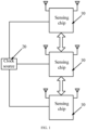
FIG. 1 is a schematic structural view of a cascade solution in the conventional art; -
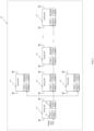
FIG. 2 is a schematic structural view of a sensing system provided according to an embodiment of the present application; -
FIG. 3 is a schematic structural view of a sensing system provided according to another embodiment of the present application; -
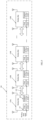
FIG. 4 is a schematic structural view of a sensing system provided according to yet another embodiment of the present application; -
FIG. 5 is a schematic structural view of a sensing system provided according to still another embodiment of the present application; -
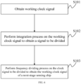
FIG. 6 is a flowchart of a method for obtaining a working clock signal provided according to an embodiment of the present application. - As described in the background technology, in order to improve the angular resolution and maximum detection distance of the sensing system, it is necessary to use multiple sensing chips in a cascading manner. For example, three sensing chips with a single transmitter and a single receiver can be cascaded together to work simultaneously, to achieve the equivalent effect of three transmitters and three receivers. The sensing chip cascade solution in the conventional art is shown in
FIG. 1 , which is based on aclock source 20 to provide working clock signals formultiple sensing chips 10. This scheme can generate stable working clock signals formultiple sensing chips 10 to use together. However, due to the driving ability of thesingle clock source 20, the number ofsensing chips 10 in this cascade solution is greatly limited. The sensing system that simultaneously shares theclock source 20 greatly restricts the placement ofmultiple sensing chips 10 on the printed circuit board (PCB). In addition, the interconnecting wiring betweenmultiple sensing chips 10 becomes more complex and cumbersome, thereby increasing the difficulty of designing and arranging the sensing system. - In view of this, a sensing system is provided according to the embodiments of the present application, the sensing system includes at least one chip branch, and each of the at least one chip branch includes N sensing chips connected sequentially. In the chip branch, the clock circuit of each of the N sensing chips is configured to integrate the received working clock signal, to obtain a stable and relatively high frequency intermediate clock signal. The frequency dividing circuit is configured to divide the clock signal to obtain the working clock signal required for the next-stage sensing chip. In the cascaded structure, the clock source only needs to provide the working clock signal of the first-stage sensing chip, which meets the driving requirements of the first-stage sensing chip. The working clock signal required by other sensing chips is provided by an upper-stage sensing chip, which solves the problem of the number of sensing chips connected in series in the chip branch being limited by the driving ability of the clock source, and expands the applicability of the sensing system.
- Moreover, in the chip branch of the sensing system, the placement and wiring of the connected sequentially sensing chips are not limited by the location of the clock source, which is conducive to improving the design flexibility of the sensing system and simplifying the layout difficulty of the sensing system.
- The following will provide a clear and complete description of the technical solution in the embodiments of the present application in conjunction with the accompanying drawings. Obviously, the described embodiments are only a part of the embodiments of the present application, not all of them. Based on the embodiments in the present application, all other embodiments obtained by ordinary technical personnel in this field without creative labor shall fall within the scope of protection in the present application.
- The present application embodiment provides a sensing system, as shown in
FIG. 2 andFIG. 3 , the sensing system includes at least one chip branch, where each of the at least one chip branch includes N sensing chips connected sequentially to form N cascading stages, and N is an integer greater than one. - Each of the N sensing chips includes a clock circuit and a frequency dividing circuit, the clock circuit is configured to receive an input working clock signal, and to perform an integration process on the input working clock signal to obtain an intermediate clock signal.
- The frequency dividing circuit is configured to receive the intermediate clock signal, and to perform a frequency dividing process on the intermediate clock signal to obtain an output working clock signal. The input working clock signal received by the clock circuit of a first-stage sensing chip comprises a first working clock signal received by the at least one chip branch, the input working clock signal received by the clock circuit of an ith-stage sensing chip is the output working clock signal output by the frequency dividing circuit of an (i-1) th-stage sensing chip, i is an integer greater than one and less or equal to N.
- The
clock circuit 111 and the frequency dividingcircuit 112 are both existing receivers in each of theN sensing chips 110. In onechip branch 100, except for the working clock signal received by the firststage sensing chip 110, which is input from the outside, the working clock signal received by theother sensing chips 110 is provided by the upperstage sensing chip 110. The working clock signal input from the outside can be provided by a clock source such as an oscillator. - The working clock signal received by the
sensing chip 110 is not only provided to theclock circuit 111, but also to other structures of thesensing chip 110 to meet the working requirements of these structures. - In the
sensing chip 110, in response to theclock circuit 111 receiving the working clock signal, it is integrated and processed to improve the driving ability of the working clock signal (by increasing the frequency of the working clock chip, e.g., increasing the working clock signal to 400MHz), and then the frequency dividingcircuit 112 perform the frequency dividing process on the working clock signal to obtain the working clock signal of the required frequency for the next-stage sensing chip 110. - For example, for the
77GHz sensing chip 110, the required working clock signal is 50MHz. Therefore, the frequency dividingcircuit 112 of the upper-stage sensing chip 110 is configured to divide 400MHz eight times, to obtain a 50MHz working clock signal for the77GHz sensing chip 110. For the60GHz sensing chip 110, the required working clock signal is 40MHz. Therefore, the frequency dividingcircuit 112 of the upper-stage sensing chip 110 performs frequency dividing process ten times on 400MHz to obtain a 40MHz working clock signal for the60GHz sensing chip 110. - It should be noted that the phase of the intermediate clock signal output by the
clock circuit 111 generally needs to be the same as the phase of the input working clock signal. Therefore, the phase of the output working clock signal obtained after the intermediate clock signal is divided by the frequency dividingcircuit 112 is also the same as the phase of the input working clock signal. Of course, in response to the phase of the required working clock signal being different between asensing chip 110 and an upper-stage sensing chip 110, the phase of the intermediate clock signal output by theclock circuit 111 can also be different from the phase of the input working clock signal, so that the phase of the output working clock signal obtained after the intermediate clock signal is divided by the frequency dividingcircuit 112 is different from the phase of the input working clock signal, which depends on the actual situation, and is not limited thereto the present application. - In addition, the
clock circuit 111 is configured to output clock signals of other phases as backup in addition to the intermediate clock signal. Correspondingly, in response to dividing the intermediate clock signal, the frequency dividingcircuit 112 not only obtains the working clock signal required by the next-stage sensing chip 110, but also continuously divides the clock signal from one division to M division, to obtain multiple clock signals. Except for outputting the clock signal required by the nextlevel sensing chip 110 as the working clock signal, all other clock signals can be used as backup, and M is a positive integer greater than 1, such as 127. The frequency dividingcircuit 112 is specifically configured to continuously divide the intermediate clock signal from 1 to M to obtain multiple backup clock signals with different frequencies. Based on the clock signal frequency required by the next-stage sensing chip 110, the working clock signal output by the frequency dividingcircuit 112 is determined from the multiple backup clock signals. - In
FIG. 2 , the sensing system includes achip branch 100, and eachchip branch 100 includesN sensing chips 110 connected sequentially. The value of N can be any integer greater than 1, such as 2, 3, 4, 5, 6, etc. The specific value can be determined according to actual needs. - In
FIG. 3 , the sensing system includes threechip branches 100, similarly, each chip cascadedbranch 100 includesN sensing chips 110 connected sequentially. InFIG. 2 andFIG. 3 , the working clock signal received by the firststage sensing chip 110 of eachchip branch 100 is provided by an external clock source of thesensing chip 110, which may be an oscillator or the like, which is not limited thereto the present application. - It is not difficult to understand that
FIG. 2 andFIG. 3 show the case where there are one and threechip branches 100, respectively. In other embodiments of the present application, the number ofchip branches 100 in the sensing system may be 2, 4, 5, etc. However, it should be noted that the number ofchip branches 100 still needs to be limited by the driving ability of the clock source, as the number ofchip branches 100 increases, the firststage sensing chip 110 of eachchip branch 100 still requires a clock source to provide a working clock signal for driving. - In addition, referring to
FIG. 4 , in an optional embodiment of the present application, in one of thechip branches 100, the number of jth-stage sensing chips 110 may not only be 1, may also be 2, 3, 4, etc., which depends on the driving ability of the working clock signal output by thesensing chip 110 and actual requirements. And, j is a positive integer greater than 1, which can further expand the number ofsensing chips 110 that can be cascaded in eachchip branch 100 of the sensing system, and further expand the applicability of the sensing system. - For the type of
sensing chip 110 in the sensing system or thechip branch 100, optionally, in an embodiment of the present application, the type ofsensing chip 110 in thechip branch 100 is the same. For example, they may all be asensing chip 110 with a single transmitter and a single receiver, or may all be asensing chip 110 with two transmitters and two receivers, or may all be asensing chip 110 with a single transmitter and two receivers. - In the
sensing chip 110, the working clock signal output by thefrequency dividing circuit 112 and the working clock signal received by theclock circuit 111 are homologous clock signals. - Due to the same type of
sensing chips 110 in the cascadedbranch 100 in the sensing system, the working clock signals received and output by eachsensing chip 110 are all homologous clock signals to meet the working requirements of eachsensing chip 110. Homologous clock signals refer to clock signals with the same frequency and phase. In addition, in thesensing chip 110, theclock circuits 111 is configured to output the same clock signals to be divided, the phase of the intermediate clock signal is the same as the phase of the input working clock signal, and the frequency of the working clock signal output by the dividingcircuit 112 is the same as the frequency of the working clock signal input to thesensing chip 110, which can ensure that the working clock signal output by the next-stage sensing chip 110 under thesensing chip 110 and the working clock signal received by thesensing chip 110 are homologous clock signals. - Optionally, in another embodiment of the present application, the
chip branch 100 includes at least two types ofsensing chips 110. Thechip branch 100 includes at least two types ofsensing chips 110, such as asensing chip 110 with a single transmitter and a single receiver, or asensing chip 110 with two transmitters and two receivers, or asensing chip 110 with a single transmitter and two receivers. - In response to there being two types of
sensing chips 110 included in thechip branch 100, theclock circuits 111 of eachsensing chip 110 is configured to output the same or different clock signals to be divided. Optionally, in an embodiment of the present application, thechip branch 100 includes two types ofsensing chips 110, and the first stage sensing chip and the secondstage sensing chip 110 are both sensingchips 110 with a single transmitter and a single receiver, The third-stage sensing chip 110 is asensing chip 110 with two transmitters and two receivers, which is optional. The working clock signal received by the firstlevel sensing chip 110 and the output working clock signal are homologous clock signals to meet the working requirements of the same type of secondlevel sensing chip 110. The second-stage sensing chip 110 is designed to meet the working requirements of the third-stage sensing chip 110 with different types. The frequency and/or phase of the working clock signal output by the secondstage sensing chip 110 to the thirdstage sensing chip 110 may be different from the working clock signal received by the secondstage sensing chip 110. Therefore, in response to at least two types ofsensing chips 110 being included in thechip branch 100, theclock circuit 111 of eachsensing chip 110 is configured to output the same or different clock signals to be divided. - For the specific structure of the
clock circuit 111, optionally, theclock circuit 111 includes a phase-locked loop, which can obtain stable and high-frequency clock signals after the working clock signal is integrated. Specifically, the phase-locked loop is configured to receive the working clock signal, process the working clock signal, and generate four phase clock signals. One of the four phase clock signals with the same phase as the working clock signal in the four phase clock signals is used as the intermediate clock signal, and the other three phase clock signals are used as backup clock signals. - Optionally, as an intermediate node, the sensing chip (or integrated circuit) serves as an intermediate node can be reused as the already integrated phase-locked loop of the main body to achieve clock synchronization between each sensing chip, or a phase-locked loop can be additionally set to achieve clock synchronization between each sensing chip, which can be set according to actual needs.
- In addition, in response to a phase-locked loop being separately arranged to achieve clock synchronization between various sensing chips, the sensing chips at the end nodes of each cascaded branch do not need to output a reference clock for the next-stage sensing chip, and there is also no need to arrange a phase-locked loop structure and/or frequency dividing circuit for clock synchronization.
- Moreover, for any sensing chip or integrated circuit provided with a clock circuit and a frequency dividing circuit, in the sensing chip or the integrated circuit, the clock circuit and frequency dividing circuit can be integrated into a phase-locked loop, that is, the frequency dividing circuit can be a frequency divider in the phase-locked loop, or a phase-locked loop can be used as a clock circuit, and a frequency divider can be used as the above frequency dividing circuit. That is, there is a frequency divider in the phase-locked loop that is used to implement the function of the phase-locked loop, while a frequency divider arranged outside the phase-locked loop can be used to divide the output of the phase-locked loop to obtain the output working clock signal.
- In an optional embodiment, the phase-locked loop in the traditional sensing chip can be reused as the clock circuit, and a frequency divider can be added to receive the output of the reused phase-locked loop for frequency dividing to obtain the working clock of the next level sensing chip.
- The phase difference between the four phase clock signals obtained by the phase-locked loop after the working clock signal is processed is 90 degrees. Generally, the phase of the working clock signals required by a
sensing chip 110 and an upperstage sensing chip 110 is the same. Therefore, the phase-locked loop takes the one phase clock signal in the four phase clock signals that has the same phase as the working clock signal as the intermediate clock signal. - On the basis of the above embodiments, in an embodiment of the present application, referring to
FIG. 5 , thechip branch 100 includesN sensing chips 110 including onemaster sensing chip 110A and at least oneslave sensing chip 110B. - The
master sensing chip 110A is configured to control the working status of each of the at least oneslave sensing chip 110B, and themaster sensing chip 110A is further configured to collect radar signals received by the at least oneslave sensing chip 110B, summarize and process the radar signals, and transmit the processed radar signals outward. - Optionally, for the control function of the
master sensing chip 110A on the at least oneslave sensing chip 110B, themaster sensing chip 110A is further configured to receive an enable signal, generate a control signal based on the enable signal, and transmit the control signal to the next-stageslave sensing chip 110B through thedata channel 120. - Each of the at least one
slave sensing chip 110B is further configured to receive the control signal, operate according to the control signal, and transmit the control signal to the next-stageslave sensing chip 110B through thedata channel 120. - In an optional embodiment, the
sensing chip 110 provided in the present application embodiment further includes a digital function module and an operation control device. The digital function module is communicatively connected to the operation control device, theclock circuit 111, and thefrequency dividing circuit 112, respectively. - The digital function module is configured to detect whether the
clock circuit 111 and thefrequency dividing circuit 112 are abnormal or not, and the operation control device is configured to control the digital function module to operate. - Specifically, the each of the N sensing chips 110 includes a digital circuit, a digital function module and an operation control device. The
clock circuit 111 and thefrequency dividing circuit 112 are part of the digital circuit. Various digital circuits are the basic structure of thesensing chip 110. Different digital circuits can realize different functions of thesensing chip 110. The digital function module is configured to detect whether each digital circuit works normally or not. The operation control device is configured to perform unified configuration management on the digital function module. The digital controller in the operation control device is configured to send control signals for function detection to the digital function module through the digital control interface. The configuration module is configured to store configuration information and status information, which can be obtained externally. The state machine is configured to control the workflow of each of thesensing chips 110, and read the configuration information stored in the configuration module, generate corresponding control signals for the control digital controller, and output the control signals to the digital function module to detect various digital circuits by the control digital function module. - The
above sensing chip 110 uses a unified digital controller to connect to the digital function modules of the on-chip system through a digital control interface. After that, the configuration module and the state machine are used to achieve unified configuration management of the operation states of the digital function modules in the on-chip system, thereby improving the operational control efficiency of the on-chip system in thesensing chip 110. - Optionally, in an embodiment, the
above sensing chip 110 is a millimeterwave sensing chip 110. - The frequency of the intermediate clock signal is greater than the frequency of the working clock signal. The types of digital function modules in the
sensing chip 110 can be determined based on actual needs. For example, in the millimeterwave sensing chip 110, the digital function module may be a power detector, etc., which can be used to detect whether the voltage value of the antenna power amplifier is abnormal or not, and the operation control device can control the operation of the power detector. - Correspondingly, a method for obtaining a working clock signal is further provided according to the embodiments of the present application, which is implemented based on the sensing system described in any of the above embodiments. The sensing system includes at least one
chip branch 100 includingN sensing chips 110 connected sequentially, with N greater than one, as shown inFIG. 6 . The method for obtaining the working clock signal includes: - In operation S101, the working clock signal is obtained. The working clock signal received by the
clock circuit 111 of the firststage sensing chip 110 includes an external working clock signal. The working clock signal received by theclock circuit 111 of the ith-stage sensing chip 110 is the working clock signal output by thefrequency dividing circuit 112 of the i-1th-stage sensing chip 110, with i greater than 2. - In operation S102, the intermediate clock signal is obtained by performing an integration process on the working clock signal.
- In operation S103, the output working clock signal is obtained by performing a frequency dividing processing on the intermediate clock signal.
- In an embodiment, an integrated circuit for forming a cascaded branch is provided according to the present application, and the integrated circuit includes a clock circuit and a frequency dividing circuit.
- The clock circuit is configured to receive an input working clock signal, and to perform an integration process on the working clock signal to obtain an intermediate clock signal.
- The frequency dividing circuit is configured to receive the intermediate clock signal, and to perform a frequency dividing process on the intermediate clock signal to obtain an output working clock signal.
- The integrated circuit generally includes a digital circuit, a digital function module and an operation control device. The digital function module is communicatively connected to the digital circuit, respectively. The digital function module is configured to detect whether the digital circuit is abnormal or not, and the operation control device is configured to control the digital function module to operate.
- In the integrated circuit, various digital circuits are the basic structure of the integrated circuit. The clock circuit and the frequency dividing circuit are both digital circuits. Different digital circuits can realize different functions of the integrated circuit (i.e., sensing chip 110). The digital function module is configured to detect whether each digital circuit works normally or not. The operation control device is configured to perform unified configuration management on the digital function module. The digital controller in the operation control device is configured to send control signals for function detection to the digital function module through the digital control interface. The configuration module is configured to store configuration information and status information, which can be obtained externally. The state machine is configured to control the workflow of each of the
sensing chips 110, and read the configuration information stored in the configuration module, generate corresponding control signals for the control digital controller, and output the control signals to the digital function module to detect various digital circuits by the control digital function module. - The above integrated circuit adopts a unified digital controller to connect with the digital function module of the system on chip through a digital control interface. After that, the configuration module and the state machine are configured to achieve unified configuration management of the operation states of the digital function module in the system on chip, thereby improving the efficiency of the operation control of the system on chip in the integrated circuit.
- The types of digital function modules in integrated circuits can be determined based on actual needs, such as power detectors, which can be configured to detect whether the voltage value of the antenna power amplifier is abnormal, and the operation control device is configured to control the operation of the power detector.
- Optionally, the working clock signal received by the clock circuit of the first stage integrated circuit in the cascaded branch includes an external working clock signal.
- The working clock signal received by the clock circuit of the ith-stage integrated circuit is the working clock signal output by the frequency dividing circuit of the i-lth-stage integrated circuit. Among them, i is an integer greater than one.
- Optionally, the frequency dividing circuit is further configured to receive the intermediate clock signal, perform frequency dividing processing on the clock signal to obtain at least one frequency dividing clock signal for the integrated circuit to transmit and receive signals and/or signal processing and/or data processing.
- Optionally, the integrated circuit includes a phase-locked loop, and the clock circuit and/or the frequency dividing circuit are integrated into the phase-locked loop.
- It should be noted that the integrated circuit can integrate a phase-locked loop structure for its normal operation, and the phase-locked loop structure includes the clock circuit and/or frequency dividing circuit mentioned in the above embodiments of the present application. In addition, the phase-locked loop structure can also be used as the clock circuit mentioned above, and a frequency dividing circuit can be added for frequency dividing processing of the intermediate clock signal output by the phase-locked loop structure. In addition, the clock circuit and the frequency dividing circuit can also be added to obtain the clock signal of the next stage integrated circuit, and the clock circuit and frequency dividing circuit can be two separate circuit modules, or can be an integrated circuit module with signal integration and frequency dividing processing, such as another added phase-locked loop structure.
- Optionally, the integrated circuit is an AiP structure and/or an AoC structure.
- In an optional embodiment, the integrated circuit can be equivalent to the sensing chip described in any above embodiment of the present application, that is, the integrated circuit can have the same structure and function with the sensing chip, or can be combined with each other to form a cascade structure. For the sake of simplicity, it will not be repeated here, but it should be understood that technical solutions can be known by those of skills in the art based on the content recorded in the present application shall fall within the scope of the present application.
- In an embodiment, a radio device is further provided according to the embodiments of the present application, the radio device includes a carrier, a sensing system or an integrated circuit, where the sensing system is the sensing system according to any one of above embodiments, the integrated circuit is the integrated circuit according to any one of above embodiments, and the sensing system includes
sensing chips 110 arranged on the carrier. The radio device further includes an antenna, and the antenna is arranged on the carrier or integrated with the sensing chip or the integrated circuit to be arranged on the carrier (i.e., the antenna may be the antenna arranged in the AiP structure or the AoC structure). The sensing chips 110 or the integrated circuit is connected to the antenna (i.e., thesensing chips 110 or the integrated circuit is not provided with any antenna, such as SoC). Among them, the carrier is a PCB, and the first transmission line is PCB wiring. - In an embodiment, a device is further provided according to the present application, and the device includes a device main body, and a radio device, where the radio device is the radio device according to any one of above embodiments, and is arranged on the device main body. The radio device is configured to perform object detection and/or communication.
- Specifically, on the basis of the above embodiments, in an embodiment of the present application, the radio device is arranged outside the device main body. In another embodiment of the present application, the radio device is arranged inside the device main body. In other embodiments of the present application, the radio device may also be partially arranged inside the device main body and partially arranged outside the device main body, which will not be limited there to the present application, and may vary depending on the circumstances.
- It should be noted that radio components can achieve functions such as target detection and communication by transmitting and receiving signals.
- In an optional embodiment, the above device main body may be a component and a product applied in fields such as smart houses, transportation, smart homes, consumer electronics, monitoring, industrial automation, cabin detection, and healthcare. For example, the device main body may be an intelligent transportation device (e.g., a car, a bicycle, a motorcycle, a ship, a subway, a trains, etc.), a security device (e.g., a camera), a liquid level/flow rate detection device, an intelligent wearable device (e.g., a bracelet, a pair of glasses, etc.), a smart home device (e.g., a television, an air conditioner, a smart light, etc.), various communication devices (e.g., mobile phones, tablets, etc.), as well as devices such as road gates, intelligent traffic indicator lights, Intelligent signs, traffic cameras, and various industrial robotic arms (or robots) can also be used as various instruments for detecting vital feature parameters, as well as various devices equipped with such instruments. The radio device is the radio device described in any embodiment of the present application. The structure and working principle of the radio device have been detailed in the above embodiments, and will not be elaborated here.
- In summary, the embodiments of the present application provide a sensing system, a method for obtaining a working clock signal, an integrated circuit, and a radio device. The sensing system includes at least one
chip branch 100, and each of the at least onechip branch 100 includesN sensing chips 110 connected sequentially. In thechip branch 100, theclock circuit 111 of each of the N sensing chips 110 is configured to integrate the received working clock signal, to obtain a stable and relatively high frequency intermediate clock signal. Thefrequency dividing circuit 112 is configured to divide the clock signal to obtain the working clock signal required for the next-stage sensing chip 110. In the cascaded structure, the clock source only needs to provide the working clock signal of the first-stage sensing chip 110, which meets the driving requirements of the first-stage sensing chip 110. The working clock signal required byother sensing chips 110 is provided by an upper-stage sensing chip 110, which solves the problem of the number ofsensing chips 110 connected in series in the chip branch being limited by the driving ability of the clock source, and expands the applicability of the sensing system. - Moreover, in the
chip branch 100 of the sensing system, the placement and wiring of the connected sequentially sensingchips 110 are not limited by the location of the clock source, which is beneficial for improving the design flexibility of the sensing system and simplifying the difficulty of the sensor system layout.
Claims (13)
- A sensing system comprising:at least one chip branch (100), wherein each of the at least one chip branch (100) comprises N sensing chips (110) connected sequentially to form N cascading stages, N being an integer greater than one;characterized in thateach of the N sensing chips (110) comprises a clock circuit (111) and a frequency dividing circuit (112), the clock circuit (111) is configured to receive an input working clock signal, and to perform an integration process on the input working clock signal by increasing its frequency to obtain an intermediate clock signal;the frequency dividing circuit (112) is configured to receive the intermediate clock signal, and to perform a frequency dividing process on the intermediate clock signal to obtain an output working clock signal for a next-stage sensing chip (110);the input working clock signal received by the clock circuit (111) of a first-stage sensing chip (110) comprises a first working clock signal received by the at least one chip branch (100), the input working clock signal received by the clock circuit (111) of an ith-stage sensing chip (110) is the output working clock signal output by the frequency dividing circuit (112) of an (i-1) th-stage sensing chip (110), i being an integer greater than one and less or equal to N; andeach of the at least one chip branch (100) comprises at least two types of sensing chips (110), and the clock circuit (111) of one respective sensing chip (110) of the N sensing chips (110) is configured to output an intermediate clock signal same as or different from an intermediate clock signal output by the clock circuit (111) of another respective sensing chip (110) of the N sensing chips (110).
- The sensing system according to claim 1, wherein each of the at least one chip branch (100) comprises one type of sensing chips (110); and
in each of the N sensing chips (110), the output working clock signal output by the frequency dividing circuit (112) and the input working clock signal received by the clock circuit (111) are homologous clock signals. - The sensing system according to claim 1, wherein in each of the at least one chip branch (100), a number of a jth-stage sensing chip (110) is greater than or equal to 1.
- The sensing system according to claim 1, wherein the clock circuit (111) comprises a phase-locked loop.
- The sensing system according to claim 4, wherein the phase-locked loop is configured to receive the input working clock signal, process the input working clock signal to generate four phase clock signals, determine one of the four phase clock signals with a same phase as the input working clock signal as the intermediate clock signal, and determine remaining three of the four phase clock signals as backup clock signals.
- The sensing system according to claim 1, wherein the frequency dividing circuit (112) is configured to continuously divide the intermediate clock signal from 1 to M to obtain multiple backup clocks with different frequencies, and determine the output working clock signal output by the frequency dividing circuit (112) from multiple backup clocks based on the clock signal frequency required by the next-stage sensing chip (110), M being an integer greater than 1.
- The sensing system according to claim 1, wherein the N sensing chips (110) of each of the at least one chip branch (100) comprises one master sensing chip (110A) and at least one slave sensing chip (110B).
- The sensing system according to claim 7, wherein the master sensing chip (110A) is configured to receive an enable signal, generate a control signal based on the enable signal, and transmit the control signal to a next-stage slave sensing chip (110B) through a data channel (120); and
wherein each of the at least one slave sensing chip (110B) is configured to receive the control signal, operate based on the control signal, and transmit the control signal to the next-stage slave sensing chip (110B) through the data channel (120). - The sensing system according to claim 1, wherein each of the N sensing chips (110) further comprises: a digital function module and an operation control device, the digital function module is communicatively connected to the operation control device, the clock circuit (111), and the frequency dividing circuit (112), respectively; and
the digital function module is configured to detect whether the clock circuit (111) and the frequency dividing circuit (112) are abnormal or not, and the operation control device is configured to control the digital function module to operate. - The sensing system according to any one of claims 1 to 9, wherein each of the N sensing chips (110) is a millimeter wave sensing chip (110); and/or the intermediate clock signal has greater frequency than the working clock signal.
- A method for obtaining a working clock signal, implemented by the sensing system according to any one of claims 1 to 10, the sensing system comprises at least one chip branch (100), wherein the at least one chip branch (100) comprises N sensing chips (110) connected sequentially, N being greater than one, and the method for obtaining the working clock signal comprises:obtaining (S101) a working clock signal;performing (S102) an integration process on the working clock signal by increasing its frequency to obtain an intermediate clock signal; andperforming (S103) a frequency dividing process on the intermediate clock signal to obtain an output working clock signal for a next-stage sensing chip.
- An integrated circuit, characterized by comprising a clock circuit (111) and a frequency dividing circuit (112);wherein the clock circuit (111) is configured to receive a working clock signal, and to perform an integration process on the working clock signal by increasing its frequency to obtain an intermediate clock signal;the frequency dividing circuit (112) is configured to receive the intermediate clock signal, and to perform frequency dividing process on the intermediate clock signal to obtain an output working clock signal;the integrated circuit is configured to form a stage in a cascaded branch including N cascading stages connected sequentially, N being an integer greater than one;the input working clock signal received by the clock circuit (111) is a first working clock signal received by the cascaded branch when the integrated circuit forms a first-stage of the N cascading stages;the input working clock signal received by the clock circuit (111) is an output working clock signal output by an (i-1) th-stage when the integrated circuit forms an ith stage of the N cascading stages, i being an integer greater than one and less or equal to N; and wherein the integrated circuit is a sensing chip (110).
- The integrated circuit according to claim 12, wherein the working clock signal received by the clock circuit (111) of a first stage of the integrated circuit in the cascaded branch comprises an external working clock signal; anda working clock signal received by the clock circuit (111) of an ith-stage of the integrated circuit is the working clock signal output by the frequency dividing circuit (112) of an (i-1)th-stage of the integrated circuit, with i being greater than one;optionally, the frequency dividing circuit (112) is further configured to receive the intermediate clock signal, and obtain at least one frequency dividing clock signal for the integrated circuit to transmit and receive signals and/or signal processing and/or data processing after the intermediate clock signal is divided in frequency.
Applications Claiming Priority (1)
| Application Number | Priority Date | Filing Date | Title |
|---|---|---|---|
| PCT/CN2021/082306 WO2022198434A1 (en) | 2021-03-23 | 2021-03-23 | Sensing system, related apparatus, and method for obtaining working clock signal |
Publications (4)
| Publication Number | Publication Date |
|---|---|
| EP4318952A1 EP4318952A1 (en) | 2024-02-07 |
| EP4318952A4 EP4318952A4 (en) | 2024-06-05 |
| EP4318952B1 true EP4318952B1 (en) | 2025-05-14 |
| EP4318952B8 EP4318952B8 (en) | 2025-07-16 |
Family
ID=83396170
Family Applications (1)
| Application Number | Title | Priority Date | Filing Date |
|---|---|---|---|
| EP21932066.0A Active EP4318952B8 (en) | 2021-03-23 | 2021-03-23 | Sensing system, related apparatus, and method for obtaining working clock signal |
Country Status (2)
| Country | Link |
|---|---|
| EP (1) | EP4318952B8 (en) |
| WO (1) | WO2022198434A1 (en) |
Family Cites Families (9)
| Publication number | Priority date | Publication date | Assignee | Title |
|---|---|---|---|---|
| US6204713B1 (en) * | 1999-01-04 | 2001-03-20 | International Business Machines Corporation | Method and apparatus for routing low-skew clock networks |
| US8766681B2 (en) * | 2012-09-07 | 2014-07-01 | Applied Micro Circuits Corporation | Device and method for a multiplexor/demultiplexor reset scheme |
| DE102015218542A1 (en) * | 2015-09-28 | 2017-03-30 | Robert Bosch Gmbh | Integrated high-frequency circuit, radar sensor and operating method |
| CN106992770B (en) * | 2016-01-21 | 2021-03-30 | 华为技术有限公司 | Clock circuit and method for transmitting clock signal |
| CN106776426B (en) * | 2016-12-05 | 2020-10-27 | 清华大学 | Transmitter with time sequence calibration |
| DE102017217805B4 (en) * | 2017-10-06 | 2019-05-02 | Vega Grieshaber Kg | Radar level gauge with synchronization signal on different line types |
| US11171655B2 (en) * | 2019-06-27 | 2021-11-09 | Intel Corporation | Multi-chip synchronization with applications in multiple-input multiple-output (MIMO) radar systems |
| CN110958018A (en) * | 2019-12-19 | 2020-04-03 | 中船重工(武汉)凌久电子有限责任公司 | A Design Method for Generating Multi-Frequency Synchronous Clock Systems |
| CN113055000B (en) * | 2021-03-23 | 2023-08-11 | 加特兰微电子科技(上海)有限公司 | Sensing system, related device and method for acquiring working clock signal |
-
2021
- 2021-03-23 WO PCT/CN2021/082306 patent/WO2022198434A1/en not_active Ceased
- 2021-03-23 EP EP21932066.0A patent/EP4318952B8/en active Active
Also Published As
| Publication number | Publication date |
|---|---|
| EP4318952B8 (en) | 2025-07-16 |
| EP4318952A4 (en) | 2024-06-05 |
| WO2022198434A1 (en) | 2022-09-29 |
| EP4318952A1 (en) | 2024-02-07 |
Similar Documents
| Publication | Publication Date | Title |
|---|---|---|
| CN113055000B (en) | Sensing system, related device and method for acquiring working clock signal | |
| JP6650512B2 (en) | High frequency integrated circuit, radar sensor and operating method | |
| CN107577626A (en) | A kind of synchronous data collection device based on the Big Dipper, method and system | |
| CN104579455A (en) | Multi-data-channel automatic selection type processing device of satellite-borne data transmission transmitter | |
| CN108134645A (en) | Radar signal synchronization system | |
| US20160259745A1 (en) | High frequency apparatus and method for controlling high frequency apparatus | |
| US12500731B2 (en) | Sensing system, method for obtaining working clock signal, integrated circuit, radio device, and device | |
| EP4318952A1 (en) | Sensing system, related apparatus, and method for obtaining working clock signal | |
| CN111367161B (en) | A remote timing system for observation instruments | |
| US20120033772A1 (en) | Synchroniser circuit and method | |
| CN114401483A (en) | Portable converged communication base station based on high-precision positioning and positioning system | |
| CN117707285A (en) | Automatic switching system for internal and external reference clocks for high-speed signal processing | |
| CN103888132A (en) | Circuit and method for generating two paths of I/Q orthogonal clocks | |
| CN211577426U (en) | A radar circuit, radar and device | |
| CN211044503U (en) | Mobile monitor based on Bluetooth Mesh | |
| CN217789650U (en) | Low-cost high-precision clock driving circuit | |
| US8243614B2 (en) | Hardware efficient monitoring of input/output signals | |
| CN112816984A (en) | Radar circuit, radar and equipment | |
| CN208796235U (en) | A kind of multi-path signal pickup assembly and signal handling equipment | |
| US20260082190A1 (en) | Parallel input/output expansion device for equipment | |
| CN218298521U (en) | Radar system for measurement | |
| RU2219586C2 (en) | Automated work station of air traffic control operator | |
| CN121232113A (en) | A cascaded system, sensor and terminal device | |
| CN223006440U (en) | Chip module and electronic equipment | |
| CN219287537U (en) | Clock synchronization device and mobile terminal |
Legal Events
| Date | Code | Title | Description |
|---|---|---|---|
| STAA | Information on the status of an ep patent application or granted ep patent |
Free format text: STATUS: THE INTERNATIONAL PUBLICATION HAS BEEN MADE |
|
| PUAI | Public reference made under article 153(3) epc to a published international application that has entered the european phase |
Free format text: ORIGINAL CODE: 0009012 |
|
| STAA | Information on the status of an ep patent application or granted ep patent |
Free format text: STATUS: REQUEST FOR EXAMINATION WAS MADE |
|
| 17P | Request for examination filed |
Effective date: 20231019 |
|
| AK | Designated contracting states |
Kind code of ref document: A1 Designated state(s): AL AT BE BG CH CY CZ DE DK EE ES FI FR GB GR HR HU IE IS IT LI LT LU LV MC MK MT NL NO PL PT RO RS SE SI SK SM TR |
|
| REG | Reference to a national code |
Ref country code: DE Ref country code: DE Ref legal event code: R079 Ref document number: 602021030964 Country of ref document: DE Free format text: PREVIOUS MAIN CLASS: H03L0007099000 Ipc: G01S0013870000 |
|
| A4 | Supplementary search report drawn up and despatched |
Effective date: 20240507 |
|
| RIC1 | Information provided on ipc code assigned before grant |
Ipc: H03L 7/06 20060101ALN20240430BHEP Ipc: G06F 1/14 20060101ALI20240430BHEP Ipc: G01S 7/02 20060101ALI20240430BHEP Ipc: G06F 1/10 20060101ALI20240430BHEP Ipc: G01S 13/87 20060101AFI20240430BHEP |
|
| DAV | Request for validation of the european patent (deleted) | ||
| DAX | Request for extension of the european patent (deleted) | ||
| GRAP | Despatch of communication of intention to grant a patent |
Free format text: ORIGINAL CODE: EPIDOSNIGR1 |
|
| STAA | Information on the status of an ep patent application or granted ep patent |
Free format text: STATUS: GRANT OF PATENT IS INTENDED |
|
| RIC1 | Information provided on ipc code assigned before grant |
Ipc: H03L 7/06 20060101ALN20250116BHEP Ipc: G06F 1/14 20060101ALI20250116BHEP Ipc: G01S 7/02 20060101ALI20250116BHEP Ipc: G06F 1/10 20060101ALI20250116BHEP Ipc: G01S 13/87 20060101AFI20250116BHEP |
|
| INTG | Intention to grant announced |
Effective date: 20250130 |
|
| GRAS | Grant fee paid |
Free format text: ORIGINAL CODE: EPIDOSNIGR3 |
|
| GRAA | (expected) grant |
Free format text: ORIGINAL CODE: 0009210 |
|
| STAA | Information on the status of an ep patent application or granted ep patent |
Free format text: STATUS: THE PATENT HAS BEEN GRANTED |
|
| AK | Designated contracting states |
Kind code of ref document: B1 Designated state(s): AL AT BE BG CH CY CZ DE DK EE ES FI FR GB GR HR HU IE IS IT LI LT LU LV MC MK MT NL NO PL PT RO RS SE SI SK SM TR |
|
| REG | Reference to a national code |
Ref country code: GB Ref legal event code: FG4D |
|
| REG | Reference to a national code |
Ref country code: CH Ref legal event code: EP |
|
| REG | Reference to a national code |
Ref country code: DE Ref legal event code: R096 Ref document number: 602021030964 Country of ref document: DE |
|
| REG | Reference to a national code |
Ref country code: IE Ref legal event code: FG4D |
|
| GRAT | Correction requested after decision to grant or after decision to maintain patent in amended form |
Free format text: ORIGINAL CODE: EPIDOSNCDEC |
|
| REG | Reference to a national code |
Ref country code: CH Ref legal event code: PK Free format text: BERICHTIGUNG B8 |
|
| RAP4 | Party data changed (patent owner data changed or rights of a patent transferred) |
Owner name: CALTERAH SEMICONDUCTOR TECHNOLOGY (SHANGHAI)CO., LTD. |
|
| REG | Reference to a national code |
Ref country code: CH Ref legal event code: PK Free format text: BERICHTIGUNG B8 |
|
| REG | Reference to a national code |
Ref country code: NL Ref legal event code: MP Effective date: 20250514 |
|
| PG25 | Lapsed in a contracting state [announced via postgrant information from national office to epo] |
Ref country code: ES Free format text: LAPSE BECAUSE OF FAILURE TO SUBMIT A TRANSLATION OF THE DESCRIPTION OR TO PAY THE FEE WITHIN THE PRESCRIBED TIME-LIMIT Effective date: 20250514 Ref country code: FI Free format text: LAPSE BECAUSE OF FAILURE TO SUBMIT A TRANSLATION OF THE DESCRIPTION OR TO PAY THE FEE WITHIN THE PRESCRIBED TIME-LIMIT Effective date: 20250514 Ref country code: PT Free format text: LAPSE BECAUSE OF FAILURE TO SUBMIT A TRANSLATION OF THE DESCRIPTION OR TO PAY THE FEE WITHIN THE PRESCRIBED TIME-LIMIT Effective date: 20250915 |
|
| REG | Reference to a national code |
Ref country code: LT Ref legal event code: MG9D |
|
| PG25 | Lapsed in a contracting state [announced via postgrant information from national office to epo] |
Ref country code: NO Free format text: LAPSE BECAUSE OF FAILURE TO SUBMIT A TRANSLATION OF THE DESCRIPTION OR TO PAY THE FEE WITHIN THE PRESCRIBED TIME-LIMIT Effective date: 20250814 Ref country code: GR Free format text: LAPSE BECAUSE OF FAILURE TO SUBMIT A TRANSLATION OF THE DESCRIPTION OR TO PAY THE FEE WITHIN THE PRESCRIBED TIME-LIMIT Effective date: 20250815 |
|
| PG25 | Lapsed in a contracting state [announced via postgrant information from national office to epo] |
Ref country code: NL Free format text: LAPSE BECAUSE OF FAILURE TO SUBMIT A TRANSLATION OF THE DESCRIPTION OR TO PAY THE FEE WITHIN THE PRESCRIBED TIME-LIMIT Effective date: 20250514 Ref country code: PL Free format text: LAPSE BECAUSE OF FAILURE TO SUBMIT A TRANSLATION OF THE DESCRIPTION OR TO PAY THE FEE WITHIN THE PRESCRIBED TIME-LIMIT Effective date: 20250514 |
|
| REG | Reference to a national code |
Ref country code: AT Ref legal event code: MK05 Ref document number: 1795229 Country of ref document: AT Kind code of ref document: T Effective date: 20250514 |
|
| PG25 | Lapsed in a contracting state [announced via postgrant information from national office to epo] |
Ref country code: BG Free format text: LAPSE BECAUSE OF FAILURE TO SUBMIT A TRANSLATION OF THE DESCRIPTION OR TO PAY THE FEE WITHIN THE PRESCRIBED TIME-LIMIT Effective date: 20250514 |
|
| PG25 | Lapsed in a contracting state [announced via postgrant information from national office to epo] |
Ref country code: HR Free format text: LAPSE BECAUSE OF FAILURE TO SUBMIT A TRANSLATION OF THE DESCRIPTION OR TO PAY THE FEE WITHIN THE PRESCRIBED TIME-LIMIT Effective date: 20250514 |
|
| PG25 | Lapsed in a contracting state [announced via postgrant information from national office to epo] |
Ref country code: AT Free format text: LAPSE BECAUSE OF FAILURE TO SUBMIT A TRANSLATION OF THE DESCRIPTION OR TO PAY THE FEE WITHIN THE PRESCRIBED TIME-LIMIT Effective date: 20250514 |
|
| PG25 | Lapsed in a contracting state [announced via postgrant information from national office to epo] |
Ref country code: RS Free format text: LAPSE BECAUSE OF FAILURE TO SUBMIT A TRANSLATION OF THE DESCRIPTION OR TO PAY THE FEE WITHIN THE PRESCRIBED TIME-LIMIT Effective date: 20250814 |
|
| PG25 | Lapsed in a contracting state [announced via postgrant information from national office to epo] |
Ref country code: IS Free format text: LAPSE BECAUSE OF FAILURE TO SUBMIT A TRANSLATION OF THE DESCRIPTION OR TO PAY THE FEE WITHIN THE PRESCRIBED TIME-LIMIT Effective date: 20250914 |
|
| PG25 | Lapsed in a contracting state [announced via postgrant information from national office to epo] |
Ref country code: LV Free format text: LAPSE BECAUSE OF FAILURE TO SUBMIT A TRANSLATION OF THE DESCRIPTION OR TO PAY THE FEE WITHIN THE PRESCRIBED TIME-LIMIT Effective date: 20250514 |
|
| PG25 | Lapsed in a contracting state [announced via postgrant information from national office to epo] |
Ref country code: SM Free format text: LAPSE BECAUSE OF FAILURE TO SUBMIT A TRANSLATION OF THE DESCRIPTION OR TO PAY THE FEE WITHIN THE PRESCRIBED TIME-LIMIT Effective date: 20250514 Ref country code: DK Free format text: LAPSE BECAUSE OF FAILURE TO SUBMIT A TRANSLATION OF THE DESCRIPTION OR TO PAY THE FEE WITHIN THE PRESCRIBED TIME-LIMIT Effective date: 20250514 |
|
| PG25 | Lapsed in a contracting state [announced via postgrant information from national office to epo] |
Ref country code: CZ Free format text: LAPSE BECAUSE OF FAILURE TO SUBMIT A TRANSLATION OF THE DESCRIPTION OR TO PAY THE FEE WITHIN THE PRESCRIBED TIME-LIMIT Effective date: 20250514 |
|
| PG25 | Lapsed in a contracting state [announced via postgrant information from national office to epo] |
Ref country code: SK Free format text: LAPSE BECAUSE OF FAILURE TO SUBMIT A TRANSLATION OF THE DESCRIPTION OR TO PAY THE FEE WITHIN THE PRESCRIBED TIME-LIMIT Effective date: 20250514 |
|
| PG25 | Lapsed in a contracting state [announced via postgrant information from national office to epo] |
Ref country code: IT Free format text: LAPSE BECAUSE OF FAILURE TO SUBMIT A TRANSLATION OF THE DESCRIPTION OR TO PAY THE FEE WITHIN THE PRESCRIBED TIME-LIMIT Effective date: 20250514 |
|
| REG | Reference to a national code |
Ref country code: DE Ref legal event code: R097 Ref document number: 602021030964 Country of ref document: DE |
|
| PLBE | No opposition filed within time limit |
Free format text: ORIGINAL CODE: 0009261 |
|
| STAA | Information on the status of an ep patent application or granted ep patent |
Free format text: STATUS: NO OPPOSITION FILED WITHIN TIME LIMIT |
|
| REG | Reference to a national code |
Ref country code: CH Ref legal event code: L10 Free format text: ST27 STATUS EVENT CODE: U-0-0-L10-L00 (AS PROVIDED BY THE NATIONAL OFFICE) Effective date: 20260325 |
|
| PGFP | Annual fee paid to national office [announced via postgrant information from national office to epo] |
Ref country code: GB Payment date: 20260209 Year of fee payment: 6 |
|
| PGFP | Annual fee paid to national office [announced via postgrant information from national office to epo] |
Ref country code: DE Payment date: 20260320 Year of fee payment: 6 |
|
| PGFP | Annual fee paid to national office [announced via postgrant information from national office to epo] |
Ref country code: FR Payment date: 20260209 Year of fee payment: 6 |
|
| 26N | No opposition filed |
Effective date: 20260217 |