EP4317765A1 - Light source apparatus, and electronic apparatus - Google Patents
Light source apparatus, and electronic apparatus Download PDFInfo
- Publication number
- EP4317765A1 EP4317765A1 EP22779613.3A EP22779613A EP4317765A1 EP 4317765 A1 EP4317765 A1 EP 4317765A1 EP 22779613 A EP22779613 A EP 22779613A EP 4317765 A1 EP4317765 A1 EP 4317765A1
- Authority
- EP
- European Patent Office
- Prior art keywords
- light
- light source
- source device
- incident
- optical system
- Prior art date
- Legal status (The legal status is an assumption and is not a legal conclusion. Google has not performed a legal analysis and makes no representation as to the accuracy of the status listed.)
- Pending
Links
Images





Classifications
-
- G—PHYSICS
- G02—OPTICS
- G02B—OPTICAL ELEMENTS, SYSTEMS OR APPARATUS
- G02B27/00—Optical systems or apparatus not provided for by any of the groups G02B1/00 - G02B26/00, G02B30/00
- G02B27/01—Head-up displays
- G02B27/0101—Head-up displays characterised by optical features
-
- G—PHYSICS
- G02—OPTICS
- G02B—OPTICAL ELEMENTS, SYSTEMS OR APPARATUS
- G02B19/00—Condensers, e.g. light collectors or similar non-imaging optics
- G02B19/0033—Condensers, e.g. light collectors or similar non-imaging optics characterised by the use
- G02B19/0047—Condensers, e.g. light collectors or similar non-imaging optics characterised by the use for use with a light source
- G02B19/0061—Condensers, e.g. light collectors or similar non-imaging optics characterised by the use for use with a light source the light source comprising a LED
-
- B—PERFORMING OPERATIONS; TRANSPORTING
- B60—VEHICLES IN GENERAL
- B60K—ARRANGEMENT OR MOUNTING OF PROPULSION UNITS OR OF TRANSMISSIONS IN VEHICLES; ARRANGEMENT OR MOUNTING OF PLURAL DIVERSE PRIME-MOVERS IN VEHICLES; AUXILIARY DRIVES FOR VEHICLES; INSTRUMENTATION OR DASHBOARDS FOR VEHICLES; ARRANGEMENTS IN CONNECTION WITH COOLING, AIR INTAKE, GAS EXHAUST OR FUEL SUPPLY OF PROPULSION UNITS IN VEHICLES
- B60K35/00—Instruments specially adapted for vehicles; Arrangement of instruments in or on vehicles
- B60K35/10—Input arrangements, i.e. from user to vehicle, associated with vehicle functions or specially adapted therefor
-
- B—PERFORMING OPERATIONS; TRANSPORTING
- B60—VEHICLES IN GENERAL
- B60K—ARRANGEMENT OR MOUNTING OF PROPULSION UNITS OR OF TRANSMISSIONS IN VEHICLES; ARRANGEMENT OR MOUNTING OF PLURAL DIVERSE PRIME-MOVERS IN VEHICLES; AUXILIARY DRIVES FOR VEHICLES; INSTRUMENTATION OR DASHBOARDS FOR VEHICLES; ARRANGEMENTS IN CONNECTION WITH COOLING, AIR INTAKE, GAS EXHAUST OR FUEL SUPPLY OF PROPULSION UNITS IN VEHICLES
- B60K35/00—Instruments specially adapted for vehicles; Arrangement of instruments in or on vehicles
- B60K35/20—Output arrangements, i.e. from vehicle to user, associated with vehicle functions or specially adapted therefor
- B60K35/21—Output arrangements, i.e. from vehicle to user, associated with vehicle functions or specially adapted therefor using visual output, e.g. blinking lights or matrix displays
- B60K35/23—Head-up displays [HUD]
-
- B—PERFORMING OPERATIONS; TRANSPORTING
- B60—VEHICLES IN GENERAL
- B60K—ARRANGEMENT OR MOUNTING OF PROPULSION UNITS OR OF TRANSMISSIONS IN VEHICLES; ARRANGEMENT OR MOUNTING OF PLURAL DIVERSE PRIME-MOVERS IN VEHICLES; AUXILIARY DRIVES FOR VEHICLES; INSTRUMENTATION OR DASHBOARDS FOR VEHICLES; ARRANGEMENTS IN CONNECTION WITH COOLING, AIR INTAKE, GAS EXHAUST OR FUEL SUPPLY OF PROPULSION UNITS IN VEHICLES
- B60K35/00—Instruments specially adapted for vehicles; Arrangement of instruments in or on vehicles
- B60K35/20—Output arrangements, i.e. from vehicle to user, associated with vehicle functions or specially adapted therefor
- B60K35/21—Output arrangements, i.e. from vehicle to user, associated with vehicle functions or specially adapted therefor using visual output, e.g. blinking lights or matrix displays
- B60K35/23—Head-up displays [HUD]
- B60K35/231—Head-up displays [HUD] characterised by their arrangement or structure for integration into vehicles
-
- B—PERFORMING OPERATIONS; TRANSPORTING
- B60—VEHICLES IN GENERAL
- B60K—ARRANGEMENT OR MOUNTING OF PROPULSION UNITS OR OF TRANSMISSIONS IN VEHICLES; ARRANGEMENT OR MOUNTING OF PLURAL DIVERSE PRIME-MOVERS IN VEHICLES; AUXILIARY DRIVES FOR VEHICLES; INSTRUMENTATION OR DASHBOARDS FOR VEHICLES; ARRANGEMENTS IN CONNECTION WITH COOLING, AIR INTAKE, GAS EXHAUST OR FUEL SUPPLY OF PROPULSION UNITS IN VEHICLES
- B60K35/00—Instruments specially adapted for vehicles; Arrangement of instruments in or on vehicles
- B60K35/60—Instruments characterised by their location or relative disposition in or on vehicles
-
- F—MECHANICAL ENGINEERING; LIGHTING; HEATING; WEAPONS; BLASTING
- F21—LIGHTING
- F21S—NON-PORTABLE LIGHTING DEVICES; SYSTEMS THEREOF; VEHICLE LIGHTING DEVICES SPECIALLY ADAPTED FOR VEHICLE EXTERIORS
- F21S2/00—Systems of lighting devices, not provided for in main groups F21S4/00 - F21S10/00 or F21S19/00, e.g. of modular construction
-
- F—MECHANICAL ENGINEERING; LIGHTING; HEATING; WEAPONS; BLASTING
- F21—LIGHTING
- F21V—FUNCTIONAL FEATURES OR DETAILS OF LIGHTING DEVICES OR SYSTEMS THEREOF; STRUCTURAL COMBINATIONS OF LIGHTING DEVICES WITH OTHER ARTICLES, NOT OTHERWISE PROVIDED FOR
- F21V9/00—Elements for modifying spectral properties, polarisation or intensity of the light emitted, e.g. filters
- F21V9/30—Elements containing photoluminescent material distinct from or spaced from the light source
- F21V9/32—Elements containing photoluminescent material distinct from or spaced from the light source characterised by the arrangement of the photoluminescent material
-
- G—PHYSICS
- G02—OPTICS
- G02B—OPTICAL ELEMENTS, SYSTEMS OR APPARATUS
- G02B5/00—Optical elements other than lenses
- G02B5/20—Filters
- G02B5/26—Reflecting filters
-
- G—PHYSICS
- G02—OPTICS
- G02B—OPTICAL ELEMENTS, SYSTEMS OR APPARATUS
- G02B5/00—Optical elements other than lenses
- G02B5/30—Polarising elements
- G02B5/3025—Polarisers, i.e. arrangements capable of producing a definite output polarisation state from an unpolarised input state
- G02B5/3066—Polarisers, i.e. arrangements capable of producing a definite output polarisation state from an unpolarised input state involving the reflection of light at a particular angle of incidence, e.g. Brewster's angle
-
- G—PHYSICS
- G03—PHOTOGRAPHY; CINEMATOGRAPHY; ANALOGOUS TECHNIQUES USING WAVES OTHER THAN OPTICAL WAVES; ELECTROGRAPHY; HOLOGRAPHY
- G03B—APPARATUS OR ARRANGEMENTS FOR TAKING PHOTOGRAPHS OR FOR PROJECTING OR VIEWING THEM; APPARATUS OR ARRANGEMENTS EMPLOYING ANALOGOUS TECHNIQUES USING WAVES OTHER THAN OPTICAL WAVES; ACCESSORIES THEREFOR
- G03B21/00—Projectors or projection-type viewers; Accessories therefor
- G03B21/14—Details
- G03B21/20—Lamp housings
- G03B21/2006—Lamp housings characterised by the light source
- G03B21/2033—LED or laser light sources
- G03B21/204—LED or laser light sources using secondary light emission, e.g. luminescence or fluorescence
-
- G—PHYSICS
- G03—PHOTOGRAPHY; CINEMATOGRAPHY; ANALOGOUS TECHNIQUES USING WAVES OTHER THAN OPTICAL WAVES; ELECTROGRAPHY; HOLOGRAPHY
- G03B—APPARATUS OR ARRANGEMENTS FOR TAKING PHOTOGRAPHS OR FOR PROJECTING OR VIEWING THEM; APPARATUS OR ARRANGEMENTS EMPLOYING ANALOGOUS TECHNIQUES USING WAVES OTHER THAN OPTICAL WAVES; ACCESSORIES THEREFOR
- G03B21/00—Projectors or projection-type viewers; Accessories therefor
- G03B21/14—Details
- G03B21/20—Lamp housings
- G03B21/208—Homogenising, shaping of the illumination light
-
- B—PERFORMING OPERATIONS; TRANSPORTING
- B60—VEHICLES IN GENERAL
- B60K—ARRANGEMENT OR MOUNTING OF PROPULSION UNITS OR OF TRANSMISSIONS IN VEHICLES; ARRANGEMENT OR MOUNTING OF PLURAL DIVERSE PRIME-MOVERS IN VEHICLES; AUXILIARY DRIVES FOR VEHICLES; INSTRUMENTATION OR DASHBOARDS FOR VEHICLES; ARRANGEMENTS IN CONNECTION WITH COOLING, AIR INTAKE, GAS EXHAUST OR FUEL SUPPLY OF PROPULSION UNITS IN VEHICLES
- B60K2360/00—Indexing scheme associated with groups B60K35/00 or B60K37/00 relating to details of instruments or dashboards
- B60K2360/20—Optical features of instruments
- B60K2360/23—Optical features of instruments using reflectors
-
- B—PERFORMING OPERATIONS; TRANSPORTING
- B60—VEHICLES IN GENERAL
- B60K—ARRANGEMENT OR MOUNTING OF PROPULSION UNITS OR OF TRANSMISSIONS IN VEHICLES; ARRANGEMENT OR MOUNTING OF PLURAL DIVERSE PRIME-MOVERS IN VEHICLES; AUXILIARY DRIVES FOR VEHICLES; INSTRUMENTATION OR DASHBOARDS FOR VEHICLES; ARRANGEMENTS IN CONNECTION WITH COOLING, AIR INTAKE, GAS EXHAUST OR FUEL SUPPLY OF PROPULSION UNITS IN VEHICLES
- B60K2360/00—Indexing scheme associated with groups B60K35/00 or B60K37/00 relating to details of instruments or dashboards
- B60K2360/20—Optical features of instruments
- B60K2360/33—Illumination features
- B60K2360/332—Light emitting diodes
-
- B—PERFORMING OPERATIONS; TRANSPORTING
- B60—VEHICLES IN GENERAL
- B60K—ARRANGEMENT OR MOUNTING OF PROPULSION UNITS OR OF TRANSMISSIONS IN VEHICLES; ARRANGEMENT OR MOUNTING OF PLURAL DIVERSE PRIME-MOVERS IN VEHICLES; AUXILIARY DRIVES FOR VEHICLES; INSTRUMENTATION OR DASHBOARDS FOR VEHICLES; ARRANGEMENTS IN CONNECTION WITH COOLING, AIR INTAKE, GAS EXHAUST OR FUEL SUPPLY OF PROPULSION UNITS IN VEHICLES
- B60K2360/00—Indexing scheme associated with groups B60K35/00 or B60K37/00 relating to details of instruments or dashboards
- B60K2360/20—Optical features of instruments
- B60K2360/33—Illumination features
- B60K2360/334—Projection means
-
- B—PERFORMING OPERATIONS; TRANSPORTING
- B60—VEHICLES IN GENERAL
- B60K—ARRANGEMENT OR MOUNTING OF PROPULSION UNITS OR OF TRANSMISSIONS IN VEHICLES; ARRANGEMENT OR MOUNTING OF PLURAL DIVERSE PRIME-MOVERS IN VEHICLES; AUXILIARY DRIVES FOR VEHICLES; INSTRUMENTATION OR DASHBOARDS FOR VEHICLES; ARRANGEMENTS IN CONNECTION WITH COOLING, AIR INTAKE, GAS EXHAUST OR FUEL SUPPLY OF PROPULSION UNITS IN VEHICLES
- B60K2360/00—Indexing scheme associated with groups B60K35/00 or B60K37/00 relating to details of instruments or dashboards
- B60K2360/20—Optical features of instruments
- B60K2360/33—Illumination features
- B60K2360/336—Light guides
-
- G—PHYSICS
- G02—OPTICS
- G02B—OPTICAL ELEMENTS, SYSTEMS OR APPARATUS
- G02B27/00—Optical systems or apparatus not provided for by any of the groups G02B1/00 - G02B26/00, G02B30/00
- G02B27/01—Head-up displays
-
- G—PHYSICS
- G02—OPTICS
- G02B—OPTICAL ELEMENTS, SYSTEMS OR APPARATUS
- G02B5/00—Optical elements other than lenses
- G02B5/30—Polarising elements
- G02B5/3025—Polarisers, i.e. arrangements capable of producing a definite output polarisation state from an unpolarised input state
Definitions
- the present invention relates to a light source device which can be used as a planar light source, and particularly, to a planar light source device which is suitable for use in an electronic device including an image display device aiming at miniaturization.
- HUD head-up display
- ultra-small projector a light source device which is miniaturized and has high efficiency is desired.
- Patent Document 1 conventionally known by the following Patent Document 1 is a light source device using a light guide in which a predetermined texture is formed on a transparent resin in order to realize a miniaturized and highly efficient light source device.
- a thin high-efficiency light source device can be realized by making light incident from an end portion of the light guide and scattering the incident light by a texture formed on a surface of the light guide.
- Patent Document 1 Japanese Unexamined Patent Application Publication No. H11-224518 A
- a light source device including: a collimating optical system configured to, by using a high-luminance light emitting diode (LED) as a solid-state light source, convert light emitted from the solid-state light source into substantially parallel light; and a light guide configured to cause the light emitted from the collimating optical system to be incident and emit the light in a direction different from an incident direction.
- a reflective film is provided so as to have an optical characteristic of reflecting a part of blue light and ultraviolet light to the LED side on any one of an optical element constituting the collimating optical system and an optical element provided between the collimating optical system and the light guide.
- a polarization conversion element is provided to reflect a part of light emitted from the LED to the LED side by an action of the reflective film, and to align a polarization direction of light emitted from the light guide in one direction.
- the electronic device using the above-described light source device as an image display device includes an HUD and an aerial floating image display apparatus.
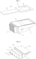
- FIG. 1 is an exploded perspective view illustrating an overview of a light source device according to a first embodiment of the present invention.
- a light source device (main body) 10 is formed of, for example, plastic or the like, and is constituted of a light source device case 11 formed by housing an LED, a collimator, a synthetic diffusion block (diffusion block), a light guide, and the like, which will also be described in detail below, inside the light source device.
- a liquid crystal display element 50 is attached to the upper surface of the light source device, an LED substrate 12 on which a light emitting diode (LED) element which is a semiconductor light source and a control circuit thereof are mounted is attached to one side surface of the light source device, and a heatsink 13 for cooling heat generated in the above-described LED element and control circuit is attached to the outer side surface of the LED substrate 12.
- LED light emitting diode
- the liquid crystal display element 50 attached to the upper surface of the light source device case 11 is constituted of a liquid crystal display panel frame 51, a liquid crystal display panel 52 attached to the frame, and a flexible printed circuit board (FPC) 53 electrically connected to the panel.
- the liquid crystal display panel 52 is controlled by a control signal from a control circuit (not illustrated) constituting the electronic device.
- FIG. 2 illustrates a configuration of an optical system housed inside the light source device 10 described above, that is, in the light source device case 11.
- a plurality of (four in this example) LEDs 14a to 14d (only two LEDs 14a and 14b are illustrated in FIG. 2 ) constituting the light sources are attached to a bottom of each of the LED collimators 15 having a conical convex outer shape obtained by rotating a substantially parabolic disconnection line, and a rectangular synthetic diffusion block 16 is provided on a light emission side of the LED collimators.
- the laser light emitted from the LED 14a or 14b is reflected by a boundary surface of the parabolic line of the LED collimator 15, is converted into parallel light, and is incident on the synthetic diffusion block 16.
- a rod-shaped light guide 17 having a substantially triangular cross section is provided on an emission surface side of the synthetic diffusion block 16 described above via a first diffusion plate 18a, and a second diffusion plate 18b is attached to the upper surface of the light guide.
- horizontal light of the LED collimator 15 described above is reflected upward in the drawing by an action of the light guide 17, and is guided to an incidence surface of the liquid crystal display element 50 described above. Note that, at this point, intensity of the light is uniformized by the first and second diffusion plates 18a and 18b described above.
- a high-output type LED light source is used as the LED light source, and a basic configuration thereof is a configuration in which a phosphor is excited by a blue LED, and a blue excitation light and fluorescent light (including a green component and a red component) are mixed and diverged.
- FIG. 21 is a characteristic diagram illustrating spectral radiant energy of a high-luminance LED for an HUD backlight, which is a Product X of Company A, as a relative value.
- a radiant light flux of 224 to 355 (lm) is output at an input current of 1000 (mA).
- the high-luminance blue LED for exciting a phosphor containing a green component and a red component as output light has a peak wavelength of 440 (nm), a wavelength of 420 (nm) on a short-wavelength side at which luminance is 10% of a peak luminance, and a cutoff wavelength of 360 (nm), and is such that light belonging to a blue short-wavelength region (indicated as a high-energy region in the drawing) from a high-energy ultraviolet region is diverged.
- Other high-luminance LEDs for backlight include, for example, a Product Y of Company B.
- FIG. 23 illustrates a characteristic in which spectral radiant energy is used as a relative value.
- a light flux of 168 (lm) is output at an input current of 650 (mA).
- the high-luminance blue LED for exciting a phosphor containing a green component and a red component as output light has a peak wavelength of 445 (nm), a wavelength of 423 (nm) on the short-wavelength side at which the luminance is 10% of the peak luminance, and the cutoff wavelength of 400 (nm).
- Divergence characteristics of a light source light from the high-luminance LED for the HUD backlight in FIG. 21 are as illustrated in FIG. 22 .
- an LED as a representative example used as a backlight light source for a liquid crystal TV includes, for example, a Product Z of Company B.
- FIG. 25 illustrates a characteristic in which the spectral radiant energy is used as a relative value. A light flux of 168 (lm) is output at an input current of 650 (mA).
- the high-luminance blue LED for exciting a phosphor containing a green component and a red component as output light has a peak wavelength of 450 (nm), a wavelength of 430 (nm) on the short-wavelength side at which the luminance is 10% of the peak luminance, and the cutoff wavelength of 420 (nm), and has characteristics in which the peak wavelength and cutoff wavelength of the high-luminance LED are shifted to a long-wavelength side.
- an optical filter FIL having transmission characteristics illustrated in FIG. 27 is disposed between the LED as the light source and an LCD and the polarizing plate as the image source.
- the filter having a characteristic A obtained by sputtering the metal multilayer film illustrated in FIG. 27 and the filter having a characteristic B obtained by vapor deposition may be provided on a light source light (parallel light) passing surface of an optical element.
- the filter having the characteristic A is provided at a location closer to an LED as a light source, and light in the high-energy region is completely shielded by the filter having the characteristic A.
- the filter having the characteristic B is provided on a light source light passing surface of a different optical element. In order to obtain the filter characteristics described above, it is essential that the light source light is perpendicularly incident on a filter installation surface.
- the divergence characteristics of the light source light from the LED are as illustrated in FIGS. 22 , 24 , and 26 .
- relative luminance is illustrated with a direction perpendicular to an emission surface of the LED (divergence angle of 0 degrees) as 100%.
- the relative luminance is 80%, and at a divergence angle of 60 degrees, the relative luminance is 55% to 50%, and when the LED described above is used as is, the light source light is obliquely incident on the filter installation surface described above.
- the cutoff wavelength is shifted to the short-wavelength side, and affects reliability of the polarizing plate and the LCD panel.
- divergent light from the LED is converted into substantially parallel light by the LED collimator 15, and then the filter FIL having the characteristics illustrated in FIG. 27 is provided on an emission surface 152 of the LED collimator 15 or an incidence surface 162 of the synthetic diffusion block 16, or on both of these surfaces.
- the filter FIL having the characteristics illustrated in FIG. 27 is provided on an emission surface 152 of the LED collimator 15 or an incidence surface 162 of the synthetic diffusion block 16, or on both of these surfaces.
- the divergent light from the LED is converted into substantially parallel light by the LED collimator 15, and then the filter having the characteristics illustrated in FIG. 27 is provided on the emission surface 152, or an incidence surface 214 of a polarization conversion element 21, or on both of these surfaces.
- the high-energy, short-wavelength blue light and ultraviolet light can be cut off, and resistance to the high-luminance light source light can be significantly improved.
- the filter having the characteristic A illustrated in FIG. 27 By providing the filter having the characteristic A illustrated in FIG. 27 on the emission surface 152 of the LED collimator, light (e.g., blue light) in the high-energy region reflected by the filter having the characteristic A excites the phosphor of the high-luminance LED again, so that light output is increased.
- the filter characteristic A illustrated in FIG. 27 is used as a reference (cutoff wavelength of 435 nm)
- the light output is improved by about 15%.
- the cutoff wavelength of 430 (nm) the light output is improved by 12%
- the cutoff wavelength of 420 (nm) the light output is improved by 4%, whereby the light output improvement effect can be confirmed.
- FIG. 3A is a perspective view illustrating the entire light guide 17, the upper part of FIG. 3B includes a cross-sectional view of the light guide, and the lower part of FIG. 3B includes partially enlarged cross-sectional views illustrating the details of the cross sections of the light guide.
- the light guide 17 is, for example, a rod-shaped member having a substantially triangular cross section (see FIG. 3B ) and made of a translucent resin such as acrylic. As illustrated in FIG. 3A , the light guide 17 includes a light guide light incidence portion (surface) 171 configured to face the emission surface of the synthetic diffusion block 16 described above with the first diffusion plate 18a interposed therebetween, a light guide light reflection portion (surface) 172 configured to form an inclined surface, and a light guide light emission portion (surface) 173 configured to face the liquid crystal display panel 52 of the liquid crystal display element 50 described above with the second diffusion plate 18b interposed therebetween.
- a light guide light incidence portion (surface) 171 configured to face the emission surface of the synthetic diffusion block 16 described above with the first diffusion plate 18a interposed therebetween
- a light guide light reflection portion (surface) 172 configured to form an inclined surface
- a light guide light emission portion (surface) 173 configured to face the liquid crystal display panel 52 of the liquid crystal display element 50 described above with the second diffusion plate 18
- each reflection surface 172a (line segment rising to the right in the drawing) forms an angle ⁇ n (n: natural number, e.g., 1 to 130 in this example) with respect to a horizontal plane indicated by the dashed-and-dotted line in the drawing, and ⁇ n is here set to 52 degrees or less (but 44 degrees or more) as an example.
- each connection surface 172b (line segment falling to the right in the drawing) forms an angle of ⁇ n (n: natural number, e.g., 1 to 130 in this example) with respect to the reflection surface 172a.
- the connection surface 172b of the reflection portion is inclined with respect to incident light at an angle at which a shadow is formed within a range of a half-value angle of a scatterer to be described below.
- ⁇ 1, ⁇ 2, ⁇ 3, ⁇ 4... form a reflection surface elevation angle
- ⁇ 1, ⁇ 2, ⁇ 3, ⁇ 4... form a relative angle between the reflection surface and the connection surface, and is set to 90 degrees or more (but 180 degrees or less) as an example.
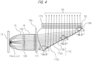
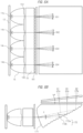
- FIGS. 4 , 5A, and 5B illustrate, for explanatory purposes, schematic diagrams in which the reflection surface 172a and the connection surface 172b are made relatively larger than the light guide 17.
- the main light beam is deflected by ⁇ in a direction in which the incidence angle with respect to the reflection surface 172a increases (see FIG. 5B ).
- the light guide incidence portion (surface) 171 is formed in a curved convex shape inclined toward the light source side.
- the parallel light from the emission surface of the synthetic diffusion block 16 is diffused through the first diffusion plate 18a to be incident, and as is also apparent from the drawing, the incident light reaches the light guide light reflection portion (surface) 172 while being slightly bent (deflected) upward by the light guide incidence portion (surface) 171 (see comparative example of FIG. 6 ).
- the reflection surface elevation angles ⁇ 1, ⁇ 2, ⁇ 3, ⁇ 4... are set such that each reflection surface 172a has an angle larger than or equal to a critical angle with respect to the above-described diffused light, and on the other hand, the relative angles ⁇ 1, ⁇ 2, ⁇ 3, ⁇ 4... between the reflection surface 172a and the connection surface 172b are set to a certain angle as described above, and more preferably are set to an angle of 90 degrees or more ( ⁇ n ⁇ 90°), the reason for which will also be described below.
- each of the reflection surfaces 172a is always formed at an angle larger than or equal to the critical angle with respect to the diffused light, total reflection is possible even if a reflective film made of metal or the like is not formed on the reflection portion 172, and thus, a low-cost light source device can be realized.
- FIG. 6 as a comparative example, when the main light beam is not bent (polarized) at the light guide incidence portion of the light guide 17, a part 31b of the diffused light becomes less than or equal to the critical angle with respect to the reflection surface 172a, making it impossible to secure a sufficient reflectance and to realize a light source device having good (bright) characteristics.
- the reflection surface 172a and the connection surface 172b can be simultaneously machined by an endmill 35 having a relative angle ⁇ between the bottom surface and the side surface in the machining of a mold 40 for manufacturing the light guide 17 by injection-molding. Since the reflection surface 172a and the connection surface 172b can be machined by relatively thick tools, the machining time can be greatly shortened and the machining cost can be greatly reduced. In addition, a boundary edge between the reflection surface 172a and the connection surface 172b can be machined accurately, and light guiding characteristics of the light guide 17 can be improved.
- Lr1, Lr2, Lr3, Lr4... represent projected lengths of the reflection surface 172a with respect to the horizontal plane
- Lc1, Lc2, Lc3, Lc4... represent projected lengths of the connection surface 172b with respect to the horizontal plane
- Lr/Lc, or the ratio between the reflection surface 172a and the connection surface 172b can be changed depending on the location.
- the intensity distribution of the main light beam 30 incident on the light guide 17 does not necessarily coincide with the intensity distribution desired on the incidence surface of the liquid crystal display panel. Therefore, a configuration is adopted in which the intensity distribution is adjusted by the ratio Lr/Lc between the reflection surface 172a and the connection surface 172b.
- the ratio Lr/Lc is set to be different depending on the location in order to correct the light beam, and in particular, the ratio Lr/Lc is set to be small at the center portion. Since the above-described ratio Lr/Lc and the above-described reflection surface elevation angles ⁇ 1, ⁇ 2, ⁇ 3, ⁇ 4... are different depending on the location, an envelope 172c representing a general shape of the reflection portion 172 has a curved shape as illustrated in FIG. 4 .
- the intensity distribution of incident light on the liquid crystal display panel 52 can be made uniform.
- the value of Lr + Lc is smaller than 0.2 mm, not only a long machining time is required, but also it becomes difficult to accurately machine each reflection surface 172a, so that the value is desirably 0.2 mm or more.
- the repetitive structure of the reflection surface 172a requires a certain degree of diffuseness of the diffusion plate 18b because the visibility increases toward the diffusion plate 18b and the uniformity of the light intensity is impaired, but by adopting the present configuration, the repetitive pitch of the reflection surface disposed at a position close to the diffusion plate 18b becomes finer, so that the uniformity of the light intensity can be secured even if the diffuseness of the scattering plate is small, and thus the light utilization efficiency can be improved.
- the value of Lr + Lc is desirably set within the range of 0.2 mm or more and 0.6 mm or less as described above.
- each relative angle ⁇ is set to an angle at which the connection surface 172b is shaded with respect to the light in which the main light beam 30 is diffused by the synthetic diffusion block 16 and the diffusion plate 18a.
- the main light beam incident on the liquid crystal display panel is close to vertical.
- the main light beam can also be inclined by an angle ⁇ .
- some commercially available liquid crystal display panels have better characteristics when the incidence angle is inclined by about 5° to 10°, but in this case, it is desirable to set ⁇ described above to 5° to 10° according to the characteristics.
- FIG. 7 illustrates the synthetic diffusion block 16 integrated with the LED collimator 15 described above
- FIG. 8 illustrates a partially enlarged cross section of the synthetic diffusion block 16.
- a large number of textures 161 having a substantially triangular cross section are formed on the emission surface of the synthetic diffusion block 16, and the light emitted from the LED collimator 15 is diffused in a direction vertical to the plane of the drawing of the incidence portion (surface) 171 of the light guide 17 described above by the action of the textures 161.
- the individual intensity distribution of the light emitted from the emission portion 173 of the light guide 17 can be made uniform.
- a diffusion direction can be limited to the side surface direction of the light guide, and further, the diffuseness in the side surface direction can be controlled by the textures 161, it is possible to weaken the isotropic diffuseness of the first and second diffusion plates 18a and 18b described above, and as a result, the light utilization efficiency is improved, and it is possible to realize a light source device having good characteristics.
- the light utilization efficiency of the laser light from the LED light source and the uniform illumination characteristics thereof can be further improved, and the light source device can be miniaturized and manufactured at low cost, so that in particular, it is possible to provide a light source device suitable as an illumination light source in a display device of an electronic device such as an HUD or an ultra-small projector.
- FIGS. 10 and 11 illustrate a modification example of the light source device according to the first embodiment of the present invention, and as the modification example, an exterior perspective view of an entire light source device 10b and the internal configuration of the light source device are illustrated.
- a plurality of LED collimators 15 each having a conical convex shape to which an LED is attached are attached at an inclined position below the device by using a synthetic diffusion block 16b having a substantially trapezoidal cross section.
- the reference numeral 13b in the drawing denotes a heatsink for cooling heat that is generated in the LED elements and the control circuit.
- FIG. 12 illustrates another modification example of the light source device according to the first embodiment of the present invention, and as another modification example, an exterior perspective view of an entire light source device 10c is illustrated.
- the light source device has a structure in which heat that is generated in an LED substrate 12 is cooled by a heatsink 13c disposed at the lower portion of the device through a heat transfer plate 13d. With the present configuration, a light source device having a short overall length can be realized.
- FIG. 13 illustrates another form of the collimator 15b in the light source device according to the first embodiment of the present invention, and illustrates an example of a shape in which the above-described synthetic diffusion block 16 is combined.
- the collimator shapes illustrated in FIGS. 7 and 8 have external shapes having conical convex shapes obtained by rotating a substantially parabolic disconnection line, but the shapes are based on substantially quadrangular pyramid convex shapes with corners thereof being chamfered or curved.
- the paraboloid of revolution shapes illustrated in FIGS. 7 and 8 are suitable, but the present configuration can realize a more uniform light intensity distribution because the boundaries of the substantially quadrangular pyramid convex shapes are smoothly connected.
- the light source devices 10b and 10c which are modification examples of the light source device of the present invention described above, also have the same action and effect as the light source device 10 illustrated in FIG. 1 described above. Note that, by appropriately selecting these light source devices 10, 10b, and 10c, it is possible to reliably attach the light sources to electronic devices such as an HUD and ultra-small projector having various shapes and forms so as to be adapted to the internal storage spaces of the electronic devices.
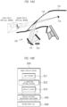
- FIG. 14A illustrates an example in which the light source device described above according to the first embodiment of the present invention is applied to an HUD.
- an image displayed on an image display device 300 including a projector, a liquid crystal display (LCD), or the like is reflected by a mirror 131 or another mirror 132 (e.g., a free-curved surface mirror or a mirror having an optical axis asymmetric shape), and is projected onto a windshield 3 of a vehicle 2.
- a driver 105 sees the image projected onto the windshield 103, thereby visually recognizing the image described above as a virtual image in front of the transparent windshield 103 through the transparent windshield.
- FIG. 14B illustrates an example of the internal configuration of the head-up display device 100 described above, in particular, the image display device 300 thereof.
- the image display device 300 is a projector is illustrated, and the image display device 300 includes, for example, a light source 301, an illumination optical system 302, and a display element 303. Note that, by adopting the above-described light source device 10 of the present invention as the light source 301, it is possible to generate favorable illumination light for projection.
- this example further includes the illumination optical system 302 which is an optical system for condensing illumination light generated by the light source 301, making the illumination light more uniform, and irradiating the display element 303 with the illumination light, and further includes the display element 303 which is an element for generating an image to be projected.
- these elements are already included in the light source device 10 of the present invention as the synthetic diffusion block 16, the first diffusion plate 18a, the light guide 17, and the second diffusion plate 18b, and further as the liquid crystal display panel 52. Therefore, the light source device 10 of the present invention itself can be used as the image display device 300 of the head-up display device 100. According to this, in particular, it is possible to realize the head-up display device 100 which can be easily attached in a narrow space such as a dashboard in an automobile.
- the light emitted from the image display device 300 described above is further projected onto the windshield 103 of a vehicle 102 via a display distance adjustment mechanism 400 and a mirror drive unit 500.
- the light source device 10 of the present invention as an illumination light source of a display device, it is possible to realize an electronic device which can be easily attached even in a narrow space and which is more miniaturized and inexpensive.
- FIGS. 15 to 17B illustrate the configuration of a light source device according to the second embodiment of the present invention, in particular, the configuration of an optical system serving as a feature thereof.
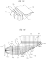
- the number of LEDs 14a and 14b constituting the light sources is two, which is half that of the first embodiment, and the polarization conversion element 21 is provided between the LED collimator 15 for each of the LEDs and the synthetic diffusion block 16.
- the polarization conversion element 21 is provided between the LED collimator 15 for each of the LEDs and the synthetic diffusion block 16.
- the polarization conversion element 21 is configured by combining a columnar (hereinafter referred to as a parallelogram column) translucent member having a parallelogram cross section and a columnar (hereinafter referred to as a triangular column) translucent member having a triangular cross section, which extend along a direction perpendicular to the plane of the drawing, and arranging a plurality of combinations of the members in an array parallel to a plane orthogonal to the optical axis of the parallel light from the LED collimator 15 (in this example, the direction vertical to the plane of the drawing).
- a parallelogram column a columnar (hereinafter referred to as a triangular column) translucent member having a triangular cross section
- PBS polarizing beam splitter
- reflective films 212 are alternately provided at the interface between the adjacent translucent members arranged in an array, and a 1/2 ⁇ phase plate 213 is also provided on the emission surface from which light incident on the polarization conversion element 21 and transmitted through the PBS films 211 is emitted.
- the above-described polarization conversion element 21 is configured symmetrically with respect to the plane (the vertical plane extending vertically on the plane of the drawing) formed by the optical axis of the parallel light from the LED collimator 15 and an extending direction of the translucent member of the parallelogram column, that is, the optical axis plane of the parallel light, and the inclination of the parallelogram column or the triangular column of the translucent member that is a component of the polarization conversion element is 45 degrees with respect to the optical axis plane.
- the polarization conversion elements 21 constitute each of the polarization conversion elements divided into two groups in the vertical direction of the drawing with respect to the parallel light beams from the two LED collimators 15.
- an S-polarized wave (see symbol " ⁇ " in the drawing), for example, of incident light emitted from the LED 14a and converted into parallel light by the LED collimator 15 is reflected by the PBS film 211, and then further reflected by the reflective film 212 to reach an incidence surface of the synthetic diffusion block 16.
- a P-polarized wave (see the up and down arrows in the drawing) is transmitted through the PBS film 211 and then converted into an S-polarized wave by the 1/2 ⁇ phase plate 213 to reach the incidence surface of the synthetic diffusion block 16.
- the polarization conversion element 21 As described above, according to the polarization conversion element 21, all of the light emitted from the (plurality of) LEDs and converted into parallel light by the LED collimator 15 become S-polarized waves and are incident on the incidence surface of the synthetic diffusion block 16. Then, the light emitted from the emission surface of the synthetic diffusion block 16 is made incident on the light guide 17, which is already described above in detail, via the first diffusion plate 18a, and is reflected upward in the drawing by the action of the light guide 17 to be guided to the incidence surface of the above-described liquid crystal display element 50, as in the first embodiment. In other words, the action of the light guide 17 has already been described in detail above, and the description thereof will be omitted here to avoid duplication.
- FIG. 18 is a perspective view illustrating a state in which the two LED collimators 15 described above are attached to the polarization conversion element 21 described above.
- FIG. 19 is a perspective view illustrating the exterior configuration of the synthetic diffusion block 16 attached to the emission surface side of the polarization conversion element
- FIG. 20 is a side view illustrating the detailed structure of the synthetic diffusion block 16 and a partially enlarged cross-sectional view thereof.
- a large number of textures 161 having a substantially triangular cross section are formed on the emission surface of the synthetic diffusion block 16.
- the details thereof have already been described above and will be omitted here.
- the transmittance of the light in the liquid crystal display panel can be improved, so that a more miniaturized and highly efficient light source device can be realized at a lower cost by a smaller number of light emission sources (LEDs).
- LEDs light emission sources
- the liquid crystal display panel has an excellent transmittance for S-polarized waves
- the same action and effect can be obtained by a polarization conversion element having the same configuration as that described above even when the liquid crystal display panel has an excellent transmittance for P-polarized waves.
- the light source device described above according to the second embodiment can also be used as a light source device in an electronic device such as a head-up display device or a projector, as in the light source device described above according to the first embodiment.
- a planar light source device suitable for use in an electronic device including an image display device according to various embodiments of the present invention has been described above.
- the present invention is not limited only to the above-described embodiments, and includes various modification examples.
- the entire system has been described in detail in order to explain the present invention in an easy-to-understand manner, and the present invention is not necessarily limited to a system including all the configurations described above.
- a part of the configuration of a certain embodiment can be replaced with the configuration of another embodiment, and the configuration of another embodiment can be added to the configuration of a certain embodiment.
- a part of the configuration of each embodiment can be added, deleted, or replaced with another configuration.
Landscapes
- Physics & Mathematics (AREA)
- Engineering & Computer Science (AREA)
- General Physics & Mathematics (AREA)
- Optics & Photonics (AREA)
- Transportation (AREA)
- Mechanical Engineering (AREA)
- Chemical & Material Sciences (AREA)
- Combustion & Propulsion (AREA)
- General Engineering & Computer Science (AREA)
- Spectroscopy & Molecular Physics (AREA)
- Multimedia (AREA)
- Planar Illumination Modules (AREA)
- Instrument Panels (AREA)
- Optical Filters (AREA)
- Polarising Elements (AREA)
Abstract
Description
- The present invention relates to a light source device which can be used as a planar light source, and particularly, to a planar light source device which is suitable for use in an electronic device including an image display device aiming at miniaturization.
- As an illumination light source for a display device of a head-up display (hereinafter referred to as "HUD") or an ultra-small projector, a light source device which is miniaturized and has high efficiency is desired.
- Note that conventionally known by the following
Patent Document 1 is a light source device using a light guide in which a predetermined texture is formed on a transparent resin in order to realize a miniaturized and highly efficient light source device. In the light guide illumination device described in this patent document, it is described that a thin high-efficiency light source device can be realized by making light incident from an end portion of the light guide and scattering the incident light by a texture formed on a surface of the light guide. - Patent Document 1:
Japanese Unexamined Patent Application Publication No. H11-224518 A - In recent years, it has been effective to use an LED as a light emitting source of a light source device along with improvement in light emission efficiency of the LED which is a solid-state light source. However, in an optical system using an LED and an LED collimator for converting light from the LED into substantially parallel light, it has been found that the shape of the optical system disclosed in
Patent Document 1 is still insufficient in terms of light utilization efficiency characteristics and uniform illumination characteristics. - Therefore, it is specifically an object of the present invention to provide a light source device which achieves miniaturization of the light source device by further improving light utilization efficiency characteristics and uniform illumination characteristics of laser light from an LED light source, which can be manufactured at low cost, and which is therefore suitable as an illumination light source in a display device of an electronic device such as an HUD or an aerial floating image display apparatus, and to further provide an electronic device including an image display device using the light source device.
- As an embodiment for achieving the above purpose, there is provided a light source device including: a collimating optical system configured to, by using a high-luminance light emitting diode (LED) as a solid-state light source, convert light emitted from the solid-state light source into substantially parallel light; and a light guide configured to cause the light emitted from the collimating optical system to be incident and emit the light in a direction different from an incident direction. A reflective film is provided so as to have an optical characteristic of reflecting a part of blue light and ultraviolet light to the LED side on any one of an optical element constituting the collimating optical system and an optical element provided between the collimating optical system and the light guide. A polarization conversion element is provided to reflect a part of light emitted from the LED to the LED side by an action of the reflective film, and to align a polarization direction of light emitted from the light guide in one direction.
- According to the present invention, the electronic device using the above-described light source device as an image display device includes an HUD and an aerial floating image display apparatus.
- According to the present invention described above, it is possible to realize a light source device that can be manufactured at low cost and that is miniaturized, highly efficient, and highly reliable.
-
-
FIG. 1 is an exploded perspective view illustrating an overall overview of a light source device according to a first embodiment of the present invention. -
FIG. 2 is a perspective view illustrating an overview of an internal configuration of an optical system in the light source device according to the first embodiment of the present invention. -
FIG. 3A is a diagram for explaining details of a light guide in the light source device according to the first embodiment of the present invention. -
FIG. 3B is a diagram for explaining details of the light guide in the light source device according to the first embodiment of the present invention. -
FIG. 4 is a side view describing details of an operation of the light guide in the light source device according to the first embodiment of the present invention. -
FIG. 5A is a top view describing details of the operation of the light guide in the light source device according to the first embodiment of the present invention. -
FIG. 5B is a side view describing details of the operation of the light guide in the light source device according to the first embodiment of the present invention. -
FIG. 6 is a diagram illustrating a comparative example for explaining the operation of the light guide in the light source device according to the first embodiment of the present invention. -
FIG. 7 is a perspective view describing details of a collimator and a synthetic diffusion block in the light source device according to the first embodiment of the present invention. -
FIG. 8 is a partially enlarged cross-sectional view describing details of the synthetic diffusion block in the light source device according to the first embodiment of the present invention. -
FIG. 9 is a diagram describing a method of machining a mold used for molding a light guide which is a component of the optical system of the light source device according to the first embodiment of the present invention. -
FIG. 10 is an exterior perspective view illustrating an overall overview of a light source device which is a modification example of the light source device according to the first embodiment of the present invention. -
FIG. 11 is a perspective view illustrating an overview of an internal configuration of an optical system of a light source device which is a modification example of the light source device according to the first embodiment of the present invention. -
FIG. 12 is an exterior perspective view illustrating an overall overview of a light source device which is another modification example of the light source device according to the first embodiment of the present invention. -
FIG. 13 is a perspective view illustrating another form of the collimator and the shape of the synthetic diffusion block in the light source device according to the first embodiment of the present invention. -
FIG. 14A is a diagram illustrating the configuration of an HUD in which the light source device according to the first embodiment of the present invention is used as an illumination light source of the display device. -
FIG. 14B is a diagram illustrating the configuration of an HUD in which the light source device according to the first embodiment of the present invention is used as an illumination light source of the display device. -
FIG. 15 is a perspective view illustrating an example of a structure of an optical system of a light source device according to a second embodiment of the present invention. -
FIG. 16 is a side view illustrating an operation in the optical system of the light source device according to the second embodiment of the present invention. -
FIG. 17A is a top view describing details of an operation of a light guide in the light source device according to the second embodiment of the present invention. -
FIG. 17B is a side view describing details of the operation of the light guide in the light source device according to the second embodiment of the present invention. -
FIG. 18 is a perspective view illustrating an example of a structure of an LED collimator and a synthetic diffusion block which are components of an optical system of the light source device according to the second embodiment of the present invention. -
FIG. 19 is a perspective view illustrating an example of the structure of the synthetic diffusion block which is a component of the optical system of the light source device according to the second embodiment of the present invention. -
FIG. 20 is a cross-sectional view and partially enlarged cross-sectional views thereof describing details of the synthetic diffusion block in the light source device according to the second embodiment of the present invention. -
FIG. 21 is a characteristic diagram relatively illustrating radiant energy intensity for each wavelength according to a first embodiment of a high-luminance LED light source. -
FIG. 22 is a characteristic diagram relatively illustrating radiant energy divergence intensity according to the first embodiment of the high-luminance LED light source. -
FIG. 23 is a characteristic diagram relatively illustrating radiant energy intensity for each wavelength according to a second embodiment of the high-luminance LED light source. -
FIG. 24 is a characteristic diagram relatively illustrating radiant energy divergence intensity according to the second embodiment of the high-luminance LED light source. -
FIG. 25 is a characteristic diagram relatively illustrating radiant energy intensity for each wavelength of an LED light source for an LCD-TV application. -
FIG. 26 is a characteristic diagram relatively illustrating radiant energy divergence intensity of an LED light source for an LCD-TV application. -
FIG. 27 is a characteristic diagram illustrating spectral transmittance of a filter according to the embodiments. - In the following, embodiments of the present invention will be described in detail with reference to the drawings.
-
FIG. 1 is an exploded perspective view illustrating an overview of a light source device according to a first embodiment of the present invention. As is also apparent from the drawing, a light source device (main body) 10 is formed of, for example, plastic or the like, and is constituted of a lightsource device case 11 formed by housing an LED, a collimator, a synthetic diffusion block (diffusion block), a light guide, and the like, which will also be described in detail below, inside the light source device. A liquidcrystal display element 50 is attached to the upper surface of the light source device, anLED substrate 12 on which a light emitting diode (LED) element which is a semiconductor light source and a control circuit thereof are mounted is attached to one side surface of the light source device, and aheatsink 13 for cooling heat generated in the above-described LED element and control circuit is attached to the outer side surface of theLED substrate 12. - Further, the liquid
crystal display element 50 attached to the upper surface of the lightsource device case 11 is constituted of a liquid crystaldisplay panel frame 51, a liquidcrystal display panel 52 attached to the frame, and a flexible printed circuit board (FPC) 53 electrically connected to the panel. In other words, as will also be described in detail below, the liquidcrystal display panel 52 is controlled by a control signal from a control circuit (not illustrated) constituting the electronic device. -
FIG. 2 illustrates a configuration of an optical system housed inside thelight source device 10 described above, that is, in the lightsource device case 11. - A plurality of (four in this example)
LEDs 14a to 14d (only twoLEDs FIG. 2 ) constituting the light sources are attached to a bottom of each of theLED collimators 15 having a conical convex outer shape obtained by rotating a substantially parabolic disconnection line, and a rectangularsynthetic diffusion block 16 is provided on a light emission side of the LED collimators. In other words, the laser light emitted from theLED LED collimator 15, is converted into parallel light, and is incident on thesynthetic diffusion block 16. - Further, a rod-shaped
light guide 17 having a substantially triangular cross section is provided on an emission surface side of thesynthetic diffusion block 16 described above via afirst diffusion plate 18a, and asecond diffusion plate 18b is attached to the upper surface of the light guide. Thus, horizontal light of theLED collimator 15 described above is reflected upward in the drawing by an action of thelight guide 17, and is guided to an incidence surface of the liquidcrystal display element 50 described above. Note that, at this point, intensity of the light is uniformized by the first andsecond diffusion plates - In the present embodiment, a high-output type LED light source is used as the LED light source, and a basic configuration thereof is a configuration in which a phosphor is excited by a blue LED, and a blue excitation light and fluorescent light (including a green component and a red component) are mixed and diverged.
FIG. 21 is a characteristic diagram illustrating spectral radiant energy of a high-luminance LED for an HUD backlight, which is a Product X of Company A, as a relative value. A radiant light flux of 224 to 355 (lm) is output at an input current of 1000 (mA). The high-luminance blue LED for exciting a phosphor containing a green component and a red component as output light has a peak wavelength of 440 (nm), a wavelength of 420 (nm) on a short-wavelength side at which luminance is 10% of a peak luminance, and a cutoff wavelength of 360 (nm), and is such that light belonging to a blue short-wavelength region (indicated as a high-energy region in the drawing) from a high-energy ultraviolet region is diverged. Other high-luminance LEDs for backlight include, for example, a Product Y of Company B.FIG. 23 illustrates a characteristic in which spectral radiant energy is used as a relative value. A light flux of 168 (lm) is output at an input current of 650 (mA). The high-luminance blue LED for exciting a phosphor containing a green component and a red component as output light has a peak wavelength of 445 (nm), a wavelength of 423 (nm) on the short-wavelength side at which the luminance is 10% of the peak luminance, and the cutoff wavelength of 400 (nm). Divergence characteristics of a light source light from the high-luminance LED for the HUD backlight inFIG. 21 are as illustrated inFIG. 22 . - On the other hand, an LED as a representative example used as a backlight light source for a liquid crystal TV includes, for example, a Product Z of Company B.
FIG. 25 illustrates a characteristic in which the spectral radiant energy is used as a relative value. A light flux of 168 (lm) is output at an input current of 650 (mA). The high-luminance blue LED for exciting a phosphor containing a green component and a red component as output light has a peak wavelength of 450 (nm), a wavelength of 430 (nm) on the short-wavelength side at which the luminance is 10% of the peak luminance, and the cutoff wavelength of 420 (nm), and has characteristics in which the peak wavelength and cutoff wavelength of the high-luminance LED are shifted to a long-wavelength side. - Therefore, in the light source device using the high-luminance LED, it is necessary to limit the amount of blue light (light in the blue region) having high energy which is incident on a liquid crystal panel and a polarizing plate. Therefore, in the present embodiment, for example, an optical filter FIL having transmission characteristics illustrated in
FIG. 27 is disposed between the LED as the light source and an LCD and the polarizing plate as the image source. The filter having a characteristic A obtained by sputtering the metal multilayer film illustrated inFIG. 27 and the filter having a characteristic B obtained by vapor deposition may be provided on a light source light (parallel light) passing surface of an optical element. The filter having the characteristic A is provided at a location closer to an LED as a light source, and light in the high-energy region is completely shielded by the filter having the characteristic A. In addition, it is more preferable that the filter having the characteristic B is provided on a light source light passing surface of a different optical element. In order to obtain the filter characteristics described above, it is essential that the light source light is perpendicularly incident on a filter installation surface. - However, the divergence characteristics of the light source light from the LED are as illustrated in
FIGS. 22 ,24 , and26 . InFIGS. 22 ,24 , and26 , relative luminance is illustrated with a direction perpendicular to an emission surface of the LED (divergence angle of 0 degrees) as 100%. At a divergence angle of 40 degrees, the relative luminance is 80%, and at a divergence angle of 60 degrees, the relative luminance is 55% to 50%, and when the LED described above is used as is, the light source light is obliquely incident on the filter installation surface described above. As a result, the cutoff wavelength is shifted to the short-wavelength side, and affects reliability of the polarizing plate and the LCD panel. - As a countermeasure against the above, in the present embodiment, as illustrated in
FIGS. 4 ,5A, and 5B , divergent light from the LED is converted into substantially parallel light by theLED collimator 15, and then the filter FIL having the characteristics illustrated inFIG. 27 is provided on anemission surface 152 of theLED collimator 15 or anincidence surface 162 of thesynthetic diffusion block 16, or on both of these surfaces. Thus, the high-energy, short-wavelength blue light and ultraviolet light can be cut off, and the resistance to the high-luminance light source light can be improved. - In a second embodiment to be described below, as illustrated in
FIGS. 16 ,17A, and 17B , the divergent light from the LED is converted into substantially parallel light by theLED collimator 15, and then the filter having the characteristics illustrated inFIG. 27 is provided on theemission surface 152, or anincidence surface 214 of apolarization conversion element 21, or on both of these surfaces. Thus, as in the first embodiment, the high-energy, short-wavelength blue light and ultraviolet light can be cut off, and resistance to the high-luminance light source light can be significantly improved. - By providing the filter having the characteristic A illustrated in
FIG. 27 on theemission surface 152 of the LED collimator, light (e.g., blue light) in the high-energy region reflected by the filter having the characteristic A excites the phosphor of the high-luminance LED again, so that light output is increased. When the filter characteristic A illustrated inFIG. 27 is used as a reference (cutoff wavelength of 435 nm), the light output is improved by about 15%. When the cutoff wavelength of 430 (nm) is used, the light output is improved by 12%, and when the cutoff wavelength of 420 (nm) is used, the light output is improved by 4%, whereby the light output improvement effect can be confirmed. - Details of the
light guide 17 constituting thelight source device 10 described above will now be described with reference to the drawings. Note thatFIG. 3A is a perspective view illustrating the entirelight guide 17, the upper part ofFIG. 3B includes a cross-sectional view of the light guide, and the lower part ofFIG. 3B includes partially enlarged cross-sectional views illustrating the details of the cross sections of the light guide. - The
light guide 17 is, for example, a rod-shaped member having a substantially triangular cross section (seeFIG. 3B ) and made of a translucent resin such as acrylic. As illustrated inFIG. 3A , thelight guide 17 includes a light guide light incidence portion (surface) 171 configured to face the emission surface of thesynthetic diffusion block 16 described above with thefirst diffusion plate 18a interposed therebetween, a light guide light reflection portion (surface) 172 configured to form an inclined surface, and a light guide light emission portion (surface) 173 configured to face the liquidcrystal display panel 52 of the liquidcrystal display element 50 described above with thesecond diffusion plate 18b interposed therebetween. - As illustrated in the lower part of
FIG. 3B which includes partially enlarged views thereof, a large number ofreflection surfaces 172a andconnection surfaces 172b are alternately formed in a saw-tooth shape on the light guide light reflection portion (surface) 172 of thelight guide 17. Eachreflection surface 172a (line segment rising to the right in the drawing) forms an angle αn (n: natural number, e.g., 1 to 130 in this example) with respect to a horizontal plane indicated by the dashed-and-dotted line in the drawing, and αn is here set to 52 degrees or less (but 44 degrees or more) as an example. - On the other hand, each
connection surface 172b (line segment falling to the right in the drawing) forms an angle of βn (n: natural number, e.g., 1 to 130 in this example) with respect to thereflection surface 172a. In other words, theconnection surface 172b of the reflection portion is inclined with respect to incident light at an angle at which a shadow is formed within a range of a half-value angle of a scatterer to be described below. As will also be described in detail below, α1, α2, α3, α4... form a reflection surface elevation angle, and β1, β2, β3, β4... form a relative angle between the reflection surface and the connection surface, and is set to 90 degrees or more (but 180 degrees or less) as an example. Note that, in this example, β1 = β2 = β3 = β4 = ... = β122 = ... β130. -
FIGS. 4 ,5A, and 5B illustrate, for explanatory purposes, schematic diagrams in which thereflection surface 172a and theconnection surface 172b are made relatively larger than thelight guide 17. At the light guide incidence portion (surface) 171 of thelight guide 17, the main light beam is deflected by δ in a direction in which the incidence angle with respect to thereflection surface 172a increases (seeFIG. 5B ). In other words, the light guide incidence portion (surface) 171 is formed in a curved convex shape inclined toward the light source side. According to this, the parallel light from the emission surface of thesynthetic diffusion block 16 is diffused through thefirst diffusion plate 18a to be incident, and as is also apparent from the drawing, the incident light reaches the light guide light reflection portion (surface) 172 while being slightly bent (deflected) upward by the light guide incidence portion (surface) 171 (see comparative example ofFIG. 6 ). - Note that a large number of
reflection surfaces 172a andconnection surfaces 172b are alternately formed in a saw-tooth shape on the light guide light reflection portion (surface) 172, and the diffused light is totally reflected on eachreflection surface 172a and directed upward, and further is incident on the liquidcrystal display panel 52 as a parallel diffused light via the light guide light emission portion (surface) 173 and thesecond diffusion plate 18b. Therefore, the reflection surface elevation angles α1, α2, α3, α4... are set such that eachreflection surface 172a has an angle larger than or equal to a critical angle with respect to the above-described diffused light, and on the other hand, the relative angles β1, β2, β3, β4... between thereflection surface 172a and theconnection surface 172b are set to a certain angle as described above, and more preferably are set to an angle of 90 degrees or more (βn ≥ 90°), the reason for which will also be described below. - According to the above-described configuration, since each of the
reflection surfaces 172a is always formed at an angle larger than or equal to the critical angle with respect to the diffused light, total reflection is possible even if a reflective film made of metal or the like is not formed on thereflection portion 172, and thus, a low-cost light source device can be realized. On the other hand, as illustrated inFIG. 6 as a comparative example, when the main light beam is not bent (polarized) at the light guide incidence portion of thelight guide 17, apart 31b of the diffused light becomes less than or equal to the critical angle with respect to thereflection surface 172a, making it impossible to secure a sufficient reflectance and to realize a light source device having good (bright) characteristics. - The reflection surface elevation angles α1, α2, α3, α4... slightly increase from the lower portion to the upper portion of the light guide light reflection portion (surface) 172. Since the light transmitted through the liquid
crystal display panel 52 of the liquidcrystal display element 50 has a certain degree of divergence angle, in order to prevent the so-called peripheral darkening in which a part of the light transmitted through the peripheral portion of the liquidcrystal display panel 52 is blocked by a peripheral edge of a mirror disposed on a downstream side, a configuration is realized such that a peripheral light beam is slightly deflected toward a central axis, as indicated by alight beam 30 inFIG. 4 . - As described above, β1 = β2 = β3 = β4... βn ≥ 90°. This is because, as illustrated in
FIG. 9 , thereflection surface 172a and theconnection surface 172b can be simultaneously machined by anendmill 35 having a relative angle β between the bottom surface and the side surface in the machining of amold 40 for manufacturing thelight guide 17 by injection-molding. Since thereflection surface 172a and theconnection surface 172b can be machined by relatively thick tools, the machining time can be greatly shortened and the machining cost can be greatly reduced. In addition, a boundary edge between thereflection surface 172a and theconnection surface 172b can be machined accurately, and light guiding characteristics of thelight guide 17 can be improved. - In addition, in
FIG. 4 , Lr1, Lr2, Lr3, Lr4... represent projected lengths of thereflection surface 172a with respect to the horizontal plane, Lc1, Lc2, Lc3, Lc4... represent projected lengths of theconnection surface 172b with respect to the horizontal plane, and Lr/Lc, or the ratio between thereflection surface 172a and theconnection surface 172b, can be changed depending on the location. The intensity distribution of themain light beam 30 incident on thelight guide 17 does not necessarily coincide with the intensity distribution desired on the incidence surface of the liquid crystal display panel. Therefore, a configuration is adopted in which the intensity distribution is adjusted by the ratio Lr/Lc between thereflection surface 172a and theconnection surface 172b. Note that, as this ratio is increased, an average intensity of the reflected light at the portion of the surfaces can be increased. In general, since thelight beam 30 incident on the light guide tends to be strong at a center portion, the ratio Lr/Lc is set to be different depending on the location in order to correct the light beam, and in particular, the ratio Lr/Lc is set to be small at the center portion. Since the above-described ratio Lr/Lc and the above-described reflection surface elevation angles α1, α2, α3, α4... are different depending on the location, anenvelope 172c representing a general shape of thereflection portion 172 has a curved shape as illustrated inFIG. 4 . - Further, Lr1 + Lc1 = Lr2 + Lc2 = Lr3 + Lc3 = Lr4 + Lc4... = Lr + Lc ≤ 0.6 mm. By adopting such a configuration, it is possible to make the repetition pitches of the reflection surfaces viewed from a
light emission surface 173 of thelight guide 17 the same. Since the pitch is 0.6 mm or less, in combination with the action and effect of thediffusion plates crystal display panel 52, the individual emission surfaces are not separated and are viewed as a continuous surface, so that the spatial luminance through the liquidcrystal display panel 52 can be made uniform, thereby improving the display characteristics. In other words, with the present configuration, the intensity distribution of incident light on the liquidcrystal display panel 52 can be made uniform. On the other hand, if the value of Lr + Lc is smaller than 0.2 mm, not only a long machining time is required, but also it becomes difficult to accurately machine eachreflection surface 172a, so that the value is desirably 0.2 mm or more. - Further, although not illustrated, the value of Lr + Lc described above (sum of the lengths) may be, in whole or in part, a configuration such that Lr1 + Lc1 > Lr2 + Lc2 > Lr3 + Lc3 > Lr4 + Lc4..., Lr1 + Lc1 = Lr2 + Lc2 = Lr3 + Lc3 = Lr4 + Lc4... = Lr90 + Lc90 > Lr91 + Lc91 = Lr92 + Lc92 > Lr93 + Lc93... > Lr130 + Lc130, or Lr1 + Lc1 ≥ Lr2+ Lc2 > Lr3 + Lc3 ≥ Lr4 + Lc4... Lr1 + Lc1 > Lr130 + Lc130. By adopting such a configuration, the repetition pitch of the
reflection surface 172a viewed from theemission surface 173 of thelight guide 17 becomes finer as the repetition pitch approaches theemission surface 173. Thus, with the present configuration, the repetition pitch of thereflection surface 172a of thelight guide 17 as viewed from thediffusion plate 18b becomes finer as the repetition pitch approaches thediffusion plate 18b. The repetitive structure of thereflection surface 172a requires a certain degree of diffuseness of thediffusion plate 18b because the visibility increases toward thediffusion plate 18b and the uniformity of the light intensity is impaired, but by adopting the present configuration, the repetitive pitch of the reflection surface disposed at a position close to thediffusion plate 18b becomes finer, so that the uniformity of the light intensity can be secured even if the diffuseness of the scattering plate is small, and thus the light utilization efficiency can be improved. Further, the value of Lr + Lc is desirably set within the range of 0.2 mm or more and 0.6 mm or less as described above. - According to the shape of the light guide light reflection portion (surface) 172 of the
light guide 17 described above, the total reflection condition of the main light can be satisfied, a reflection film such as aluminum on thereflection portion 172 need not be provided, light can be reflected efficiently, an operation such as a vapor deposition operation of an aluminum thin film which causes an increase in manufacturing cost need not be performed, and a bright light source can be realized at lower cost. Each relative angle β is set to an angle at which theconnection surface 172b is shaded with respect to the light in which themain light beam 30 is diffused by thesynthetic diffusion block 16 and thediffusion plate 18a. Thus, by suppressing the incidence of unnecessary light on theconnection surface 172b, it is possible to reduce the reflection of unnecessary light, and it is possible to realize a light source device having favorable characteristics. - In general, it is desirable that the inclination of the main light beam incident on the liquid crystal display panel is close to vertical. However, depending on the characteristics of the liquid crystal display panel, as illustrated in
FIG. 5B , the main light beam can also be inclined by an angle η. In other words, some commercially available liquid crystal display panels have better characteristics when the incidence angle is inclined by about 5° to 10°, but in this case, it is desirable to set η described above to 5° to 10° according to the characteristics. - Instead of inclining the panel by η, it is also possible to incline the inclination of the main light beam to the liquid crystal display panel by adjusting the angle of the
reflection surface 172a. Further, if it is necessary to incline the light beam in a side surface direction of the light guide, it can be realized by making the inclination of the slopes oftriangular textures 161 formed on the emission surface of thesynthetic diffusion block 16 asymmetric, or by changing a formation direction of the textures formed by the reflection surfaces 172a and 172b. - The
synthetic diffusion block 16, which is another component of thelight source device 10, will now be described with reference toFIGS. 7 and8 . Note thatFIG. 7 illustrates thesynthetic diffusion block 16 integrated with theLED collimator 15 described above, andFIG. 8 illustrates a partially enlarged cross section of thesynthetic diffusion block 16. - As is also apparent from
FIG. 8 , a large number oftextures 161 having a substantially triangular cross section are formed on the emission surface of thesynthetic diffusion block 16, and the light emitted from theLED collimator 15 is diffused in a direction vertical to the plane of the drawing of the incidence portion (surface) 171 of thelight guide 17 described above by the action of thetextures 161. By the interactions between the above-described substantiallytriangular textures 161 anddiffusion plates LED collimators 15 are discretely disposed, the individual intensity distribution of the light emitted from theemission portion 173 of thelight guide 17 can be made uniform. In particular, since a diffusion direction can be limited to the side surface direction of the light guide, and further, the diffuseness in the side surface direction can be controlled by thetextures 161, it is possible to weaken the isotropic diffuseness of the first andsecond diffusion plates triangular textures 161, the angle γ = 30 degrees and the formation pitch a of the textures = 0.5 mm. - As described above in detail, according to the
light source device 10 of the present invention, the light utilization efficiency of the laser light from the LED light source and the uniform illumination characteristics thereof can be further improved, and the light source device can be miniaturized and manufactured at low cost, so that in particular, it is possible to provide a light source device suitable as an illumination light source in a display device of an electronic device such as an HUD or an ultra-small projector. -
FIGS. 10 and11 illustrate a modification example of the light source device according to the first embodiment of the present invention, and as the modification example, an exterior perspective view of an entirelight source device 10b and the internal configuration of the light source device are illustrated. In this modification example, a plurality ofLED collimators 15 each having a conical convex shape to which an LED is attached are attached at an inclined position below the device by using asynthetic diffusion block 16b having a substantially trapezoidal cross section. Note that thereference numeral 13b in the drawing denotes a heatsink for cooling heat that is generated in the LED elements and the control circuit. - Further,
FIG. 12 illustrates another modification example of the light source device according to the first embodiment of the present invention, and as another modification example, an exterior perspective view of an entirelight source device 10c is illustrated. In this another modification example, although not illustrated in detail, the light source device has a structure in which heat that is generated in anLED substrate 12 is cooled by aheatsink 13c disposed at the lower portion of the device through aheat transfer plate 13d. With the present configuration, a light source device having a short overall length can be realized. - Further,
FIG. 13 illustrates another form of thecollimator 15b in the light source device according to the first embodiment of the present invention, and illustrates an example of a shape in which the above-describedsynthetic diffusion block 16 is combined. The collimator shapes illustrated inFIGS. 7 and8 have external shapes having conical convex shapes obtained by rotating a substantially parabolic disconnection line, but the shapes are based on substantially quadrangular pyramid convex shapes with corners thereof being chamfered or curved. In view of the efficiency of the light emitted from the LED and emitted from thelight guide 17, the paraboloid of revolution shapes illustrated inFIGS. 7 and8 are suitable, but the present configuration can realize a more uniform light intensity distribution because the boundaries of the substantially quadrangular pyramid convex shapes are smoothly connected. - Note that the
light source devices light source device 10 illustrated inFIG. 1 described above. Note that, by appropriately selecting theselight source devices - In addition, an example in which the above-described
light source device 10 of the present invention is mounted on an HUD and an ultra-small projector will be described below as a representative example of an electronic device using the light source device as a light source of the display device thereof. -
FIG. 14A illustrates an example in which the light source device described above according to the first embodiment of the present invention is applied to an HUD. Note that, in this drawing, in a head-updisplay device 100, an image displayed on animage display device 300 including a projector, a liquid crystal display (LCD), or the like is reflected by a mirror 131 or another mirror 132 (e.g., a free-curved surface mirror or a mirror having an optical axis asymmetric shape), and is projected onto a windshield 3 of avehicle 2. On the other hand, adriver 105 sees the image projected onto thewindshield 103, thereby visually recognizing the image described above as a virtual image in front of thetransparent windshield 103 through the transparent windshield. -
FIG. 14B illustrates an example of the internal configuration of the head-updisplay device 100 described above, in particular, theimage display device 300 thereof. As is also apparent from this drawing, a case where theimage display device 300 is a projector is illustrated, and theimage display device 300 includes, for example, alight source 301, an illuminationoptical system 302, and adisplay element 303. Note that, by adopting the above-describedlight source device 10 of the present invention as thelight source 301, it is possible to generate favorable illumination light for projection. - Note that this example further includes the illumination
optical system 302 which is an optical system for condensing illumination light generated by thelight source 301, making the illumination light more uniform, and irradiating thedisplay element 303 with the illumination light, and further includes thedisplay element 303 which is an element for generating an image to be projected. However, in the above-described embodiment, these elements are already included in thelight source device 10 of the present invention as thesynthetic diffusion block 16, thefirst diffusion plate 18a, thelight guide 17, and thesecond diffusion plate 18b, and further as the liquidcrystal display panel 52. Therefore, thelight source device 10 of the present invention itself can be used as theimage display device 300 of the head-updisplay device 100. According to this, in particular, it is possible to realize the head-updisplay device 100 which can be easily attached in a narrow space such as a dashboard in an automobile. - Note that it will be apparent to those skilled in the art that the light emitted from the
image display device 300 described above is further projected onto thewindshield 103 of avehicle 102 via a displaydistance adjustment mechanism 400 and amirror drive unit 500. - As described above in detail, by using the
light source device 10 of the present invention as an illumination light source of a display device, it is possible to realize an electronic device which can be easily attached even in a narrow space and which is more miniaturized and inexpensive. - Details of a second example (second embodiment) of the present invention will now be described. Note that, in the second embodiment, unlike the first embodiment described above, attention is paid to the transmittance with respect to the polarized wave of the liquid
crystal display panel 52 constituting the liquidcrystal display element 50 on which the illumination light from the light source device is incident, and further, a polarization conversion element for aligning a polarization direction of the light emitted from the collimating optical system in one direction is provided, thereby realizing a more miniaturized and highly efficient light source device. -
FIGS. 15 to 17B illustrate the configuration of a light source device according to the second embodiment of the present invention, in particular, the configuration of an optical system serving as a feature thereof. In other words, in the second embodiment, in the configuration of the first embodiment described above, the number ofLEDs polarization conversion element 21 is provided between theLED collimator 15 for each of the LEDs and thesynthetic diffusion block 16. Note that other configurations in the drawings are the same as those of the first embodiment described above, and are denoted by the same reference numerals, and detailed description thereof will be omitted here to avoid duplication. - As is apparent from these drawings, particularly from
FIG. 17A , thepolarization conversion element 21 is configured by combining a columnar (hereinafter referred to as a parallelogram column) translucent member having a parallelogram cross section and a columnar (hereinafter referred to as a triangular column) translucent member having a triangular cross section, which extend along a direction perpendicular to the plane of the drawing, and arranging a plurality of combinations of the members in an array parallel to a plane orthogonal to the optical axis of the parallel light from the LED collimator 15 (in this example, the direction vertical to the plane of the drawing). Further, polarizing beam splitter (hereinafter abbreviated as "PBS")films 211 andreflective films 212 are alternately provided at the interface between the adjacent translucent members arranged in an array, and a 1/2λ phase plate 213 is also provided on the emission surface from which light incident on thepolarization conversion element 21 and transmitted through thePBS films 211 is emitted. - As described above, the above-described
polarization conversion element 21 is configured symmetrically with respect to the plane (the vertical plane extending vertically on the plane of the drawing) formed by the optical axis of the parallel light from theLED collimator 15 and an extending direction of the translucent member of the parallelogram column, that is, the optical axis plane of the parallel light, and the inclination of the parallelogram column or the triangular column of the translucent member that is a component of the polarization conversion element is 45 degrees with respect to the optical axis plane. Thepolarization conversion elements 21 constitute each of the polarization conversion elements divided into two groups in the vertical direction of the drawing with respect to the parallel light beams from the twoLED collimators 15. - According to the
polarization conversion element 21 configured as described above, as illustrated inFIG. 17A , an S-polarized wave (see symbol "×" in the drawing), for example, of incident light emitted from theLED 14a and converted into parallel light by theLED collimator 15 is reflected by thePBS film 211, and then further reflected by thereflective film 212 to reach an incidence surface of thesynthetic diffusion block 16. On the other hand, a P-polarized wave (see the up and down arrows in the drawing) is transmitted through thePBS film 211 and then converted into an S-polarized wave by the 1/2λ phase plate 213 to reach the incidence surface of thesynthetic diffusion block 16. - As described above, according to the
polarization conversion element 21, all of the light emitted from the (plurality of) LEDs and converted into parallel light by theLED collimator 15 become S-polarized waves and are incident on the incidence surface of thesynthetic diffusion block 16. Then, the light emitted from the emission surface of thesynthetic diffusion block 16 is made incident on thelight guide 17, which is already described above in detail, via thefirst diffusion plate 18a, and is reflected upward in the drawing by the action of thelight guide 17 to be guided to the incidence surface of the above-described liquidcrystal display element 50, as in the first embodiment. In other words, the action of thelight guide 17 has already been described in detail above, and the description thereof will be omitted here to avoid duplication. - Note that
FIG. 18 is a perspective view illustrating a state in which the twoLED collimators 15 described above are attached to thepolarization conversion element 21 described above.FIG. 19 is a perspective view illustrating the exterior configuration of thesynthetic diffusion block 16 attached to the emission surface side of the polarization conversion element, andFIG. 20 is a side view illustrating the detailed structure of thesynthetic diffusion block 16 and a partially enlarged cross-sectional view thereof. As is also apparent from these drawings, also in the second embodiment, a large number oftextures 161 having a substantially triangular cross section are formed on the emission surface of thesynthetic diffusion block 16. However, the details thereof have already been described above and will be omitted here. - In other words, according to the light source device described above of the second embodiment, since the light incident on the liquid
crystal display panel 52 constituting the liquidcrystal display element 50 is converted into the S-polarized wave by thepolarization conversion element 21 described above, the transmittance of the light in the liquid crystal display panel can be improved, so that a more miniaturized and highly efficient light source device can be realized at a lower cost by a smaller number of light emission sources (LEDs). Note that, although in the above description, thepolarization conversion element 21 is attached after theLED collimator 15, the present invention is not limited thereto, and it will be apparent to those skilled in the art that the same action and effect can be obtained by providing the polarization conversion element in the optical path leading to the liquid crystal display element. - Further, although it has been described that the liquid crystal display panel has an excellent transmittance for S-polarized waves, it will be apparent to those skilled in the art that the same action and effect can be obtained by a polarization conversion element having the same configuration as that described above even when the liquid crystal display panel has an excellent transmittance for P-polarized waves. It will be apparent to those skilled in the art that the light source device described above according to the second embodiment can also be used as a light source device in an electronic device such as a head-up display device or a projector, as in the light source device described above according to the first embodiment.
- A planar light source device suitable for use in an electronic device including an image display device according to various embodiments of the present invention has been described above. However, the present invention is not limited only to the above-described embodiments, and includes various modification examples. For example, in the above-described embodiments, the entire system has been described in detail in order to explain the present invention in an easy-to-understand manner, and the present invention is not necessarily limited to a system including all the configurations described above. A part of the configuration of a certain embodiment can be replaced with the configuration of another embodiment, and the configuration of another embodiment can be added to the configuration of a certain embodiment. A part of the configuration of each embodiment can be added, deleted, or replaced with another configuration.
-
- 10
- LIGHT SOURCE DEVICE (MAIN BODY)
- 11
- CASE
- 50
- LIQUID CRYSTAL DISPLAY ELEMENT
- 12
- LED SUBSTRATE
- 13
- HEATSINK
- 14a, 14b
- LED
- 15
- LED COLLIMATOR
- 16
- SYNTHETIC DIFFUSION BLOCK
- 17
- LIGHT GUIDE
- 171
- LIGHT GUIDE LIGHT INCIDENCE PORTION (SURFACE)
- 172
- LIGHT GUIDE LIGHT REFLECTION PORTION (SURFACE)
- 172a
- REFLECTION SURFACE
- 172b
- CONNECTION SURFACE
- 173
- LIGHT GUIDE LIGHT EMISSION PORTION (SURFACE)
- 21
- POLARIZATION CONVERSION ELEMENT
- 211
- PBS FILM
- 212
- REFLECTIVE FILM
- 213
- 1/2λ PHASE PLATE
Claims (16)
- A light source device comprising:a light source configured to generate white light by irradiating a phosphor with light emitted from a solid-state light source;a collimating optical system configured to convert a divergent light flux of the white light emitted from the light source into parallel light;a light guide configured to cause the light emitted from the collimating optical system to be incident as incident light and emit the incident light in a direction different from an incident direction; anda filter configured to reflect light in a blue region of the parallel light to irradiate the phosphor.
- The light source device according to claim 1,
wherein the filter is provided on an emission surface of the collimating optical system. - The light source device according to claim 1, comprisinga diffusion block between the collimating optical system and the light guide and configured to diffuse the parallel light,wherein the filter is provided on an incidence surface of the diffusion block.
- The light source device according to claim 3,
wherein the filter is provided on each of an emission surface of the collimating optical system and the incidence surface of the diffusion block. - The light source device according to claim 1,
wherein a divergence angle of a light source emitted from a light source that generates white light by irradiating a phosphor with light emitted from the solid-state light source is 80 degrees or more. - The light source device according to claim 1,
wherein the reflective film has a cutoff wavelength of 435 (nm) or less at which a reflectance is 50%. - The light source device according to claim 1, comprising
a polarization conversion element between the collimating optical system and the light guide and configured to align a polarization direction of light in one direction. - The light source device according to claim 1,wherein the light guide includes an incidence portion on which the incident light is incident, a reflection portion which reflects the incident light, and an emission portion which emits light reflected by the reflection portion, andwherein the reflection portion includes a plurality of reflection surfaces that reflect the incident light and a plurality of connection surfaces that connect the plurality of reflection surfaces, and the incidence portion has a structure that deflects light in a direction in which an incidence angle of the incident light that is incident on the reflection surface of the reflection portion becomes larger.
- The light source device according to claim 7, comprisinga scatterer between the collimating optical system and the light guide,wherein the connection surface is inclined with respect to the incident light at an angle at which a shadow is formed within a range of a half-value angle of the scatterer.
- The light source device according to claim 8,
wherein the incidence surface is an inclined surface disposed obliquely with respect to the incident light. - The light source device according to claim 10,
wherein at least a part of the incidence surface is a curved surface. - The light source device according to claim 9,
wherein an elevation angle of the reflection surface varies depending on a location, and a relative angle between the reflection surface and the connection surface adjacent to each other is 90 degrees or more. - The light source device according to claim 12,
wherein the relative angle is a constant value regardless of location. - The light source device according to claim 12,
wherein an absolute value of an elevation angle of the connection surface is a constant value regardless of location. - The light source device according to claim 8,
wherein a texture structure that diffuses light is formed on an emission surface of the collimating optical system. - An electronic device using the light source device according to claim 1 as an image display device.
Applications Claiming Priority (2)
| Application Number | Priority Date | Filing Date | Title |
|---|---|---|---|
| JP2021055038A JP7534255B2 (en) | 2021-03-29 | 2021-03-29 | Light source device and electronic device |
| PCT/JP2022/006270 WO2022209386A1 (en) | 2021-03-29 | 2022-02-16 | Light source apparatus, and electronic apparatus |
Publications (2)
| Publication Number | Publication Date |
|---|---|
| EP4317765A1 true EP4317765A1 (en) | 2024-02-07 |
| EP4317765A4 EP4317765A4 (en) | 2025-04-09 |
Family
ID=83458829
Family Applications (1)
| Application Number | Title | Priority Date | Filing Date |
|---|---|---|---|
| EP22779613.3A Pending EP4317765A4 (en) | 2021-03-29 | 2022-02-16 | LIGHT SOURCE DEVICE AND ELECTRONIC DEVICE |
Country Status (5)
| Country | Link |
|---|---|
| US (3) | US12050317B2 (en) |
| EP (1) | EP4317765A4 (en) |
| JP (2) | JP7534255B2 (en) |
| CN (1) | CN116868001A (en) |
| WO (1) | WO2022209386A1 (en) |
Families Citing this family (1)
| Publication number | Priority date | Publication date | Assignee | Title |
|---|---|---|---|---|
| KR102851639B1 (en) * | 2022-12-28 | 2025-08-27 | 현대모비스 주식회사 | Picture Generating Apparatus for use in Head-Up Display |
Family Cites Families (13)
| Publication number | Priority date | Publication date | Assignee | Title |
|---|---|---|---|---|
| JPH11224518A (en) | 1997-12-01 | 1999-08-17 | Hiroshi Inoue | Light guide lighting device |
| US20090034230A1 (en) * | 2007-07-31 | 2009-02-05 | Luminus Devices, Inc. | Illumination assembly including wavelength converting material having spatially varying density |
| JP2011107508A (en) * | 2009-11-19 | 2011-06-02 | Showa Denko Kk | Phosphor filter, method of manufacturing the same, and lamp |
| WO2016056285A1 (en) * | 2014-10-10 | 2016-04-14 | ソニー株式会社 | Phosphor wheel, light source apparatus, and projection type display apparatus |
| TWI574098B (en) * | 2015-08-14 | 2017-03-11 | 台達電子工業股份有限公司 | Laser light source for projector |
| WO2017036502A1 (en) * | 2015-08-28 | 2017-03-09 | Coelux S.R.L. | Large area light source and large area luminaire |
| JP6179628B2 (en) * | 2016-03-23 | 2017-08-16 | セイコーエプソン株式会社 | LIGHTING DEVICE, ELECTRONIC DEVICE, AND PROJECTION TYPE DISPLAY DEVICE |
| JP6854590B2 (en) | 2016-04-05 | 2021-04-07 | マクセル株式会社 | Light source device and electronic device using it |
| CN113238315B (en) | 2016-04-05 | 2023-05-12 | 麦克赛尔株式会社 | Light source device and head-up display device |
| JP2017188311A (en) | 2016-04-06 | 2017-10-12 | 日立マクセル株式会社 | Light source device and electronic apparatus using the same |
| JP6783545B2 (en) * | 2016-04-19 | 2020-11-11 | キヤノン株式会社 | Lighting device and projection type display device using it |
| TW201833656A (en) * | 2016-10-12 | 2018-09-16 | 日商索尼股份有限公司 | Image display device and light source device |
| US10520165B1 (en) | 2018-07-09 | 2019-12-31 | Abl Ip Holding Llc | Laser illumination lighting device with solid medium freeform prism or waveguide |
-
2021
- 2021-03-29 JP JP2021055038A patent/JP7534255B2/en active Active
-
2022
- 2022-02-16 EP EP22779613.3A patent/EP4317765A4/en active Pending
- 2022-02-16 US US18/284,568 patent/US12050317B2/en active Active
- 2022-02-16 CN CN202280014593.XA patent/CN116868001A/en active Pending
- 2022-02-16 WO PCT/JP2022/006270 patent/WO2022209386A1/en not_active Ceased
-
2024
- 2024-06-17 US US18/745,119 patent/US12216278B2/en active Active
- 2024-08-01 JP JP2024125672A patent/JP7723157B2/en active Active
- 2024-12-26 US US19/001,713 patent/US20250123485A1/en active Pending
Also Published As
| Publication number | Publication date |
|---|---|
| US12216278B2 (en) | 2025-02-04 |
| WO2022209386A1 (en) | 2022-10-06 |
| JP7723157B2 (en) | 2025-08-13 |
| CN116868001A (en) | 2023-10-10 |
| US20240184108A1 (en) | 2024-06-06 |
| US12050317B2 (en) | 2024-07-30 |
| EP4317765A4 (en) | 2025-04-09 |
| JP2024152743A (en) | 2024-10-25 |
| US20250123485A1 (en) | 2025-04-17 |
| US20240337836A1 (en) | 2024-10-10 |
| JP7534255B2 (en) | 2024-08-14 |
| JP2022152316A (en) | 2022-10-12 |
Similar Documents
| Publication | Publication Date | Title |
|---|---|---|
| CN109073170B (en) | Light source device and electronic device using the same | |
| JP6721453B2 (en) | Head-up display device and its image display device | |
| JP6854590B2 (en) | Light source device and electronic device using it | |
| CN115128814A (en) | Head-up display | |
| CN103370569B (en) | Surface light source device and liquid crystal display device | |
| JP2018060006A (en) | Head-up display device and light source device thereof | |
| US20250123485A1 (en) | Light source device and electronic device | |
| JP2017188311A (en) | Light source device and electronic apparatus using the same | |
| JP7146965B2 (en) | LIGHT SOURCE DEVICE AND ELECTRONIC DEVICE USING THE SAME | |
| JP7324919B2 (en) | vehicle | |
| JP7244556B2 (en) | Light source device and head-up display device | |
| US12066753B2 (en) | Light source apparatus and projector |
Legal Events
| Date | Code | Title | Description |
|---|---|---|---|
| STAA | Information on the status of an ep patent application or granted ep patent |
Free format text: STATUS: THE INTERNATIONAL PUBLICATION HAS BEEN MADE |
|
| PUAI | Public reference made under article 153(3) epc to a published international application that has entered the european phase |
Free format text: ORIGINAL CODE: 0009012 |
|
| STAA | Information on the status of an ep patent application or granted ep patent |
Free format text: STATUS: REQUEST FOR EXAMINATION WAS MADE |
|
| 17P | Request for examination filed |
Effective date: 20230928 |
|
| AK | Designated contracting states |
Kind code of ref document: A1 Designated state(s): AL AT BE BG CH CY CZ DE DK EE ES FI FR GB GR HR HU IE IS IT LI LT LU LV MC MK MT NL NO PL PT RO RS SE SI SK SM TR |
|
| DAV | Request for validation of the european patent (deleted) | ||
| DAX | Request for extension of the european patent (deleted) | ||
| A4 | Supplementary search report drawn up and despatched |
Effective date: 20250311 |
|
| RIC1 | Information provided on ipc code assigned before grant |
Ipc: G02B 5/30 20060101ALN20250305BHEP Ipc: G02B 5/26 20060101ALN20250305BHEP Ipc: B60K 35/60 20240101ALN20250305BHEP Ipc: B60K 35/231 20240101ALN20250305BHEP Ipc: B60K 35/10 20240101ALN20250305BHEP Ipc: G03B 21/20 20060101ALI20250305BHEP Ipc: G02B 27/01 20060101ALI20250305BHEP Ipc: F21V 9/32 20180101ALI20250305BHEP Ipc: F21V 7/28 20180101ALI20250305BHEP Ipc: F21S 2/00 20160101AFI20250305BHEP |