EP4312365A1 - Aging-averse bandwidth extension apparatus - Google Patents
Aging-averse bandwidth extension apparatus Download PDFInfo
- Publication number
- EP4312365A1 EP4312365A1 EP23174288.3A EP23174288A EP4312365A1 EP 4312365 A1 EP4312365 A1 EP 4312365A1 EP 23174288 A EP23174288 A EP 23174288A EP 4312365 A1 EP4312365 A1 EP 4312365A1
- Authority
- EP
- European Patent Office
- Prior art keywords
- circuit
- driver
- inverter
- switch
- node
- Prior art date
- Legal status (The legal status is an assumption and is not a legal conclusion. Google has not performed a legal analysis and makes no representation as to the accuracy of the status listed.)
- Granted
Links
Images







Classifications
-
- H—ELECTRICITY
- H03—ELECTRONIC CIRCUITRY
- H03K—PULSE TECHNIQUE
- H03K19/00—Logic circuits, i.e. having at least two inputs acting on one output; Inverting circuits
- H03K19/003—Modifications for increasing the reliability for protection
- H03K19/00315—Modifications for increasing the reliability for protection in field-effect transistor circuits
-
- H—ELECTRICITY
- H03—ELECTRONIC CIRCUITRY
- H03F—AMPLIFIERS
- H03F1/00—Details of amplifiers with only discharge tubes, only semiconductor devices or only unspecified devices as amplifying elements
- H03F1/42—Modifications of amplifiers to extend the bandwidth
- H03F1/48—Modifications of amplifiers to extend the bandwidth of aperiodic amplifiers
- H03F1/483—Modifications of amplifiers to extend the bandwidth of aperiodic amplifiers with field-effect transistors
-
- H—ELECTRICITY
- H03—ELECTRONIC CIRCUITRY
- H03F—AMPLIFIERS
- H03F1/00—Details of amplifiers with only discharge tubes, only semiconductor devices or only unspecified devices as amplifying elements
- H03F1/42—Modifications of amplifiers to extend the bandwidth
-
- H—ELECTRICITY
- H03—ELECTRONIC CIRCUITRY
- H03F—AMPLIFIERS
- H03F3/00—Amplifiers with only discharge tubes or only semiconductor devices as amplifying elements
- H03F3/30—Single-ended push-pull [SEPP] amplifiers; Phase-splitters therefor
- H03F3/3001—Single-ended push-pull [SEPP] amplifiers; Phase-splitters therefor with field-effect transistors
- H03F3/3022—CMOS common source output SEPP amplifiers
-
- H—ELECTRICITY
- H03—ELECTRONIC CIRCUITRY
- H03M—CODING; DECODING; CODE CONVERSION IN GENERAL
- H03M9/00—Parallel/series conversion or vice versa
-
- H—ELECTRICITY
- H03—ELECTRONIC CIRCUITRY
- H03F—AMPLIFIERS
- H03F2200/00—Indexing scheme relating to amplifiers
- H03F2200/156—One or more switches are realised in the feedback circuit of the amplifier stage
-
- H—ELECTRICITY
- H03—ELECTRONIC CIRCUITRY
- H03F—AMPLIFIERS
- H03F2200/00—Indexing scheme relating to amplifiers
- H03F2200/36—Indexing scheme relating to amplifiers the amplifier comprising means for increasing the bandwidth
Definitions
- the present disclosure is directed to an apparatus for performing bandwidth extension and, more particularly, to an apparatus providing bandwidth extension in a manner that mitigates aging issues.
- CMOS complementary metal-oxide-semiconductor
- Inductive peaking is one approach that may be employed to boost high-frequency gain to compensate for bandwidth limitations (i.e., a limit within a band of wavelengths, frequencies, or energies).
- bandwidth limitations i.e., a limit within a band of wavelengths, frequencies, or energies.
- an active inductor implementation using only transistors may be desirable since an active inductor may occupy a relatively smaller area than a passive inductor and may further be compatible with switching CMOS circuits.
- active inductors typically suffer from destructive aging effects that may result in degraded performance over time and ultimately limit an operational lifetime.
- the aging problems are often exacerbated by adverse operating conditions for high-speed SERDES circuits such as high-temperature operation and power supplied by voltages that are higher than typical foundry recommendations.
- the circuit includes a driver and an inverter.
- the circuit includes a resistor between an output node of the driver and an input node of the inverter, where a first node of the resistor is connected to the output node of the driver and a second node of the resistor is connected to the input node of the inverter.
- the circuit includes a switch between an output node of the inverter and the first node of the resistor, where an input node of the driver corresponds to an input node of the circuit, and where the output node of the driver corresponds to an output node of the circuit.
- the system includes one or more circuits, each comprising a driver, an inverter, a resistor connected between an output node of the driver and an input node of the inverter, and a switch between an output node of the inverter and the first node of the resistor.
- the first node of the resistor may be connected to the output node of the driver and a second node of the resistor may be connected to the input node of the inverter.
- An input node of the driver may correspond to an input node of the circuit and the output node of the driver may correspond to an output node of the circuit.
- the system includes a controller coupled to the one or more circuits, where the controller independently directs the switch in each of the one or more circuits to operate in one of an open state or a closed state.
- the method includes generating a design of a circuit including a driver with a first bandwidth, an inverter, and a resistor connected between an output node of the driver and an input node of the inverter.
- the resistor is formed from two or more transistors. A first node of the resistor may be connected to the output node of the driver and a second node of the resistor may be connected to the input node of the inverter. In another illustrative embodiment, an output node of the inverter is connected to the output node of the driver.
- An input node of the driver may correspond to an input node of the circuit, wherein the output node of the driver corresponds to an output node of the circuit.
- the method includes selecting, in the design of the circuit, at least one of a value of the resistor, a size of the driver, or a size of the inverter such that the circuit has a second bandwidth larger than the first bandwidth.
- the method includes converting, in the design of the circuit, at least one of the two or more transistors in the resistor to a switch, where a first node of the switch is connected to the output node of the inverter, where a second node of the switch is connected to the output node of the driver, and where the circuit has a third bandwidth smaller than the second bandwidth.
- the method includes adding one or more additional transistors to the resistor in the design of the circuit.
- the method includes increasing a size of the switch in the design of the circuit to provide that the circuit has the second bandwidth.
- any two components herein combined to achieve a particular functionality can be seen as “associated with” each other such that the desired functionality is achieved, irrespective of architectures or intermedial components.
- any two components so associated can also be viewed as being “connected,” or “coupled,” to each other to achieve the desired functionality, and any two components capable of being so associated can also be viewed as being “couplable,” to each other to achieve the desired functionality.
- a coupling may include intervening elements or members between coupled members which are electrically or communicatively coupled.
- a description indicating that one component is "connected to" another component (alternatively “located on,” “disposed on,” or the like) or “between” two components indicates that such components are functionally connected and does not necessarily indicate that such components are physically in contact. Rather, such components may be in physical contact or may alternatively include intervening elements.
- the term node (or alternatively, terminal) is used herein to indicate a point of connection between circuit elements or portions thereof. In this way, Components connected to a node may be physically connected in any suitable manner. In some embodiments, components connected to a node share a common electrical contact and may thus be, but are not required to be, physically proximate.
- components connected to a node are connected through one or more electrically-conductive pathways such as, but not limited to, traces or wires.
- components may be described as having one or more nodes (e.g., an input node, an output node, or the like) to indicate points for connection to other components. It is contemplated herein that descriptions of the connections between circuit components using nodes is solely for illustrative purposes and does not imply any particular technique for connecting such components.
- Embodiments of the present disclosure are directed to systems and methods for providing bandwidth extension of a driver in a manner that mitigates adverse effects of aging to promote relatively long operational lifetimes.
- a driver may include any type of device that repeats and/or amplifies a signal (e.g., a logic signal) such as, but not limited to, an inverter (e.g., a device that converts a logical high to a logical low or vice versa) or a buffer (e.g., a device that provides a logical high output in response to a logical high input and provides a logical low output in response to a logical low input).
- Some embodiments of the present disclosure are directed to bandwidth extension utilizing an active inductor providing inductive peaking.
- a driver e.g., an inductor, a buffer, or the like
- a baseline bandwidth e.g., a first bandwidth
- this first bandwidth may be extended (e.g., to a second bandwidth) by an inverter or a bandwidth extension circuit more generally.
- a bandwidth extension circuit may include a driver, where an output node of a driver is connected to the input node of an inverter through a resistor, and where the active inductor further includes a switch between an output node of the inverter and the output node of the driver.
- a resistor may be any component that limits or regulates the flow of electric current in a circuit. Such a circuit may be operated either with the switch in a closed position to provide inductive peaking based on feedback from the inverter or with the switch in an open position without feedback.
- a bandwidth extension circuit and associated components may operate as logic devices designed to input and output a high bit (e.g., a logical "1") or a low bit (e.g., a logical "0").
- the actual voltage values associated with a high bit e.g., a high voltage value
- a low bit e.g., a low voltage value
- the actual voltage values associated with a high bit may depend on the fabrication process and/or the specific design.
- a high voltage value associated with a high bit corresponds to an ideal value of 1 V
- a low voltage value associated with a low bit corresponds to an ideal value of 0V.
- Such a configuration may be suitable for a variety of fabrication processes including, but not limited to, complementary metal-oxide-semiconductor (CMOS) processes or transistor-transistor logic (TTL) processors.
- CMOS complementary metal-oxide-semiconductor
- TTL transistor-transistor logic
- other embodiments may allow different high voltage values for high bits such as, but not limited to, 5V, 10 V, or 18 V.
- logic devices may generally operate with input and output voltages within operational ranges for both high bits and low bits.
- high voltage, high voltage value, and high bit are used interchangeably to refer to a logical high state and may include an associated operational voltage range.
- low voltage, low voltage value, and low bit are used interchangeably to refer to a logical low state and may include an associated operational voltage range.
- An inverter may include any device that provides a logical inverse operation.
- an inverter may output a low bit upon receiving a high bit and may output a high bit upon receiving a low bit.
- such an inverter may be fabricated using any suitable processes or technology.
- an inverter of a bandwidth extension circuit as disclosed herein may include, but is not limited to, one or more field-effect transistors (FETs), one or more finFETs, one or more MOSFETs, one or more bipolar junction transistors (BJTs), one or more junction field-effect transistors (JFETs), one or more insulated-gated bipolar transistors (IGBTs), one or more high-electron-mobility transistors (HEMTs), one or more tunnel field-effect transistors (TFETs), one or more carbon nanotube FETs (CNTFETs), or one or more junction-less nanowire transistors (JLNTs).
- FETs field-effect transistors
- finFETs one or more finFETs
- MOSFETs bipolar junction transistors
- BJTs bipolar junction transistors
- JFETs junction field-effect transistors
- IGBTs insulated-gated bipolar transistors
- HEMTs high-electron-mobility transistors
- an inverter fabricated according to CMOS processes may include two complementary transistors (e.g., a PMOS transistor and an NMOS transistor) with a common gate electrode, where a drain of the PMOS transistor is connected to a drain of the NMOS transistor.
- a transistor may be any device that regulates, controls, amplifies, or switches an electrical signal.
- An active inductor may include one or more transistors and potentially other components arranged to provide an inductance.
- An active inductor may be contrasted with a passive inductor, which is typically formed from a wire wrapped around a coil to store energy in a magnetic field.
- Active inductors may typically be fabricated with a smaller size than passive inductors, may provide additional flexibility and/or tunability relative to a passive inductor, and may be compatible with common fabrication processes such as, but not limited to, CMOS fabrication processes.
- a size of a component may refer to the physical size of the component (e.g., width). In this way, an active inductor may be fabricated as an on-chip device in tight form factors using CMOS-compatible manufacturing techniques.
- a switch as used herein may include one or more transistors arranged to operate in a closed state or an open state with respect to an input node and an output node, where an operational state of the switch may be controlled by a drive signal.
- a switch operating in an open state e.g., a non-conducting state
- a switch operating in a closed state e.g., a conducting state
- a switch operating in a closed state e.g., a conducting state
- aging conditions may induce structural changes that may degrade performance but not result in abrupt device breakdown, a phenomenon referred to herein as aging.
- a transistor may be operated under such aging conditions for extended periods of time without catastrophic breakdown.
- extended operation under aging conditions may typically result in a reduced operational lifetime of that transistor compared to operation under less damaging conditions.
- HCI hot carrier injection
- BTI bias temperature instability
- one approach to mitigating BTI is to modulate the gate voltage (e.g., alternate between high bits and low bits) when possible.
- the description of aging conditions in MOS devices is provided solely for illustrative purposes and are not limiting on the circuits, systems and method disclosed herein. It is contemplated that a bandwidth extension circuit as disclosed herein may be operational in a manner that mitigates aging regardless of the selected fabrication process. In this way, the circuits, systems and methods disclosed herein are not limited to devices using CMOS inverters, but may extend to alternative technologies including, but not limited to, FET inverters more generally, BJT inverters, or other inverter types including a switch.
- active inductor designs include transistors that are exposed to aging conditions for extended times under normal operation and thus typically suffer from relatively low operational lifetimes. Further, typical approaches for mitigating aging in active inductors prioritize mitigation of one source of aging (e.g., HCI or BTI) over another depending on a mode of operation of the circuit.
- one source of aging e.g., HCI or BTI
- a bandwidth extension circuit including an active inductor as disclosed herein may substantially limit exposure of constituent transistors to aging conditions and may thus have substantially longer lifetimes than alternative designs. In this way, such a circuit (or components thereof including the active inductor) may be aging averse.
- a bandwidth extension circuit as disclosed herein may be operable in different modes depending on a state of the switch to provide aging-averse operation.
- the bandwidth extension circuit with the switch in a closed mode is referred to herein as an active mode.
- the closed switch may connect the output nodes of the two inverters, which also induces feedback across the inverter such that the device operates as an active inductor.
- the circuit in the active mode may provide inductive peaking and may thus be used to compensate for bandwidth limitations of a communications system such as, but not limited to, a serializer/deserializer (SERDES) system.
- SERDES serializer/deserializer
- signals provided to the bandwidth extension circuit during the active mode typically include many transitions between high and low voltages (e.g., the signal includes transitions between high and low bits) such that BTI effects are negligible or at least within acceptable tolerances.
- operation in the active mode may expose at least some transistors within the inverters to conditions that produce HCI.
- operation with a high input voltage e.g., a high bit in an input signal
- V ds drain-source
- V gs gate-source
- the presence of the switch may reduce the required drain-source ( V ds ) across the transistors constituting the inverter relative to a design without the switch such that aging may be substantially reduced relative to a design without the switch.
- bandwidth extension circuit with the switch in an open mode is referred to herein as a power-down mode.
- typical bandwidth extension circuit designs operate under particularly damaging aging conditions when an input signal is constant (e.g., either as a high bit or a low bit) for an extended time. In the context of a communications system, this may occur when no information is being communicated. Under these conditions, conditions for both HCI and BTI may be present. Modulation of the input signal in these conditions (e.g., providing an arbitrary input signal with randomized data) may mitigate BTI but not HCI. This may be particularly the case when the frequency of the alternating input data pattern is slow (e.g., when data is not actively being provided to the circuit).
- the driver gate voltage and the inverter gate voltage can be tied to opposite polarities through additional power-down switches while disconnecting the feedback resistor.
- the input data cannot be continuously toggled to mitigate BTI aging as may be the case when no additional power down switches are used. That is to say, there exists some conflict between the mitigation of BTI and HCI simultaneously for an active peaked circuit.
- operation of a bandwidth extension circuit as disclosed herein in the power-down mode may mitigate both BTI and HCI.
- the output nodes of the two inverters are decoupled such that the two inverters are simply in series with the resistor between them, which eliminates fighting amongst them to pull the output node in opposite directions as may be the case if no switch is used.
- the feedback conditions that contribute to HCI are removed.
- modulation of the input signal in this power-down mode may also mitigate BTI as there is no need to inversely correlate the gate voltages of the driver and the inverter continuously as would be the case if no such decoupling between the driver and inverter is implemented.
- Additional embodiments of the present disclosure are directed to a communications system including at least one bandwidth extension circuit with a switch as disclosed herein, as well as a controller for controlling the operational mode of the switch.
- the controller may selectively operate one or more bandwidth extension circuits in the active mode or the power-down mode.
- the communications system may further include a source to provide or otherwise control an input signal to one or more bandwidth extension circuits.
- the controller is further coupled to the source and may direct the source to provide a modulated input signal (e.g., including randomized data, alternating high and low voltages, or the like) to one or more bandwidth extension circuits when in a power-down mode to mitigate aging of the active inductor during the power-down mode.
- a modulated input signal e.g., including randomized data, alternating high and low voltages, or the like
- Additional embodiments of the present disclosure are directed to methods for designing a bandwidth extension circuit as disclosed herein.
- the method may include, but is not limited to, selecting initial values and/or sizes of various components of a bandwidth extension circuit with an active inductor to provide a desired amount of inductive peaking, adding a switch to selectively provide feedback based on the active inductor, determining a reduction of the inductive peaking performance due to the switch, and adjusting the values of at least some of the values and/or sizes of the components to at least partially compensate for the reduction of the performance due to the switch.
- one or more transistors may be fabricated with varied designs of the physical layout between a gate structure and doped material forming drain and source regions.
- a gate structure e.g., a gate electrode
- a gate structure e.g., a gate electrode
- multiple connected strips e.g., a multi-finger design
- finger e.g., a transistor pair
- a 1-finger design may include a gate structure with a single strip
- a 2-finger design may include a gate structure with two strips, and so on.
- Multi-finger designs may be utilized for various reasons including, but not limited to, controlling a physical layout size or a gate resistance.
- multi-finger layouts may be used to fabricate multiple connected devices as will be described in greater detail below.
- circuits, systems and methods for bandwidth extension e.g., using inductive peaking, or the like
- bandwidth extension e.g., using inductive peaking, or the like
- FIG. 1A is a schematic view of a bandwidth extension circuit 100, in accordance with one or more embodiments of the present disclosure.
- the bandwidth extension circuit 100 includes a first driver (referred to herein as a driver 102) in series with a resistor 104 and an inverter 106.
- the driver 102 may include any type of driver circuit known in the art such as, but not limited to, a buffer or an inverter (e.g., as illustrated in FIG. 1A ).
- the inverter 106 may be, but is not limited to, an inverter.
- the resistor 104 may be connected between an output node of the driver 102 and an input node of the inverter 106.
- the bandwidth extension circuit 100 may further include a switch 106 between an output node of the inverter 106 and the output node of the driver 102.
- an input node of the bandwidth extension circuit 100 ( V in ) may correspond to the input node of the driver 102 and an output node of the bandwidth extension circuit 100 ( V out ) may correspond to the output node of the driver 102.
- FIG. 1A further depicts a load capacitance 108, which may be associated with various internal capacitances of the components of the bandwidth extension circuit 100 (e.g., the driver 102, the inverter 106, and/or any additional components) and/or an additional capacitor.
- the bandwidth extension circuit 100 may be characterized as a drive circuit and may be suitable as a repeater to strengthen a transmitted signal, which may be suitable for, but is not limited to, extending a transmission range of the signal.
- the bandwidth extension circuit 100 may be operable in different modes depending on a state of the switch 106 (e.g., whether the switch 106 is in a closed state or an open state).
- Operation of the switch 106 in a closed state may enable feedback across the inverter 106.
- the resistor 104 and the inverter 106 may operate as an active inductor 110 load to the driver 102.
- Such a bandwidth extension circuit 100 may be characterized as a shunt-peaked driver using the active inductor 110.
- This active inductor 110 may be suitable for providing inductive peaking to boost a high-frequency gain of the bandwidth extension circuit 100.
- a typical driver circuit including only the driver 102 may have a bandwidth that is limited by its drive resistance and load capacitance. However, this bandwidth may be increased using inductive peaking with a series peaking inductor (e.g., as illustrated in FIG.
- inductive peaking is generated in the bandwidth extension circuit 100 by inducing the inverter 106 at a weaker, inverted, and delayed version of the signal at the driver 102 output.
- the inverter 106 has insufficient time to react, and the gain of the driver 102 may be large.
- the inverter 106 output contends with the driver 102 output, reducing its gain.
- the use of an active inductor e.g., the active inductor 110 in FIG. 1A ) for inductive peaking instead of a passive inductor may provide a compact solution that is compatible with digital circuitry fabrication processes (e.g., CMOS processes or the like) and is suitable for use on multiple bit lines.
- Operation of the switch 106 in an open state may decouple the outputs of the inverter 106 and the driver 102.
- this mode referred to herein as a power-down mode
- the driver 102 and the inverter 106 operate as two cascaded inverters with no feedback between the respective output nodes.
- the bandwidth extension circuit 100 does not provide active peaking in this power-down mode.
- inductive peaking may not be necessary in this power down mode (e.g., when input signals applied to V in do not contain meaningful data) and that disrupting the feedback between the inverter 106 and the driver 102 may mitigate aging.
- the bandwidth extension circuit 100 may be fabricated using any type of components known in the art.
- the bandwidth extension circuit 100 is fabricated using MOS components.
- the driver 102 and/or the active inductor 110 may include CMOS transistors (e.g., pairs of complementary p-type and n-type MOSFETs).
- the switch 106 and/or the resistor 104 may be fabricated as MOS elements.
- the components of the bandwidth extension circuit 100 may be fabricated using any transistor technology or fabrication process.
- components of the bandwidth extension circuit 100 may include, but are not limited to, FETs, MOSFETs, finFETs, BJTs, JFETs, IGBTs, HEMTs, TFETs, CNTFETs, or JLNTs.
- FIG. 1B illustrates the bandwidth extension circuit 100 including CMOS components, in accordance with one or more embodiments of the present disclosure.
- the bandwidth extension circuit 100 may be a CMOS bandwidth extension circuit 100 or a CMOS driver.
- the panel 112 depicts a schematic of the bandwidth extension circuit 100 in the active operational mode with the switch 106 in a closed state.
- the panel 114 depicts a schematic of the bandwidth extension circuit 100 in the power-down operational mode with the switch 106 in an open state.
- the driver 102 is a CMOS inverter formed from a complementary pair of transistors (e.g., a PMOS transistor (M p ) and an NMOS transistor (M n )).
- the inverter 106 may also be a CMOS inverter formed from a complementary pair of transistors (e.g., a PMOS transistor (M pa ) and an NMOS transistor (M na )).
- the gates of the transistors in the driver 102 are connected and provide an input node of the driver 102 and the bandwidth extension circuit 100 ( V in ).
- An output node of the driver 102 as well as the bandwidth extension circuit 100 ( V out ) is located between the drain of the constituent PMOS transistor and a drain of the NMOS transistor.
- the gates of the transistors in the inverter 106 are connected and provide an input node of the inverter 106, while an output node of the inverter 106 is located between the drain of the constituent PMOS transistor and a drain of the constituent NMOS transistor.
- FIGS. 2A-4B inductive peaking and aging performance of active inductors are described in greater detail, in accordance with one or more embodiments of the present disclosure. While FIGS. 2A-4B and the associated descriptions focus on a bandwidth extension circuit 100 implemented with CMOS components, FIGS. 2A-4B and the associated descriptions are provided solely for illustrative purposes and should not be interpreted as limiting. Rather, the systems and methods disclosed herein may be suitable for aging-averse operation of an active inductor in any suitable application.
- FIG. 2A is a schematic view of a traditional CMOS bandwidth extension circuit 202 including an active inductor 110, in accordance with one or more embodiments of the present disclosure.
- the bandwidth extension circuit 202 is similar to the bandwidth extension circuit 100 in FIG. 1B except that the switch 106 is not present.
- an input voltage V in is inverted by the driver 102 to generate V d .
- V g then corresponds to a delayed version of V d through the resistor 104 that is provided as an input to the inverter 106.
- the output node of the inverter 106 is then connected back to V d as a feedback loop.
- V d is also the output node of the bandwidth extension circuit 202 ( V out ).
- V g corresponds to gate voltages of the transistors M pa and M na of the inverter 106
- V d corresponds to drain voltages of the transistors M pa and M na of the inverter 106.
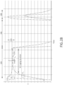
- FIG. 2B is a plot of voltage at various nodes of the bandwidth extension circuit 202 in FIG. 2A in response to an input signal, in accordance with one or more embodiments of the present disclosure.
- FIG. 2B illustrates voltages V d and V g during various transitions.
- FIG. 2B illustrates a pattern of bits (i.e., bit pattern) in which V d is high for several repeating bits (range 204), low for several repeating bits (range 206), and then high for a single bit (range 208).
- bit pattern i.e., bit pattern
- V d a difference between a peak voltage value 212 and an equilibrium voltage value 2114
- V d and V g are driven high (e.g., in the case of repeating bits).
- the feedback loop of the active inductor 110 generates a weaker, inverted, and delayed version of the data at the output of the driver 102 that is connected back to the output node of the driver 102 ( V d ). This is illustrated in FIG. 2B as a temporal delay between V g and V d during both low-to-high and high-to-low transitions. The values of V g and V d then reach an equilibrium after a settling time that may be reached in cases of repeating bits.
- HCI may typically occur when a transistor experiences large current flow associated with simultaneously driving the drain voltage and the gate voltage high for an NMOS device (or low for a PMOS device). Under these HCI aging conditions, charges may become trapped in a gate of the transistor resulting in reduced carrier mobility and reduced current capacity.
- BTI may typically be induced when the gate voltage is driven high for an NMOS device (or low for a PMOS device) for an extended time, particularly at relatively high temperatures, and results in trapped charges and increased operational voltage thresholds.
- the structural impact of BTI diminishes once BTI aging conditions are no longer present. In contrast, the structural impact of HCI typically does not diminish and slowly builds up upon increased exposure to HCI aging conditions.
- bandwidth extension circuit 202 illustrated in FIG. 2A is susceptible to both HCI and BTI aging conditions.
- simultaneously driving V g and V d high for extended durations corresponds to HCI aging conditions in the inverter 106 that reduce an operational lifetime of the bandwidth extension circuit 202.
- simultaneously driving both V g and V d high corresponds to high gate and drain voltages for the transistors M pa and M na of the inverter 106. Exposure to these conditions induces HCI that increases the threshold voltages of these transistors as well as reduces the current flow.
- these HCI aging conditions are the most pronounced in the range 204 where V d is driven high for repeating bits (e.g., relatively low frequency data patterns [e.g., bit pattern]).
- the values and/or sizes of various components in the bandwidth extension circuit 202 may influence both the duration of HCI aging conditions and the inductive peaking performance.
- relatively larger values of the resistor 104 and/or relatively larger values of a size ratio of the inverter 106 to the driver 102 provide relatively higher inductive peaking as well as slower aging.
- the inverter 106 is smaller than the driver 102 to provide feedback without overwhelming the driver 102.
- the amount of peaking required is predetermined by the communication channel conditions and may not be tweaked to improve other circuit aspects such as aging.
- the size of the inverter 106 increases the inductive peaking voltage 210 and also decreases the duration of the HCI aging conditions and the predicted aging impact.
- the size of the inverter 106 cannot be increased without limitation to fully mitigate aging.
- the size ratio of the inverter 106 to the driver 102 may be selected to provide a desired amount of inductive peaking (e.g., a desired inductive peaking voltage 210) for a desired bandwidth improvement without degrading performance in other ways.
- inductive peaking results in a reduction of the equilibrium voltage value 214 relative to the peak voltage value 212 in cases of a high V d value for repeating bits (e.g., the range 204, but relatively little change when V d is driven high for a single bit (e.g., the range 208). Accordingly, too much inductive peaking may result in substantially lower V d levels for repeating high bits relative to single high bits, which may negatively impact noise and/or transmission performance metrics.
- the presence of HCI aging conditions is a direct consequence of the use of an active inductor 110 design to provide inductive peaking. Further, aging may be most severe when no data is being input the bandwidth extension circuit 202 (e.g., a constant V in ) such that V d and V g are constant for extended periods of time, particularly if V d and V g are held at high levels for extended periods of time.
- V in bandwidth extension circuit 202
- the bandwidth extension circuit 202 illustrated in FIG. 2A is further susceptible to BTI aging conditions in some scenarios.
- the transistors within the driver 102 and/or the inverter 106 may be exposed to BTI aging conditions whenever V in is held constant since the gate voltage of either the driver 102 or the inverter 106 will be high regardless of the particular value of V in . Since BTI aging is largely reversable, BTI aging in the bandwidth extension circuit 202 in FIG. 2A may be mitigated by frequently toggling the input signal V in .
- bandwidth extension circuit 202 is not conducive to simultaneous mitigation of both HCI and BTI.
- a bandwidth extension circuit (e.g., the bandwidth extension circuit 202, the bandwidth extension circuit 100, a driver circuit, or the like) may generally be operated in at least two conditions, referred to herein as a run-time condition and a down-time condition.
- a signal applied to an input node ( V in ) may typically be modulated with data (e.g., a pattern of high and low bits, or other bit pattern) and a signal provided by the bandwidth extension circuit at an output node ( V out ) may be provided to and utilized by an external device or system.
- the bandwidth extension circuit may be connected to power, but a signal applied to the input node ( V in ) may typically not include meaningful data and the signal provided by the bandwidth extension circuit at an output node ( V out ) may typically not be utilized by an external device or a system.
- the signal applied to the input node ( V in ) may generally have any value including, but not limited to, a fixed value or a floating value.
- the down-time condition may occur between data streams or when a device is in a stand-by mode.
- BTI aging may generally be mitigated by frequent toggling of the input signal V in , which may naturally occur during run-time (or a run-time condition) when V in includes a signal modulated with data for transmission. Further, the input signal V in may be intentionally toggled when V in does not include a signal modulated with data for transmission, which is referred to herein as down-time or a down-time condition.
- the bandwidth extension circuit 202 suffers from HCI aging whenever V d and V g are simultaneously high for NMOS devices or simultaneously low for PMOS devices. As illustrated in FIG.
- V d may occur at least briefly when V d is driven high or low for a single bit (e.g., range 208) or when V d is driven high or low for multiple repeating bits (e.g., range 204 and range 206).
- toggling the input signal V in during down-time when V in does not include a signal modulated with data (or at least meaningful data) for transmission may mitigate BTI but not HCI.
- forcing V in at a low or high value during down-time while forcing V g to the same value and disconnecting the feedback resistor 104 through external power down switches may mitigate HCI in the inverter 106 but the driver 102 may be subjected to BTI.
- a bandwidth extension circuit 100 as disclosed herein including the switch 106 may enable operation of the bandwidth extension circuit 100 in a manner that mitigates aging of the constituent components (e.g., the inverter 106).
- the circuits, systems, and methods disclosed herein enable control over the frequency and/or duration that transistors within the bandwidth extension circuit 100 are operated under aging conditions such as, but not limited to, HCI or BTI aging conditions.
- the operational lifetime of the bandwidth extension circuit 100 as disclosed herein may be substantially longer than an operational lifetime of alternative bandwidth extension circuits such as, but not limited to, the design illustrated in FIG. 2A .
- the switch 106 in the bandwidth extension circuit 100 illustrated in FIGS. 1A and 1B enables operation of the bandwidth extension circuit 100 in two modes: the active mode in which the switch 106 is in a closed state (see e.g., the left panel 112 in FIG. 1B ) and a power-down mode in which the switch 106 is in an open state (see e.g., the right panel 114 in FIG. 1B ). HCI and/or BTI may be mitigated in each of these modes.
- the power-down mode may be suitable for, but is not limited to, operation during down-time when the input signal V in does not include modulated data.
- the switch 106 in an open state disrupts the feedback across the inverter 106.
- the output of the inverter 106 is connected to a first node ( n a ) of the switch 106 and V d (also V out ) is connected to a second node ( n b ) of the switch 106.
- the driver 102 and the inverter 106 are simply two cascaded inverters such that V d and V g are never simultaneously high or low, which mitigates HCI aging for both NMOS and PMOS device types.
- V d and V g are never simultaneously high or low, which mitigates HCI aging for both NMOS and PMOS device types.
- the disruption of the feedback in this power-down mode does not provide inductive peaking, inductive peaking is not needed when the input signal V in does not include modulated data.
- BTI may be mitigated by modulating the input signal V in artificially in the power-down mode. As a result, both HCI and BTI are mitigated in this power-down mode.
- the input signal ( V in ) may be modulated using any suitable pattern (e.g., bit pattern) including, but not limited to, alternating high and low bits, a random series of high and low bits, a pseudo-random series of high and low bits, or a preselected series of high and low bits.
- bit pattern e.g., bit pattern
- the active mode may be suitable for, but is not limited to, operation during run-time when the input signal V in is modulated with data.
- the inherent modulation of the input signal ( V in ) with data may largely mitigate BTI.
- a voltage drop across the switch 106 in series with the transistors M na and M pa of the inverter 106 e.g., between n a and V d ) may reduce the drain voltage of the transistor M na when V d is driven high (or the drain of the transistor M pa when V d is driven low) and thus decrease the severity and/or duration of HCI aging conditions for this transistor.
- HCI may be partially mitigated relative to alternative designs such as, but not limited to, the design illustrated in FIG. 2A even during run-time conditions.
- this voltage drop across the switch 106 e.g., associated with a resistance of the switch 106
- this switch may be implemented organically as a segment of the feedback resistor 104 by utilizing finger partitioning in case of a transistor implementation of this resistor.
- both the active and power-down operational modes may thus provide aging-averse operation of the bandwidth extension circuit 100 to prolong the operational lifetime of the bandwidth extension circuit 100.
- FIGS. 3A-4B simulated aging performance of the bandwidth extension circuit 100 in FIG. 1B is compared to the bandwidth extension circuit 202 in FIG. 2A .
- the conventional bandwidth extension circuit 202 in FIG. 2A exhibits the most severe aging in the down-time condition, whereas the aging averse bandwidth extension circuit 100 in FIG. 1B exhibits no (or negligible) detectable aging effects in this same condition. Further, although the aging averse bandwidth extension circuit 100 in FIG. 1B exhibits some detectable aging in the run-time mode, the effects are substantially reduced relative to the conventional bandwidth extension circuit 202 in FIG. 2A .
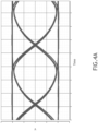
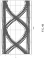
- FIGS. 3A-4B depict simulated eye diagrams before and after aging for the bandwidth extension circuit 100 in FIG. 1B and the bandwidth extension circuit 202 in FIG. 2A .
- FIG. 3A is an eye diagram for the bandwidth extension circuit 100 in FIG. 1B in a new state (e.g., prior to aging), in accordance with one or more embodiments of the present disclosure.
- FIG. 3B is an eye diagram for the bandwidth extension circuit 100 in FIG. 1B after aging for 10 years, in accordance with one or more embodiments of the present disclosure.
- FIG. 4A is an eye diagram for the bandwidth extension circuit 202 in FIG. 2A in a new state (e.g., prior to aging), in accordance with one or more embodiments of the present disclosure.
- FIG. 4B is an eye diagram for the bandwidth extension circuit 202 in FIG. 2A after aging for 10 years, in accordance with one or more embodiments of the present disclosure.
- the eye diagram of the aging averse bandwidth extension circuit 100 in FIG. 1B exhibits only minor changes after the simulated 10 years of aging, which indicates that the operational characteristics and associated noise metrics are relatively unchanged.
- the eye diagram of the conventional bandwidth extension circuit 202 in FIG. 2A exhibits substantial degradation after the simulated 10 years of aging.
- the eye diagram in FIG. 4B reveals a substantial decrease in the signal-to-noise ratio and a substantial increase in temporal variations.
- FIG. 5 is a block diagram of a system 502 including a bandwidth extension circuit 100, in accordance with one or more embodiments of the present disclosure. It is contemplated herein that a bandwidth extension circuit 100 may be implemented within any communications system including, but not limited to, a high-speed transceiver system (e.g., a wireline transceiver system).
- a bandwidth extension circuit 100 may be implemented within any communications system including, but not limited to, a high-speed transceiver system (e.g., a wireline transceiver system).
- a bandwidth extension circuit 100 may be implemented within systems such as, but not limited to, a SERDES system (e.g., a backplane SERDES system), a physical layer transceiver (PHY) (e.g., an ethernet PHY, or the like), an optical communications module (e.g., a pluggable optical communications module), or a coherent communications circuit.
- a SERDES system e.g., a backplane SERDES system
- PHY physical layer transceiver
- an optical communications module e.g., a pluggable optical communications module
- coherent communications circuit e.g., a coherent communications circuit.
- the system 502 may be generally suitable for a wide variety of applications and services such as, but not limited to, network switches, data center interconnects, coherent telecommunications solutions, high-speed PHY devices, or wireless base stations.
- a system 502 includes one or more bandwidth extension circuits 100 and a controller 504 to control the operational states of the bandwidth extension circuits 100.
- the controller 504 may be communicatively coupled with the bandwidth extension circuits 100 to control (e.g., via drive signals) whether the bandwidth extension circuits 100 are in the active mode or in the power-down mode.
- the controller 504 provides individual control of each of the bandwidth extension circuits 100. In this way, some bandwidth extension circuits 100 may be in an active mode while others may be in a power-down mode.
- the controller 504 controls all of the bandwidth extension circuits 100 together such that each of the bandwidth extension circuits 100 operate in the same mode.
- the bandwidth extension circuits 100 may be arranged in any suitable configuration. In some embodiments, two or more bandwidth extension circuits 100 are arranged along a transmission path to promote data integrity along the transmission path for a desired transmission distance. In some embodiments, two or more bandwidth extension circuits 100 are arranged along different transmission paths corresponding to different communication channels. In this way, the system 502 may provide or facilitate multi-channel communications. It is to be understood that these examples are illustrative only and are not limiting on the present disclosure.
- the controller 504 may be connected to the switches 106 of the bandwidth extension circuits 100. In this way, the controller 504 may direct a particular bandwidth extension circuit 100 to operate in the active mode (e.g., as depicted in the left panel 112 of FIG. 1B ) by directing the constituent switch 106 to be in the closed state and/or to operate in the power-down mode (e.g., as depicted in the right panel 114 of FIG. 1B ) by directing the constituent switch 106 to be in the closed state.
- the active mode e.g., as depicted in the left panel 112 of FIG. 1B
- the constituent switch 106 to be in the closed state
- the power-down mode e.g., as depicted in the right panel 114 of FIG. 1B
- the controller 504 may have any architecture suitable for selectively modifying the states of the bandwidth extension circuits 100 or the constituent switches 106.
- the controller 504 includes one or more processors configured to execute program instructions.
- the program instructions may be stored on a memory device such as, but not limited to, read-only memory (ROM), random-access memory (RAM), or a solid-state drive.
- the controller 504 may include any type of processing or logic circuitry such as, but not limited to, a microprocessor, an application specific integrated circuit (ASIC), a field programmable gate array (FPGA), or a digital signal processor (DSP).
- ASIC application specific integrated circuit
- FPGA field programmable gate array
- DSP digital signal processor
- the system 502 further includes a source 506 to provide one or more signals (e.g., input signals V in ) to the bandwidth extension circuits 100.
- the source 506 may provide the same signals to each bandwidth extension circuit 100 or different signals to different bandwidth extension circuits 100.
- one or more signals are received from an external system or device.
- a signal including modulated data may be received from any location including the source 506 or an external system.
- the controller 504 directs a bandwidth extension circuit 100 to operate in the active mode (e.g., as depicted in the left panel 112 of FIG. 1B ) when a signal directed to that bandwidth extension circuit 100 includes data.
- a signal directed to that bandwidth extension circuit 100 includes data.
- a run-time condition such a signal may include high and low bits (e.g., high and low voltage values) associated with data encoded using any technique known in the art. This signal may then be transmitted to an external device or system.
- the controller 504 directs a bandwidth extension circuit 100 to operate in the power-down mode (e.g., as depicted in the right panel 114 of FIG. 1B ) when a signal directed to that bandwidth extension circuit 100 does not include data.
- a bandwidth extension circuit 100 may be referred to as a down-time condition.
- power may be supplied to the bandwidth extension circuits 100 (e.g., through one or more power sources not explicitly illustrated), but the signal provided to the bandwidth extension circuit 100 may not have any meaningful data for transmission. Accordingly, operation in the power-down mode may mitigate HCI as described previously herein.
- the source 506 provides an arbitrary signal to the bandwidth extension circuit 100 in the power-down mode, where the arbitrary signal includes multiple transitions between high and low values to mitigate BTI in the bandwidth extension circuit 100 as described previously herein.
- This arbitrary signal may have any pattern of high and low bits (e.g., high and low voltages) including, but not limited to, an alternating pattern of high and low bits at any frequency and/or duty cycle, a random series of high and low bits, a pseudo-random series of high and low bits, or a pre-defined series of high and low bits.
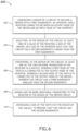
- FIG. 6 is a flow diagram illustrating steps performed in a method 600 for designing a circuit (e.g., a bandwidth extension circuit), in accordance with one or more embodiments of the present disclosure. Applicant notes that the embodiments and enabling technologies described previously herein in the context of the bandwidth extension circuit 100 should be interpreted to extend to the method 600. It is further noted, however, that the method 600 is not limited to the architecture of the bandwidth extension circuit 100.
- a circuit e.g., a bandwidth extension circuit
- the method 600 is not limited to the particular steps depicted in FIG. 6 .
- the method 600 includes additional steps, which may be performed before the depicted steps, after the depicted steps, and/or between any of the depicted steps. In some embodiments, not all of the steps depicted in FIG. 6 are performed.
- the method 600 includes a step 602 of generating a design of a circuit (e.g., a bandwidth extension circuit, a driver circuit, a device, or the like) to include a driver 102 with a first bandwidth, an inverter 106, and a resistor 104 connected between an output node of the driver 102 and an input node of the inverter 106.
- a circuit e.g., a bandwidth extension circuit, a driver circuit, a device, or the like
- a driver 102 with a first bandwidth
- an inverter 106 e.g., a driver 106
- a resistor 104 connected between an output node of the driver 102 and an input node of the inverter 106.
- an input node of the driver 102 may correspond to an input node of the circuit
- the output node of the driver may correspond to an output node of the circuit.
- Bandwidth may be the maximum rate of transfer for an electronic signal (e.g., data or current).
- the resistor 104 may have any design suitable with a selected fabrication process.
- the resistor 104 includes two or more transistors (e.g., MOSFET transistors or any other suitable transistors) with a common gate electrode.
- the resistor 104 may include a multi-finger gate electrode distributed over one or more doped semiconductor regions.
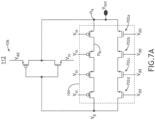
- FIG. 7A is a simplified schematic of an active inductor 110 formed as an inverter 106 and a resistor 104 as depicted in the bandwidth extension circuit 202 of FIG. 2A , in accordance with one or more embodiments of the present disclosure.
- FIG. 7A illustrates a configuration of the resistor 104 with four transistor pairs 702a-d, each formed as MOSFET transistors arranged to provide current flow with a specified resistance (e.g., the level of opposition to the flow of an electrical current).
- the four transistor pairs 702a-d may be formed with a common gate electrode having multiple series fingers (e.g., as a multi-finger device).
- the method 600 includes a step 604 of selecting, in the design of the circuit, at least one of a value of the resistor 104, a size of the driver 102, or a size of the inverter 106 such that the circuit has a second bandwidth larger than the first bandwidth.
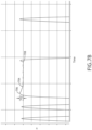
- FIG. 7B is a graph including a plot 704 of voltage at an output node of a bandwidth extension circuit for a series of bits, in accordance with one or more embodiments of the present disclosure.
- FIG. 7B corresponds to a high bit, a low bit, a high bit, a low bit, a repeating series of high bits, a repeating series of low bits, and a high bit.
- Inductive peaking is evident in the plot of FIG. 7B , particularly in the series of repeating high bits.
- the transition to the series of high bits exhibits a peak voltage value 706 that decays to an equilibrium voltage value 708.
- inductive peaking may be characterized in step 602 by any suitable metric such as, but not limited to, an inductive peaking voltage 710 associated with a difference between the peak voltage value 706 and the equilibrium voltage value 708.
- the method 600 includes a step 606 of converting, in the design of the circuit, at least one of the two or more transistors in the resistor 104 to a switch 106, where a first node of the switch 106 is connected to the output node of the inverter 106, where a second node of the switch 106 is connected to the output node of the driver 102, and where the circuit has a third bandwidth smaller than the second bandwidth.
- converting at least one of the two or more transistors in the resistor 104 into a switch 106 may be carried out by separating the gate electrodes of the transistors forming the switch 106 from the other transistors forming the resistor 104 and moving an output node ( V out ) of the active inductor 110 from node n a to node n b providing a connection to the output node of the driver 102 (e.g., V d in FIG. 1B ).
- the step 606 may be carried out by moving the output node ( V out ) providing the connection to the output node of the driver 102 ( V d ) by one finger to the left.
- FIG. 8A is a simplified schematic of the active inductor 110 in FIG. 7A in which one transistor pair 702a of the resistor 104 is converted to a switch 106, in accordance with one or more embodiments of the present disclosure.
- FIG. 8A illustrates conversion of transistor pair 702a to a switch 106 by moving the output node ( V out ) by one finger to the left for connection to the output of the driver 102 ( V d ) as well modifying the gate nodes 802 (depicted as pd and pd b ) to provide control of a state of the switch 106 (e.g., via the controller 504 as depicted in FIG. 5 ).
- the switch 106 may operate an open state or a closed state based on control signals provided to the gate nodes 802.
- FIG. 8B is a graph including FIG. 7B plus an additional plot 804 illustrating a voltage at the output node (e.g., V out in FIG. 1B ) of the bandwidth extension circuit based on the design of the active inductor 110 in FIG. 8A , in accordance with one or more embodiments of the present disclosure. As illustrated in FIG. 8B , converting at least one of the transistors of the resistor 104 to a switch 106 may decrease the inductive peaking voltage 210.
- the method 600 includes a step 608 of adding one or more additional transistors to the resistor 104 in the design of the circuit.
- one or more additional transistors may be added between the output node ( V out ) for connection to the output of the driver 102 ( V d ) and the input node of the inverter 106 ( V g ). This may provide recovery of some of the lost peaking from step 606.
- the step 606 may be carried out by adding one or more additional fingers in series to the resistor 104 between nodes n b and V g .
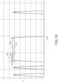
- FIG. 9 is a graph including FIG. 8B plus an additional plot 902 illustrating a voltage at the output node (e.g., V out in FIG. 1B ) of a bandwidth extension circuit based on the design of the active inductor 110 in FIG. 9 , in accordance with one or more embodiments of the present disclosure. As illustrated in FIG. 9 , a portion of the inductive peaking voltage 710 is recovered by the addition of the transistor pair 702e.
- the method 600 includes a step 610 of increasing a size of the switch 106 in the design of the circuit to provide that the circuit has the second bandwidth.
- the size of the switch 106 may be increased by any amount suitable for recovering additional inductive peaking.
- the step 610 includes doubling a size of the switch 106.
- the step 610 includes increasing a number of fins of one or more transistors in the switch 106.
- the switch 106 may include one or more finFET transistors in which doped semiconductor regions are formed as one or more fins that are at least partially surrounded by a gate electrode.
- a finFET transistor width is dependent on its number of fins and is typically expressed in an n X m format where n represents the number of fingers and m represents the number of fins per finger.
- the step 610 may include converting the transistor pair 702a associated with the switch 106 to a 2x3 fin device.
- the inverter 106 may be of any suitable size including, but not limited to, a 2x3 fin device.
- FIG. 10 is a graph including FIG.
- the inductive peaking (e.g., as measured by the inductive peaking voltage 710) is restored.
- the designed circuit e.g., the bandwidth extension circuit 100 illustrated in FIG. 1B
- the switch 106 may have the same or substantially the same inductive peaking performance as a traditional bandwidth extension circuit 202 without the switch 106 while providing an aging-averse operation and a correspondingly longer operational lifetime without incurring any considerable bandwidth penalty.
- the method 600 includes a step of fabricating the circuit based on the design of the circuit.
- the circuit and the constituent components may be fabricated using any technology or fabrication processes known in the art.
- constituent transistors may include, but are not limited to CMOS transistors, FET transistors, or BJT transistors.
- FIGS. 7B , 8B , 9 , and 10 directly illustrate bandwidth values.
- the figures instead illustrate inductive peaking, which may impact bandwidth and be used as a bandwidth extension technique.
- any two components herein combined to achieve a particular functionality can be seen as “associated with” each other such that the desired functionality is achieved, irrespective of architectures or intermedial components.
- any two components so associated can also be viewed as being “connected” or “coupled” to each other to achieve the desired functionality, and any two components capable of being so associated can also be viewed as being “couplable” to each other to achieve the desired functionality.
- Specific examples of couplable include but are not limited to physically interactable and/or physically interacting components and/or wirelessly interactable and/or wirelessly interacting components and/or logically interactable and/or logically interacting components.
Landscapes
- Engineering & Computer Science (AREA)
- Power Engineering (AREA)
- Theoretical Computer Science (AREA)
- Physics & Mathematics (AREA)
- Computer Hardware Design (AREA)
- Computing Systems (AREA)
- General Engineering & Computer Science (AREA)
- Mathematical Physics (AREA)
- Electronic Switches (AREA)
- Logic Circuits (AREA)
Abstract
Description
- The present disclosure is directed to an apparatus for performing bandwidth extension and, more particularly, to an apparatus providing bandwidth extension in a manner that mitigates aging issues.
- To meet stringent data-rate requirements of high-end serializer/deserializer (SERDES) products, advanced complementary metal-oxide-semiconductor (CMOS) technology processes and on-chip bandwidth extension techniques are commonly considered to achieve reasonable intersymbol interference (ISI) and reliable bit error rates (BER).
- Inductive peaking is one approach that may be employed to boost high-frequency gain to compensate for bandwidth limitations (i.e., a limit within a band of wavelengths, frequencies, or energies). In particular, an active inductor implementation using only transistors may be desirable since an active inductor may occupy a relatively smaller area than a passive inductor and may further be compatible with switching CMOS circuits.
- However, active inductors typically suffer from destructive aging effects that may result in degraded performance over time and ultimately limit an operational lifetime. The aging problems are often exacerbated by adverse operating conditions for high-speed SERDES circuits such as high-temperature operation and power supplied by voltages that are higher than typical foundry recommendations.
- There is therefore a need to develop systems and methods to cure the above deficiencies.
- A circuit is disclosed in accordance with one or more illustrative embodiments of the present disclosure. In one illustrative embodiment, the circuit includes a driver and an inverter. In another illustrative embodiment, the circuit includes a resistor between an output node of the driver and an input node of the inverter, where a first node of the resistor is connected to the output node of the driver and a second node of the resistor is connected to the input node of the inverter. In another illustrative embodiment, the circuit includes a switch between an output node of the inverter and the first node of the resistor, where an input node of the driver corresponds to an input node of the circuit, and where the output node of the driver corresponds to an output node of the circuit.
- A system is disclosed in accordance with one or more illustrative embodiments of the present disclosure. In one illustrative embodiment, the system includes one or more circuits, each comprising a driver, an inverter, a resistor connected between an output node of the driver and an input node of the inverter, and a switch between an output node of the inverter and the first node of the resistor. The first node of the resistor may be connected to the output node of the driver and a second node of the resistor may be connected to the input node of the inverter. An input node of the driver may correspond to an input node of the circuit and the output node of the driver may correspond to an output node of the circuit. In another illustrative embodiment, the system includes a controller coupled to the one or more circuits, where the controller independently directs the switch in each of the one or more circuits to operate in one of an open state or a closed state.
- A method is disclosed in accordance with one or more illustrative embodiments of the present disclosure. In one illustrative embodiment, the method includes generating a design of a circuit including a driver with a first bandwidth, an inverter, and a resistor connected between an output node of the driver and an input node of the inverter. In another illustrative embodiment, the resistor is formed from two or more transistors. A first node of the resistor may be connected to the output node of the driver and a second node of the resistor may be connected to the input node of the inverter. In another illustrative embodiment, an output node of the inverter is connected to the output node of the driver. An input node of the driver may correspond to an input node of the circuit, wherein the output node of the driver corresponds to an output node of the circuit. In another illustrative embodiment, the method includes selecting, in the design of the circuit, at least one of a value of the resistor, a size of the driver, or a size of the inverter such that the circuit has a second bandwidth larger than the first bandwidth. In another illustrative embodiment, the method includes converting, in the design of the circuit, at least one of the two or more transistors in the resistor to a switch, where a first node of the switch is connected to the output node of the inverter, where a second node of the switch is connected to the output node of the driver, and where the circuit has a third bandwidth smaller than the second bandwidth. In another illustrative embodiment, the method includes adding one or more additional transistors to the resistor in the design of the circuit. In another illustrative embodiment, the method includes increasing a size of the switch in the design of the circuit to provide that the circuit has the second bandwidth.
- It is to be understood that both the foregoing general description and the following detailed description are exemplary and explanatory only and are not necessarily restrictive of the invention as claimed. The accompanying drawings, which are incorporated in and constitute a part of the specification, illustrate embodiments of the invention and together with the general description, explain the principles of the invention.
- The numerous advantages of the disclosure may be better understood by those skilled in the art by reference to the accompanying figures.
-
FIG. 1A is a schematic view of a bandwidth extension circuit, in accordance with one or more embodiments of the present disclosure. -
FIG. 1B illustrates the bandwidth extension circuit including complementary metal-oxide-semiconductor (CMOS) components, in accordance with one or more embodiments of the present disclosure. -
FIG. 2A is a schematic view of a CMOS bandwidth extension circuit including an active inductor and without the switch illustrated inFIGS. 1A and1B , in accordance with one or more embodiments of the present disclosure. -
FIG. 2B is a plot of voltage at various nodes of the bandwidth extension circuit inFIG. 2A in response to an input signal, in accordance with one or more embodiments of the present disclosure. -
FIG. 3A is an eye diagram for the bandwidth extension circuit inFIG. 1B in a new state (e.g., prior to aging), in accordance with one or more embodiments of the present disclosure. -
FIG. 3B is an eye diagram for the bandwidth extension circuit inFIG. 1B after aging for 10 years, in accordance with one or more embodiments of the present disclosure. -
FIG. 4A is an eye diagram for the bandwidth extension circuit inFIG. 2A in a new state (e.g., prior to aging), in accordance with one or more embodiments of the present disclosure. -
FIG. 4B is an eye diagram for the bandwidth extension circuit inFIG. 2A after aging for 10 years, in accordance with one or more embodiments of the present disclosure. -
FIG. 5 is a block diagram of a system including abandwidth extension circuit 100, in accordance with one or more embodiments of the present disclosure. -
FIG. 6 is a flow diagram illustrating steps performed in a method for designing a bandwidth extension circuit, in accordance with one or more embodiments of the present disclosure. -
FIG. 7A is a simplified schematic of an active inductor formed as an inverter and a resistor as depicted in thebandwidth extension circuit 202 ofFIG. 2A , in accordance with one or more embodiments of the present disclosure. -
FIG. 7B is a graph including a plot of voltage at an output node of a bandwidth extension circuit for a series of bits, in accordance with one or more embodiments of the present disclosure. -
FIG. 8A is a simplified schematic of the active inductor inFIG. 7A in which one transistor pair of the resistor is converted to a switch, in accordance with one or more embodiments of the present disclosure. -
FIG. 8B is a graph includingFIG. 7B plus an additional plot of a voltage at the output node of the bandwidth extension circuit based on the design of the active inductor inFIG. 8A , in accordance with one or more embodiments of the present disclosure. -
FIG. 9 is a graph includingFIG. 8B plus an additional plot of a voltage at the output node of a bandwidth extension circuit based on the design of the active inductor inFIG. 8A , in accordance with one or more embodiments of the present disclosure. -
FIG. 10 is a graph includingFIG. 9 plus an additional plot of a voltage at the output node of a bandwidth extension circuit based on the design of the active inductor inFIG. 8A after increasing a size of the switch, in accordance with one or more embodiments of the present disclosure. - Reference will now be made in detail to the subject matter disclosed, which is illustrated in the accompanying drawings. The present disclosure has been shown and described with respect to certain embodiments and specific features thereof. The embodiments set forth herein are taken to be illustrative rather than limiting. It should be readily apparent to those of ordinary skill in the art that various changes and modifications in form and detail may be made without departing from the spirit and scope of the disclosure.
- As used herein, directional terms such as "top," "bottom," "over," "under," "upper," "upward," "lower," "down," and "downward" are intended to provide relative positions for purposes of description and are not intended to designate an absolute frame of reference. Various modifications to the described embodiments will be apparent to those with skill in the art, and the general principles defined herein may be applied to other embodiments.
- It is to be understood that depicted architectures are merely exemplary and that many other architectures can be implemented which achieve the same functionality. In a conceptual sense, any arrangement of components to achieve the same functionality is effectively "associated" such that the desired functionality is achieved. Hence, any two components herein combined to achieve a particular functionality can be seen as "associated with" each other such that the desired functionality is achieved, irrespective of architectures or intermedial components. Likewise, any two components so associated can also be viewed as being "connected," or "coupled," to each other to achieve the desired functionality, and any two components capable of being so associated can also be viewed as being "couplable," to each other to achieve the desired functionality. Additionally, it is envisioned, a coupling may include intervening elements or members between coupled members which are electrically or communicatively coupled.
- Unless otherwise indicated, a description indicating that one component is "connected to" another component (alternatively "located on," "disposed on," or the like) or "between" two components indicates that such components are functionally connected and does not necessarily indicate that such components are physically in contact. Rather, such components may be in physical contact or may alternatively include intervening elements. The term node (or alternatively, terminal) is used herein to indicate a point of connection between circuit elements or portions thereof. In this way, Components connected to a node may be physically connected in any suitable manner. In some embodiments, components connected to a node share a common electrical contact and may thus be, but are not required to be, physically proximate. In some embodiments, components connected to a node are connected through one or more electrically-conductive pathways such as, but not limited to, traces or wires. Further, components may be described as having one or more nodes (e.g., an input node, an output node, or the like) to indicate points for connection to other components. It is contemplated herein that descriptions of the connections between circuit components using nodes is solely for illustrative purposes and does not imply any particular technique for connecting such components.
- Embodiments of the present disclosure are directed to systems and methods for providing bandwidth extension of a driver in a manner that mitigates adverse effects of aging to promote relatively long operational lifetimes. A driver may include any type of device that repeats and/or amplifies a signal (e.g., a logic signal) such as, but not limited to, an inverter (e.g., a device that converts a logical high to a logical low or vice versa) or a buffer (e.g., a device that provides a logical high output in response to a logical high input and provides a logical low output in response to a logical low input). Some embodiments of the present disclosure are directed to bandwidth extension utilizing an active inductor providing inductive peaking. For example, a driver (e.g., an inductor, a buffer, or the like) may provide a baseline bandwidth (e.g., a first bandwidth). However, this first bandwidth may be extended (e.g., to a second bandwidth) by an inverter or a bandwidth extension circuit more generally. For example, a bandwidth extension circuit may include a driver, where an output node of a driver is connected to the input node of an inverter through a resistor, and where the active inductor further includes a switch between an output node of the inverter and the output node of the driver. A resistor may be any component that limits or regulates the flow of electric current in a circuit. Such a circuit may be operated either with the switch in a closed position to provide inductive peaking based on feedback from the inverter or with the switch in an open position without feedback.
- A bandwidth extension circuit and associated components (e.g., constituent inverters, or the like) may operate as logic devices designed to input and output a high bit (e.g., a logical "1") or a low bit (e.g., a logical "0"). The actual voltage values associated with a high bit (e.g., a high voltage value) or a low bit (e.g., a low voltage value) may depend on the fabrication process and/or the specific design. In some embodiments, a high voltage value associated with a high bit corresponds to an ideal value of 1 V, while a low voltage value associated with a low bit corresponds to an ideal value of 0V. Such a configuration may be suitable for a variety of fabrication processes including, but not limited to, complementary metal-oxide-semiconductor (CMOS) processes or transistor-transistor logic (TTL) processors. However, other embodiments may allow different high voltage values for high bits such as, but not limited to, 5V, 10 V, or 18 V. Further, it is to be understood that logic devices may generally operate with input and output voltages within operational ranges for both high bits and low bits. For the purposes of the present disclosure, the terms high voltage, high voltage value, and high bit are used interchangeably to refer to a logical high state and may include an associated operational voltage range. Similarly, the terms low voltage, low voltage value, and low bit are used interchangeably to refer to a logical low state and may include an associated operational voltage range.
- An inverter (e.g., a driver and/or the inverter coupled with a driver for bandwidth extension) may include any device that provides a logical inverse operation. For example, an inverter may output a low bit upon receiving a high bit and may output a high bit upon receiving a low bit. Further, such an inverter may be fabricated using any suitable processes or technology. In this way, an inverter of a bandwidth extension circuit as disclosed herein may include, but is not limited to, one or more field-effect transistors (FETs), one or more finFETs, one or more MOSFETs, one or more bipolar junction transistors (BJTs), one or more junction field-effect transistors (JFETs), one or more insulated-gated bipolar transistors (IGBTs), one or more high-electron-mobility transistors (HEMTs), one or more tunnel field-effect transistors (TFETs), one or more carbon nanotube FETs (CNTFETs), or one or more junction-less nanowire transistors (JLNTs). As a non-limiting illustration, an inverter fabricated according to CMOS processes (e.g., a CMOS inverter) may include two complementary transistors (e.g., a PMOS transistor and an NMOS transistor) with a common gate electrode, where a drain of the PMOS transistor is connected to a drain of the NMOS transistor. A transistor may be any device that regulates, controls, amplifies, or switches an electrical signal.
- An active inductor may include one or more transistors and potentially other components arranged to provide an inductance. An active inductor may be contrasted with a passive inductor, which is typically formed from a wire wrapped around a coil to store energy in a magnetic field. Active inductors may typically be fabricated with a smaller size than passive inductors, may provide additional flexibility and/or tunability relative to a passive inductor, and may be compatible with common fabrication processes such as, but not limited to, CMOS fabrication processes. As used herein, a size of a component may refer to the physical size of the component (e.g., width). In this way, an active inductor may be fabricated as an on-chip device in tight form factors using CMOS-compatible manufacturing techniques.
- Additionally, a switch as used herein may include one or more transistors arranged to operate in a closed state or an open state with respect to an input node and an output node, where an operational state of the switch may be controlled by a drive signal. For example, a switch operating in an open state (e.g., a non-conducting state) may restrict or eliminate current flow between the input node and the output node, whereas a switch operating in a closed state (e.g., a conducting state) may allow current flow between the input node and the output node.
- It is recognized herein that operating a transistor under certain conditions (referred to herein as aging conditions) may induce structural changes that may degrade performance but not result in abrupt device breakdown, a phenomenon referred to herein as aging. A transistor may be operated under such aging conditions for extended periods of time without catastrophic breakdown. However, extended operation under aging conditions may typically result in a reduced operational lifetime of that transistor compared to operation under less damaging conditions.
- As an illustration, two significant sources of aging transistors include hot carrier injection (HCI) and bias temperature instability (BTI). HCI may typically occur when a transistor simultaneously experiences high drain-source (Vds ) and gate-source (Vgs ) voltages, which may be associated with large current flow. When such conditions are present, charges may become trapped in a gate of the transistor resulting in reduced carrier mobility and reduced current capacity. In many cases, the effects of HCI aging are not reversable. BTI may be typically induced under conditions of high gate voltage and/or high temperature and results in trapped charges and reduced operational voltage thresholds. In many cases, long-term effects of BTI may be partially reversed by periodically inverting the gate voltage polarity. For this reason, one approach to mitigating BTI is to modulate the gate voltage (e.g., alternate between high bits and low bits) when possible. It is to be understood that the description of aging conditions in MOS devices is provided solely for illustrative purposes and are not limiting on the circuits, systems and method disclosed herein. It is contemplated that a bandwidth extension circuit as disclosed herein may be operational in a manner that mitigates aging regardless of the selected fabrication process. In this way, the circuits, systems and methods disclosed herein are not limited to devices using CMOS inverters, but may extend to alternative technologies including, but not limited to, FET inverters more generally, BJT inverters, or other inverter types including a switch.
- Many active inductor designs include transistors that are exposed to aging conditions for extended times under normal operation and thus typically suffer from relatively low operational lifetimes. Further, typical approaches for mitigating aging in active inductors prioritize mitigation of one source of aging (e.g., HCI or BTI) over another depending on a mode of operation of the circuit.
- However, a bandwidth extension circuit including an active inductor as disclosed herein may substantially limit exposure of constituent transistors to aging conditions and may thus have substantially longer lifetimes than alternative designs. In this way, such a circuit (or components thereof including the active inductor) may be aging averse.
- A bandwidth extension circuit as disclosed herein may be operable in different modes depending on a state of the switch to provide aging-averse operation.
- For example, operation of the bandwidth extension circuit with the switch in a closed mode is referred to herein as an active mode. In this active mode, the closed switch may connect the output nodes of the two inverters, which also induces feedback across the inverter such that the device operates as an active inductor. Further, the circuit in the active mode may provide inductive peaking and may thus be used to compensate for bandwidth limitations of a communications system such as, but not limited to, a serializer/deserializer (SERDES) system.
- It is contemplated herein that signals provided to the bandwidth extension circuit during the active mode (e.g., signals including data to be transmitted) typically include many transitions between high and low voltages (e.g., the signal includes transitions between high and low bits) such that BTI effects are negligible or at least within acceptable tolerances.
- However, operation in the active mode may expose at least some transistors within the inverters to conditions that produce HCI. For example, operation with a high input voltage (e.g., a high bit in an input signal) may result in relatively large drain-source (Vds ) and/or gate-source (Vgs ) voltages and associated relatively high current flow due to feedback from the inverter. Since this feedback condition is necessary for the operation of the device to provide inductive peaking, HCI under these conditions may be unavoidable to some extent. However, it is further contemplated herein that the presence of the switch may reduce the required drain-source (Vds ) across the transistors constituting the inverter relative to a design without the switch such that aging may be substantially reduced relative to a design without the switch.
- As another example, operation of the bandwidth extension circuit with the switch in an open mode is referred to herein as a power-down mode.
- It is contemplated herein that typical bandwidth extension circuit designs operate under particularly damaging aging conditions when an input signal is constant (e.g., either as a high bit or a low bit) for an extended time. In the context of a communications system, this may occur when no information is being communicated. Under these conditions, conditions for both HCI and BTI may be present. Modulation of the input signal in these conditions (e.g., providing an arbitrary input signal with randomized data) may mitigate BTI but not HCI. This may be particularly the case when the frequency of the alternating input data pattern is slow (e.g., when data is not actively being provided to the circuit). To avoid HCI in this mode of operation, the driver gate voltage and the inverter gate voltage can be tied to opposite polarities through additional power-down switches while disconnecting the feedback resistor. However, in this case, the input data cannot be continuously toggled to mitigate BTI aging as may be the case when no additional power down switches are used. That is to say, there exists some conflict between the mitigation of BTI and HCI simultaneously for an active peaked circuit.
- However, operation of a bandwidth extension circuit as disclosed herein in the power-down mode may mitigate both BTI and HCI. In this power-down mode, the output nodes of the two inverters are decoupled such that the two inverters are simply in series with the resistor between them, which eliminates fighting amongst them to pull the output node in opposite directions as may be the case if no switch is used. As a result, the feedback conditions that contribute to HCI are removed. Further, modulation of the input signal in this power-down mode may also mitigate BTI as there is no need to inversely correlate the gate voltages of the driver and the inverter continuously as would be the case if no such decoupling between the driver and inverter is implemented.
- Additional embodiments of the present disclosure are directed to a communications system including at least one bandwidth extension circuit with a switch as disclosed herein, as well as a controller for controlling the operational mode of the switch. In this way, the controller may selectively operate one or more bandwidth extension circuits in the active mode or the power-down mode. The communications system may further include a source to provide or otherwise control an input signal to one or more bandwidth extension circuits. In some embodiments, the controller is further coupled to the source and may direct the source to provide a modulated input signal (e.g., including randomized data, alternating high and low voltages, or the like) to one or more bandwidth extension circuits when in a power-down mode to mitigate aging of the active inductor during the power-down mode.
- Additional embodiments of the present disclosure are directed to methods for designing a bandwidth extension circuit as disclosed herein. For example, the method may include, but is not limited to, selecting initial values and/or sizes of various components of a bandwidth extension circuit with an active inductor to provide a desired amount of inductive peaking, adding a switch to selectively provide feedback based on the active inductor, determining a reduction of the inductive peaking performance due to the switch, and adjusting the values of at least some of the values and/or sizes of the components to at least partially compensate for the reduction of the performance due to the switch.
- As is known, one or more transistors (e.g., FET transistors) may be fabricated with varied designs of the physical layout between a gate structure and doped material forming drain and source regions. In particular, a gate structure (e.g., a gate electrode) may be fabricated as a single strip (e.g., a 1-finger design) or as multiple connected strips (e.g., a multi-finger design) over doped regions, where the term finger (e.g., a transistor pair) denotes a number of such strips. For example, a 1-finger design may include a gate structure with a single strip, a 2-finger design may include a gate structure with two strips, and so on. Multi-finger designs may be utilized for various reasons including, but not limited to, controlling a physical layout size or a gate resistance. Further, multi-finger layouts may be used to fabricate multiple connected devices as will be described in greater detail below.
- Referring now to
FIGS. 1A-10 , circuits, systems and methods for bandwidth extension (e.g., using inductive peaking, or the like) with an active inductor are described in greater detail, in accordance with one or more embodiments of the present disclosure. -
FIG. 1A is a schematic view of abandwidth extension circuit 100, in accordance with one or more embodiments of the present disclosure. In some embodiments, thebandwidth extension circuit 100 includes a first driver (referred to herein as a driver 102) in series with aresistor 104 and aninverter 106. Thedriver 102 may include any type of driver circuit known in the art such as, but not limited to, a buffer or an inverter (e.g., as illustrated inFIG. 1A ). Further, theinverter 106 may be, but is not limited to, an inverter. For example, theresistor 104 may be connected between an output node of thedriver 102 and an input node of theinverter 106. Thebandwidth extension circuit 100 may further include aswitch 106 between an output node of theinverter 106 and the output node of thedriver 102. In this configuration, an input node of the bandwidth extension circuit 100 (Vin ) may correspond to the input node of thedriver 102 and an output node of the bandwidth extension circuit 100 (Vout ) may correspond to the output node of thedriver 102.FIG. 1A further depicts aload capacitance 108, which may be associated with various internal capacitances of the components of the bandwidth extension circuit 100 (e.g., thedriver 102, theinverter 106, and/or any additional components) and/or an additional capacitor. - In a general sense, the
bandwidth extension circuit 100 may be characterized as a drive circuit and may be suitable as a repeater to strengthen a transmitted signal, which may be suitable for, but is not limited to, extending a transmission range of the signal. - The
bandwidth extension circuit 100 may be operable in different modes depending on a state of the switch 106 (e.g., whether theswitch 106 is in a closed state or an open state). - Operation of the
switch 106 in a closed state may enable feedback across theinverter 106. In this mode, referred to herein as an active mode, theresistor 104 and theinverter 106 may operate as anactive inductor 110 load to thedriver 102. Such abandwidth extension circuit 100 may be characterized as a shunt-peaked driver using theactive inductor 110. Thisactive inductor 110 may be suitable for providing inductive peaking to boost a high-frequency gain of thebandwidth extension circuit 100. For example, a typical driver circuit including only thedriver 102 may have a bandwidth that is limited by its drive resistance and load capacitance. However, this bandwidth may be increased using inductive peaking with a series peaking inductor (e.g., as illustrated inFIG. 1A with the active inductor 110) having a resonance frequency at or near a 3-dB bandwidth of thebandwidth extension circuit 100. In particular, inductive peaking is generated in thebandwidth extension circuit 100 by inducing theinverter 106 at a weaker, inverted, and delayed version of the signal at thedriver 102 output. For fast-changing data, theinverter 106 has insufficient time to react, and the gain of thedriver 102 may be large. Whereas, for slow changing data, theinverter 106 output contends with thedriver 102 output, reducing its gain. The use of an active inductor (e.g., theactive inductor 110 inFIG. 1A ) for inductive peaking instead of a passive inductor may provide a compact solution that is compatible with digital circuitry fabrication processes (e.g., CMOS processes or the like) and is suitable for use on multiple bit lines. - Operation of the
switch 106 in an open state may decouple the outputs of theinverter 106 and thedriver 102. In this mode, referred to herein as a power-down mode, thedriver 102 and theinverter 106 operate as two cascaded inverters with no feedback between the respective output nodes. As a result, thebandwidth extension circuit 100 does not provide active peaking in this power-down mode. However, it is contemplated herein that inductive peaking may not be necessary in this power down mode (e.g., when input signals applied to Vin do not contain meaningful data) and that disrupting the feedback between theinverter 106 and thedriver 102 may mitigate aging. - The
bandwidth extension circuit 100 may be fabricated using any type of components known in the art. In some embodiments, thebandwidth extension circuit 100 is fabricated using MOS components. For example, thedriver 102 and/or theactive inductor 110 may include CMOS transistors (e.g., pairs of complementary p-type and n-type MOSFETs). As another example, theswitch 106 and/or theresistor 104 may be fabricated as MOS elements. However, in a general sense, the components of thebandwidth extension circuit 100 may be fabricated using any transistor technology or fabrication process. For instance, components of thebandwidth extension circuit 100 may include, but are not limited to, FETs, MOSFETs, finFETs, BJTs, JFETs, IGBTs, HEMTs, TFETs, CNTFETs, or JLNTs. -
FIG. 1B illustrates thebandwidth extension circuit 100 including CMOS components, in accordance with one or more embodiments of the present disclosure. In this configuration, thebandwidth extension circuit 100 may be a CMOSbandwidth extension circuit 100 or a CMOS driver. Thepanel 112 depicts a schematic of thebandwidth extension circuit 100 in the active operational mode with theswitch 106 in a closed state. Thepanel 114 depicts a schematic of thebandwidth extension circuit 100 in the power-down operational mode with theswitch 106 in an open state. - In
FIG. 1B , thedriver 102 is a CMOS inverter formed from a complementary pair of transistors (e.g., a PMOS transistor (Mp) and an NMOS transistor (Mn)). Similarly, theinverter 106 may also be a CMOS inverter formed from a complementary pair of transistors (e.g., a PMOS transistor (Mpa) and an NMOS transistor (Mna)). In this configuration, the gates of the transistors in thedriver 102 are connected and provide an input node of thedriver 102 and the bandwidth extension circuit 100 (Vin ). An output node of thedriver 102 as well as the bandwidth extension circuit 100 (Vout ) is located between the drain of the constituent PMOS transistor and a drain of the NMOS transistor. Similarly, the gates of the transistors in theinverter 106 are connected and provide an input node of theinverter 106, while an output node of theinverter 106 is located between the drain of the constituent PMOS transistor and a drain of the constituent NMOS transistor. - Referring now to
FIGS. 2A-4B , inductive peaking and aging performance of active inductors are described in greater detail, in accordance with one or more embodiments of the present disclosure. WhileFIGS. 2A-4B and the associated descriptions focus on abandwidth extension circuit 100 implemented with CMOS components,FIGS. 2A-4B and the associated descriptions are provided solely for illustrative purposes and should not be interpreted as limiting. Rather, the systems and methods disclosed herein may be suitable for aging-averse operation of an active inductor in any suitable application. -
FIG. 2A is a schematic view of a traditional CMOSbandwidth extension circuit 202 including anactive inductor 110, in accordance with one or more embodiments of the present disclosure. Thebandwidth extension circuit 202 is similar to thebandwidth extension circuit 100 inFIG. 1B except that theswitch 106 is not present. In this circuit, an input voltage Vin is inverted by thedriver 102 to generate Vd. Vg then corresponds to a delayed version of Vd through theresistor 104 that is provided as an input to theinverter 106. The output node of theinverter 106 is then connected back to Vd as a feedback loop. Thus, Vd is also the output node of the bandwidth extension circuit 202 (Vout ). Further, Vg corresponds to gate voltages of the transistors Mpa and Mna of theinverter 106, while Vd corresponds to drain voltages of the transistors Mpa and Mna of theinverter 106. Consideration of thisbandwidth extension circuit 202 may be useful for understanding the operation of the CMOSbandwidth extension circuit 100 inFIG. 1B generally and may further provide a baseline for evaluating the performance and aging characteristics of thebandwidth extension circuit 100 inFIG. 1B . In this way, the impact of theswitch 106 and various associated benefits of thebandwidth extension circuit 100 inFIG. 1B may be better understood. -
FIG. 2B is a plot of voltage at various nodes of thebandwidth extension circuit 202 inFIG. 2A in response to an input signal, in accordance with one or more embodiments of the present disclosure. In particular,FIG. 2B illustrates voltages Vd and Vg during various transitions. In particular,FIG. 2B illustrates a pattern of bits (i.e., bit pattern) in which Vd is high for several repeating bits (range 204), low for several repeating bits (range 206), and then high for a single bit (range 208).FIG. 2B further illustrates aninductive peaking voltage 210 of Vd (e.g., a difference between apeak voltage value 212 and an equilibrium voltage value 214) when both Vd and Vg are driven high (e.g., in the case of repeating bits). - The feedback loop of the
active inductor 110 generates a weaker, inverted, and delayed version of the data at the output of thedriver 102 that is connected back to the output node of the driver 102 (Vd ). This is illustrated inFIG. 2B as a temporal delay between Vg and Vd during both low-to-high and high-to-low transitions. The values of Vg and Vd then reach an equilibrium after a settling time that may be reached in cases of repeating bits. - As described previously herein, two significant sources of aging of MOSFET transistors include HCI and BTI. HCI may typically occur when a transistor experiences large current flow associated with simultaneously driving the drain voltage and the gate voltage high for an NMOS device (or low for a PMOS device). Under these HCI aging conditions, charges may become trapped in a gate of the transistor resulting in reduced carrier mobility and reduced current capacity. BTI may typically be induced when the gate voltage is driven high for an NMOS device (or low for a PMOS device) for an extended time, particularly at relatively high temperatures, and results in trapped charges and increased operational voltage thresholds. In many cases, the structural impact of BTI diminishes once BTI aging conditions are no longer present. In contrast, the structural impact of HCI typically does not diminish and slowly builds up upon increased exposure to HCI aging conditions.
- It is contemplated herein that the
bandwidth extension circuit 202 illustrated inFIG. 2A is susceptible to both HCI and BTI aging conditions. - For example, simultaneously driving Vg and Vd high for extended durations corresponds to HCI aging conditions in the
inverter 106 that reduce an operational lifetime of thebandwidth extension circuit 202. In particular, simultaneously driving both Vg and Vd high corresponds to high gate and drain voltages for the transistors Mpa and Mna of theinverter 106. Exposure to these conditions induces HCI that increases the threshold voltages of these transistors as well as reduces the current flow. As illustrated inFIG. 2B , these HCI aging conditions are the most pronounced in therange 204 where Vd is driven high for repeating bits (e.g., relatively low frequency data patterns [e.g., bit pattern]). - It is contemplated herein that the values and/or sizes of various components in the
bandwidth extension circuit 202 may influence both the duration of HCI aging conditions and the inductive peaking performance. For example, relatively larger values of theresistor 104 and/or relatively larger values of a size ratio of theinverter 106 to the driver 102 (Sact /Smain ) provide relatively higher inductive peaking as well as slower aging. In most cases, theinverter 106 is smaller than thedriver 102 to provide feedback without overwhelming thedriver 102. There may thus be a certain trade-off between the amount of peaking introduced by theactive inductor 112 and how quickly it ages. In most cases, however, the amount of peaking required is predetermined by the communication channel conditions and may not be tweaked to improve other circuit aspects such as aging. - Further, increasing the size of the inverter 106 (Sact ) increases the
inductive peaking voltage 210 and also decreases the duration of the HCI aging conditions and the predicted aging impact. However, the size of theinverter 106 cannot be increased without limitation to fully mitigate aging. For example, the size ratio of theinverter 106 to thedriver 102 may be selected to provide a desired amount of inductive peaking (e.g., a desired inductive peaking voltage 210) for a desired bandwidth improvement without degrading performance in other ways. As an illustration, inductive peaking results in a reduction of theequilibrium voltage value 214 relative to thepeak voltage value 212 in cases of a high Vd value for repeating bits (e.g., therange 204, but relatively little change when Vd is driven high for a single bit (e.g., the range 208). Accordingly, too much inductive peaking may result in substantially lower Vd levels for repeating high bits relative to single high bits, which may negatively impact noise and/or transmission performance metrics. - As a result, the presence of HCI aging conditions is a direct consequence of the use of an
active inductor 110 design to provide inductive peaking. Further, aging may be most severe when no data is being input the bandwidth extension circuit 202 (e.g., a constant Vin ) such that Vd and Vg are constant for extended periods of time, particularly if Vd and Vg are held at high levels for extended periods of time. - The
bandwidth extension circuit 202 illustrated inFIG. 2A is further susceptible to BTI aging conditions in some scenarios. For example, the transistors within thedriver 102 and/or theinverter 106 may be exposed to BTI aging conditions whenever Vin is held constant since the gate voltage of either thedriver 102 or theinverter 106 will be high regardless of the particular value of Vin . Since BTI aging is largely reversable, BTI aging in thebandwidth extension circuit 202 inFIG. 2A may be mitigated by frequently toggling the input signal Vin . - However, it is noted that the
bandwidth extension circuit 202 is not conducive to simultaneous mitigation of both HCI and BTI. - It is contemplated herein that a bandwidth extension circuit (e.g., the
bandwidth extension circuit 202, thebandwidth extension circuit 100, a driver circuit, or the like) may generally be operated in at least two conditions, referred to herein as a run-time condition and a down-time condition. In a run-time condition, a signal applied to an input node (Vin ) may typically be modulated with data (e.g., a pattern of high and low bits, or other bit pattern) and a signal provided by the bandwidth extension circuit at an output node (Vout ) may be provided to and utilized by an external device or system. In a down-time condition, the bandwidth extension circuit may be connected to power, but a signal applied to the input node (Vin ) may typically not include meaningful data and the signal provided by the bandwidth extension circuit at an output node (Vout ) may typically not be utilized by an external device or a system. In this down-time condition, the signal applied to the input node (Vin ) may generally have any value including, but not limited to, a fixed value or a floating value. For example, in a communications system, the down-time condition may occur between data streams or when a device is in a stand-by mode. - As an illustration related to the
bandwidth extension circuit 202, BTI aging may generally be mitigated by frequent toggling of the input signal Vin , which may naturally occur during run-time (or a run-time condition) when Vin includes a signal modulated with data for transmission. Further, the input signal Vin may be intentionally toggled when Vin does not include a signal modulated with data for transmission, which is referred to herein as down-time or a down-time condition. However, thebandwidth extension circuit 202 suffers from HCI aging whenever Vd and Vg are simultaneously high for NMOS devices or simultaneously low for PMOS devices. As illustrated inFIG. 2B , this may occur at least briefly when Vd is driven high or low for a single bit (e.g., range 208) or when Vd is driven high or low for multiple repeating bits (e.g.,range 204 and range 206). As a result, toggling the input signal Vin during down-time when Vin does not include a signal modulated with data (or at least meaningful data) for transmission may mitigate BTI but not HCI. Alternatively, forcing Vin at a low or high value during down-time while forcing Vg to the same value and disconnecting thefeedback resistor 104 through external power down switches may mitigate HCI in theinverter 106 but thedriver 102 may be subjected to BTI. - Referring now generally to
FIGS. 1A ,1B ,2A ,2B , and3A-4B , aging characteristics of thebandwidth extension circuit 100 including theswitch 106 are described in greater detail, in accordance with one or more embodiments of the present disclosure. It is contemplated that abandwidth extension circuit 100 as disclosed herein including theswitch 106 may enable operation of thebandwidth extension circuit 100 in a manner that mitigates aging of the constituent components (e.g., the inverter 106). For example, the circuits, systems, and methods disclosed herein enable control over the frequency and/or duration that transistors within thebandwidth extension circuit 100 are operated under aging conditions such as, but not limited to, HCI or BTI aging conditions. As a result, the operational lifetime of thebandwidth extension circuit 100 as disclosed herein may be substantially longer than an operational lifetime of alternative bandwidth extension circuits such as, but not limited to, the design illustrated inFIG. 2A . - In particular, the
switch 106 in thebandwidth extension circuit 100 illustrated inFIGS. 1A and1B enables operation of thebandwidth extension circuit 100 in two modes: the active mode in which theswitch 106 is in a closed state (see e.g., theleft panel 112 inFIG. 1B ) and a power-down mode in which theswitch 106 is in an open state (see e.g., theright panel 114 inFIG. 1B ). HCI and/or BTI may be mitigated in each of these modes. - For example, the power-down mode may be suitable for, but is not limited to, operation during down-time when the input signal Vin does not include modulated data. In this configuration, as illustrated in the
right panel 114 inFIG. 1B , theswitch 106 in an open state disrupts the feedback across theinverter 106. In particular, the output of theinverter 106 is connected to a first node (na ) of theswitch 106 and Vd (also Vout ) is connected to a second node (nb ) of theswitch 106. In this configuration, thedriver 102 and theinverter 106 are simply two cascaded inverters such that Vd and Vg are never simultaneously high or low, which mitigates HCI aging for both NMOS and PMOS device types. Although the disruption of the feedback in this power-down mode does not provide inductive peaking, inductive peaking is not needed when the input signal Vin does not include modulated data. Additionally, BTI may be mitigated by modulating the input signal Vin artificially in the power-down mode. As a result, both HCI and BTI are mitigated in this power-down mode. It is noted that the input signal (Vin ) may be modulated using any suitable pattern (e.g., bit pattern) including, but not limited to, alternating high and low bits, a random series of high and low bits, a pseudo-random series of high and low bits, or a preselected series of high and low bits. - As another example, the active mode may be suitable for, but is not limited to, operation during run-time when the input signal Vin is modulated with data. In this case, the inherent modulation of the input signal (Vin ) with data may largely mitigate BTI. Further, a voltage drop across the
switch 106 in series with the transistors Mna and Mpa of the inverter 106 (e.g., between na and Vd ) may reduce the drain voltage of the transistor Mna when Vd is driven high (or the drain of the transistor Mpa when Vd is driven low) and thus decrease the severity and/or duration of HCI aging conditions for this transistor. In this way, HCI may be partially mitigated relative to alternative designs such as, but not limited to, the design illustrated inFIG. 2A even during run-time conditions. Additionally, this voltage drop across the switch 106 (e.g., associated with a resistance of the switch 106) may not be considered parasitic since theswitch 106 is in series with theresistor 104 and directly contributes to inductive peaking. Moreover, this switch may be implemented organically as a segment of thefeedback resistor 104 by utilizing finger partitioning in case of a transistor implementation of this resistor. - Taken together, both the active and power-down operational modes may thus provide aging-averse operation of the
bandwidth extension circuit 100 to prolong the operational lifetime of thebandwidth extension circuit 100. - Referring now to
FIGS. 3A-4B , simulated aging performance of thebandwidth extension circuit 100 inFIG. 1B is compared to thebandwidth extension circuit 202 inFIG. 2A . - The conventional
bandwidth extension circuit 202 inFIG. 2A exhibits the most severe aging in the down-time condition, whereas the aging aversebandwidth extension circuit 100 inFIG. 1B exhibits no (or negligible) detectable aging effects in this same condition. Further, although the aging aversebandwidth extension circuit 100 inFIG. 1B exhibits some detectable aging in the run-time mode, the effects are substantially reduced relative to the conventionalbandwidth extension circuit 202 inFIG. 2A . -
FIGS. 3A-4B depict simulated eye diagrams before and after aging for thebandwidth extension circuit 100 inFIG. 1B and thebandwidth extension circuit 202 inFIG. 2A .FIG. 3A is an eye diagram for thebandwidth extension circuit 100 inFIG. 1B in a new state (e.g., prior to aging), in accordance with one or more embodiments of the present disclosure.FIG. 3B is an eye diagram for thebandwidth extension circuit 100 inFIG. 1B after aging for 10 years, in accordance with one or more embodiments of the present disclosure.FIG. 4A is an eye diagram for thebandwidth extension circuit 202 inFIG. 2A in a new state (e.g., prior to aging), in accordance with one or more embodiments of the present disclosure.FIG. 4B is an eye diagram for thebandwidth extension circuit 202 inFIG. 2A after aging for 10 years, in accordance with one or more embodiments of the present disclosure. - As illustrated in
FIGS. 3A and3B , the eye diagram of the aging aversebandwidth extension circuit 100 inFIG. 1B exhibits only minor changes after the simulated 10 years of aging, which indicates that the operational characteristics and associated noise metrics are relatively unchanged. In contrast, as illustrated inFIGS. 4A and4B , the eye diagram of the conventionalbandwidth extension circuit 202 inFIG. 2A exhibits substantial degradation after the simulated 10 years of aging. For example, the eye diagram inFIG. 4B reveals a substantial decrease in the signal-to-noise ratio and a substantial increase in temporal variations. - Referring now to
FIG. 5, FIG. 5 is a block diagram of asystem 502 including abandwidth extension circuit 100, in accordance with one or more embodiments of the present disclosure. It is contemplated herein that abandwidth extension circuit 100 may be implemented within any communications system including, but not limited to, a high-speed transceiver system (e.g., a wireline transceiver system). For example, abandwidth extension circuit 100 may be implemented within systems such as, but not limited to, a SERDES system (e.g., a backplane SERDES system), a physical layer transceiver (PHY) (e.g., an ethernet PHY, or the like), an optical communications module (e.g., a pluggable optical communications module), or a coherent communications circuit. In this way, thesystem 502 may be generally suitable for a wide variety of applications and services such as, but not limited to, network switches, data center interconnects, coherent telecommunications solutions, high-speed PHY devices, or wireless base stations. - In some embodiments, a
system 502 includes one or morebandwidth extension circuits 100 and acontroller 504 to control the operational states of thebandwidth extension circuits 100. For example, thecontroller 504 may be communicatively coupled with thebandwidth extension circuits 100 to control (e.g., via drive signals) whether thebandwidth extension circuits 100 are in the active mode or in the power-down mode. In some embodiments, thecontroller 504 provides individual control of each of thebandwidth extension circuits 100. In this way, somebandwidth extension circuits 100 may be in an active mode while others may be in a power-down mode. In some embodiments, thecontroller 504 controls all of thebandwidth extension circuits 100 together such that each of thebandwidth extension circuits 100 operate in the same mode. - The
bandwidth extension circuits 100 may be arranged in any suitable configuration. In some embodiments, two or morebandwidth extension circuits 100 are arranged along a transmission path to promote data integrity along the transmission path for a desired transmission distance. In some embodiments, two or morebandwidth extension circuits 100 are arranged along different transmission paths corresponding to different communication channels. In this way, thesystem 502 may provide or facilitate multi-channel communications. It is to be understood that these examples are illustrative only and are not limiting on the present disclosure. - As an illustration for the non-limiting depiction of a
bandwidth extension circuit 100 inFIG. 1B , thecontroller 504 may be connected to theswitches 106 of thebandwidth extension circuits 100. In this way, thecontroller 504 may direct a particularbandwidth extension circuit 100 to operate in the active mode (e.g., as depicted in theleft panel 112 ofFIG. 1B ) by directing theconstituent switch 106 to be in the closed state and/or to operate in the power-down mode (e.g., as depicted in theright panel 114 ofFIG. 1B ) by directing theconstituent switch 106 to be in the closed state. - The
controller 504 may have any architecture suitable for selectively modifying the states of thebandwidth extension circuits 100 or the constituent switches 106. In some embodiments, thecontroller 504 includes one or more processors configured to execute program instructions. Further, the program instructions may be stored on a memory device such as, but not limited to, read-only memory (ROM), random-access memory (RAM), or a solid-state drive. For example, thecontroller 504 may include any type of processing or logic circuitry such as, but not limited to, a microprocessor, an application specific integrated circuit (ASIC), a field programmable gate array (FPGA), or a digital signal processor (DSP). - In some embodiments, the
system 502 further includes asource 506 to provide one or more signals (e.g., input signals Vin ) to thebandwidth extension circuits 100. Thesource 506 may provide the same signals to eachbandwidth extension circuit 100 or different signals to differentbandwidth extension circuits 100. In some embodiments, one or more signals are received from an external system or device. For example, a signal including modulated data may be received from any location including thesource 506 or an external system. - In some embodiments, the
controller 504 directs abandwidth extension circuit 100 to operate in the active mode (e.g., as depicted in theleft panel 112 ofFIG. 1B ) when a signal directed to thatbandwidth extension circuit 100 includes data. As described previously herein, such a scenario may be referred to as a run-time condition. For example, such a signal may include high and low bits (e.g., high and low voltage values) associated with data encoded using any technique known in the art. This signal may then be transmitted to an external device or system. - In some embodiments, the
controller 504 directs abandwidth extension circuit 100 to operate in the power-down mode (e.g., as depicted in theright panel 114 ofFIG. 1B ) when a signal directed to thatbandwidth extension circuit 100 does not include data. As described previously herein, such a scenario may be referred to as a down-time condition. In this condition, power may be supplied to the bandwidth extension circuits 100 (e.g., through one or more power sources not explicitly illustrated), but the signal provided to thebandwidth extension circuit 100 may not have any meaningful data for transmission. Accordingly, operation in the power-down mode may mitigate HCI as described previously herein. - In some embodiments, the
source 506 provides an arbitrary signal to thebandwidth extension circuit 100 in the power-down mode, where the arbitrary signal includes multiple transitions between high and low values to mitigate BTI in thebandwidth extension circuit 100 as described previously herein. This arbitrary signal may have any pattern of high and low bits (e.g., high and low voltages) including, but not limited to, an alternating pattern of high and low bits at any frequency and/or duty cycle, a random series of high and low bits, a pseudo-random series of high and low bits, or a pre-defined series of high and low bits. -
FIG. 6 is a flow diagram illustrating steps performed in amethod 600 for designing a circuit (e.g., a bandwidth extension circuit), in accordance with one or more embodiments of the present disclosure. Applicant notes that the embodiments and enabling technologies described previously herein in the context of thebandwidth extension circuit 100 should be interpreted to extend to themethod 600. It is further noted, however, that themethod 600 is not limited to the architecture of thebandwidth extension circuit 100. - It is to be understood that the
method 600 is not limited to the particular steps depicted inFIG. 6 . In some embodiments, themethod 600 includes additional steps, which may be performed before the depicted steps, after the depicted steps, and/or between any of the depicted steps. In some embodiments, not all of the steps depicted inFIG. 6 are performed. - In some embodiments, the
method 600 includes astep 602 of generating a design of a circuit (e.g., a bandwidth extension circuit, a driver circuit, a device, or the like) to include adriver 102 with a first bandwidth, aninverter 106, and aresistor 104 connected between an output node of thedriver 102 and an input node of theinverter 106. In this configuration, an input node of thedriver 102 may correspond to an input node of the circuit, while the output node of the driver may correspond to an output node of the circuit. Bandwidth may be the maximum rate of transfer for an electronic signal (e.g., data or current). In this way, a larger (e.g., expanded) bandwidth (e.g., provided by bandwidth expansion) may refer to a larger maximum rate of transfer for an electronic signal. - The
resistor 104 may have any design suitable with a selected fabrication process. In some embodiments, theresistor 104 includes two or more transistors (e.g., MOSFET transistors or any other suitable transistors) with a common gate electrode. For example, theresistor 104 may include a multi-finger gate electrode distributed over one or more doped semiconductor regions. - As an illustration, the circuit associated with
step 602 may correspond to thebandwidth extension circuit 202 depicted inFIG. 2A .FIG. 7A is a simplified schematic of anactive inductor 110 formed as aninverter 106 and aresistor 104 as depicted in thebandwidth extension circuit 202 ofFIG. 2A , in accordance with one or more embodiments of the present disclosure. For example,FIG. 7A illustrates a configuration of theresistor 104 with fourtransistor pairs 702a-d, each formed as MOSFET transistors arranged to provide current flow with a specified resistance (e.g., the level of opposition to the flow of an electrical current). As an illustration, the fourtransistor pairs 702a-d may be formed with a common gate electrode having multiple series fingers (e.g., as a multi-finger device). - In some embodiments, the
method 600 includes astep 604 of selecting, in the design of the circuit, at least one of a value of theresistor 104, a size of thedriver 102, or a size of theinverter 106 such that the circuit has a second bandwidth larger than the first bandwidth. -
FIG. 7B is a graph including aplot 704 of voltage at an output node of a bandwidth extension circuit for a series of bits, in accordance with one or more embodiments of the present disclosure. In particular,FIG. 7B corresponds to a high bit, a low bit, a high bit, a low bit, a repeating series of high bits, a repeating series of low bits, and a high bit. - Inductive peaking is evident in the plot of
FIG. 7B , particularly in the series of repeating high bits. For example, the transition to the series of high bits exhibits apeak voltage value 706 that decays to anequilibrium voltage value 708. - It is contemplated herein that inductive peaking may be characterized in
step 602 by any suitable metric such as, but not limited to, aninductive peaking voltage 710 associated with a difference between thepeak voltage value 706 and theequilibrium voltage value 708. - In some embodiments, the
method 600 includes astep 606 of converting, in the design of the circuit, at least one of the two or more transistors in theresistor 104 to aswitch 106, where a first node of theswitch 106 is connected to the output node of theinverter 106, where a second node of theswitch 106 is connected to the output node of thedriver 102, and where the circuit has a third bandwidth smaller than the second bandwidth. For example, converting at least one of the two or more transistors in theresistor 104 into aswitch 106 may be carried out by separating the gate electrodes of the transistors forming theswitch 106 from the other transistors forming theresistor 104 and moving an output node (Vout ) of theactive inductor 110 from node na to node nb providing a connection to the output node of the driver 102 (e.g., Vd inFIG. 1B ). As an illustration in the case where theresistor 104 is formed as a multi-finger device, thestep 606 may be carried out by moving the output node (Vout ) providing the connection to the output node of the driver 102 (Vd ) by one finger to the left. -
FIG. 8A is a simplified schematic of theactive inductor 110 inFIG. 7A in which onetransistor pair 702a of theresistor 104 is converted to aswitch 106, in accordance with one or more embodiments of the present disclosure. For example,FIG. 8A illustrates conversion oftransistor pair 702a to aswitch 106 by moving the output node (Vout ) by one finger to the left for connection to the output of the driver 102 (Vd ) as well modifying the gate nodes 802 (depicted as pd and pdb ) to provide control of a state of the switch 106 (e.g., via thecontroller 504 as depicted inFIG. 5 ). In this way, theswitch 106 may operate an open state or a closed state based on control signals provided to the gate nodes 802. -
FIG. 8B is a graph includingFIG. 7B plus anadditional plot 804 illustrating a voltage at the output node (e.g., Vout inFIG. 1B ) of the bandwidth extension circuit based on the design of theactive inductor 110 inFIG. 8A , in accordance with one or more embodiments of the present disclosure. As illustrated inFIG. 8B , converting at least one of the transistors of theresistor 104 to aswitch 106 may decrease theinductive peaking voltage 210. - In some embodiments, the
method 600 includes astep 608 of adding one or more additional transistors to theresistor 104 in the design of the circuit. For example, one or more additional transistors may be added between the output node (Vout ) for connection to the output of the driver 102 (Vd ) and the input node of the inverter 106 (Vg ). This may provide recovery of some of the lost peaking fromstep 606. As an illustration in the case where theresistor 104 is formed as a multi-finger device, thestep 606 may be carried out by adding one or more additional fingers in series to theresistor 104 between nodes nb and Vg. -
FIG. 9 is a graph includingFIG. 8B plus anadditional plot 902 illustrating a voltage at the output node (e.g., Vout inFIG. 1B ) of a bandwidth extension circuit based on the design of theactive inductor 110 inFIG. 9 , in accordance with one or more embodiments of the present disclosure. As illustrated inFIG. 9 , a portion of theinductive peaking voltage 710 is recovered by the addition of the transistor pair 702e. - In some embodiments, the
method 600 includes astep 610 of increasing a size of theswitch 106 in the design of the circuit to provide that the circuit has the second bandwidth. The size of theswitch 106 may be increased by any amount suitable for recovering additional inductive peaking. In some embodiments, thestep 610 includes doubling a size of theswitch 106. In some embodiments, thestep 610 includes increasing a number of fins of one or more transistors in theswitch 106. For example, theswitch 106 may include one or more finFET transistors in which doped semiconductor regions are formed as one or more fins that are at least partially surrounded by a gate electrode. A finFET transistor width is dependent on its number of fins and is typically expressed in an n X m format where n represents the number of fingers and m represents the number of fins per finger. As an illustration, if the transistor pairs 702a-e (e.g., associated with steps 602-608) are formed as 1x3 fin devices, thestep 610 may include converting thetransistor pair 702a associated with theswitch 106 to a 2x3 fin device. In this configuration, theinverter 106 may be of any suitable size including, but not limited to, a 2x3 fin device.FIG. 10 is a graph includingFIG. 9 plus anadditional plot 1002 illustrating a voltage at the output node of a bandwidth extension circuit based on the design of theactive inductor 110 after increasing a size of theswitch 106, in accordance with one or more embodiments of the present disclosure. As illustrated inFIG. 10 , the inductive peaking (e.g., as measured by the inductive peaking voltage 710) is restored. As a result, the designed circuit (e.g., thebandwidth extension circuit 100 illustrated inFIG. 1B ) including theswitch 106 may have the same or substantially the same inductive peaking performance as a traditionalbandwidth extension circuit 202 without theswitch 106 while providing an aging-averse operation and a correspondingly longer operational lifetime without incurring any considerable bandwidth penalty. - In some embodiments, though not explicitly shown, the
method 600 includes a step of fabricating the circuit based on the design of the circuit. The circuit and the constituent components may be fabricated using any technology or fabrication processes known in the art. In this way, constituent transistors may include, but are not limited to CMOS transistors, FET transistors, or BJT transistors. - It should be noted that none of the figures described herein (e.g.,
FIGS. 7B ,8B ,9 , and10 ) directly illustrate bandwidth values. The figures instead illustrate inductive peaking, which may impact bandwidth and be used as a bandwidth extension technique. - The herein described subject matter sometimes illustrates different components contained within, or connected with, other components. It is to be understood that such depicted architectures are merely exemplary, and that in fact many other architectures can be implemented which achieve the same functionality. In a conceptual sense, any arrangement of components to achieve the same functionality is effectively "associated" such that the desired functionality is achieved. Hence, any two components herein combined to achieve a particular functionality can be seen as "associated with" each other such that the desired functionality is achieved, irrespective of architectures or intermedial components. Likewise, any two components so associated can also be viewed as being "connected" or "coupled" to each other to achieve the desired functionality, and any two components capable of being so associated can also be viewed as being "couplable" to each other to achieve the desired functionality. Specific examples of couplable include but are not limited to physically interactable and/or physically interacting components and/or wirelessly interactable and/or wirelessly interacting components and/or logically interactable and/or logically interacting components.
- It is believed that the present disclosure and many of its attendant advantages will be understood by the foregoing description, and it will be apparent that various changes may be made in the form, construction, and arrangement of the components without departing from the disclosed subject matter or without sacrificing all of its material advantages. The form described is merely explanatory, and it is the intention of the following claims to encompass and include such changes. Furthermore, it is to be understood that the invention is defined by the appended claims.
Claims (15)
- A circuit comprising:a driver;an inverter;a resistor between an output node of the driver and an input node of the inverter, wherein a first node of the resistor is connected to the output node of the driver and a second node of the resistor is connected to the input node of the inverter; anda switch between an output node of the inverter and the first node of the resistor, wherein an input node of the driver corresponds to an input node of the circuit, wherein the output node of the driver corresponds to an output node of the circuit.
- The circuit of claim 1, wherein
operation of the switch in a closed state couples the output node of the inverter to the output node of the driver. - The circuit of claim 2, wherein
operation of the switch in the closed state provides bandwidth extension for a signal provided to the input node of the circuit. - The circuit of claim 3, wherein
at least one of a size of one or more transistors in the driver, a size of one or more transistors in the inverter, or a resistance of the resistor are selected to provide the bandwidth extension. - The circuit of any one of the preceding claims, wherein
operation of the switch in an open state decouples the output node of the inverter from the output node of the driver. - The circuit of any one of the preceding claims, wherein
the resistor is formed as one or more transistors, wherein the switch is formed as one or more additional transistors in series with the resistor. - The circuit of any one of the preceding claims, wherein
at least one of the driver, the inverter, the resistor, or the switch include at least one of a field-effect transistor (FET), a metal-oxide-semiconductor FET (MOSFET) transistor, a finFET transistor, a bipolar junction transistor (BJT), a junction field-effect transistor (JFET), an insulated-gated bipolar transistor (IGBT), a high-electron-mobility transistor (HEMT), a tunnel field-effect transistor (TFETs), a carbon nanotube FET (CNTFET), or a junction-less nanowire transistor (JLNT). - A system comprising:one or more circuits as set forth in any one of the preceding claims; anda controller coupled to the one or more circuits, wherein the controller causes the switch in each of the one or more circuits to operate in one of an open state or a closed state.
- The system of claim 8, wherein
the controller causes the switch of a particular one of the one or more circuits to operate in the closed state when a signal applied to the input node of the particular one of the one or more circuits is modulated by data, wherein the controller directs the switch of the particular one of the one or more circuits to operate in the open state otherwise. - The system of claim 9, further comprising:
a source communicatively coupled to the controller, wherein the controller directs the source to provide a signal having a selected bit pattern to the particular one of the one or more circuits when the switch of the particular one of the one or more circuits is in the open state. - The system of claim 10, wherein the selected bit pattern comprises:
at least one of alternating high and low bits, a random series of high and low bits, or a pseudo-random series of high and low bits. - A method comprising:generating a design of a circuit including:a driver with a first bandwidth;an inverter; anda resistor connected between an output node of the driver and an input node of the inverter, wherein a first node of the resistor is connected to the output node of the driver and a second node of the resistor is connected to the input node of the inverter, wherein an output node of the inverter is connected to the output node of the driver, wherein an input node of the driver corresponds to an input node of the circuit, wherein the output node of the driver corresponds to an output node of the circuit, wherein the resistor is formed from two or more transistors;selecting, in the design of the circuit, at least one of a value of the resistor, a size of the driver, or a size of the inverter such that the circuit has a second bandwidth larger than the first bandwidth;providing, in the design of the circuit, at least one of the two or more transistors in the resistor to a switch, wherein a first node of the switch is connected to the output node of the inverter, wherein a second node of the switch is connected to the output node of the driver, wherein the circuit has a third bandwidth smaller than the second bandwidth;adding one or more additional transistors to the resistor in the design of the circuit; andproviding, in the design of the circuit, a second bandwidth wherein at least one of a switch size is increased.
- The method of claim 12, further comprising:
fabricating the circuit based on the design of the circuit. - The method of any one of the preceding method claims, wherein the circuit provides inductive peaking, wherein the inductive peaking is based on:
a difference between a peak voltage value and an equilibrium voltage value of a signal at the output node of the driver when the signal transitions from a low bit to a high bit. - The method of any one of the preceding method claims, wherein
increasing the size of the switch in the design of the circuit comprises:
doubling the size of the switch in the design of the circuit.
Applications Claiming Priority (1)
| Application Number | Priority Date | Filing Date | Title |
|---|---|---|---|
| US17/877,157 US12375043B2 (en) | 2022-07-29 | 2022-07-29 | Aging-averse bandwidth extension apparatus |
Publications (2)
| Publication Number | Publication Date |
|---|---|
| EP4312365A1 true EP4312365A1 (en) | 2024-01-31 |
| EP4312365B1 EP4312365B1 (en) | 2025-03-05 |
Family
ID=86469166
Family Applications (1)
| Application Number | Title | Priority Date | Filing Date |
|---|---|---|---|
| EP23174288.3A Active EP4312365B1 (en) | 2022-07-29 | 2023-05-19 | Aging-averse bandwidth extension apparatus |
Country Status (3)
| Country | Link |
|---|---|
| US (1) | US12375043B2 (en) |
| EP (1) | EP4312365B1 (en) |
| CN (1) | CN117478120A (en) |
Families Citing this family (1)
| Publication number | Priority date | Publication date | Assignee | Title |
|---|---|---|---|---|
| US12519475B2 (en) * | 2023-12-22 | 2026-01-06 | Avago Technologies International Sales Pte. Limited | DFE-based peaking techniques for high-speed transmitters |
Citations (2)
| Publication number | Priority date | Publication date | Assignee | Title |
|---|---|---|---|---|
| US20150325274A1 (en) * | 2014-05-12 | 2015-11-12 | Samsung Electronics Co., Ltd. | Input buffer and memory device including the same |
| US11398934B1 (en) * | 2021-09-18 | 2022-07-26 | Xilinx, Inc. | Ultra-high-speed PAM-N CMOS inverter serial link |
Family Cites Families (10)
| Publication number | Priority date | Publication date | Assignee | Title |
|---|---|---|---|---|
| US6788103B1 (en) * | 2002-08-06 | 2004-09-07 | Aeluros, Inc. | Activ shunt-peaked logic gates |
| US7202706B1 (en) | 2003-04-10 | 2007-04-10 | Pmc-Sierra, Inc. | Systems and methods for actively-peaked current-mode logic |
| US7215194B2 (en) | 2004-05-28 | 2007-05-08 | Cornell Research Foundation, Inc. | Extended bandwidth amplifier and oscillator using positive current feedback through inductive load |
| JP4808247B2 (en) * | 2006-03-27 | 2011-11-02 | 富士通株式会社 | Peaking control circuit |
| US9966946B2 (en) * | 2014-04-02 | 2018-05-08 | Infineon Technologies Ag | System and method for a driving a radio frequency switch |
| US9755599B2 (en) * | 2015-09-17 | 2017-09-05 | Qualcomm Incorporated | Amplifier with boosted peaking |
| US9774315B2 (en) | 2015-11-05 | 2017-09-26 | Xilinx, Inc. | Method for increasing active inductor operating range and peaking gain |
| US9735989B1 (en) | 2016-06-23 | 2017-08-15 | Oracle International Corporation | Continuous time linear equalizer that uses cross-coupled cascodes and inductive peaking |
| US10291192B1 (en) | 2018-03-09 | 2019-05-14 | Xilinx, Inc. | Programmable buffering, bandwidth extension and pre-emphasis of a track-and-hold circuit using series inductance |
| US11626799B2 (en) * | 2020-08-06 | 2023-04-11 | Stmicroelectronics S.R.L. | Converter circuit, corresponding device and method |
-
2022
- 2022-07-29 US US17/877,157 patent/US12375043B2/en active Active
-
2023
- 2023-05-19 EP EP23174288.3A patent/EP4312365B1/en active Active
- 2023-05-30 CN CN202310626817.9A patent/CN117478120A/en active Pending
Patent Citations (2)
| Publication number | Priority date | Publication date | Assignee | Title |
|---|---|---|---|---|
| US20150325274A1 (en) * | 2014-05-12 | 2015-11-12 | Samsung Electronics Co., Ltd. | Input buffer and memory device including the same |
| US11398934B1 (en) * | 2021-09-18 | 2022-07-26 | Xilinx, Inc. | Ultra-high-speed PAM-N CMOS inverter serial link |
Non-Patent Citations (1)
| Title |
|---|
| IM JAY ET AL: "A 112-Gb/s PAM-4 Long-Reach Wireline Transceiver Using a 36-Way Time-Interleaved SAR ADC and Inverter-Based RX Analog Front-End in 7-nm FinFET", IEEE JOURNAL OF SOLID-STATE CIRCUITS, IEEE, USA, vol. 56, no. 1, 25 September 2020 (2020-09-25), pages 7 - 18, XP011828304, ISSN: 0018-9200, [retrieved on 20201223], DOI: 10.1109/JSSC.2020.3024261 * |
Also Published As
| Publication number | Publication date |
|---|---|
| CN117478120A (en) | 2024-01-30 |
| US12375043B2 (en) | 2025-07-29 |
| US20240039483A1 (en) | 2024-02-01 |
| EP4312365B1 (en) | 2025-03-05 |
Similar Documents
| Publication | Publication Date | Title |
|---|---|---|
| US7161197B2 (en) | RF switching circuit for use in mobile communication systems | |
| US9059076B2 (en) | Gate drivers for circuits based on semiconductor devices | |
| KR101946006B1 (en) | Power Management Chip and Power Management Device having the same | |
| US20110254612A1 (en) | High-frequency switch circuit | |
| KR102665144B1 (en) | Circuits and methods for slew rate control of switched capacitor regulators | |
| US10200030B2 (en) | Paralleling of switching devices for high power circuits | |
| JP2008263523A (en) | High frequency switch circuit | |
| JP5509469B1 (en) | High frequency switch circuit | |
| JP7038633B2 (en) | Power converter | |
| EP4312365B1 (en) | Aging-averse bandwidth extension apparatus | |
| CN103595380A (en) | Complementary switch radio frequency switcher | |
| CN117882283A (en) | Switching circuit and power converter | |
| KR102855191B1 (en) | Apparatus for driving power semiconductor device and power switching apparatus using the same | |
| CN111725999A (en) | Switching power supply with low startup voltage and switch control circuit thereof | |
| WO2019054051A1 (en) | Gate driving circuit and power switching system | |
| KR20170104164A (en) | Level shifter circuit with improved time response and control method thereof | |
| CN105811947A (en) | Radio frequency switch and multipath output selector | |
| JP2006311201A (en) | Buffer circuit | |
| CN119135140A (en) | Driving circuit, driving system and control method of silicon carbide device | |
| US12519475B2 (en) | DFE-based peaking techniques for high-speed transmitters | |
| KR101863973B1 (en) | CMOS Analogue Switch circuit | |
| US20080079475A1 (en) | Buffer circuit and control method thereof | |
| JP5450955B2 (en) | High frequency switch | |
| CN116155262A (en) | Dual source follower, buffer circuit and analog-to-digital converter | |
| CN117240278B (en) | A power switch control circuit and electronic device |
Legal Events
| Date | Code | Title | Description |
|---|---|---|---|
| PUAI | Public reference made under article 153(3) epc to a published international application that has entered the european phase |
Free format text: ORIGINAL CODE: 0009012 |
|
| STAA | Information on the status of an ep patent application or granted ep patent |
Free format text: STATUS: THE APPLICATION HAS BEEN PUBLISHED |
|
| AK | Designated contracting states |
Kind code of ref document: A1 Designated state(s): AL AT BE BG CH CY CZ DE DK EE ES FI FR GB GR HR HU IE IS IT LI LT LU LV MC ME MK MT NL NO PL PT RO RS SE SI SK SM TR |
|
| STAA | Information on the status of an ep patent application or granted ep patent |
Free format text: STATUS: REQUEST FOR EXAMINATION WAS MADE |
|
| 17P | Request for examination filed |
Effective date: 20240731 |
|
| RBV | Designated contracting states (corrected) |
Designated state(s): AL AT BE BG CH CY CZ DE DK EE ES FI FR GB GR HR HU IE IS IT LI LT LU LV MC ME MK MT NL NO PL PT RO RS SE SI SK SM TR |
|
| GRAP | Despatch of communication of intention to grant a patent |
Free format text: ORIGINAL CODE: EPIDOSNIGR1 |
|
| STAA | Information on the status of an ep patent application or granted ep patent |
Free format text: STATUS: GRANT OF PATENT IS INTENDED |
|
| INTG | Intention to grant announced |
Effective date: 20241010 |
|
| GRAS | Grant fee paid |
Free format text: ORIGINAL CODE: EPIDOSNIGR3 |
|
| GRAA | (expected) grant |
Free format text: ORIGINAL CODE: 0009210 |
|
| STAA | Information on the status of an ep patent application or granted ep patent |
Free format text: STATUS: THE PATENT HAS BEEN GRANTED |
|
| AK | Designated contracting states |
Kind code of ref document: B1 Designated state(s): AL AT BE BG CH CY CZ DE DK EE ES FI FR GB GR HR HU IE IS IT LI LT LU LV MC ME MK MT NL NO PL PT RO RS SE SI SK SM TR |
|
| REG | Reference to a national code |
Ref country code: GB Ref legal event code: FG4D |
|
| REG | Reference to a national code |
Ref country code: CH Ref legal event code: EP |
|
| REG | Reference to a national code |
Ref country code: IE Ref legal event code: FG4D |
|
| REG | Reference to a national code |
Ref country code: DE Ref legal event code: R096 Ref document number: 602023002285 Country of ref document: DE |
|
| REG | Reference to a national code |
Ref country code: NL Ref legal event code: FP |
|
| PG25 | Lapsed in a contracting state [announced via postgrant information from national office to epo] |
Ref country code: RS Free format text: LAPSE BECAUSE OF FAILURE TO SUBMIT A TRANSLATION OF THE DESCRIPTION OR TO PAY THE FEE WITHIN THE PRESCRIBED TIME-LIMIT Effective date: 20250605 |
|
| PG25 | Lapsed in a contracting state [announced via postgrant information from national office to epo] |
Ref country code: FI Free format text: LAPSE BECAUSE OF FAILURE TO SUBMIT A TRANSLATION OF THE DESCRIPTION OR TO PAY THE FEE WITHIN THE PRESCRIBED TIME-LIMIT Effective date: 20250305 |
|
| PGFP | Annual fee paid to national office [announced via postgrant information from national office to epo] |
Ref country code: DE Payment date: 20250423 Year of fee payment: 3 |
|
| PG25 | Lapsed in a contracting state [announced via postgrant information from national office to epo] |
Ref country code: ES Free format text: LAPSE BECAUSE OF FAILURE TO SUBMIT A TRANSLATION OF THE DESCRIPTION OR TO PAY THE FEE WITHIN THE PRESCRIBED TIME-LIMIT Effective date: 20250305 |
|
| REG | Reference to a national code |
Ref country code: LT Ref legal event code: MG9D |
|
| PG25 | Lapsed in a contracting state [announced via postgrant information from national office to epo] |
Ref country code: NO Free format text: LAPSE BECAUSE OF FAILURE TO SUBMIT A TRANSLATION OF THE DESCRIPTION OR TO PAY THE FEE WITHIN THE PRESCRIBED TIME-LIMIT Effective date: 20250605 |
|
| PG25 | Lapsed in a contracting state [announced via postgrant information from national office to epo] |
Ref country code: HR Free format text: LAPSE BECAUSE OF FAILURE TO SUBMIT A TRANSLATION OF THE DESCRIPTION OR TO PAY THE FEE WITHIN THE PRESCRIBED TIME-LIMIT Effective date: 20250305 |
|
| PG25 | Lapsed in a contracting state [announced via postgrant information from national office to epo] |
Ref country code: LV Free format text: LAPSE BECAUSE OF FAILURE TO SUBMIT A TRANSLATION OF THE DESCRIPTION OR TO PAY THE FEE WITHIN THE PRESCRIBED TIME-LIMIT Effective date: 20250305 |
|
| PGFP | Annual fee paid to national office [announced via postgrant information from national office to epo] |
Ref country code: FR Payment date: 20250423 Year of fee payment: 3 |
|
| PG25 | Lapsed in a contracting state [announced via postgrant information from national office to epo] |
Ref country code: BG Free format text: LAPSE BECAUSE OF FAILURE TO SUBMIT A TRANSLATION OF THE DESCRIPTION OR TO PAY THE FEE WITHIN THE PRESCRIBED TIME-LIMIT Effective date: 20250305 Ref country code: GR Free format text: LAPSE BECAUSE OF FAILURE TO SUBMIT A TRANSLATION OF THE DESCRIPTION OR TO PAY THE FEE WITHIN THE PRESCRIBED TIME-LIMIT Effective date: 20250606 |
|
| REG | Reference to a national code |
Ref country code: AT Ref legal event code: MK05 Ref document number: 1773891 Country of ref document: AT Kind code of ref document: T Effective date: 20250305 |
|
| PG25 | Lapsed in a contracting state [announced via postgrant information from national office to epo] |
Ref country code: SE Free format text: LAPSE BECAUSE OF FAILURE TO SUBMIT A TRANSLATION OF THE DESCRIPTION OR TO PAY THE FEE WITHIN THE PRESCRIBED TIME-LIMIT Effective date: 20250305 |
|
| PG25 | Lapsed in a contracting state [announced via postgrant information from national office to epo] |
Ref country code: SM Free format text: LAPSE BECAUSE OF FAILURE TO SUBMIT A TRANSLATION OF THE DESCRIPTION OR TO PAY THE FEE WITHIN THE PRESCRIBED TIME-LIMIT Effective date: 20250305 |
|
| PG25 | Lapsed in a contracting state [announced via postgrant information from national office to epo] |
Ref country code: PT Free format text: LAPSE BECAUSE OF FAILURE TO SUBMIT A TRANSLATION OF THE DESCRIPTION OR TO PAY THE FEE WITHIN THE PRESCRIBED TIME-LIMIT Effective date: 20250707 |
|
| PG25 | Lapsed in a contracting state [announced via postgrant information from national office to epo] |
Ref country code: IT Free format text: LAPSE BECAUSE OF FAILURE TO SUBMIT A TRANSLATION OF THE DESCRIPTION OR TO PAY THE FEE WITHIN THE PRESCRIBED TIME-LIMIT Effective date: 20250305 Ref country code: PL Free format text: LAPSE BECAUSE OF FAILURE TO SUBMIT A TRANSLATION OF THE DESCRIPTION OR TO PAY THE FEE WITHIN THE PRESCRIBED TIME-LIMIT Effective date: 20250305 |
|
| PG25 | Lapsed in a contracting state [announced via postgrant information from national office to epo] |
Ref country code: AT Free format text: LAPSE BECAUSE OF FAILURE TO SUBMIT A TRANSLATION OF THE DESCRIPTION OR TO PAY THE FEE WITHIN THE PRESCRIBED TIME-LIMIT Effective date: 20250305 |
|
| PG25 | Lapsed in a contracting state [announced via postgrant information from national office to epo] |
Ref country code: EE Free format text: LAPSE BECAUSE OF FAILURE TO SUBMIT A TRANSLATION OF THE DESCRIPTION OR TO PAY THE FEE WITHIN THE PRESCRIBED TIME-LIMIT Effective date: 20250305 Ref country code: CZ Free format text: LAPSE BECAUSE OF FAILURE TO SUBMIT A TRANSLATION OF THE DESCRIPTION OR TO PAY THE FEE WITHIN THE PRESCRIBED TIME-LIMIT Effective date: 20250305 |
|
| PG25 | Lapsed in a contracting state [announced via postgrant information from national office to epo] |
Ref country code: RO Free format text: LAPSE BECAUSE OF FAILURE TO SUBMIT A TRANSLATION OF THE DESCRIPTION OR TO PAY THE FEE WITHIN THE PRESCRIBED TIME-LIMIT Effective date: 20250305 |
|
| PG25 | Lapsed in a contracting state [announced via postgrant information from national office to epo] |
Ref country code: SK Free format text: LAPSE BECAUSE OF FAILURE TO SUBMIT A TRANSLATION OF THE DESCRIPTION OR TO PAY THE FEE WITHIN THE PRESCRIBED TIME-LIMIT Effective date: 20250305 |
|
| PG25 | Lapsed in a contracting state [announced via postgrant information from national office to epo] |
Ref country code: IS Free format text: LAPSE BECAUSE OF FAILURE TO SUBMIT A TRANSLATION OF THE DESCRIPTION OR TO PAY THE FEE WITHIN THE PRESCRIBED TIME-LIMIT Effective date: 20250705 |
|
| REG | Reference to a national code |
Ref country code: DE Ref legal event code: R097 Ref document number: 602023002285 Country of ref document: DE |
|
| PLBE | No opposition filed within time limit |
Free format text: ORIGINAL CODE: 0009261 |
|
| STAA | Information on the status of an ep patent application or granted ep patent |
Free format text: STATUS: NO OPPOSITION FILED WITHIN TIME LIMIT |
|
| PG25 | Lapsed in a contracting state [announced via postgrant information from national office to epo] |
Ref country code: DK Free format text: LAPSE BECAUSE OF FAILURE TO SUBMIT A TRANSLATION OF THE DESCRIPTION OR TO PAY THE FEE WITHIN THE PRESCRIBED TIME-LIMIT Effective date: 20250305 |
|
| REG | Reference to a national code |
Ref country code: CH Ref legal event code: L10 Free format text: ST27 STATUS EVENT CODE: U-0-0-L10-L00 (AS PROVIDED BY THE NATIONAL OFFICE) Effective date: 20260114 |
|
| PG25 | Lapsed in a contracting state [announced via postgrant information from national office to epo] |
Ref country code: LU Free format text: LAPSE BECAUSE OF NON-PAYMENT OF DUE FEES Effective date: 20250519 |
|
| REG | Reference to a national code |
Ref country code: BE Ref legal event code: MM Effective date: 20250531 |
|
| PG25 | Lapsed in a contracting state [announced via postgrant information from national office to epo] |
Ref country code: MC Free format text: LAPSE BECAUSE OF FAILURE TO SUBMIT A TRANSLATION OF THE DESCRIPTION OR TO PAY THE FEE WITHIN THE PRESCRIBED TIME-LIMIT Effective date: 20250305 |
|
| 26N | No opposition filed |
Effective date: 20251208 |
|
| PG25 | Lapsed in a contracting state [announced via postgrant information from national office to epo] |
Ref country code: IE Free format text: LAPSE BECAUSE OF NON-PAYMENT OF DUE FEES Effective date: 20250519 |
|
| PG25 | Lapsed in a contracting state [announced via postgrant information from national office to epo] |
Ref country code: BE Free format text: LAPSE BECAUSE OF NON-PAYMENT OF DUE FEES Effective date: 20250531 |