EP4312217A1 - Compute-in-memory circuit with charge-domain passive summation and associated method - Google Patents
Compute-in-memory circuit with charge-domain passive summation and associated method Download PDFInfo
- Publication number
- EP4312217A1 EP4312217A1 EP23187131.0A EP23187131A EP4312217A1 EP 4312217 A1 EP4312217 A1 EP 4312217A1 EP 23187131 A EP23187131 A EP 23187131A EP 4312217 A1 EP4312217 A1 EP 4312217A1
- Authority
- EP
- European Patent Office
- Prior art keywords
- circuit
- cim
- memory array
- memory
- selection
- Prior art date
- Legal status (The legal status is an assumption and is not a legal conclusion. Google has not performed a legal analysis and makes no representation as to the accuracy of the status listed.)
- Granted
Links
Images


Classifications
-
- G—PHYSICS
- G06—COMPUTING OR CALCULATING; COUNTING
- G06F—ELECTRIC DIGITAL DATA PROCESSING
- G06F17/00—Digital computing or data processing equipment or methods, specially adapted for specific functions
- G06F17/10—Complex mathematical operations
- G06F17/11—Complex mathematical operations for solving equations, e.g. nonlinear equations, general mathematical optimization problems
-
- G—PHYSICS
- G11—INFORMATION STORAGE
- G11C—STATIC STORES
- G11C7/00—Arrangements for writing information into, or reading information out from, a digital store
- G11C7/10—Input/output [I/O] data interface arrangements, e.g. I/O data control circuits, I/O data buffers
- G11C7/1006—Data managing, e.g. manipulating data before writing or reading out, data bus switches or control circuits therefor
-
- G—PHYSICS
- G06—COMPUTING OR CALCULATING; COUNTING
- G06N—COMPUTING ARRANGEMENTS BASED ON SPECIFIC COMPUTATIONAL MODELS
- G06N3/00—Computing arrangements based on biological models
- G06N3/02—Neural networks
- G06N3/04—Architecture, e.g. interconnection topology
- G06N3/0464—Convolutional networks [CNN, ConvNet]
-
- G—PHYSICS
- G06—COMPUTING OR CALCULATING; COUNTING
- G06N—COMPUTING ARRANGEMENTS BASED ON SPECIFIC COMPUTATIONAL MODELS
- G06N3/00—Computing arrangements based on biological models
- G06N3/02—Neural networks
- G06N3/06—Physical realisation, i.e. hardware implementation of neural networks, neurons or parts of neurons
- G06N3/063—Physical realisation, i.e. hardware implementation of neural networks, neurons or parts of neurons using electronic means
- G06N3/065—Analogue means
-
- G—PHYSICS
- G11—INFORMATION STORAGE
- G11C—STATIC STORES
- G11C11/00—Digital stores characterised by the use of particular electric or magnetic storage elements; Storage elements therefor
- G11C11/54—Digital stores characterised by the use of particular electric or magnetic storage elements; Storage elements therefor using elements simulating biological cells, e.g. neuron
-
- G—PHYSICS
- G11—INFORMATION STORAGE
- G11C—STATIC STORES
- G11C27/00—Electric analogue stores, e.g. for storing instantaneous values
- G11C27/02—Sample-and-hold arrangements
Definitions
- the present invention relates to a compute-in-memory (CIM) design, and more particularly, to a CIM circuit with charge-domain passive summation and an associated method.
- CIM compute-in-memory
- a convolutional neural network (CNN) used by an artificial intelligence (AI) application is made up of neurons that have learnable weights. Each neuron receives AI inputs, and performs a dot product (i.e., a convolution operation) upon AI inputs and weights.
- a convolution operation i.e., a convolution operation
- CPU central processing unit
- Another conventional approach may employ a bit-wise current-based or time-based compute-in-memory (CIM) circuit to deal with the convolution operations, which is neither a power-efficient solution nor a high-accuracy solution.
- CIM compute-in-memory
- One of the objectives of the claimed invention is to provide a CIM circuit with charge-domain passive summation and an associated method.
- an exemplary CIM circuit includes a processing circuit.
- the processing circuit includes a data-selection circuit and a charge-domain passive summation circuit.
- the data-selection circuit includes a memory array and a selection circuit.
- the memory array is arranged to store a plurality of candidate weights.
- the selection circuit is arranged to select a target weight from the plurality of candidate weights stored in the memory array.
- the charge-domain passive summation circuit is arranged to generate an analog computation result of an input received by the processing circuit and the target weight stored in the memory array through a weighted capacitor array integrated with the memory array.
- an exemplary CIM method includes: storing a plurality of candidate weights in a memory array; selecting a target weight from the plurality of candidate weights; and performing, by a weighted capacitor array integrated with the memory array, charge-domain passive summation to generate an analog computation result of an input and the target weight.
- FIG. 1 is a diagram illustrating a CIM circuit according to an embodiment of the present invention.
- the CIM circuit 100 includes a plurality of processing circuits 102_1, 102_2, ..., 102_Z used to process a plurality of inputs, respectively.
- the processing circuits 102_1-102_Z Z ⁇ 2 may have the same circuit architecture.
- the processing circuit 102_1 may include a data-selection circuit 104 and a charge-domain passive summation circuit 106.
- the data-selection circuit 104 may include a memory array 108 and a selection circuit 110.
- the charge-domain passive summation circuit 106 may include a weighted capacitor array 112. As shown in FIG.
- the weighted capacitor array 112 includes a plurality of capacitors C 1 , C 2 , ..., C N with different capacitance values.
- the memory array 108 includes a plurality of memory cells 114, and is arranged to store a plurality of candidate weights CW 1 , CW 2 , ..., CW Y .
- the memory array 108 may be a static random access memory (SRAM) array, and each of the memory cells 114 may be an SRAM cell.
- SRAM static random access memory
- this is for illustrative purposes only, and is not meant to be a limitation of the present invention.
- the memory type of the memory array 108 may be adjusted, depending upon actual design considerations.
- the present invention has no limitations on the arrangement of word lines (WLs) and bit lines (BLs) of the memory array 108.
- the memory array 108 may be designed to have WLs in a horizontal direction and BLs in a vertical direction.
- the memory array 108 may be designed to have WLs in a vertical direction and BLs in a horizontal direction.
- the CIM circuit 100 may be an analog CIM (ACIM) circuit used by an artificial intelligence (AI) application, and the candidate weights CW 1 -CW Y may be weights of a neural network such as a convolutional neural network (CNN) .
- the target weights selected and used by different processing circuits 102_1-102_Z may be the same or may be different from each other.
- the CIM circuit 100 may be used to act as one neuron in the CNN, and may be reused to act as another neuron in the CNN.
- the candidate weights CW 1 -CW Y may include weights of different neurons in the CNN.
- capacitors C 1 -C N of the weighted capacitor array 112 may be implemented using MOM (Metal-Oxide-Metal) capacitors, and thus occupy a large layout area in a chip.
- MOM Metal-Oxide-Metal
- the weighted capacitor array 112 of the charge-domain passive summation circuit 106 can be shared among multiple candidate weights CW 1 -CW Y stored in the memory array 108.
- the weighted capacitor array 112 can be integrated with the memory array 108 for area optimization.
- the weighted capacitor array 112 implemented using MOM capacitors may overlay memory cells 114 of the memory array 108 that are used to store the candidate weights CW 1 -CW Y .
- the processing circuits 102_1-102_Z are arranged to receive a plurality of analog inputs AOUT 1 , AOUT 2 , ..., AOUT Z output from a plurality of external analog buffers 10_1, 10_2, 10_Z, respectively.
- each of the external analog buffers 10_1-10_Z may be implemented using a digital-to-analog converter (labeled by "DA") .
- DA digital-to-analog converter
- the analog inputs AOUT 1 , AOUT 2 , ..., AOUT Z are generated by converting a plurality of digital codes DIN 1 , DIN 2 , ..., DIN Z from a digital domain to an analog domain.
- inputs of the processing circuits 102_1-102_Z are analog signals, node (energy) reduction can be achieved.
- the processing circuit 102_1 requires only a single node N_IN for receiving only a single analog input AOUT 1 (which has a specific voltage level representative of the digital code DIN 1 ) from the external analog buffer 10_1, such that the input power dissipation (fCV 2 ) can be greatly reduced.
- the selection circuit 110 is further arranged to selectively apply the analog input AOUT 1 to capacitors C 1 -C N according to bits W 1 [X-1:0], respectively.
- the selection circuit 110 is arranged to control transmission of the analog input AOUT 1 by referring to the bits W 1 [X-1:0] concurrently, thereby enabling a direct multi-bit operation for setting the analog computation result at the charge-domain passive summation circuit 106.
- the analog computation result is set by controlling voltage signals VIN 1 -VIN N applied to capacitors C 1 -C N of the weighted capacitor array 112 according to bits W 1 [X-1:0], the analog computation result with high accuracy can be generated from the processing circuit 102_1.
- each of the capacitors C 1 -C N has a top plate P1 and a bottom plate P2, and top plates P1 of capacitors C 1 -C N included in the weighted capacitor arrays 112 of all processing circuits 102_1-102_Z are directly connected without selection.
- FIG. 2 an exemplary circuit design of a processing circuit used by the proposed CIM circuit 100 is illustrated in FIG. 2 .
- the candidate weights CW 1 -CW Y may be stored in memory cell lines (e.g., memory cell rows or memory cell columns), respectively; and candidate weights included in the candidate weights CW 1 -CW Y that are not selected as the target weight W k used by the processing circuit 102_k are collectively represented by W j .
- the selection circuit 110 may be a switch-based circuit including a plurality of switches that may be implemented using P-channel metal-oxide-semiconductor (PMOS) transistors or N-channel metal-oxide-semiconductor (NMOS) transistors, and may be integrated with the memory array 108. As shown in FIG. 2 , the selection circuit 110 includes a plurality of global selection switches SW k and SW j , where the global selection switch SW k corresponds to a candidate weight that is selected as the target weight W k , and the global selection switch SW j corresponds to any candidate weight that is not selected as the target weight W k .
- PMOS P-channel metal-oxide-semiconductor
- NMOS N-channel metal-oxide-semiconductor
- the global selection switch SW k is shared among memory cells that store bits of a candidate weight that is selected as the target weight W k
- the global selection switch SW j is shared among memory cells that store bits of a candidate weight that is not selected as the target weight W k
- the selection circuit 110 includes a plurality of local selection switches for each memory cell that stores one bit of the candidate weights CW 1 -CW Y .
- the memory cell that stores the bit W k [X-1] for example, there are two weight switches SW1 and SW2 and one cell switch SW3.
- this is for illustrative purposes only, and is not meant to be a limitation of the present invention. In practice, the number of local selection switches for each memory cell may be adjusted, depending upon actual design considerations.
- Each of the global selection switches SW k and SW j has one terminal that is arranged to receive the analog input AOUT k from an external analog buffer (not shown).
- One of the global selection switches that corresponds to a memory cell line (e.g., memory cell row or memory cell column) in which the target weight W k is stored is switched on, and the rest of the global selection switches are switched off.
- one switch control signal W_ADD_EN k may be asserted to switch on the global selection switch SW k
- another switch control signal W_ADD_EN j may be deasserted to switch off the global selection switch SW j .
- the memory cells that store bits of the candidate weight W j may include input parasitic capacitance C par_in .
- the power dissipation resulting from input parasitic capacitance C par_in of memory cells that stores bits of the candidate weight W j can be prevented to achieve energy reduction/power saving.
- each memory cell 114 may have two bit lines BL and BL , where a voltage level at the bit line BL (which is labeled by "+” in FIG. 2 ) is set based on the bit stored in the memory cell 114, and a voltage level at the bit line BL (which is labeled by "-" in FIG. 2 ) is set based on an inverse of the bit stored in the memory cell 114.
- the weight switches SW1 and SW2 (which are local selection switches of the memory cell) are controlled by the bit stored in the memory cell.
- the weight switch SW1 is controlled by the bit W k [X-1]
- the weight switch SW2 is controlled by an inverse of the bit W k [X-1] (i.e., W k [ X - 1] )
- the weight switch SW1 determines whether the analog input AOUT k (which is received from the switched-on global selection switch SW k ) is passed to the charge-domain passive summation circuit (particularly, capacitor 2 X-1 C of weighted capacitor array 112)
- the weight switch SW2 determines whether a reference voltage (e.g., ground voltage) is passed to the charge-domain passive summation circuit (particularly, capacitor 2 X-1 C of weighted capacitor array 112).
- a reference voltage e.g., ground voltage
- the weight switches SW1 and SW2 are not switched on at the same time. That is, the weight switch SW2 is switched off during a period in which the weight switch SW1 is switched on, and the weight switch SW1 is switched off during a period in which the weight switch SW2 is switched on.
- the cell selection switch SW3 is also a local selection switch integrated with each memory cell 114.
- the candidate weights CW 1 -CW Y may be stored in memory cell lines (e.g., memory cell rows or memory cell columns), respectively.
- the cell selection switches SW3 integrated with the memory array 108 may be categorized into a plurality of cell selection switch groups that correspond to the memory cell lines (e.g., memory cell rows or memory cell columns), respectively.
- each of the cell selection switch groups includes cell selection switches SW3, each having one terminal that is coupled to the charge-domain passive summation circuit (particularly, one capacitor of weighted capacitor array 122).
- the cell selection switch SW3 of the memory cell that stores the bit W k [X-1] has one terminal coupled to the capacitor 2 X-1 C of the weighted capacitor array 112
- the cell selection switch SW3 of the memory cell that stores the bit W k [0] has one terminal coupled to the capacitor 1C of the weighted capacitor array 112, and so on.
- cell selection switches of one of the cell selection switch groups that corresponds to a memory cell line (e.g., memory cell row or memory cell column) in which the target weight W k is stored are switched on, and cell selection switches of the rest of the cell selection switch groups are switched off.
- cell selection switches SW3 of a cell selection switch group that corresponds to a memory cell line (e.g., memory cell row or memory cell column) in which the candidate weight W j is stored are switched off.
- the candidate weight W j is not selected as the target weight W k
- the memory cells that store bits of the candidate weight W j may include cell parasitic capacitance C par_cell .
- the power dissipation resulting from cell parasitic capacitance C par_cell of memory cells that stores bits of the candidate weight W j (which is not selected as the target weight W k ) can be prevented to achieve energy reduction/power saving.
- the external analog buffers 10_1-10_Z generates analog inputs AOUT 1 -AOUT Z of the processing circuits 102_1-102_Z, respectively.
- the corresponding analog inputs e.g., AOUT 1 and AOUT 2
- inter-buffer mismatch may exist between different analog buffers due to imperfection of circuit components.
- the classification accuracy may be degraded due to the inter-buffer mismatch.
- the CIM circuit 100 is further involved in calibration of external analog buffers (e.g., digital-to-analog converters) 10_1-10_Z.
- FIG. 3 is a diagram illustrating calibration of different external analog buffers of a CIM circuit according to an embodiment of the present invention.
- FIG. 4 is a diagram illustrating inter-buffer mismatch between different external analog buffers.
- the external analog buffer 301 may be one of the external analog buffers (e.g., digital-to-analog converters) 10_1-10_Z shown in FIG. 1 .
- the external analog buffer 302 may be another of the external analog buffers (e.g., digital-to-analog converters) 10_1-10_Z shown in FIG. 1 . Due to imperfection of circuit components, the transfer curve CV1 of the external analog buffer 301 is different from the transfer curve CV2 of the external analog buffer 302.
- each of the external analog buffers 301 and 302 may be a discrete-time buffer.
- the discrete-time operation of the external analog buffer 301/302 may include a first phase in which the external analog buffer 301/302 operates in a reset (RST) mode and a second phase in which the external analog buffer 301/302 operates in a buffer (BUF) mode.
- the calibration of the external analog buffers 301 and 302 is performed during a period in which both of the external analog buffers 301 and 302 operate in the RST mode.
- a ground voltage is applied to top plates of capacitors included in the weighted capacitor array 112.
- the calibration of the external analog buffers 301 and 302 may further include aligning a transfer curve of each of the external analog buffers 301 and 302 with a predetermined curve.
- FIG. 5 is a diagram illustrating additional calibration of different external analog buffers of a CIM circuit according to an embodiment of the present invention.
- FIG. 6 is a diagram illustrating deviation between aligned transfer curves of the external analog buffers 301 and 302 and an ideal curve CV' before reference voltage tuning.
- FIG. 7 is a diagram illustrating that the aligned transfer curves of the external analog buffers 301 and 302 are the same as the ideal curve CV' after reference voltage tuning.
- the minimum digital input (e.g., minimum code min) is applied to the external analog buffers 301 and 302, and a global offset E1 is obtained by the ADC 304, where a bias voltage Vbias of the ADC 304 is generated from a reference voltage generator.
- the maximum digital input (e.g., maximum code max) is applied to the external analog buffers 301 and 302, and a gain error E2 is obtained by the ADC 304.
- reference voltage generator calibration (labeled by "Vref Gen Calibration") is performed for tuning the reference voltages Vref used by the external analog buffers 301 and 302. In this way, the external analog buffers 301 and 302 can have the same transfer curve (which results from auto-zeroing) aligned with the ideal curve CV' through reference voltage tuning.
- the proposed CIM circuit 100 may be employed by an AI application.
- the AI application may employ a CNN with multiple layers, and the proposed CIM circuit 100 may be used by a neuron in one layer and reused by a neuron in another layer.
- per-layer calibration may be employed for tracking process, voltage, temperature (PVT) variation.
- FIG. 8 is a diagram illustrating per-layer calibration of different external analog buffers of a CIM circuit according to an embodiment of the present invention.
- the neural network includes a plurality of layers such as L1, L2, and L3 shown in FIG. 8 .
- the same CIM circuit 100 may be shared among different layers L1, L2, and L3.
- the aforementioned calibration (labeled by "ReK") of different external analog buffers (e.g., external analog buffers 301 and 302 shown in FIG. 3 and FIG. 5 ) is performed per layer, thereby making the external analog buffers 301 and 302 have the same transfer curve aligned with the ideal curve CV'.
- ReK the per-layer calibration
- the present invention may also be defined by the following numbered clauses.
Landscapes
- Engineering & Computer Science (AREA)
- Physics & Mathematics (AREA)
- Theoretical Computer Science (AREA)
- Mathematical Physics (AREA)
- General Physics & Mathematics (AREA)
- Data Mining & Analysis (AREA)
- Health & Medical Sciences (AREA)
- Biomedical Technology (AREA)
- Life Sciences & Earth Sciences (AREA)
- Software Systems (AREA)
- General Engineering & Computer Science (AREA)
- Molecular Biology (AREA)
- Biophysics (AREA)
- General Health & Medical Sciences (AREA)
- Mathematical Analysis (AREA)
- Computational Mathematics (AREA)
- Pure & Applied Mathematics (AREA)
- Mathematical Optimization (AREA)
- Evolutionary Computation (AREA)
- Computing Systems (AREA)
- Neurology (AREA)
- Computational Linguistics (AREA)
- Artificial Intelligence (AREA)
- Operations Research (AREA)
- Databases & Information Systems (AREA)
- Algebra (AREA)
- Computer Hardware Design (AREA)
- Analogue/Digital Conversion (AREA)
- Semiconductor Integrated Circuits (AREA)
- Filters That Use Time-Delay Elements (AREA)
Abstract
Description
- This application claims the benefit of
U.S. Provisional Application No. 63/369,673, filed on July 28th, 2022 U.S. Provisional Application No. 63/369,674, filed on July 28th, 2022 - The present invention relates to a compute-in-memory (CIM) design, and more particularly, to a CIM circuit with charge-domain passive summation and an associated method.
- A convolutional neural network (CNN) used by an artificial intelligence (AI) application is made up of neurons that have learnable weights. Each neuron receives AI inputs, and performs a dot product (i.e., a convolution operation) upon AI inputs and weights. One conventional approach may employ a central processing unit (CPU) to deal with the convolution operations, which is not a power-efficient solution. Another conventional approach may employ a bit-wise current-based or time-based compute-in-memory (CIM) circuit to deal with the convolution operations, which is neither a power-efficient solution nor a high-accuracy solution. Thus, there is a need for an innovative CIM design with low power consumption and high accuracy.
- One of the objectives of the claimed invention is to provide a CIM circuit with charge-domain passive summation and an associated method.
- According to a first aspect of the present invention, an exemplary CIM circuit is disclosed. The exemplary CIM circuit includes a processing circuit. The processing circuit includes a data-selection circuit and a charge-domain passive summation circuit. The data-selection circuit includes a memory array and a selection circuit. The memory array is arranged to store a plurality of candidate weights. The selection circuit is arranged to select a target weight from the plurality of candidate weights stored in the memory array. The charge-domain passive summation circuit is arranged to generate an analog computation result of an input received by the processing circuit and the target weight stored in the memory array through a weighted capacitor array integrated with the memory array.
- According to a second aspect of the present invention, an exemplary CIM method is disclosed. The exemplary CIM method includes: storing a plurality of candidate weights in a memory array; selecting a target weight from the plurality of candidate weights; and performing, by a weighted capacitor array integrated with the memory array, charge-domain passive summation to generate an analog computation result of an input and the target weight.
- These and other objectives of the present invention will no doubt become obvious to those of ordinary skill in the art after reading the following detailed description of the preferred embodiment that is illustrated in the various figures and drawings.
-
-
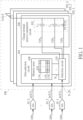
FIG. 1 is a diagram illustrating a compute-in-memory (CIM) circuit according to an embodiment of the present invention. -
FIG. 2 is a diagram illustrating a circuit design of a processing circuit used by the CIM circuit shown inFIG. 1 according to an embodiment of the present invention. -
FIG. 3 is a diagram illustrating calibration of different external analog buffers of a CIM circuit according to an embodiment of the present invention. -
FIG. 4 is a diagram illustrating inter-buffer mismatch between different external analog buffers. -
FIG. 5 is a diagram illustrating additional calibration of different external analog buffers of a CIM circuit according to an embodiment of the present invention. -
FIG. 6 is a diagram illustrating deviation between aligned transfer curves of different external analog buffers and an ideal curve before reference voltage tuning. -
FIG. 7 is a diagram illustrating that the aligned transfer curves of different external analog buffers are the same as the ideal curve after reference voltage tuning. -
FIG. 8 is a diagram illustrating per-layer calibration of different external analog buffers of a CIM circuit according to an embodiment of the present invention. - Certain terms are used throughout the following description and claims, which refer to particular components. As one skilled in the art will appreciate, electronic equipment manufacturers may refer to a component by different names. This document does not intend to distinguish between components that differ in name but not in function. In the following description and in the claims, the terms "include" and "comprise" are used in an open-ended fashion, and thus should be interpreted to mean "include, but not limited to ...". Also, the term "couple" is intended to mean either an indirect or direct electrical connection. Accordingly, if one device is coupled to another device, that connection may be through a direct electrical connection, or through an indirect electrical connection via other devices and connections.
-
FIG. 1 is a diagram illustrating a CIM circuit according to an embodiment of the present invention. TheCIM circuit 100 includes a plurality of processing circuits 102_1, 102_2, ..., 102_Z used to process a plurality of inputs, respectively. By way of example, but not limitation, the processing circuits 102_1-102_Z (Z ≥ 2) may have the same circuit architecture. Taking the processing circuit 102_1 for example, it may include a data-selection circuit 104 and a charge-domainpassive summation circuit 106. The data-selection circuit 104 may include amemory array 108 and aselection circuit 110. The charge-domainpassive summation circuit 106 may include aweighted capacitor array 112. As shown inFIG. 1 , theweighted capacitor array 112 includes a plurality of capacitors C1, C2, ..., CN with different capacitance values. Thememory array 108 includes a plurality ofmemory cells 114, and is arranged to store a plurality of candidate weights CW1, CW2, ..., CWY. Each of the candidate weights CW1-CWY (Y ≥ 2) may be an X-bit weight CWi[X-1:0] (i={1,2,...,Y} & X ≥ 2), and each bit of the X-bit weight CWi[X-1:0] is stored in onememory cell 114 of thememory array 108. For example, thememory array 108 may be a static random access memory (SRAM) array, and each of thememory cells 114 may be an SRAM cell. However, this is for illustrative purposes only, and is not meant to be a limitation of the present invention. In practice, the memory type of thememory array 108 may be adjusted, depending upon actual design considerations. - It should be noted that the present invention has no limitations on the arrangement of word lines (WLs) and bit lines (BLs) of the
memory array 108. In one exemplary implementation, thememory array 108 may be designed to have WLs in a horizontal direction and BLs in a vertical direction. In another exemplary implementation, thememory array 108 may be designed to have WLs in a vertical direction and BLs in a horizontal direction. - In some embodiments of the present invention, the
CIM circuit 100 may be an analog CIM (ACIM) circuit used by an artificial intelligence (AI) application, and the candidate weights CW1-CWY may be weights of a neural network such as a convolutional neural network (CNN) . Theselection circuit 110 is arranged to select a target weight Wk (k = {1,2,...,Z}) from the candidate weights CW1-CWY stored in the memory array108. For example, theselection circuit 110 of the processing circuit 102_1 may select a target weight W1 (i.e., Wk with k = 1) being one of the candidate weights CW1-CWY, theselection circuit 110 of another processing circuit 102_2 may select a target weight W2 (i.e., Wk with k = 2) being one of the candidate weights CW1-CWY, and theselection circuit 110 of yet another processing circuit 102_Z may select a target weight WZ (i.e., Wk with k = Z) being one of the candidate weights CW1-CWY. The target weights selected and used by different processing circuits 102_1-102_Z may be the same or may be different from each other. In a case where theCIM circuit 100 is used by an AI application, theCIM circuit 100 may be used to act as one neuron in the CNN, and may be reused to act as another neuron in the CNN. Hence, the candidate weights CW1-CWY may include weights of different neurons in the CNN. - In this embodiment, the
CIM circuit 100 is an ACIM circuit that uses the charge-domainpassive summation circuit 106 to generate an analog computation result of an analog input AOUT1 (i.e., AOUTk with k = 1) received by the processing circuit 102_1 and the target weight W1 (i.e., Wk with k = 1, which is one of the candidate weights CW1-CWY stored in the memory array 108) through theweighted capacitor array 112 with a particular capacitance ratio, where the particular capacitance ratio may be adjusted, depending upon actual design considerations. For example, capacitors C1-CN of theweighted capacitor array 112 may be implemented using MOM (Metal-Oxide-Metal) capacitors, and thus occupy a large layout area in a chip. In this embodiment, theweighted capacitor array 112 of the charge-domainpassive summation circuit 106 can be shared among multiple candidate weights CW1-CWY stored in thememory array 108. Hence, theweighted capacitor array 112 can be integrated with thememory array 108 for area optimization. Specifically, in a vertical direction of an integrated circuit, theweighted capacitor array 112 implemented using MOM capacitors may overlaymemory cells 114 of thememory array 108 that are used to store the candidate weights CW1-CWY. - In this embodiment, the processing circuits 102_1-102_Z are arranged to receive a plurality of analog inputs AOUT1, AOUT2, ..., AOUTZ output from a plurality of external analog buffers 10_1, 10_2, 10_Z, respectively. For example, each of the external analog buffers 10_1-10_Z may be implemented using a digital-to-analog converter (labeled by "DA") . Hence, the analog inputs AOUT1, AOUT2, ..., AOUTZ are generated by converting a plurality of digital codes DIN1, DIN2, ..., DINZ from a digital domain to an analog domain. Since inputs of the processing circuits 102_1-102_Z are analog signals, node (energy) reduction can be achieved. For example, the processing circuit 102_1 requires only a single node N_IN for receiving only a single analog input AOUT1 (which has a specific voltage level representative of the digital code DIN1) from the external analog buffer 10_1, such that the input power dissipation (fCV2) can be greatly reduced.
- As mentioned above, each of the candidate weights CW1-CWY (Y ≥ 2) may be an X-bit weight CWi[X-1:0] (i={1,2,...,Y} & X ≥ 2), and each bit of the X-bit weight CWi[X-1:0] is stored in one
memory cell 114 of thememory array 108. Hence, the target weight W1 (i.e., Wk with k = 1) has a plurality of bits W1[X-1:0] stored inmemory cells 114 in thememory array 108, respectively. In this embodiment, theselection circuit 110 is further arranged to selectively apply the analog input AOUT1 to capacitors C1-CN according to bits W1[X-1:0], respectively. For example, theweighted capacitor array 112 is a binary-weighted capacitor array (N = X-1) consisting of capacitors CN = 2X-1C, ..., C2 = 2C, and C1 = 1C. When W1 [i] (i = {1,2,...,X - 1}) is equal to 1, theselection circuit 110 allows the analog input AOUT1 to be delivered to a capacitor Ci of the binary-weighted capacitor array 112 (i.e., VINi = AOUT1). When W1[i] (i = {1,2,...,X - 1}) is equal to 0, theselection circuit 110 blocks the analog input AOUT1 from being delivered to the capacitor Ci of the binary-weightedcapacitor array 112, and allows a reference voltage (e.g., ground voltage GND) to be delivered to the capacitor Ci of the binary-weighted capacitor array 112 (i.e., VINi = GND). In this embodiment, theselection circuit 110 is arranged to control transmission of the analog input AOUT1 by referring to the bits W1[X-1:0] concurrently, thereby enabling a direct multi-bit operation for setting the analog computation result at the charge-domainpassive summation circuit 106. Hence, the charge-domain passive summation circuit 106 (particularly,weighted capacitor array 112 of charge-domain passive summation circuit 106) of the processing circuit 102_1 generates an analog computation result (which is an analog output of DIN 1 × W 1[X - 1:0]) by combining the voltage signals VIN1-VINN through charge redistribution among the binary-weighted capacitor array CN = 2X-1C, ..., C2 = 2C, and C1 = 1C. Since the analog computation result is set by controlling voltage signals VIN1-VINN applied to capacitors C1-CN of theweighted capacitor array 112 according to bits W1[X-1:0], the analog computation result with high accuracy can be generated from the processing circuit 102_1. - Similarly, the charge-domain passive summation circuit 106 (particularly,
weighted capacitor array 112 of charge-domain passive summation circuit 106) of anther processing circuit 102_2 generates an analog computation result (which is an analog output of DIN 2 × W 2[X - 1:0]) by combining the voltage signals VIN1-VINN through charge redistribution among the binary-weighted capacitor array CN = 2X-1C, ..., C2 = 2C, and C1 = 1C; and the charge-domain passive summation circuit 106 (particularly,weighted capacitor array 112 of charge-domain passive summation circuit 106) of yet another processing circuit 102_Z generates an analog computation result (which is an analog output of DINZ × WZ [X - 1:0]) by combining the voltage signals VIN1-VINN through charge redistribution among the binary-weighted capacitor array CN = 2X-1C, ..., C2 = 2C, and C1 = 1C. - As shown in
FIG. 1 , each of the capacitors C1-CN has a top plate P1 and a bottom plate P2, and top plates P1 of capacitors C1-CN included in theweighted capacitor arrays 112 of all processing circuits 102_1-102_Z are directly connected without selection. The output voltage VOUT (which is an analog output of
- For better comprehension of technical features of the present invention, an exemplary circuit design of a processing circuit used by the proposed
CIM circuit 100 is illustrated inFIG. 2 . The processing circuit 102_k ( k = {1,2,...,Z}) shown inFIG. 2 may be any of the processing circuits 102_1-102_Z shown inFIG. 1 . In this embodiment, the candidate weights CW1-CWY may be stored in memory cell lines (e.g., memory cell rows or memory cell columns), respectively; and candidate weights included in the candidate weights CW1-CWY that are not selected as the target weight Wk used by the processing circuit 102_k are collectively represented by Wj. Theselection circuit 110 may be a switch-based circuit including a plurality of switches that may be implemented using P-channel metal-oxide-semiconductor (PMOS) transistors or N-channel metal-oxide-semiconductor (NMOS) transistors, and may be integrated with thememory array 108. As shown inFIG. 2 , theselection circuit 110 includes a plurality of global selection switches SWk and SWj, where the global selection switch SWk corresponds to a candidate weight that is selected as the target weight Wk, and the global selection switch SWj corresponds to any candidate weight that is not selected as the target weight Wk. Specifically, the global selection switch SWk is shared among memory cells that store bits of a candidate weight that is selected as the target weight Wk, and the global selection switch SWj is shared among memory cells that store bits of a candidate weight that is not selected as the target weight Wk. In addition, theselection circuit 110 includes a plurality of local selection switches for each memory cell that stores one bit of the candidate weights CW1-CWY. Taking the memory cell that stores the bit Wk[X-1] for example, there are two weight switches SW1 and SW2 and one cell switch SW3. However, this is for illustrative purposes only, and is not meant to be a limitation of the present invention. In practice, the number of local selection switches for each memory cell may be adjusted, depending upon actual design considerations. - Each of the global selection switches SWk and SWj has one terminal that is arranged to receive the analog input AOUTk from an external analog buffer (not shown). One of the global selection switches that corresponds to a memory cell line (e.g., memory cell row or memory cell column) in which the target weight Wk is stored is switched on, and the rest of the global selection switches are switched off. In this embodiment, one switch control signal W_ADD_ENk may be asserted to switch on the global selection switch SWk, and another switch control signal W_ADD_ENj may be deasserted to switch off the global selection switch SWj. Though the candidate weight Wj is not selected as the target weight Wk, the memory cells that store bits of the candidate weight Wj may include input parasitic capacitance Cpar_in. By switching off the global selection switch SWj, the power dissipation resulting from input parasitic capacitance Cpar_in of memory cells that stores bits of the candidate weight Wj can be prevented to achieve energy reduction/power saving.
- Suppose that the
memory array 108 is an SRAM array, and each of thememory cells 114 is an SRAM cell. Hence, eachmemory cell 114 may have two bit lines BL andBL , where a voltage level at the bit line BL (which is labeled by "+" inFIG. 2 ) is set based on the bit stored in thememory cell 114, and a voltage level at the bit line BL (which is labeled by "-" inFIG. 2 ) is set based on an inverse of the bit stored in thememory cell 114. Regarding a memory cell that stores one bit of the target weight Wk, the weight switches SW1 and SW2 (which are local selection switches of the memory cell) are controlled by the bit stored in the memory cell. Taking the weight switches SW1 and SW2 of the memory cell that stores the bit Wk[X-1] for example, the weight switch SW1 is controlled by the bit Wk[X-1], and the weight switch SW2 is controlled by an inverse of the bit Wk[X-1] (i.e.,Wk [X - 1] ), where the weight switch SW1 determines whether the analog input AOUTk (which is received from the switched-on global selection switch SWk) is passed to the charge-domain passive summation circuit (particularly,capacitor 2X-1C of weighted capacitor array 112), and the weight switch SW2 determines whether a reference voltage (e.g., ground voltage) is passed to the charge-domain passive summation circuit (particularly,capacitor 2X-1C of weighted capacitor array 112). It should be noted that the weight switches SW1 and SW2 are not switched on at the same time. That is, the weight switch SW2 is switched off during a period in which the weight switch SW1 is switched on, and the weight switch SW1 is switched off during a period in which the weight switch SW2 is switched on. - The cell selection switch SW3 is also a local selection switch integrated with each
memory cell 114. In this embodiment, the candidate weights CW1-CWY may be stored in memory cell lines (e.g., memory cell rows or memory cell columns), respectively. The cell selection switches SW3 integrated with thememory array 108 may be categorized into a plurality of cell selection switch groups that correspond to the memory cell lines (e.g., memory cell rows or memory cell columns), respectively. Hence, each of the cell selection switch groups includes cell selection switches SW3, each having one terminal that is coupled to the charge-domain passive summation circuit (particularly, one capacitor of weighted capacitor array 122). For example, the cell selection switch SW3 of the memory cell that stores the bit Wk[X-1] has one terminal coupled to thecapacitor 2X-1C of theweighted capacitor array 112, the cell selection switch SW3 of the memory cell that stores the bit Wk[0] has one terminal coupled to thecapacitor 1C of theweighted capacitor array 112, and so on. In this embodiment, cell selection switches of one of the cell selection switch groups that corresponds to a memory cell line (e.g., memory cell row or memory cell column) in which the target weight Wk is stored are switched on, and cell selection switches of the rest of the cell selection switch groups are switched off. For example, cell selection switches SW3 of a cell selection switch group that corresponds to a memory cell line (e.g., memory cell row or memory cell column) in which the candidate weight Wj is stored are switched off. Though the candidate weight Wj is not selected as the target weight Wk, the memory cells that store bits of the candidate weight Wj may include cell parasitic capacitance Cpar_cell. By switching off the cell selection switches SW3, the power dissipation resulting from cell parasitic capacitance Cpar_cell of memory cells that stores bits of the candidate weight Wj (which is not selected as the target weight Wk) can be prevented to achieve energy reduction/power saving. - As shown in
FIG. 1 , the external analog buffers (e.g., digital-to-analog converters) 10_1-10_Z generates analog inputs AOUT1-AOUTZ of the processing circuits 102_1-102_Z, respectively. Ideally, when two digital codes (e.g., DIN1 and DIN2) are the same, the corresponding analog inputs (e.g., AOUT1 and AOUT2) received by theCIM circuit 100 should be the same. However, inter-buffer mismatch may exist between different analog buffers due to imperfection of circuit components. As a result, the output voltage VOUT (which is an analog output of
CIM circuit 100 is used by an AI application, the classification accuracy may be degraded due to the inter-buffer mismatch. To address this issue, theCIM circuit 100 is further involved in calibration of external analog buffers (e.g., digital-to-analog converters) 10_1-10_Z. - Please refer to
FIG. 3 andFIG. 4 .FIG. 3 is a diagram illustrating calibration of different external analog buffers of a CIM circuit according to an embodiment of the present invention.FIG. 4 is a diagram illustrating inter-buffer mismatch between different external analog buffers. Theexternal analog buffer 301 may be one of the external analog buffers (e.g., digital-to-analog converters) 10_1-10_Z shown inFIG. 1 . Theexternal analog buffer 302 may be another of the external analog buffers (e.g., digital-to-analog converters) 10_1-10_Z shown inFIG. 1 . Due to imperfection of circuit components, the transfer curve CV1 of theexternal analog buffer 301 is different from the transfer curve CV2 of theexternal analog buffer 302. Hence, the calibration of the external analog buffers 301 and 302 may include cancelling inter-buffer mismatch between the external analog buffers 301 and 302. For example, an auto-zeroing technique may be employed for inter-buffer mismatch cancellation. In some embodiments of the present invention, each of the external analog buffers 301 and 302 may be a discrete-time buffer. The discrete-time operation of theexternal analog buffer 301/302 may include a first phase in which theexternal analog buffer 301/302 operates in a reset (RST) mode and a second phase in which theexternal analog buffer 301/302 operates in a buffer (BUF) mode. The calibration of the external analog buffers 301 and 302 is performed during a period in which both of the external analog buffers 301 and 302 operate in the RST mode. As shown inFIG. 3 , the same digital input (e.g., digital code = 0) is fed into both of the external analog buffers 301 and 302, and a ground voltage is applied to top plates of capacitors included in theweighted capacitor array 112. In this way, the inter-buffer mismatch between the external analog buffers 301 and 302 is stored in theweighted capacitor array 112 when the external analog buffers 301 and 302 operate in the RST mode, and can be subtracted from the output voltage VOUT (which is an analog output of
- However, it is possible that the same transfer curve possessed by the external analog buffers 301 and 302 after auto-zeroing may still deviate from an ideal curve. To address this issue, the calibration of the external analog buffers 301 and 302 may further include aligning a transfer curve of each of the external analog buffers 301 and 302 with a predetermined curve.
- Please refer to
FIG. 5 ,FIG. 6 , andFIG. 7 .FIG. 5 is a diagram illustrating additional calibration of different external analog buffers of a CIM circuit according to an embodiment of the present invention.FIG. 6 is a diagram illustrating deviation between aligned transfer curves of the external analog buffers 301 and 302 and an ideal curve CV' before reference voltage tuning.FIG. 7 is a diagram illustrating that the aligned transfer curves of the external analog buffers 301 and 302 are the same as the ideal curve CV' after reference voltage tuning. The minimum digital input (e.g., minimum code min) is applied to the external analog buffers 301 and 302, and a global offset E1 is obtained by theADC 304, where a bias voltage Vbias of theADC 304 is generated from a reference voltage generator. In addition, the maximum digital input (e.g., maximum code max) is applied to the external analog buffers 301 and 302, and a gain error E2 is obtained by theADC 304. As shown inFIG. 5 , reference voltage generator calibration (labeled by "Vref Gen Calibration") is performed for tuning the reference voltages Vref used by the external analog buffers 301 and 302. In this way, the external analog buffers 301 and 302 can have the same transfer curve (which results from auto-zeroing) aligned with the ideal curve CV' through reference voltage tuning. - As mentioned above, the proposed
CIM circuit 100 may be employed by an AI application. For example, the AI application may employ a CNN with multiple layers, and the proposedCIM circuit 100 may be used by a neuron in one layer and reused by a neuron in another layer. In some embodiments of the present invention, per-layer calibration may be employed for tracking process, voltage, temperature (PVT) variation.FIG. 8 is a diagram illustrating per-layer calibration of different external analog buffers of a CIM circuit according to an embodiment of the present invention. In this embodiment, the neural network includes a plurality of layers such as L1, L2, and L3 shown inFIG. 8 . Thesame CIM circuit 100 may be shared among different layers L1, L2, and L3. The aforementioned calibration (labeled by "ReK") of different external analog buffers (e.g., external analog buffers 301 and 302 shown inFIG. 3 andFIG. 5 ) is performed per layer, thereby making the external analog buffers 301 and 302 have the same transfer curve aligned with the ideal curve CV'. With the help of the per-layer calibration, a PVT insensitive ACIM circuit can be achieved. - Those skilled in the art will readily observe that numerous modifications and alterations of the device and method may be made while retaining the teachings of the invention. Accordingly, the above disclosure should be construed as limited only by the metes and bounds of the appended claims.
- The present invention may also be defined by the following numbered clauses.
- 1. A compute-in-memory (CIM) circuit comprising:
a first processing circuit, comprising:- a first data-selection circuit, comprising:
- a first memory array, arranged to store a plurality of candidate weights; and
- a first selection circuit, arranged to select a first target weight from the plurality of candidate weights stored in the first memory array; and
- a first charge-domain passive summation circuit, arranged to generate a first analog computation result of a first input received by the first processing circuit and the first target weight stored in the first memory array through a first weighted capacitor array integrated with the first memory array.
- a first data-selection circuit, comprising:
- 2. The CIM circuit of
clause 1, wherein the plurality of candidate weights are weights of a neural network. - 3. The CIM circuit of
clause 1, wherein the first input of the first processing circuit is a single analog signal generated from an external analog buffer. - 4. The CIM circuit of
clause 1, wherein the first target weight comprises a plurality of bits, and the plurality of bits are stored in a plurality of memory cells in the memory array, respectively. - 5. The CIM circuit of clause 4, wherein the first weighted capacitor array comprises a plurality of capacitors; and the first selection circuit is further arranged to selectively apply the first input to the plurality of capacitors according to the plurality of bits, respectively.
- 6. The CIM circuit of clause 5, wherein the first selection circuit is further arranged to control transmission of the first input by referring to the plurality of bits concurrently.
- 7. The CIM circuit of
clause 1, further comprising:- a second data-selection circuit, comprising:
- a second memory array, arranged to store the plurality of candidate weights; and
- a second selection circuit, arranged to select a second target weight from the plurality of candidate weights stored in the second memory array; and
- a second charge-domain passive summation circuit, arranged to generate a second analog computation result of a second input received by the second processing circuit and the second target weight stored in the second memory array through a second weighted capacitor array integrated with the second memory array;
- wherein the first weighted capacitor array comprises a plurality of first capacitors each having a first plate and a second plate;
- the second weighted capacitor array comprises a plurality of second capacitors each having a first plate and a second plate; and first plates of the plurality of first capacitors are connected to first plates of the second capacitors.
- a second data-selection circuit, comprising:
- 8. The CIM circuit of clause 7, wherein the plurality of candidate weights are weights of a neural network.
- 9. The CIM circuit of
clause 1, wherein the first weighted capacitor array of the first charge-domain passive summation circuit is shared among the plurality of candidate weights stored in the first memory array. - 10. The CIM circuit of
clause 1, wherein the first memory array comprises a plurality of memory cell lines arranged to store the plurality of candidate weights, respectively; the first selection circuit comprises:
a plurality of global selection switches, corresponding to the plurality of memory cell lines, respectively, wherein each of the plurality of global selection switches has one terminal that is arranged to receive the first input, and one of the plurality of global selection switches that corresponds to a memory cell line in which the first target weight is stored is switched on. - 11. The CIM circuit of clause 10, wherein the rest of the plurality of global selection switches are switched off.
- 12. The CIM circuit of
clause 1, wherein the plurality of memory cells comprise a plurality of first memory cells arranged to store a plurality of bits of the first target weight; and for each of the plurality of bits of the first target weight, the first selection circuit comprises:- a first switch, controlled by the bit, wherein the first switch determines whether the first input is passed to the first charge-domain passive summation circuit; and
- a second switch, controlled by an inverse of the bit, wherein the second switch determines whether a reference voltage is passed to the first charge-domain passive summation circuit.
- 13. The CIM circuit of
clause 1, wherein the first memory array comprises a plurality of memory cell lines arranged to store the plurality of candidate weights, respectively; the first selection circuit comprises:
a plurality of cell selection switch groups, corresponding to the plurality of memory cell lines, respectively, wherein each of the plurality of cell selection switch groups comprises cell selection switches, each having one terminal that is coupled to the first charge-domain passive summation circuit; and cell selection switches of one of the plurality of cell selection switch groups that corresponds to a memory cell line in which the first target weight is stored are switched on. - 14. The CIM circuit of clause 13, wherein cell selection switches of the rest of the plurality of cell selection switch groups are switched off.
- 15. The CIM circuit of
clause 1, further comprising:- a second data-selection circuit, comprising:
- a second memory array, arranged to store the plurality of candidate weights; and
- a second selection circuit, arranged to select a second target weight from the plurality of candidate weights stored in the second memory array; and
- a second charge-domain passive summation circuit, arranged to generate a second analog computation result of a second input received by the second data-selection circuit and the second target weight stored in the second memory array through a second weighted capacitor array integrated with the second memory array;
- wherein the first data-selection circuit receives the first input from a first external analog buffer, and the second data-selection circuit receives the second input from a second external analog buffer; and
- wherein the CIM circuit is further involved in calibration of the first external analog buffer and the second external analog buffer.
- a second data-selection circuit, comprising:
- 16. The CIM circuit of clause 15, wherein the calibration of the first external analog buffer and the second external analog buffer comprises cancelling inter-buffer mismatch between the first external analog buffer and the second external analog buffer.
- 17. The CIM circuit of clause 16, wherein the calibration of the first external analog buffer and the second external analog buffer further comprises aligning a transfer curve of each of the first external analog buffer and the second external analog buffer with a predetermined curve.
- 18. The CIM circuit of clause 15, wherein a neural network includes a plurality of layers, the CIM circuit is used by each of the plurality of layers, and the calibration of the first external analog buffer and the second external analog buffer is performed per layer.
- 19. A compute-in-memory (CIM) method comprising:
- storing a plurality of candidate weights in a memory array;
- selecting a target weight from the plurality of candidate weights; and
- performing, by a weighted capacitor array integrated with the memory array, charge-domain passive summation to generate an analog computation result of an input and the target weight.
- 20. The CIM method of clause 19, wherein the plurality of candidate weights are weights of a neural network.
Claims (15)
- A compute-in-memory, CIM, circuit comprising:
a first processing circuit (102_1-102_z), comprising:a first data-selection circuit (104), comprising:a first memory array (108), arranged to store a plurality of candidate weights; anda first selection circuit (110), arranged to select a first target weight from the plurality of candidate weights stored in the first memory array (108); anda first charge-domain passive summation circuit (106), arranged to generate a first analog computation result of a first input received by the first processing circuit (102_1-102_z) and the first target weight stored in the first memory array (108) through a first weighted capacitor array (112, 122) integrated with the first memory array (108). - The CIM circuit (100) of claim 1, wherein the plurality of candidate weights are weights of a neural network.
- The CIM circuit (100) of claim 1 or claim 2, wherein the first input of the first processing circuit (102_1-102_z) is a single analog signal generated from an external analog buffer (10_1-10-z, 301, 302).
- The CIM circuit (100) of any one of the preceding claims, wherein the first target weight comprises a plurality of bits, and the plurality of bits are stored in a plurality of memory cells (114) in the memory array (108), respectively.
- The CIM circuit (100) of claim 4, wherein the first weighted capacitor array (112, 122) comprises a plurality of capacitors; and the first selection circuit (110) is further arranged to selectively apply the first input to the plurality of capacitors according to the plurality of bits, respectively.
- The CIM circuit (100) of claim 5, wherein the first selection circuit (110) is further arranged to control transmission of the first input by referring to the plurality of bits concurrently.
- The CIM circuit (100) of claim 1, further comprising:a second data-selection circuit (104), comprising:a second memory array (108), arranged to store the plurality of candidate weights; anda second selection circuit (110), arranged to select a second target weight from the plurality of candidate weights stored in the second memory array (108); anda second charge-domain passive summation circuit (106), arranged to generate a second analog computation result of a second input received by the second processing circuit (102_1-102_z and the second target weight stored in the second memory array (108) through a second weighted capacitor array (112, 122) integrated with the second memory array (108);wherein the first weighted capacitor array (112, 122) comprises a plurality of first capacitors each having a first plate and a second plate; the second weighted capacitor array (112, 122) comprises a plurality of second capacitors each having a first plate and a second plate; and first plates of the plurality of first capacitors are connected to first plates of the second capacitors.
- The CIM circuit (100) of any one of the preceding claims, wherein the first weighted capacitor array (112, 122) of the first charge-domain passive summation circuit (106) is shared among the plurality of candidate weights stored in the first memory array (108) .
- The CIM circuit (100) of any one of the preceding claims, wherein the first memory array (108) comprises a plurality of memory cell (114) lines arranged to store the plurality of candidate weights, respectively; the first selection circuit (110) comprises:
a plurality of global selection switches, corresponding to the plurality of memory cell (114) lines, respectively, wherein each of the plurality of global selection switches has one terminal that is arranged to receive the first input, and one of the plurality of global selection switches that corresponds to a memory cell (114) line in which the first target weight is stored is switched on. - The CIM circuit (100) of claim 1, wherein the plurality of memory cells (114) comprise a plurality of first memory cells (114) arranged to store a plurality of bits of the first target weight; and for each of the plurality of bits of the first target weight, the first selection circuit (110) comprises:a first switch, controlled by the bit, wherein the first switch determines whether the first input is passed to the first charge-domain passive summation circuit (106); anda second switch, controlled by an inverse of the bit, wherein the second switch determines whether a reference voltage is passed to the first charge-domain passive summation circuit (106).
- The CIM circuit (100) of claim 1, wherein the first memory array (108) comprises a plurality of memory cell (114) lines arranged to store the plurality of candidate weights, respectively; the first selection circuit (110) comprises:
a plurality of cell selection switch groups, corresponding to the plurality of memory cell (114) lines, respectively, wherein each of the plurality of cell selection switch groups comprises cell selection switches, each having one terminal that is coupled to the first charge-domain passive summation circuit (106); and cell selection switches of one of the plurality of cell selection switch groups that corresponds to a memory cell (114) line in which the first target weight is stored are switched on. - The CIM circuit (100) of claim 1, further comprising:a second data-selection circuit (104), comprising:a second memory array (108), arranged to store the plurality of candidate weights; anda second selection circuit (110), arranged to select a second target weight from the plurality of candidate weights stored in the second memory array (108); anda second charge-domain passive summation circuit (106), arranged to generate a second analog computation result of a second input received by the second data-selection circuit (104) and the second target weight stored in the second memory array (108) through a second weighted capacitor array (112, 122) integrated with the second memory array (108);wherein the first data-selection circuit (104) receives the first input from a first external analog buffer (10_1-10-z, 301, 302), and the second data-selection circuit (104) receives the second input from a second external analog buffer (10_1-10-z, 301, 302); andwherein the CIM circuit (100) is further involved in calibration of the first external analog buffer (10_1-10-z, 301, 302)and the second external analog buffer (10_1-10-z, 301, 302).
- The CIM circuit (100) of claim 15, wherein the calibration of the first external analog buffer (10_1-10-z, 301, 302)and the second external analog buffer (10_1-10-z, 301, 302)comprises cancelling inter-buffer mismatch between the first external analog buffer (10_1-10-z, 301, 302)and the second external analog buffer (10_1-10-z, 301, 302); or
wherein the calibration of the first external analog buffer (10_1-10-z, 301, 302)and the second external analog buffer (10_1-10-z, 301, 302)further comprises aligning a transfer curve of each of the first external analog buffer (10_1-10-z, 301, 302)and the second external analog buffer (10_1-10-z, 301, 302)with a predetermined curve. - The CIM circuit (100) of claim 15, wherein a neural network includes a plurality of layers, the CIM circuit (100) is used by each of the plurality of layers, and the calibration of the first external analog buffer (10_1-10-z, 301, 302)and the second external analog buffer (10_1-10-z, 301, 302)is performed per layer.
- A compute-in-memory, CIM, method comprising:storing a plurality of candidate weights in a memory array (108);selecting a target weight from the plurality of candidate weights; andperforming, by a weighted capacitor array (112, 122) integrated with the memory array (108), charge-domain passive summation to generate an analog computation result of an input and the target weight.
Applications Claiming Priority (3)
| Application Number | Priority Date | Filing Date | Title |
|---|---|---|---|
| US202263369674P | 2022-07-28 | 2022-07-28 | |
| US202263369673P | 2022-07-28 | 2022-07-28 | |
| US18/215,175 US20240037178A1 (en) | 2022-07-28 | 2023-06-28 | Compute-in-memory circuit with charge-domain passive summation and associated method |
Publications (2)
| Publication Number | Publication Date |
|---|---|
| EP4312217A1 true EP4312217A1 (en) | 2024-01-31 |
| EP4312217B1 EP4312217B1 (en) | 2026-04-01 |
Family
ID=87280250
Family Applications (1)
| Application Number | Title | Priority Date | Filing Date |
|---|---|---|---|
| EP23187131.0A Active EP4312217B1 (en) | 2022-07-28 | 2023-07-23 | Compute-in-memory circuit with charge-domain passive summation and associated method |
Country Status (3)
| Country | Link |
|---|---|
| US (1) | US20240037178A1 (en) |
| EP (1) | EP4312217B1 (en) |
| TW (1) | TWI881408B (en) |
Families Citing this family (1)
| Publication number | Priority date | Publication date | Assignee | Title |
|---|---|---|---|---|
| US20250111215A1 (en) * | 2023-09-28 | 2025-04-03 | Mediatek Inc. | Configurable computing-in-memory (cim) for power control |
Citations (1)
| Publication number | Priority date | Publication date | Assignee | Title |
|---|---|---|---|---|
| US20220012016A1 (en) * | 2021-09-24 | 2022-01-13 | Intel Corporation | Analog multiply-accumulate unit for multibit in-memory cell computing |
Family Cites Families (2)
| Publication number | Priority date | Publication date | Assignee | Title |
|---|---|---|---|---|
| CN115461712A (en) * | 2020-02-05 | 2022-12-09 | 普林斯顿大学理事会 | Scalable array architecture for in-memory computation |
| US11705171B2 (en) * | 2021-09-23 | 2023-07-18 | Intel Corporation | Switched capacitor multiplier for compute in-memory applications |
-
2023
- 2023-06-28 US US18/215,175 patent/US20240037178A1/en active Pending
- 2023-07-23 EP EP23187131.0A patent/EP4312217B1/en active Active
- 2023-07-28 TW TW112128437A patent/TWI881408B/en active
Patent Citations (1)
| Publication number | Priority date | Publication date | Assignee | Title |
|---|---|---|---|---|
| US20220012016A1 (en) * | 2021-09-24 | 2022-01-13 | Intel Corporation | Analog multiply-accumulate unit for multibit in-memory cell computing |
Also Published As
| Publication number | Publication date |
|---|---|
| TW202420117A (en) | 2024-05-16 |
| EP4312217B1 (en) | 2026-04-01 |
| US20240037178A1 (en) | 2024-02-01 |
| TWI881408B (en) | 2025-04-21 |
Similar Documents
| Publication | Publication Date | Title |
|---|---|---|
| CN101807923B (en) | Hybrid Analog-to-Digital Converter | |
| EP2697905B1 (en) | Self timed digital-to-analog converter | |
| US5235335A (en) | Circuit and method for tuning capacitor arrays | |
| US8659459B2 (en) | Digital-to-analog converter, analog-to-digital converter including same, and semiconductor device | |
| US20110234433A1 (en) | A/d converter | |
| US9698813B2 (en) | Input buffer and analog-to-digital converter | |
| US10979065B1 (en) | Signal processing circuit, in-memory computing device and control method thereof | |
| TW201141072A (en) | Capacitive voltage divider | |
| US12224766B2 (en) | Analog digital converter and method for analog to digital converting in the analog digital converter | |
| EP4312217B1 (en) | Compute-in-memory circuit with charge-domain passive summation and associated method | |
| US6633249B1 (en) | Low power, scalable analog to digital converter having circuit for compensating system non-linearity | |
| US12062411B2 (en) | Semiconductor device performing a multiplication and accumulation operation | |
| US20230370082A1 (en) | Shared column adcs for in-memory-computing macros | |
| US7429945B2 (en) | Analog to digital converter | |
| US20230385620A1 (en) | Spike neural network circuit | |
| US5719576A (en) | Capacitor array digital/analog converter with compensation array for stray capacitance | |
| JPH0519848B2 (en) | ||
| US20060244647A1 (en) | Digital-to-analog converter and successive approximation type analog-to-digital converter utilizing the same | |
| US12418297B2 (en) | Capacitor weighted segmentation buffer | |
| CN117476060A (en) | Storage and calculation integrated circuit with charge domain passive summation circuit and related methods | |
| US20190190534A1 (en) | Quantizer including capacitors and operating method of quantizer | |
| US20210266008A1 (en) | Two-capacitor digital-to-analog converter | |
| JP2009278169A (en) | Capacitor array circuit, and semiconductor device and successive approximation a/d converter using the same | |
| US20240176587A1 (en) | Multi-bit analog multiplication and accumulation circuit system | |
| KR102967870B1 (en) | Shared columns for in-memory computing macros |
Legal Events
| Date | Code | Title | Description |
|---|---|---|---|
| PUAI | Public reference made under article 153(3) epc to a published international application that has entered the european phase |
Free format text: ORIGINAL CODE: 0009012 |
|
| STAA | Information on the status of an ep patent application or granted ep patent |
Free format text: STATUS: THE APPLICATION HAS BEEN PUBLISHED |
|
| AK | Designated contracting states |
Kind code of ref document: A1 Designated state(s): AL AT BE BG CH CY CZ DE DK EE ES FI FR GB GR HR HU IE IS IT LI LT LU LV MC ME MK MT NL NO PL PT RO RS SE SI SK SM TR |
|
| STAA | Information on the status of an ep patent application or granted ep patent |
Free format text: STATUS: REQUEST FOR EXAMINATION WAS MADE |
|
| 17P | Request for examination filed |
Effective date: 20240731 |
|
| RBV | Designated contracting states (corrected) |
Designated state(s): AL AT BE BG CH CY CZ DE DK EE ES FI FR GB GR HR HU IE IS IT LI LT LU LV MC ME MK MT NL NO PL PT RO RS SE SI SK SM TR |
|
| GRAP | Despatch of communication of intention to grant a patent |
Free format text: ORIGINAL CODE: EPIDOSNIGR1 |
|
| STAA | Information on the status of an ep patent application or granted ep patent |
Free format text: STATUS: GRANT OF PATENT IS INTENDED |
|
| RIC1 | Information provided on ipc code assigned before grant |
Ipc: G11C 7/10 20060101AFI20250926BHEP Ipc: G06N 3/02 20060101ALI20250926BHEP Ipc: G11C 11/54 20060101ALI20250926BHEP Ipc: G11C 27/02 20060101ALI20250926BHEP Ipc: G06N 3/0464 20230101ALI20250926BHEP Ipc: G06N 3/065 20230101ALI20250926BHEP |
|
| INTG | Intention to grant announced |
Effective date: 20251029 |
|
| GRAS | Grant fee paid |
Free format text: ORIGINAL CODE: EPIDOSNIGR3 |
|
| GRAA | (expected) grant |
Free format text: ORIGINAL CODE: 0009210 |
|
| STAA | Information on the status of an ep patent application or granted ep patent |
Free format text: STATUS: THE PATENT HAS BEEN GRANTED |
|
| AK | Designated contracting states |
Kind code of ref document: B1 Designated state(s): AL AT BE BG CH CY CZ DE DK EE ES FI FR GB GR HR HU IE IS IT LI LT LU LV MC ME MK MT NL NO PL PT RO RS SE SI SK SM TR |
|
| REG | Reference to a national code |
Ref country code: CH Ref legal event code: F10 Free format text: ST27 STATUS EVENT CODE: U-0-0-F10-F00 (AS PROVIDED BY THE NATIONAL OFFICE) Effective date: 20260401 Ref country code: GB Ref legal event code: FG4D |
|
| PGFP | Annual fee paid to national office [announced via postgrant information from national office to epo] |
Ref country code: FR Payment date: 20260331 Year of fee payment: 4 |
|
| REG | Reference to a national code |
Ref country code: IE Ref legal event code: FG4D |
|
| REG | Reference to a national code |
Ref country code: DE Ref legal event code: R096 Ref document number: 602023014354 Country of ref document: DE |