EP4311042A1 - Opto-electronic device - Google Patents
Opto-electronic device Download PDFInfo
- Publication number
- EP4311042A1 EP4311042A1 EP22306085.6A EP22306085A EP4311042A1 EP 4311042 A1 EP4311042 A1 EP 4311042A1 EP 22306085 A EP22306085 A EP 22306085A EP 4311042 A1 EP4311042 A1 EP 4311042A1
- Authority
- EP
- European Patent Office
- Prior art keywords
- zone
- junction
- taper
- iii
- layer
- Prior art date
- Legal status (The legal status is an assumption and is not a legal conclusion. Google has not performed a legal analysis and makes no representation as to the accuracy of the status listed.)
- Granted
Links
Images









Classifications
-
- H—ELECTRICITY
- H01—ELECTRIC ELEMENTS
- H01S—DEVICES USING THE PROCESS OF LIGHT AMPLIFICATION BY STIMULATED EMISSION OF RADIATION [LASER] TO AMPLIFY OR GENERATE LIGHT; DEVICES USING STIMULATED EMISSION OF ELECTROMAGNETIC RADIATION IN WAVE RANGES OTHER THAN OPTICAL
- H01S5/00—Semiconductor lasers
- H01S5/02—Structural details or components not essential to laser action
- H01S5/0206—Substrates, e.g. growth, shape, material, removal or bonding
- H01S5/0207—Substrates having a special shape
-
- H—ELECTRICITY
- H01—ELECTRIC ELEMENTS
- H01S—DEVICES USING THE PROCESS OF LIGHT AMPLIFICATION BY STIMULATED EMISSION OF RADIATION [LASER] TO AMPLIFY OR GENERATE LIGHT; DEVICES USING STIMULATED EMISSION OF ELECTROMAGNETIC RADIATION IN WAVE RANGES OTHER THAN OPTICAL
- H01S5/00—Semiconductor lasers
- H01S5/02—Structural details or components not essential to laser action
- H01S5/0206—Substrates, e.g. growth, shape, material, removal or bonding
-
- H—ELECTRICITY
- H01—ELECTRIC ELEMENTS
- H01S—DEVICES USING THE PROCESS OF LIGHT AMPLIFICATION BY STIMULATED EMISSION OF RADIATION [LASER] TO AMPLIFY OR GENERATE LIGHT; DEVICES USING STIMULATED EMISSION OF ELECTROMAGNETIC RADIATION IN WAVE RANGES OTHER THAN OPTICAL
- H01S5/00—Semiconductor lasers
- H01S5/02—Structural details or components not essential to laser action
- H01S5/028—Coatings ; Treatment of the laser facets, e.g. etching, passivation layers or reflecting layers
- H01S5/0285—Coatings with a controllable reflectivity
-
- H—ELECTRICITY
- H01—ELECTRIC ELEMENTS
- H01S—DEVICES USING THE PROCESS OF LIGHT AMPLIFICATION BY STIMULATED EMISSION OF RADIATION [LASER] TO AMPLIFY OR GENERATE LIGHT; DEVICES USING STIMULATED EMISSION OF ELECTROMAGNETIC RADIATION IN WAVE RANGES OTHER THAN OPTICAL
- H01S5/00—Semiconductor lasers
- H01S5/10—Construction or shape of the optical resonator, e.g. extended or external cavity, coupled cavities, bent-guide, varying width, thickness or composition of the active region
- H01S5/1053—Comprising an active region having a varying composition or cross-section in a specific direction
- H01S5/106—Comprising an active region having a varying composition or cross-section in a specific direction varying thickness along the optical axis
-
- H—ELECTRICITY
- H01—ELECTRIC ELEMENTS
- H01S—DEVICES USING THE PROCESS OF LIGHT AMPLIFICATION BY STIMULATED EMISSION OF RADIATION [LASER] TO AMPLIFY OR GENERATE LIGHT; DEVICES USING STIMULATED EMISSION OF ELECTROMAGNETIC RADIATION IN WAVE RANGES OTHER THAN OPTICAL
- H01S5/00—Semiconductor lasers
- H01S5/10—Construction or shape of the optical resonator, e.g. extended or external cavity, coupled cavities, bent-guide, varying width, thickness or composition of the active region
- H01S5/1053—Comprising an active region having a varying composition or cross-section in a specific direction
- H01S5/1064—Comprising an active region having a varying composition or cross-section in a specific direction varying width along the optical axis
-
- G—PHYSICS
- G02—OPTICS
- G02B—OPTICAL ELEMENTS, SYSTEMS OR APPARATUS
- G02B6/00—Light guides; Structural details of arrangements comprising light guides and other optical elements, e.g. couplings
- G02B6/10—Light guides; Structural details of arrangements comprising light guides and other optical elements, e.g. couplings of the optical waveguide type
- G02B6/12—Light guides; Structural details of arrangements comprising light guides and other optical elements, e.g. couplings of the optical waveguide type of the integrated circuit kind
- G02B2006/12035—Materials
-
- G—PHYSICS
- G02—OPTICS
- G02B—OPTICAL ELEMENTS, SYSTEMS OR APPARATUS
- G02B6/00—Light guides; Structural details of arrangements comprising light guides and other optical elements, e.g. couplings
- G02B6/10—Light guides; Structural details of arrangements comprising light guides and other optical elements, e.g. couplings of the optical waveguide type
- G02B6/12—Light guides; Structural details of arrangements comprising light guides and other optical elements, e.g. couplings of the optical waveguide type of the integrated circuit kind
- G02B2006/12035—Materials
- G02B2006/12078—Gallium arsenide or alloys (GaAs, GaAlAs, GaAsP, GaInAs)
-
- G—PHYSICS
- G02—OPTICS
- G02B—OPTICAL ELEMENTS, SYSTEMS OR APPARATUS
- G02B6/00—Light guides; Structural details of arrangements comprising light guides and other optical elements, e.g. couplings
- G02B6/10—Light guides; Structural details of arrangements comprising light guides and other optical elements, e.g. couplings of the optical waveguide type
- G02B6/12—Light guides; Structural details of arrangements comprising light guides and other optical elements, e.g. couplings of the optical waveguide type of the integrated circuit kind
- G02B2006/12083—Constructional arrangements
- G02B2006/12085—Integrated
-
- G—PHYSICS
- G02—OPTICS
- G02B—OPTICAL ELEMENTS, SYSTEMS OR APPARATUS
- G02B6/00—Light guides; Structural details of arrangements comprising light guides and other optical elements, e.g. couplings
- G02B6/10—Light guides; Structural details of arrangements comprising light guides and other optical elements, e.g. couplings of the optical waveguide type
- G02B6/12—Light guides; Structural details of arrangements comprising light guides and other optical elements, e.g. couplings of the optical waveguide type of the integrated circuit kind
- G02B2006/12083—Constructional arrangements
- G02B2006/121—Channel; buried or the like
-
- G—PHYSICS
- G02—OPTICS
- G02B—OPTICAL ELEMENTS, SYSTEMS OR APPARATUS
- G02B6/00—Light guides; Structural details of arrangements comprising light guides and other optical elements, e.g. couplings
- G02B6/10—Light guides; Structural details of arrangements comprising light guides and other optical elements, e.g. couplings of the optical waveguide type
- G02B6/12—Light guides; Structural details of arrangements comprising light guides and other optical elements, e.g. couplings of the optical waveguide type of the integrated circuit kind
- G02B2006/12166—Manufacturing methods
- G02B2006/12176—Etching
-
- G—PHYSICS
- G02—OPTICS
- G02B—OPTICAL ELEMENTS, SYSTEMS OR APPARATUS
- G02B6/00—Light guides; Structural details of arrangements comprising light guides and other optical elements, e.g. couplings
- G02B6/10—Light guides; Structural details of arrangements comprising light guides and other optical elements, e.g. couplings of the optical waveguide type
- G02B6/12—Light guides; Structural details of arrangements comprising light guides and other optical elements, e.g. couplings of the optical waveguide type of the integrated circuit kind
- G02B2006/12166—Manufacturing methods
- G02B2006/12178—Epitaxial growth
-
- G—PHYSICS
- G02—OPTICS
- G02B—OPTICAL ELEMENTS, SYSTEMS OR APPARATUS
- G02B6/00—Light guides; Structural details of arrangements comprising light guides and other optical elements, e.g. couplings
- G02B6/10—Light guides; Structural details of arrangements comprising light guides and other optical elements, e.g. couplings of the optical waveguide type
- G02B6/12—Light guides; Structural details of arrangements comprising light guides and other optical elements, e.g. couplings of the optical waveguide type of the integrated circuit kind
- G02B2006/12166—Manufacturing methods
- G02B2006/12195—Tapering
-
- G—PHYSICS
- G02—OPTICS
- G02B—OPTICAL ELEMENTS, SYSTEMS OR APPARATUS
- G02B6/00—Light guides; Structural details of arrangements comprising light guides and other optical elements, e.g. couplings
- G02B6/10—Light guides; Structural details of arrangements comprising light guides and other optical elements, e.g. couplings of the optical waveguide type
- G02B6/12—Light guides; Structural details of arrangements comprising light guides and other optical elements, e.g. couplings of the optical waveguide type of the integrated circuit kind
- G02B6/12004—Combinations of two or more optical elements
-
- G—PHYSICS
- G02—OPTICS
- G02F—OPTICAL DEVICES OR ARRANGEMENTS FOR THE CONTROL OF LIGHT BY MODIFICATION OF THE OPTICAL PROPERTIES OF THE MEDIA OF THE ELEMENTS INVOLVED THEREIN; NON-LINEAR OPTICS; FREQUENCY-CHANGING OF LIGHT; OPTICAL LOGIC ELEMENTS; OPTICAL ANALOGUE/DIGITAL CONVERTERS
- G02F1/00—Devices or arrangements for the control of the intensity, colour, phase, polarisation or direction of light arriving from an independent light source, e.g. switching, gating or modulating; Non-linear optics
- G02F1/35—Non-linear optics
- G02F1/39—Non-linear optics for parametric generation or amplification of light, infrared or ultraviolet waves
- G02F1/392—Parametric amplification
-
- H—ELECTRICITY
- H01—ELECTRIC ELEMENTS
- H01S—DEVICES USING THE PROCESS OF LIGHT AMPLIFICATION BY STIMULATED EMISSION OF RADIATION [LASER] TO AMPLIFY OR GENERATE LIGHT; DEVICES USING STIMULATED EMISSION OF ELECTROMAGNETIC RADIATION IN WAVE RANGES OTHER THAN OPTICAL
- H01S2304/00—Special growth methods for semiconductor lasers
- H01S2304/04—MOCVD or MOVPE
-
- H—ELECTRICITY
- H01—ELECTRIC ELEMENTS
- H01S—DEVICES USING THE PROCESS OF LIGHT AMPLIFICATION BY STIMULATED EMISSION OF RADIATION [LASER] TO AMPLIFY OR GENERATE LIGHT; DEVICES USING STIMULATED EMISSION OF ELECTROMAGNETIC RADIATION IN WAVE RANGES OTHER THAN OPTICAL
- H01S5/00—Semiconductor lasers
- H01S5/04—Processes or apparatus for excitation, e.g. pumping, e.g. by electron beams
- H01S5/042—Electrical excitation ; Circuits therefor
- H01S5/0421—Electrical excitation ; Circuits therefor characterised by the semiconducting contacting layers
- H01S5/0422—Electrical excitation ; Circuits therefor characterised by the semiconducting contacting layers with n- and p-contacts on the same side of the active layer
-
- H—ELECTRICITY
- H01—ELECTRIC ELEMENTS
- H01S—DEVICES USING THE PROCESS OF LIGHT AMPLIFICATION BY STIMULATED EMISSION OF RADIATION [LASER] TO AMPLIFY OR GENERATE LIGHT; DEVICES USING STIMULATED EMISSION OF ELECTROMAGNETIC RADIATION IN WAVE RANGES OTHER THAN OPTICAL
- H01S5/00—Semiconductor lasers
- H01S5/10—Construction or shape of the optical resonator, e.g. extended or external cavity, coupled cavities, bent-guide, varying width, thickness or composition of the active region
- H01S5/1003—Waveguide having a modified shape along the axis, e.g. branched, curved, tapered, voids
- H01S5/1014—Tapered waveguide, e.g. spotsize converter
-
- H—ELECTRICITY
- H01—ELECTRIC ELEMENTS
- H01S—DEVICES USING THE PROCESS OF LIGHT AMPLIFICATION BY STIMULATED EMISSION OF RADIATION [LASER] TO AMPLIFY OR GENERATE LIGHT; DEVICES USING STIMULATED EMISSION OF ELECTROMAGNETIC RADIATION IN WAVE RANGES OTHER THAN OPTICAL
- H01S5/00—Semiconductor lasers
- H01S5/20—Structure or shape of the semiconductor body to guide the optical wave ; Confining structures perpendicular to the optical axis, e.g. index or gain guiding, stripe geometry, broad area lasers, gain tailoring, transverse or lateral reflectors, special cladding structures, MQW barrier reflection layers
- H01S5/22—Structure or shape of the semiconductor body to guide the optical wave ; Confining structures perpendicular to the optical axis, e.g. index or gain guiding, stripe geometry, broad area lasers, gain tailoring, transverse or lateral reflectors, special cladding structures, MQW barrier reflection layers having a ridge or stripe structure
-
- H—ELECTRICITY
- H01—ELECTRIC ELEMENTS
- H01S—DEVICES USING THE PROCESS OF LIGHT AMPLIFICATION BY STIMULATED EMISSION OF RADIATION [LASER] TO AMPLIFY OR GENERATE LIGHT; DEVICES USING STIMULATED EMISSION OF ELECTROMAGNETIC RADIATION IN WAVE RANGES OTHER THAN OPTICAL
- H01S5/00—Semiconductor lasers
- H01S5/50—Amplifier structures not provided for in groups H01S5/02 - H01S5/30
Definitions
- Various example embodiments relate to various optoelectronic devices such as (but not limitative to) Semiconductor optical amplifier (usually known by the acronym SOA) devices or electro-absorption modulators or a distributed feedback lasers etc.
- SOA Semiconductor optical amplifier
- embodiments according to the invention relate to the provision and realization of such optoelectronic devices working in a continuous wave condition and able to amplify high frequencies optical signals.
- semiconductor optical devices such as e.g. semiconductor amplifiers (usually known by the acronym SOA) are used forlong-distance transmission (10-100km) telecom applications.
- SOA semiconductor amplifiers
- Example embodiments of the invention therefore aim to remedy the disadvantages of the prior art devices.
- the first active zone may comprise a semiconductor optical amplifier (usually known by the acronym SOA), or a laser, or a modulator, or a laser modulator, or a laser Semiconductor Optical Amplifier, or a laser modulator Semiconductor Optical Amplifier
- the semiconductor optical device further comprises:
- the semiconductor optical device further comprises:
- the width ⁇ 1 of the central longitudinal cavity may be constant within the first active zone.
- the width ⁇ of the central longitudinal cavity may increases from ⁇ 1 at the first junction and, if applicable, at the second junction to ⁇ 0 at the free ends of the first taper zone and if applicable, of the second taper zone.
- the composition of the buried optical waveguide of the taper and of the first active zone are different as a result of Selective Area Growth effect during a MOCVD epitaxy.
- the width ⁇ of the central ribbon (R) within the first active zone (I) may continuously vary from 1,5 ⁇ m at the first junction and, if applicable, at the second junction to 15 ⁇ m in the middle of the first active zone, and the width ⁇ of the central ribbon within the first taper zone and, if applicable, of the second taper zone may vary from 1,5 ⁇ m at the first junction and, if applicable, at the second junction to 0,1 ⁇ m at the free ends of the first taper zone and, if applicable, of the second taper zone.
- the upper surface of the base may be planar and define a slope from one of the free ends of the first and, if applicable, of the second taper zones down to the first junction and, if applicable, the second junction, said slope having a height difference ⁇ 0 - ⁇ 1 of 0,05 ⁇ m.
- the first active zone may comprise a Semiconductor optical amplifier (SOA), or a laser, or a modulator, or a laser modulator, or a laser Semiconductor Optical Amplifier, or a laser modulator Semiconductor Optical Amplifier.
- SOA Semiconductor optical amplifier
- the first active zone may comprise a Semiconductor optical amplifier (SOA), or a laser, or a modulator, or a laser modulator, or a laser Semiconductor Optical Amplifier, or a laser modulator Semiconductor Optical Amplifier.
- SOA Semiconductor optical amplifier
- step B may comprise the sub-steps of:
- the first dielectric layer may be based on SiO 2 or Si 3 N 4 .
- step D of selectively etching the layer of n-inactive III-V material stack may comprise the sub-steps of:
- the sub-steps B2 or D2 of patterning the first and second dielectric layers may comprise the sub-steps of:
- step H of selectively etching, into the n-inactive III-V optical waveguide and along the longitudinal axis XX', a pair of channels is realized in a similar manner as sub-step D2 and comprises the sub-steps of:
- sub-step H2 of patterning third dielectric layer may comprise the sub-steps of:
- references B and C correspond respectively to the first embodiment (with a single taper zone) and the second embodiment (with two taper zones), each of views B and C comprising a top view and a cross-sectional view (except figures only comprising top views).
- FIGs. 1A and 1B together with the cross-sectional views of FIG. 3 schematically represent a first specific embodiment of a Semiconductor optical device D according to the present invention that overcomes the above-mentioned drawbacks.
- This first specific embodiment of a Semiconductor optical device D comprises:
- FIG. 1B notably shows that the channels C1, C2 are longitudinal and parallel to each other and of constant width W1 within the first active zone I, but the channels may present each the shape of a trapeze with a width increasing within the first taper zone from W1 at the first junction to WO at the free end of the first taper zone II.
- FIG. 1B also shows that, within the first active zone I, metal stripes 71, 73 cover the top of each sidewall 11,12 and a metal stripe also covers the top of the layer of p-doped III-V semi-conductor (5)
- FIGs 1A and 1B The specific embodiment shown in FIGs 1A and 1B is a device working in reflection. It comprises:
- FIGs. 2A and 2B schematically represent a second specific embodiment of a Semiconductor optical device D according to the present invention that overcomes the above-mentioned drawbacks.
- FIGs 2A and 2B differs from FIGs 1A and 1B , respectively in that it is a device working in transmission (and not in reflection).
- this second specific embodiment comprises:
- FIG. 3 comprises four cross-sectional views of each of the embodiments shown in FIGs. 1 and 2 being taken along the taper (see 3A, 3B and 3C) and the first active zones (see 3D):
- FIG. 3 clearly shows the evolution of the slab 3 (made of n-inactive III-V optical waveguide material) along the taper zone II ( FIGs. 3A-3C ) and the first active zone ( FIG. 3D ).
- the slab 3 comprises a bottom 31 of thickness ⁇ and an edge 32 of thickness ⁇ .
- FIG. 3D shows that, within the first active zone I, ⁇ is constant and equal to ⁇ 1 and ⁇ is constant and equal to ⁇ 1.
- FIGs. 3A to 3C show that, along the taper zone II, ⁇ varies from ⁇ 1 at the first junction J1 to 0 at the free end of the taper zone II, and ⁇ varies from ⁇ 1 at the first junction J1 to 0 at the free end of the taper zone II.
- FIG. 3 also shows that, on the edge 32 of slab 3, there is a buried optical waveguide 4 (for instance based on AlGaInAs or GaInAsP MQW) beneath a layer of p-doped III-V semi-conductor 5 such as p-InP.
- FIG. 3 also clearly show a pair of channels C1, C2 into the n-inactive III-V optical waveguide 3 along the longitudinal axis (XX) and being located on both sides of the central ribbon R, said longitudinal channels C1, C2 being each filled by a semi-insulating stack or an insulating stack 6 such as a Semi-Insulating Buried Heterostructure (SIBH) realized in one-step with Fe-InP or Ru-InP.
- SIBH Semi-Insulating Buried Heterostructure
- the bottom width ⁇ of SOA slab 3 is as large as possible as long as the optical guide 4 stays single mode.
- the width of the optical guide 4 formed on the upper part of the edge 32 of slab 3 decreases as small as possible as long as the optical mode stays in the active zone I.
- the central part of the optical guide 4 such as SOAhas a 4 ⁇ m width and a 2 ⁇ m at the junction J1 between the SOA 1 and the taper zone II ( FIG. 3B ).
- the width of taper zone II is equal to the width of the active zone I at the junction J1 and decreases.
- the taper zone II has a 2 ⁇ m width at the junction J1 (butt-joint) and 0.1 ⁇ m width at the end of the taper zone.
- the function of this taper zone II is to deconfine the optical mode to facilitate the optical coupling between the component and another component or an optical fiber.
- FIG. 4 shows an additional sectional view (corresponding to the cross-sectional view 4A) of both embodiments of the Semiconductor optical device D according to the A-A' plane, being flip-chipped on an electronic package.
- the first active zone I comprises one optical function, for instance a Semiconductor optical amplifier or an Electro absorption Modulator (usually known by the acronym EAM).
- EAM Electro absorption Modulator
- the Semiconductor optical device D corresponds to the first specific embodiment shown in FIG. 1A and 1B working in reflection, with the first active zone I respectfully comprising:
- FIGs. 6 to 16 (together with the above-described FIGs. 1 to 4 ) schematically represent the different steps of the process flow for fabricating a semiconductor optical device (D) according to the embodiments earlier described.
- FIG. 6 schematically represents A, B1 and B2 being composed in detail of:
- the sub-step B2 of patterning the first dielectric layer M1 may comprise the sub-steps of:
- FIG. 7 represents step B3 consisting in an irradiation of the positive photoresin and the lithography mask, the resin development and an etching by Reactive Ion Etching, so as to form a substrate 1 having a base 10 with a planar bottom surface 100 and an upper surface 101, side walls 11, 12 perpendicular to said base 10, and a central longitudinal cavity C of U-shaped cross-section, the height ⁇ of the upper surface 101 from the planar bottom surface 100 being constant and equal to ⁇ 1 along the first active zone I and varying from ⁇ 1 at the junctions J1, J2 to ⁇ 0 at the free end of the taper zones II, III), with ⁇ 0 greater than ⁇ 1 .
- FIG. 8 represents step C composed in detail of:
- FIG. 9 represents steps D1 and D2 composed in detail of:
- the sub-step D2 of patterning the second dielectric layer M may comprise the sub-steps of:
- FIG. 10A to 10C schematically represent step D3 consisting in an irradiation of the positive photoresin and the lithography mask, the resin development and an etching by Reactive Ion Etching, so as to define a slope from the free end of each taper zone II, III down to the respective junctions J1, J2, with the height h of layer 3varying along the taper zones II, III, from each junction J1, J2 down to 0 at the free end of the taper zones II, III.
- the n-inactive III-V material stack 3 is totally etched at the output of the taper zones II, III..
- the second dielectric layer M2 is removed.
- FIG. 11A to 11C schematically represent steps E and F comprising:
- step G the remaining portions of the first dielectric layer M1 are removed, as shown by FIGs. 12A to 12C (step G).
- the next step comprises a selectively etching, into the n-inactive III-V optical waveguide 3 and along the longitudinal axis XX', a pair of channels C1, C2, each located along each side wall 21, 22 so as to define a central ribbon R comprising:
- This selective etching step D is realized as follows:
- FIG. 13A to 13C show that step H further comprises sub-steps H1 and H2 comprising:
- the sub-step H2 of patterning third dielectric layer (M3) may comprise the sub-steps of:
- FIG. 14A to 14C schematically represent step I comprising the performing, inside the channels C1, C2, of the regrowth of insulating or a semi-insulating stack 6 up to at least the level of the top of the layer of p-doped III-V semi-conductor material 5.
- step I' of removing the remaining portions of the third dielectric layer M3.
- the method of fabricating may further comprise between steps I') and J), a step II") of chemical and/or mechanical surface stripping of the regrown insulating or semi-insulating stack, to flatten it to the level of the top of the side walls (see FIG. 16 ).
- FIGs. 17 to 19 show different ALCOR software simulations using a beam propagation method, based on a device according to the prior art.
- a taper in Semiconductor optical devices is a simple shrinkage of the active layer.
- All the ALCOR software simulations of FIGs. 17 to 19 show that:
- FIG. 20 show 4 ALCOR software simulations using a beam propagation method, based on a device according to the invention
- the optical mode is located in the larger part of the active zone I (width ⁇ of 4pm).
- the slab design permits to increase the width ⁇ to increase the gain in the active section I.
- the optical mode is located in the MQW layers of the optical waveguide but overlaps the slab layer ( Figure 20 b) .
- the optical mode is located at the output of the taper zone II.
- the modelisation shown in FIG. 20 is computed by considering that the thickness of the slab layer varies linearly with the width of the ribbon ⁇ .
Landscapes
- Physics & Mathematics (AREA)
- Condensed Matter Physics & Semiconductors (AREA)
- General Physics & Mathematics (AREA)
- Electromagnetism (AREA)
- Optics & Photonics (AREA)
- Optical Integrated Circuits (AREA)
Abstract
Description
- Various example embodiments relate to various optoelectronic devices such as (but not limitative to) Semiconductor optical amplifier (usually known by the acronym SOA) devices or electro-absorption modulators or a distributed feedback lasers etc. In particular, embodiments according to the invention relate to the provision and realization of such optoelectronic devices working in a continuous wave condition and able to amplify high frequencies optical signals.
- As known by those skilled in the art, semiconductor optical devices such as e.g. semiconductor amplifiers (usually known by the acronym SOA) are used forlong-distance transmission (10-100km) telecom applications.
- However, the state-of-the-art devices using multiple quantum well based ridge structures show drawbacks such as the mechanical fragility of the ridge. When trying to compensate this mechanical fragility using classical techniques this may result in heat dissipation which may disturb the quantum efficiency of the multi quantum wells of the optical guide.
- Example embodiments of the invention therefore aim to remedy the disadvantages of the prior art devices.
- The embodiments and features, if any, described in this specification that do not fall under the scope of the independent claims are to be interpreted as examples useful for understanding various embodiments of the invention.
- A general embodiment relates to a semiconductor optical device comprising:
- a substrate of n-doped III-V semiconductor material with a longitudinal axis XX' and presenting a base with a planar bottom surface and an upper surface and side walls that are perpendicular to said base,
- o said substrate including a central longitudinal cavity C of U-shaped cross-section, whose width α and height δ in a direction perpendicular to the XX' axis from the planar bottom surface vary along said longitudinal axis XX', so as to define at least 2 zones along said longitudinal axis XX' delimited by a first junction:
- ▪ a first active zone, wherein the bottom surface and the upper surface of the base are parallel to each other and spaced from each other by a constant height δ = δ1, and the central longitudinal cavity presents a constant width α = α1,
- ▪ a second zone constituting a first taper zone, wherein the upper surface describes a continuous curved or planar surface comprising two opposite ends perpendicular to the longitudinal axis XX', one of the ends, being located at a height δ1 at the first junction which is lower than the height δ0 at the free end of the first taper zone, the width α varying from α1 at the first junction to α0 at the free end of the first taper zone,
- o said substrate including a central longitudinal cavity C of U-shaped cross-section, whose width α and height δ in a direction perpendicular to the XX' axis from the planar bottom surface vary along said longitudinal axis XX', so as to define at least 2 zones along said longitudinal axis XX' delimited by a first junction:
- a layer of n-doped III-V semi-conductor material positioned on the upper surface of the base inside said cavity,
- a layer of n-inactive III-V optical waveguide material positioned on the layer of n-doped III-V semi-conductor material inside said cavity, said layer of n-inactive III-V optical waveguide material having an inverted T shape in a cross-section perpendicular to the longitudinal axis XX', so as to form a slab with a bottom of thickness ε and an edge of thickness γ, with ε being constant and equal to ε1 within the first active zone and varying within the first taper zone from ε1 at the first junction to 0 at the free end of the first taper zone, and with γ being constant and equal to γ 1 in the first active zone and varying within the first taper zone from γ 1 at the first junction to 0 at the free end of the first taper zone;
- said semiconductor optical device further comprising:
- o a central ribbon having a width β and comprising, on the edge of the slab, a first buried optical waveguide beneath a layer of p-doped III-V semi-conductor,
- o a pair of channels into the n-inactive III-V optical waveguide along the longitudinal axis XX' and being located on both sides of the central ribbon, said longitudinal channels being each filled by a semi-insulating stack or an insulating stack, said channels being longitudinal and parallel to each other and of constant width W1 within the first active zone,
- o within the first active zone, metal stripes covering the top of each sidewall and a metal stripe covering the top of the layer of p-doped III-V semi-conductor.
- The device of the general embodiment presents the following advantages:
- The first active zone comprises a slab in a direct bias working in a continuous wave
- The device is composed of a taper connected to the first active zone. In the case of a stand-alone device, the optical mode at the outside of the taper can be easily coupled with an optical fiber. In the case of a Photonic Integrated Circuit, the device can be easily combined with other optical functions.
- The slab structure in the taper zone becomes less and less important, which permits to keep the single optical mode feature.
- The p and n contacts are on the same level on the same wafer face and can be easily soldered on the flip-chip package.
- The mechanical weakness is suppressed.
- This structure allows to minimize the wire bonding which limits the Joule effect due to possible current intensity. It also limits parasitic capacitance or inductance limiting the optical high speed data transmission.
- The heat produced by the photon generation in the active zone can be easily evacuated because of the no presence of resin generating a thermal resistivity.
- Advantageously, the first active zone may comprise a semiconductor optical amplifier (usually known by the acronym SOA), or a laser, or a modulator, or a laser modulator, or a laser Semiconductor Optical Amplifier, or a laser modulator Semiconductor Optical Amplifier
- According to a first example of the general embodiment (hereinafter referred to as first embodiment), the semiconductor optical device further comprises:
- an anti-reflective coating Rmin positioned at the free end of the first taper zone (II), and
- a reflective coating Rmax positioned at the end of the first active zone that is opposite to the first junction between said first active zone and said first taper zone,
- According to a second example of the general embodiment (hereinafter referred to as first embodiment), the semiconductor optical device further comprises:
- a second taper zone at the end of the first active zone that is opposite to the first junction, thus defining a second junction between the second tape zone and the first active zone, and
- an anti-reflective coating Rmin positioned at the free ends of the first taper zone and second taper zones,
- The width α1 of the central longitudinal cavity may be constant within the first active zone.
- Within the first taper zone and, if applicable, the second taper zone (III), the width α of the central longitudinal cavity may increases from α1 at the first junction and, if applicable, at the second junction to α0 at the free ends of the first taper zone and if applicable, of the second taper zone. In that configuration, the composition of the buried optical waveguide of the taper and of the first active zone are different as a result of Selective Area Growth effect during a MOCVD epitaxy.
- Advantageously, the width β of the central ribbon (R) within the first active zone (I) may continuously vary from 1,5 µm at the first junction and, if applicable, at the second junction to 15 µm in the middle of the first active zone, and the width β of the central ribbon within the first taper zone and, if applicable, of the second taper zone may vary from 1,5 µm at the first junction and, if applicable, at the second junction to 0,1 µm at the free ends of the first taper zone and, if applicable, of the second taper zone.
- Advantageously, the global height h= ε + γ of the slab may vary:
- within the first active zone, from 1 µm at the first junction and, if applicable, at the second junction to 10 µm in the middle of the first active zone;
- within the first taper zone and, if applicable, of the second taper zones, from 1 µm at the first junction and, if applicable, at the second junction to 0 at the free ends of the first taper zone and, if applicable, of the second taper zone.
- Advantageously, the upper surface of the base may be planar and define a slope from one of the free ends of the first and, if applicable, of the second taper zones down to the first junction and, if applicable, the second junction, said slope having a height difference δ 0 - δ 1 of 0,05 µm.
- Advantageously, the first active zone may comprise a Semiconductor optical amplifier (SOA), or a laser, or a modulator, or a laser modulator, or a laser Semiconductor Optical Amplifier, or a laser modulator Semiconductor Optical Amplifier.
- Embodiments further provide a method of fabricating a semiconductor optical device comprising:
- A. providing a substrate materialof n-doped III-V semiconductor material with a longitudinal axis, a bottom surface and a top surface;
- B. etching said substrate material so as to form a substrate having a base with a planar bottom surface and an upper surface, side walls perpendicular to said base, and a central longitudinal cavity of U-shaped cross-section, the height δ of the upper surface from the planar bottom surface being constant and equal to δ1 along the first active zone and varying from δ1 at the junction to δ0 at the free end of the first taper zone, with δ 0 greater than δ 1 ;
- C. performing an epitaxial growth of a layer of n-doped III-V semi-conductor (2) and a layer of n-inactive III-V material stack (intended to constitute a n-inactive III-V Optical Guide) of thickness h to fill the cavity;
- D. selectively etching the layer of n-inactive III-V material stack so that it defines a slope from the free end of the first taper zones down to the first junction, with the height h varying along the first taper zone, from the first junction down to 0 at the free end of the first taper zone;
- E. performing, on the layer of n-inactive III-V material stack inside the cavity, an epitaxial growth an active III-V material stack (intended to constitute a n-inactive III-V Optical Guide;
- F. performing, on said active III-V material stack inside the cavity, an epitaxial growth of a layer of p-doped III-V semi-conductor up to at least the level of the top of the side walls;
- G. removing the remaining portions of the first dielectric layer;
- H. selectively etching, into the n-inactive III-V optical waveguide and along the longitudinal axis, a pair of channels, each located along each side wall so as to define a central ribbon comprising:
- the layer of n-inactive III-V optical waveguide having an inverted T shape in a cross-section perpendicular to the longitudinal axis, so as to form a slab with a bottom of thickness ε and an edge of thickness γ, with ε being constant and equal to ε1 within the first active zone and varying within the first taper zone from ε1 at the first junction to 0 at the free end of zone, with γ being constant and equal to γ1 in the first active zone and varying within the first taper zone from γ1 at the first junction to 0 at the free end of the first taper zone;
- the etched active material stack constituting an active optical guide, and
- the etched layer of p-doped III-V semi-conductor material;
- I. inside the channels, performing regrowth of an insulating or semi-insulating stack up to at least the level of the top of the layer of p-doped III-V semi-conductor material;
- J. depositing, along said longitudinal axis XX', metal stripes on the top of the side walls and on the top of the central ribbon.
- Advantageously, step B may comprise the sub-steps of:
- B1 -depositing a first dielectric layer on said top surface;
- B2 -patterning said first dielectric layer so as to define at least 2 zones along said longitudinal axis including a first zone intended to constitute the first active zone and a second zone intended to constitute the first taper zone, said first active zone and said first taper zone being delimited by a first junction,
- B3 -etching said first dielectric layer so that it is entirely etched along the first active zone in a central rectangle-shaped portion of width α1 and partially etched along the first taper zone in a central trapezoidal portion of width α varying from α 1 at the junction to α 0 at the end of the first taper zone that is opposite to said junction.
- The first dielectric layer may be based on SiO2 or Si3N4.
- Advantageously, step D of selectively etching the layer of n-inactive III-V material stack may comprise the sub-steps of:
- D1- depositing on said layer of n-inactive III-V material stack, a layer of second dielectric layer of thickness D;
- D2- patterning and etching said second dielectric layer along said longitudinal axis XX' so that said second dielectric layer is s not etched along the first active zone and partially etched along the first taper zone, the thickness D decreasing from D at the first junction to 0 at the end of the first taper zone that is opposite to said first junction;
- D3- removing said second dielectric layer.
- Preferably, the sub-steps B2 or D2 of patterning the first and second dielectric layers may comprise the sub-steps of:
- applying a layer of positive photoresin on the top surface of the first or second dielectric layers;
- applying a gray lithographic mask to said layer of positive photoresin, said gray lithographic mask comprising:
- in the case of sub-step B2, a transparent area corresponding to the central rectangle-shaped portion in the first active area and an area corresponding to the central trapezoidal portion in the first taper zone and the opacity of which progresses along the first zone area from full transparency at the junction to full opacity at the end of the first taper taper zone which is opposite to said junction;
- in the case of sub-step D2, an opaque area corresponding to the form of the cavity in the first active zone and an area corresponding to the form of the cavity in the first taper zone, the opacity of which progresses along the first taper zone from full opacity at the junction to full transparency at the end of the first taper zone which is opposite to said junction, and
- Advantageously, step H of selectively etching, into the n-inactive III-V optical waveguide and along the longitudinal axis XX', a pair of channels, is realized in a similar manner as sub-step D2 and comprises the sub-steps of:
- H1- depositing, on the top of the side walls and the top of the central ribbon, a third dielectric layer of thickness E;
- H2- patterning and etching said third dielectric layer along said longitudinal axis XX' so that said third dielectric layer is s not etched along the first active zone and partially etched along the first taper zone, the thickness E decreasing from the first junction to the end of the first taper zone that is opposite to said first junction.
- Preferably, sub-step H2 of patterning third dielectric layer may comprise the sub-steps of:
- applying a layer of positive photoresin on the top of the side walls and the top of the central ribbon;
- applying a gray lithographic mask to said positive photoresin, said gray lithographic mask having the form of the channels and being opaque along the first active zone area and less opaque along the first taper zone, the opacity progressing along the first taper area from full opacity at the junction to less opacity at the end of the first taper zone which is opposite to said junction;
- irradiating the positive photoresin and the lithography mask by Reactive Ion Etching.
- Some example embodiments are now described, by way of example only, and with reference to the accompanying drawings in which:
-
FIG. 1 schematically represents a first embodiment of an optoelectronic device D according to the present invention, which comprises a longitudinal sectional view along the axis XX' of alignment of the optical waveguides (see 6A) and an overview of this embodiment (see 6B); -
FIG. 2 schematically represents a second embodiment of an optoelectronic device D according to the present invention, which comprises a longitudinal sectional view along the axis XX' of alignment of the optical waveguides (see 7A) and an overview of this embodiment (see 7B); -
FIG. 3 comprises four cross-sectional views of each of the embodiments shown inFIGs. 1 and2 being taken along the taper (see 3A, 3B and 3C) and the first active zones (see 3D); -
FIG. 4 is a cross-sectional view corresponding to the cross-sectional view 4C, which comprises metal contacts soldered on a flip-chip package; -
FIG. 5 show different other embodiments according to the first specific embodiment of an optoelectronic device D; -
FIGs. 6 to 16 schematically represent the different steps of the process flow for fabricating a device according to the embodiments represented infigures 6 to 9 :- ∘
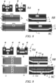
FIG. 6A to 6C schematically represent steps A, B1 and B2; - ∘
FIG. 7A to 7C schematically represent step B3; - ∘
FIG. 8A to 8C schematically represent step C; - ∘
FIG. 9A to 9C schematically represent step D1 and D2; - ∘
FIG. 10A to 10C schematically represent step D3; - ∘
FIG. 11A to 11C schematically represent steps E and F; - ∘
FIG. 12A to 12C schematically represent step G; - ∘
FIG. 13A to 13C schematically represent steps H1 and H2; - ∘
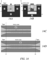
FIG. 14A to 14C schematically represent step I; - ∘
FIG. 15A to 15C schematically represent step I'; - ∘
FIG. 16A to 16C schematically represent step I"; - ∘
FIG. 1 to 4 (above) schematically represent step J;
- ∘
-
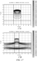
FIG. 17 show two ALCOR software simulations using a beam propagation method, based on a device according to the prior art with a slab structure having a width β from 3 µm to 1,5 µm, with a step of 0,5 µm; -
FIG. 18 show one ALCOR software simulation using a beam propagation method, based on a device according to the prior art with a deeper slab having a width β of 1,5 µm; -
FIG. 19 show one ALCOR software simulation using a beam propagation method, based on a device according to the prior art with a shallower slab structure with a width β of 1,5 µm ; -
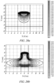
FIG. 20 show 4 ALCOR software simulations using a beam propagation method, based on a device according to the invention. - For each one of
figures 6 to 16 , the reference A corresponds to cross-sectional views perpendicular to the XX' axis, one in the active zone (right-hand schema) and the other in a taper zone (first and/or second taper zones), while references B and C correspond respectively to the first embodiment (with a single taper zone) and the second embodiment (with two taper zones), each of views B and C comprising a top view and a cross-sectional view (except figures only comprising top views). - The same reference number represents the same element or the same type of element on all drawings, unless stated otherwise.
- The figures and the following description illustrate specific exemplary embodiments of the invention. It will thus be appreciated that those skilled in the art will be able to devise various arrangements that, although not explicitly described or shown herein, embody the principles of the invention and are included within the scope of the invention. Furthermore, any examples described herein are intended to aid in understanding the principles of the invention and are to be construed as being without limitation to such specifically recited examples and conditions. As a result, the invention is not limited to the specific embodiments or examples described below, but by the claims and their equivalents.
- In the following description, well-known functions or constructions by the man skilled in the art are not described in detail since they might obscure the invention in unnecessary detail.
- In the following description of the figures, schematic representations are non-limiting and serve only for the understanding of the invention.
-
FIGs. 1A and 1B together with the cross-sectional views ofFIG. 3 schematically represent a first specific embodiment of a Semiconductor optical device D according to the present invention that overcomes the above-mentioned drawbacks. This first specific embodiment of a Semiconductor optical device D comprises: - a substrate 1 (see
FIG. 1A andFIG. 4 ) of n-doped III-V semiconductor material (for instance n-InP) with a longitudinal axis XX' and presenting a base 10 with a planarbottom surface 100 and an upper surface 101 (seeFIG. 1A andFIG. 4 ) andside walls 11, 12 (seeFIG. 4 ) perpendicular to thebase 10, thesubstrate 1 including a central longitudinal cavity C of U-shaped cross-section, whose width α and height δ from the planarbottom surface 100 vary along said longitudinal axis XX'), so as to define at least 2 zones along said longitudinal axis XX' delimited by a first junction J1: a first active zone I and a first taper zone II; - within a first active zone I (see
FIG. 1A ), thebottom surface 100 and theupper surface 101 of the base 10 are parallel to each other and spaced from each other by a constant height δ=δ1, and the central longitudinal cavity C presents a constant width α = α1; - within a second zone II (see
FIG. 1A ) constituting a first taper zone II, wherein theupper surface 101 describes a continuous curved or planar surface comprising twoopposite ends FIG. 3 ) perpendicular to the longitudinal axis XX', one of theends 101A being located at a height d1 at the first junction J1, with δ1 being smaller than the height δ0 at the free end of the first taper zone II, the width α varying from α1 at the first junction J1 to α0 at the free end of the first taper zone II; - a layer of n-doped III-
V semi-conductor material 2 positioned on the upper surface 101 (seeFIG. 1A andFIG. 4 ) of thebase 10 inside the cavity C (seeFIG. 4 ), - a layer of n-inactive III-V
optical waveguide material 3 positioned on the layer of n-doped III-V semi-conductor material 2 inside said cavity C (seeFIG. 1A ), this layer of n-inactive III-Voptical waveguide material 3 having an inverted T shape in a cross-section perpendicular to the longitudinal axis XX' (seeFIG. 3 ), so as to form a slab 3with a bottom 31 of thickness ε and an edge (32) of thickness γ (seeFIGs. 3B to 3D ), with ε being constant and equal to ε1 within the first active zone I (FIGs. 3D ,1A and2A ) and varying within the first taper zone II from ε1 at the first junction J1 to 0 at the free end of the first taper zone II, and with γ being constant and equal to γ1 in the first active zone I and varying within the first taper zone II from γ1 at the first junction J1 to 0 at the free end of the first taper zone II; - a central ribbon R having a width b and comprising, on the
edge 32 of theslab 3, a buried optical waveguide 4 (for instance based on AlGaInAs or GaInAsP MQW) beneath a layer of p-doped III-V semi-conductor 5 such as p-InP (seeFIGs. 3B to 3D and 4 ), - a pair of channels C1, C2 (
FIGs 1B ,3A-3D and4 ) into the n-inactive III-Voptical waveguide 3 along the longitudinal axis (XX) and being located on both sides of the central ribbon R, said longitudinal channels C1, C2 being each filled by a semi-insulating stack or an insulatingstack 6 such as a Semi-Insulating Buried Heterostructure (SIBH) realized in one-step with Fe-InP or Ru-InP.. -
FIG. 1B notably shows that the channels C1, C2 are longitudinal and parallel to each other and of constant width W1 within the first active zone I, but the channels may present each the shape of a trapeze with a width increasing within the first taper zone from W1 at the first junction to WO at the free end of the first taper zone II. -
FIG. 1B also shows that, within the first active zone I,metal stripes sidewall - The specific embodiment shown in
FIGs 1A and 1B is a device working in reflection. It comprises: - an
anti-reflective coating R min 10 positioned at the free end of the first taper zone II, and - a
reflective coating R max 11 positioned at the end of the first active zone I that is opposite to the first junction J1 between said first active zone I and the first taper zone II, -
FIGs. 2A and 2B schematically represent a second specific embodiment of a Semiconductor optical device D according to the present invention that overcomes the above-mentioned drawbacks.FIGs 2A and 2B differs fromFIGs 1A and 1B , respectively in that it is a device working in transmission (and not in reflection). - In particular, this second specific embodiment comprises:
- in the same manner as in the first embodiment, an
anti-reflective coating R min 10 positioned at the free end of the first taper zone II, and - a second taper zone III at the end of the first active zone I that is opposite to the first junction J1, thus defining a second junction J2 between the second taper zone and the first active zone I, and
- another
anti-reflective coating R min 10 positioned at the free end of the second taper zone III, -
FIG. 3 comprises four cross-sectional views of each of the embodiments shown inFIGs. 1 and2 being taken along the taper (see 3A, 3B and 3C) and the first active zones (see 3D): -
FIG. 3A is a cross-sectional of both embodiments according to the A-A' (at the free end of the first taper zone II); -
FIG. 3B is a cross-sectional of both embodiments according to the B-B' (within the first taper zone II); -
FIG. 3C is a cross-sectional of both embodiments according to the A-A' (at the first junction J1); -
FIG. 3D is a cross-sectional of both embodiments according to the D-D' (within the first active zone I). -
FIG. 3 clearly shows the evolution of the slab 3 (made of n-inactive III-V optical waveguide material) along the taper zone II (FIGs. 3A-3C ) and the first active zone (FIG. 3D ). - In the active zone I, the
slab 3 comprises a bottom 31 of thickness ε and anedge 32 of thickness γ.FIG. 3D shows that, within the first active zone I, ε is constant and equal to ε1 and γ is constant and equal to γ1. -
FIGs. 3A to 3C show that, along the taper zone II, ε varies from ε1 at the first junction J1 to 0 at the free end of the taper zone II, and γ varies from γ1 at the first junction J1 to 0 at the free end of the taper zone II. -
FIG. 3 also shows that, on theedge 32 ofslab 3, there is a buried optical waveguide 4 (for instance based on AlGaInAs or GaInAsP MQW) beneath a layer of p-doped III-V semi-conductor 5 such as p-InP.FIG. 3 also clearly show a pair of channels C1, C2 into the n-inactive III-Voptical waveguide 3 along the longitudinal axis (XX) and being located on both sides of the central ribbon R, said longitudinal channels C1, C2 being each filled by a semi-insulating stack or an insulatingstack 6 such as a Semi-Insulating Buried Heterostructure (SIBH) realized in one-step with Fe-InP or Ru-InP. - There are four factors to optimize the device for the most adiabatic transition:
- The bottom width α of the cavity C,
- The width of the ribbon β,
- The thickness γ of the edge of the slab,
- The thickness ε of the bottom of the slab.
- wherein the width α1 of the central longitudinal cavity (C)is constant within the first active zone (I).
- The bottom width α of
SOA slab 3 is as large as possible as long as theoptical guide 4 stays single mode. Before the taper zone II, the width of theoptical guide 4 formed on the upper part of theedge 32 of slab 3decreases as small as possible as long as the optical mode stays in the active zone I. For example (3D), the central part of theoptical guide 4 such as SOAhas a 4 µm width and a 2 µm at the junction J1 between theSOA 1 and the taper zone II (FIG. 3B ). The width of taper zone II is equal to the width of the active zone I at the junction J1 and decreases. For example, the taper zone II has a 2µm width at the junction J1 (butt-joint) and 0.1µm width at the end of the taper zone. The function of this taper zone II is to deconfine the optical mode to facilitate the optical coupling between the component and another component or an optical fiber. -
FIG. 4 shows an additional sectional view (corresponding to the cross-sectional view 4A) of both embodiments of the Semiconductor optical device D according to the A-A' plane, being flip-chipped on an electronic package. - In
FIGs 1 to 4 , the first active zone I comprises one optical function, for instance a Semiconductor optical amplifier or an Electro absorption Modulator (usually known by the acronym EAM). - In
FIGs 5A to 5D , the Semiconductor optical device D corresponds to the first specific embodiment shown inFIG. 1A and 1B working in reflection, with the first active zone I respectfully comprising: - In
FIG. 5A , one optical function comprising a Distributed Feed-Back Laser (i.e. a Distributed Feedback Grating (or DFB grating) is etched inside the layer of p-doped III-V semi-conductor material 5); - In
FIG. 5B , two optical functions comprisinga SOA and a EAM, the Semiconductor optical device D being thus a reflective electro-absorption modulator monolithically integrated with semiconductor optical amplifier (REAMSOA) (hereinafter referred to as the acronym REAMSOA); - In
FIG. 5C , two optical functions comprisingan EAM or a SOA and a Distributed Feed-Back Laser (with a DFB grating being etched inside the layer of p-doped III-V semi-conductor material 5), the Semiconductor optical device D constituting thus either an electro-absorption modulated laser (hereinafter referred to as the acronym EML and comprising a DFB laser and a EAM) or a Master Oscillator Power Amplifier (hereinafter referred to as the acronym MOPA and comprising a DFB laser and a SOA); - In
FIG. 5D , three optical functions comprisinga SOA, an EAM and a Distributed Feed-Back Laser (with a DFB grating being etched inside the layer of p-doped III-V semi-conductor material 5), the Semiconductor optical device D constituting an amplified EML (comprising a DFB laser, an EAM and a SOA). -
FIGs. 6 to 16 (together with the above-describedFIGs. 1 to 4 ) schematically represent the different steps of the process flow for fabricating a semiconductor optical device (D) according to the embodiments earlier described. - In particular,
FIG. 6 schematically represents A, B1 and B2 being composed in detail of: - A) providing substrate material 1' made of n-doped III-V semiconductor material (for instance n-InP) with a longitudinal axis XX' (see
FIGs. 5A and 5B ), and presenting abottom surface 100 and atop surface 110; - B1) depositing a first dielectric layer M1 (for instance based on based on SiO2 or Si3N4) on said
top surface 110; - B2) patterning the first dielectric layer M1 (for instance base on SiO2 or Si3N4) so as to define at least 2 zones along said longitudinal axis XX including a first zone intended to constitute the first active zone I, a second zone II (see
FIGs 6B and 6C ) and if applicable a third zone III (onlyFIG. 6C ), the first active zone I and the first taper zone II being delimited by a first junction J1 (notably a butt-joint) and the first active zone I and the second taper zone III being delimited by a second junction J2 (notably a butt-joint). - The sub-step B2 of patterning the first dielectric layer M1 may comprise the sub-steps of:
- applying a layer of positive photoresin on the top surface of the first dielectric layer M1
- applying a gray lithographic mask to said layer of positive photoresin, the gray lithographic mask comprising a transparent area corresponding to the central rectangle-shaped portion in the first active zone I and an area corresponding to the central trapezoidal portion in the taper zone II, III, the opacity progressing along the taper zones II, III from full transparency at the junction J1, J2 to full opacity at the ends of the taper zones II opposite to said junctions J1, J2 ;
- Then,
FIG. 7 represents step B3 consisting in an irradiation of the positive photoresin and the lithography mask, the resin development and an etching by Reactive Ion Etching, so as to form asubstrate 1 having a base 10 with a planarbottom surface 100 and anupper surface 101,side walls base 10, and a central longitudinal cavity C of U-shaped cross-section, the height δ of theupper surface 101 from the planarbottom surface 100 being constant and equal to δ1 along the first active zone I and varying from δ1 at the junctions J1, J2 to δ 0 at the free end of the taper zones II, III), with δ 0 greater than δ 1. - Then,
FIG. 8 represents step C composed in detail of: - performing an epitaxial growth of a layer of n-doped III-
V semi-conductor 2, and - performing an epitaxial growth of a layer of n-inactive III-
V material stack 3 of thickness h to fill the cavity C; - Then,
FIG. 9 represents steps D1 and D2 composed in detail of: - D1) depositing on said layer of n-inactive III-V material stack 3 a second dielectric layer M2 (for instance made of based on SiO2 or Si3N4) of thickness D;
- D2) patterning and etching the second dielectric layer M2 along the longitudinal axis XX' so that the second dielectric layer M2 is not etched at all along the first active zone I and partially etched along the taper zones II, III, the thickness D of this second dielectric layer decreasing from D at the junctions J1, J2 to 0 at the ends of the taper zones II, III opposite to the junctions J1, J2.
- The sub-step D2 of patterning the second dielectric layer M may comprise the sub-steps of:
- applying a layer of positive photoresin on the n-inactive III-
V material stack 3 inside the cavity C; - applying a gray lithographic mask to said layer of positive photoresin, said gray lithographic mask comprising an opaque area corresponding to the form of the cavity C in the first active zone I and an area corresponding to the form of the cavity C in the taper zones II, III, the opacity of which progresses along the first taper zone II from full opacity at the junctions J1, J2 to full transparency at the end of the taper zones II, III opposite to the junctions J1, J2.
-
FIG. 10A to 10C schematically represent step D3 consisting in an irradiation of the positive photoresin and the lithography mask, the resin development and an etching by Reactive Ion Etching, so as to define a slope from the free end of each taper zone II, III down to the respective junctions J1, J2, with the height h of layer 3varying along the taper zones II, III, from each junction J1, J2 down to 0 at the free end of the taper zones II, III. The n-inactive III-V material stack 3 is totally etched at the output of the taper zones II, III.. - The second dielectric layer M2 is removed.
-
FIG. 11A to 11C schematically represent steps E and F comprising: - performing, on the layer of n-inactive III-
V material stack 3 inside the cavity C, an epitaxial growth an active III-V material stack 4 (for instance based on AlGaInAs or GaInAsP MQW) ; - performing, on said active III-
V material stack 4 inside the cavity C, an epitaxial growth of a layer of p-doped III-V semi-conductor 5 up to at least the level of the top of theside walls - Then, the remaining portions of the first dielectric layer M1 are removed, as shown by
FIGs. 12A to 12C (step G). - Then, the next step comprises a selectively etching, into the n-inactive III-V
optical waveguide 3 and along the longitudinal axis XX', a pair of channels C1, C2, each located along eachside wall - the layer of n-inactive III-V
optical waveguide 3 having an inverted T shape in a cross-section perpendicular to the longitudinal axis (XX'), so as to form aslab 3 with a bottom 31 of thickness ε and anedge 32 of thickness γ, with ε being constant and equal to ε1 within the first active zone I and varying within the first taper zone II from ε1 at the first junction J1 to 0 at the free end of zone II, with γ being constant and equal to γ1 in the first active zone I and varying within the first taper zone II from γ1 at the first junction J1 to 0 at the free end of the first taper zone II; - the etched
active material stack 4 constituting an active optical guide, and - the etched layer of p-doped III-
V semi-conductor material 5. - This selective etching step D is realized as follows:
-
FIG. 13A to 13C show that step H further comprises sub-steps H1 and H2 comprising: - H1- depositing, on the top of the
side walls - H2- patterning and etching said third dielectric layer M3 along the longitudinal axis XX' so that the third dielectric layer M3 is s not etched at all along the first active zone I and partially etched along the taper zones II, III, the thickness E decreasing from the junctions J1, J2 to the ends of the taper zone II, III opposite to the junctions J1, J2.
- The sub-step H2 of patterning third dielectric layer (M3) may comprise the sub-steps of:
- applying a layer of positive photoresin on the top of the
side walls - applying a gray lithographic mask to said layer of positive photoresin, said gray lithographic mask having the form of the channels C1, C2 and being opaque along the first active zone I and less opaque along the taper zones II, III, the opacity of which progresses along the taper zones II, III from full opacity at the junction J1 to less opacity at the end of the taper zones II, III which is opposite to the junctions J1, J2;
- irradiating the positive photoresin and the lithography mask by Reactive Ion Etching.
-
FIG. 14A to 14C schematically represent step I comprising the performing, inside the channels C1, C2, of the regrowth of insulating or asemi-insulating stack 6 up to at least the level of the top of the layer of p-doped III-V semi-conductor material 5. - Then the third dielectric layer M3 is removed (see
FIG. 15 : step I' of removing the remaining portions of the third dielectric layer M3). - The method of fabricating may further comprise between steps I') and J), a step II") of chemical and/or mechanical surface stripping of the regrown insulating or semi-insulating stack, to flatten it to the level of the top of the side walls (see
FIG. 16 ). -
FIGs. 17 to 19 show different ALCOR software simulations using a beam propagation method, based on a device according to the prior art. Usually, a taper in Semiconductor optical devices is a simple shrinkage of the active layer. However, in a case of a slab structure, it is less evident. All the ALCOR software simulations ofFIGs. 17 to 19 show that: - the optical guide keeps the single mode performances by decreasing the width of the active layer (
Fig 17A ). - If the width of the decreases the optical mode leaves the active layer where is the amplification to the slab layer. The optical mode becomes less circular and flatter and more extended, which is a drawback for the coupling (
FIG. 17 ). - in case of a deeper slab, the optical guide becomes multimode, which is a drawback because the optical power will spread out over the different optical modes. There will be an optical performance loss (
Fig 18 ). - in case a shallower slab, the optical mode leaves the active layer where is the amplification to the slab layer. The optical mode becomes less circular and flatter and more extended than previously, which is still a drawback for the coupling (
Fig 19 ). -
FIG. 20 show 4 ALCOR software simulations using a beam propagation method, based on a device according to the invention - In
fIG. 20a , the optical mode is located in the larger part of the active zone I (width β of 4pm). The slab design permits to increase the width β to increase the gain in the active section I. - When the width of the ribbon decreases (down to 2 µm) to reach the entrance of the taper, the optical mode is located in the MQW layers of the optical waveguide but overlaps the slab layer (
Figure 20 b) . - By decreasing further the width of the
slab 3 and by decreasing the width of the ribbon (down to 1,5 µm), it is possible to keep the a single optical mode and to increase the confinement of the optical mode in the MQW layers of theoptical waveguide 4 and to decrease the confinement of the optical mode in the slab layer (FIG. 20c et FIG. 20d ): - For a width of 1,5 µm, the optical mode is located at the entrance of the taper zone II (
FIG. 20 c) , - For a width of 1 µm the optical mode is located in the taper zone II (
FIG. 20 d) . - By decreasing further the width of the slab layer and by decreasing the width of the ribbon (down to 0,5 µm), the optical mode is located at the output of the taper zone II. The modelisation shown in
FIG. 20 is computed by considering that the thickness of the slab layer varies linearly with the width of the ribbon β.
Claims (16)
- Semiconductor optical device (D) comprising:- a substrate (1) of n-doped III-V semiconductor material with a longitudinal axis (XX') and presenting a base (10) with a planar bottom surface (100) and an upper surface (101) and side walls (11, 12) that are perpendicular to said base (10),o said substrate (1) including a central longitudinal cavity (C) of U-shaped cross-section, whose width α and height δ from the planar bottom surface (100) vary along said longitudinal axis (XX'), so as to define at least 2 zones along said longitudinal axis (XX') delimited by a first junction (J1):▪ a first active zone (I), wherein the bottom surface (100) and the upper surface (101) of the base (10) are parallel to each other and spaced from each other by a constant height δ = δ1, and the central longitudinal cavity (C) presents a constant width α = α1,▪ a second zone (II) constituting a first taper zone (II), wherein the upper surface (101) describes a continuous curved or planar surface comprising two opposite ends (101A, 101B) perpendicular to the longitudinal axis (XX'), one of the ends (101A), being located at a height δ1 at the first junction (J1) which is lower than the height δ 0 at the free end of the first taper zone (II), the width α varying from α1 at the first junction (J1) to α0 at the free end of the first taper zone (II),- a layer of n-doped III-V semi-conductor material (2) positioned on the upper surface (101) of the base (10) inside the cavity (C),;- a layer of n-inactive III-V optical waveguide material (3) positioned on the layer of n-doped III-V semi-conductor material (2) inside said cavity (C), said layer of n-inactive III-V optical waveguide material (3) having an inverted T shape in a cross-section perpendicular to the longitudinal axis (XX'), so as to form a slab with a bottom (31) of thickness ε and an edge (32) of thickness γ, with ε being constant and equal to ε 1 within the first active zone (I) and varying within the first taper zone (II) from ε1 at the first junction (J1) to 0 at the free end of the first taper zone (II), and with γ being constant and equal to γ 1 in the first active zone (I) and varying within the first taper zone (II) from γ 1 at the first junction (J1) to 0 at the free end of the first taper zone (II);- said semiconductor optical device (D) further comprising:o a central ribbon (R) having a width β and comprising, on the edge (32) of the slab, a buried optical waveguide (4) beneath a layer of p-doped III-V semi-conductor (5),o a pair of channels (C1, C2) into the n-inactive III-V optical waveguide (3) along the longitudinal axis (XX) and being located on both sides of the central ribbon (R), said longitudinal channels (C1, C2) being each filled by a semi-insulating stack or an insulating stack (6), said channels (C1, C2) being longitudinal and parallel to each other and of constant width W1 within the first active zone (I),o within the first active zone (I), metal stripes (71, 73) covering the top of each sidewall (11,12) and a metal stripe covering the top of the layer of p-doped III-V semi-conductor (5) .
- Semiconductor optical amplifier device (D) according to claim 1, further comprising:- an anti-reflective coating Rmin (10) positioned at the free end of the first taper zone (II), and- a reflective coating Rmax (11) positioned at the end of the SOA zone (I) that is opposite to the first junction (J1) between said SOA zone (I) and said first taper zone (II),so that the anti-reflective coating Rmin (10) constitutes the entrance and the output of said semiconductor optical amplifier device (D) working in reflexion.
- Semiconductor optical amplifier device (D) according to claim 1, further comprising:- a second taper zone (III) at the end of the SOA zone (I) that is opposite to the first junction (J1), thus defining a second junction (J2) between the second tape zone (III) and the SOA zone (I),- another anti-reflective coating Rmin (10) positioned at the free ends of the first taper zone (II) and second taper zone (III),so that one of the anti-reflective coatings Rmin (10) constitutes the entrance of said semiconductor optical amplifier device (D) and the other anti-reflective coatings Rmin (10) constitutes the output of said semiconductor optical amplifier device (D) working in transmission.
- Semiconductor optical device (D) according to anyone of claims 1 to 3, wherein the width α1 of the central longitudinal cavity (C) within the first active zone (I) is constant.
- Semiconductor optical device (D) according to anyone of claims 1 to 3, wherein, within the first taper zone (II), the width α of the central longitudinal cavity (C) increases from α1 at the first junction (J1) and, if applicable, at the second junction (J2) to α0 at the free end of the first taper zone (II).
- Semiconductor optical device (D) according to anyone of claims 1 to 5, wherein a width β of the central ribbon (R) within the first active zone (I) continuously varies from 1,5 µm at the first junction (J1) and to 15 µm in the middle of the first active zone (I), and the width β of the central ribbon (R) within the first taper zone (II) varies from 1,5 µm at the first junction (J1) to 0,1 µm at the free ends of the first taper zone (II) and, if applicable, of the second taper zone (III).
- Semiconductor optical device (D) according to anyone of claims 1 to 6, wherein the upper surface (101) of the base (10) is planar and defines a slope from one of the free end of the first (II) down to the first junction (J1), said slope having a height difference δ0 - δ1 of 0,05 µm.
- Semiconductor optical device (D) according to anyone of claims 1 to 7, wherein the slab presents a global height h= ε + γ varying:- within the first active zone (I), from 1 µm at the first junction (J1) to 10 µm in the middle of the first active zone (I),- within the first (II), from 1 µm at the first junction (J1), at the second junction (J2) to 0 at the free end of the first taper zone (II).
- Semiconductor optical device (D) according to anyone of claims 1 to 8, wherein the length of the first taper zone (II), varies from 20 µm to 200 µm, with a global height h=ε + γ at the junction (J1) and, if applicable, at the second junction (J2), varying from 1 µm to 10 µm.
- Semiconductor optical device (D) according to anyone of claims 1 to 9, wherein the first active zone (I) comprises a Semiconductor optical amplifier, or a laser, or a modulator, or a laser modulator, or a laser Semiconductor Optical Amplifier, or a laser modulator Semiconductor Optical Amplifier.
- Method of fabricating a semiconductor optical device (D) comprising:A) providing a substrate material (1') made of n-doped III-V semiconductor material with a longitudinal axis (XX), and presenting a bottom surface (100) and a top surface (110);B) etching said substrate material (1') so as to form a substrate (1) having a base (10) with a planar bottom surface (100) and an upper surface (101), side walls (11, 12) perpendicular to said base (10), and a central longitudinal cavity (C) of U-shaped cross-section, the height δ of the upper surface (101) from the planar bottom surface (100) being constant and equal to δ1 along the first active zone (I) and varying from δ1 at the junction (J1) to δ0 at the free end of the first taper zone (II), with δ 0 greater than δ 1 ;C) performing an epitaxial growth of a layer of n-doped III-V semi-conductor (2) and a layer of n-inactive III-V material stack (3) of thickness h to fill the cavity (C);D) selectively etching the layer of n-inactive III-V material stack (3) so that it defines a slope from the free end of the first taper zones (II) down to the first junction (J1), with the height h varying along the first taper zone (II), from the first junction (J1) down to 0 at the free end of the first taper zone (II);E) performing, on the layer of n-inactive III-V material stack (3) inside the cavity (C), an epitaxial growth an active III-V material stack (4);F) performing, on said active III-V material stack (4) inside the cavity (C), an epitaxial growth of a layer of p-doped III-V semi-conductor (5) up to at least the level of the top of the side walls (11, 22);G) removing the remaining portions of the first dielectric layer (M1);H) selectively etching, into the n-inactive III-V optical waveguide (3) and along the longitudinal axis (XX), a pair of channels (C1, C2), each located along each side wall (21, 22) so as to define a central ribbon (R) comprising:- the layer of n-inactive III-V optical waveguide (3) having an inverted T shape in a cross-section perpendicular to the longitudinal axis (XX'), so as to form a slab with a bottom (31) of thickness ε and an edge (32) of thickness γ, with ε being constant and equal to ε1 within the first active zone (I) and varying within the first taper zone (II) from ε1 at the first junction (J1) to 0 at the free end of zone (II), with γ being constant and equal to yl in the first active zone (I) and varying within the first taper zone (II) from γ1 at the first junction (J1) to 0 at the free end of the first taper zone (II);- the etched active material stack (4) constituting an active optical guide, and- the etched layer of p-doped III-V semi-conductor material (5);I) inside the channels (C1, C2), performing regrowth of an insulating or semi-insulating stack (6) up to at least the level of the top of the layer of p-doped III-V semi-conductor material (5);J) depositing, along said longitudinal axis (XX), metal stripes (71, 72, 73) on the top of the side walls (11, 12) and on the top of the central ribbon (R).
- Method according to claim 11, wherein step B comprises the sub-steps of:B1 -depositing a first dielectric layer (M1) on said top surface (110);B2 -patterning said first dielectric layer (M1) so as to define at least 2 zones along said longitudinal axis (XX) including a first zone intended to constitute the first active zone (I) and a second zone (II) intended to constitute the first taper zone (II), said first active zone (I) and said first taper zone (II) being delimited by a first junction (J1),B3 -etching said first dielectric layer (M1) so that it is entirely etched along the first active zone (I) in a central rectangle-shaped portion of width α1 and partially etched along the first taper zone (II) in a central trapezoidal portion of width α varying from α 1 at the junction (J1) to α 0 at the end of the first taper zone (II) that is opposite to said junction (J1).
- Method according to claim 10, wherein step D of selectively etching the layer of n-inactive III-V material stack (3) comprises the sub-steps of:D1- depositing on said layer of n-inactive III-V material stack (3) a second dielectric layer (M2) of thickness D;D2- patterning and etching said dielectric layer (M2) along said longitudinal axis (XX) so that said dielectric layer (M2) is s not etched at all along the first active zone (I) and partially etched along the first taper zone (II), the thickness D decreasing from D at the first junction (J1) to 0 at the end of the first taper zone (II) that is opposite to said junction (J1);D3- removing said second dielectric layer (M2).
- Method according to anyone of claims 12 and 13, wherein the sub-steps B2 or D2 of patterning the first and second dielectric layers (M1, M2) comprises the sub-steps of:- applying a layer of positive photoresin on the top surface (110) of the first or second dielectric layers (M1, M2);- applying a gray lithographic mask to said layer of positive photoresin, said gray lithographic mask comprising:• in the case of subs-step B2, a transparent area corresponding to the central rectangle-shaped portion in the first active zone (I) and an area corresponding to the central trapezoidal portion in the first taper zone (II) and the opacity of which progresses along the first taper zone (II) from full transparency at the junction (J1) to full opacity at the end of the first taper area (II) which is opposite to said junction (J1);• in the case of sub-step D2, an opaque area corresponding to the form of the cavity (C) in the first active zone (I) and an area corresponding to the form of the cavity (C) in the first taper zone (II), the opacity of which progresses along the first taper zone (II) from full opacity at the junction (J1) to full transparency at the end of the first taper zone (II) which is opposite to said junction (J1),andwherein steps B3 or D3 comprise an irradiation of the positive photoresin and the lithography mask by Reactive Ion Etching.
- Method according to anyone of claims 11 to 14, wherein step H of selectively etching, into the n-inactive III-V optical waveguide (3) and along the longitudinal axis (XX'), a pair of channels (C1, C2), is realized in a similar manner as sub-step D2 and comprises the sub-steps of:H1- depositing, on the top of the side walls (11, 12) and the top of the central ribbon (R), a third dielectric layer (M3) of thickness E;H2- patterning and etching said third dielectric layer (M3) along said longitudinal axis (XX') so that said third dielectric layer (M3) is not etched at all along the first active zone (I) and partially etched along the first taper zone (II), the thickness E decreasing from the first junction (J1) to the end of the first taper zone (II) that is opposite to said first junction (J1).
- Method according to claim 15, wherein step the sub-step H2 of patterning third dielectric layer (M3) comprises the sub-steps of:- applying a layer of positive photoresin on the top of the side walls (11, 12) and the top of the central ribbon (R);- applying a gray lithographic mask to said layer of positive photoresin, said gray lithographic mask having the form of the channels (C1, C2) and being opaque along the first active zone (I) and less opaque along the first taper zone (II), the opacity of which progresses along the first taper area (II) from full opacity at the junction (J1) to less opacity at the end of the first taper zone (II) which is opposite to said junction (J1);- irradiating the positive photoresin and the lithography mask by Reactive Ion Etching.
Priority Applications (2)
| Application Number | Priority Date | Filing Date | Title |
|---|---|---|---|
| EP22306085.6A EP4311042B1 (en) | 2022-07-21 | 2022-07-21 | Opto-electronic device |
| US18/335,584 US20240039250A1 (en) | 2022-07-21 | 2023-06-15 | Opto-electronic device |
Applications Claiming Priority (1)
| Application Number | Priority Date | Filing Date | Title |
|---|---|---|---|
| EP22306085.6A EP4311042B1 (en) | 2022-07-21 | 2022-07-21 | Opto-electronic device |
Publications (2)
| Publication Number | Publication Date |
|---|---|
| EP4311042A1 true EP4311042A1 (en) | 2024-01-24 |
| EP4311042B1 EP4311042B1 (en) | 2025-10-15 |
Family
ID=82846176
Family Applications (1)
| Application Number | Title | Priority Date | Filing Date |
|---|---|---|---|
| EP22306085.6A Active EP4311042B1 (en) | 2022-07-21 | 2022-07-21 | Opto-electronic device |
Country Status (2)
| Country | Link |
|---|---|
| US (1) | US20240039250A1 (en) |
| EP (1) | EP4311042B1 (en) |
Cited By (1)
| Publication number | Priority date | Publication date | Assignee | Title |
|---|---|---|---|---|
| WO2025215186A1 (en) * | 2024-04-12 | 2025-10-16 | SMART Photonics Holding B.V. | Photonic-integrated soa for varying mode profile to combine high gain and high power |
Citations (7)
| Publication number | Priority date | Publication date | Assignee | Title |
|---|---|---|---|---|
| US4321556A (en) * | 1979-01-18 | 1982-03-23 | Nippon Electric Co., Ltd. | Semiconductor laser |
| EP0641049A1 (en) * | 1993-08-31 | 1995-03-01 | Fujitsu Limited | An optical semiconductor device and a method of manufacturing the same |
| JPH08264748A (en) * | 1995-03-27 | 1996-10-11 | Furukawa Electric Co Ltd:The | Optical waveguide integrated circuit device and manufacturing method thereof |
| US20010053260A1 (en) * | 2000-03-13 | 2001-12-20 | Toshiyuki Takizawa | Optical module and method for producing the same, and optical circuit device |
| US20040125846A1 (en) * | 2000-04-11 | 2004-07-01 | Nuvonyx, Inc. | Tailored index single mode optical amplifiers and devices and systems including same |
| US20190260182A1 (en) * | 2018-02-16 | 2019-08-22 | Kyocera Corporation | Semiconductor module and manufacturing method thereof |
| US20220173573A1 (en) * | 2019-06-19 | 2022-06-02 | Mitsubishi Electric Corporation | Semiconductor optical element |
Family Cites Families (1)
| Publication number | Priority date | Publication date | Assignee | Title |
|---|---|---|---|---|
| GB2589092B (en) * | 2019-11-15 | 2022-02-16 | Rockley Photonics Ltd | III-V / Silicon optoelectronic device and method of manufacture thereof |
-
2022
- 2022-07-21 EP EP22306085.6A patent/EP4311042B1/en active Active
-
2023
- 2023-06-15 US US18/335,584 patent/US20240039250A1/en active Pending
Patent Citations (7)
| Publication number | Priority date | Publication date | Assignee | Title |
|---|---|---|---|---|
| US4321556A (en) * | 1979-01-18 | 1982-03-23 | Nippon Electric Co., Ltd. | Semiconductor laser |
| EP0641049A1 (en) * | 1993-08-31 | 1995-03-01 | Fujitsu Limited | An optical semiconductor device and a method of manufacturing the same |
| JPH08264748A (en) * | 1995-03-27 | 1996-10-11 | Furukawa Electric Co Ltd:The | Optical waveguide integrated circuit device and manufacturing method thereof |
| US20010053260A1 (en) * | 2000-03-13 | 2001-12-20 | Toshiyuki Takizawa | Optical module and method for producing the same, and optical circuit device |
| US20040125846A1 (en) * | 2000-04-11 | 2004-07-01 | Nuvonyx, Inc. | Tailored index single mode optical amplifiers and devices and systems including same |
| US20190260182A1 (en) * | 2018-02-16 | 2019-08-22 | Kyocera Corporation | Semiconductor module and manufacturing method thereof |
| US20220173573A1 (en) * | 2019-06-19 | 2022-06-02 | Mitsubishi Electric Corporation | Semiconductor optical element |
Cited By (1)
| Publication number | Priority date | Publication date | Assignee | Title |
|---|---|---|---|---|
| WO2025215186A1 (en) * | 2024-04-12 | 2025-10-16 | SMART Photonics Holding B.V. | Photonic-integrated soa for varying mode profile to combine high gain and high power |
Also Published As
| Publication number | Publication date |
|---|---|
| EP4311042B1 (en) | 2025-10-15 |
| US20240039250A1 (en) | 2024-02-01 |
Similar Documents
| Publication | Publication Date | Title |
|---|---|---|
| US10534131B2 (en) | Semiconductor optical integrated device having buried hetero structure waveguide and deep ridge waveguide | |
| US5805755A (en) | Self-aligned transition from ridge to buried heterostructure waveguide, especially for multi-wavelength laser array integration | |
| US8965153B2 (en) | Optical semiconductor device and optical waveguide | |
| US7796656B2 (en) | Enhanced efficiency laterally-coupled distributed feedback laser | |
| US8363314B2 (en) | Reflective semiconductor optical amplifier (R-SOA) and superluminescent diode (SLD) | |
| EP0641049B1 (en) | An optical semiconductor device and a method of manufacturing the same | |
| US9423565B2 (en) | Coupled waveguide apparatus and structures therefor | |
| US20020051615A1 (en) | Slab-coupled optical waveguide laser and amplifier | |
| US20100284019A1 (en) | Semiconductor integrated optical device and method of making the same | |
| JPH04243216A (en) | Method for manufacturing optical waveguide, integrated optical device and method for manufacturing the same | |
| JP2008113041A (en) | Waveguide | |
| US12027818B2 (en) | Semiconductor laser | |
| EP4311042B1 (en) | Opto-electronic device | |
| US20030095751A1 (en) | Semiconductor optical devices and methods of making them | |
| EP3970246B1 (en) | Optical device with passive window | |
| CN111937259A (en) | Semiconductor optical device, semiconductor optical integrated device, and method for manufacturing semiconductor optical device | |
| US12586985B2 (en) | Distributed feedback laser with complex coupling | |
| EP0876696B1 (en) | Semiconductor lasers | |
| KR100576299B1 (en) | Semiconductor laser and element for optical communication | |
| CN119518414B (en) | Monolithically integrated laser chip and preparation method and application thereof | |
| JP2605650B2 (en) | Optical isolator | |
| US12259561B2 (en) | Spot-size converter | |
| WO2025037387A1 (en) | Semiconductor laser | |
| JP2000183443A (en) | Semiconductor laser device with spot size converter and method of manufacturing the same | |
| JP2000357789A (en) | Optical integrated device and manufacturing method thereof |
Legal Events
| Date | Code | Title | Description |
|---|---|---|---|
| PUAI | Public reference made under article 153(3) epc to a published international application that has entered the european phase |
Free format text: ORIGINAL CODE: 0009012 |
|
| STAA | Information on the status of an ep patent application or granted ep patent |
Free format text: STATUS: THE APPLICATION HAS BEEN PUBLISHED |
|
| AK | Designated contracting states |
Kind code of ref document: A1 Designated state(s): AL AT BE BG CH CY CZ DE DK EE ES FI FR GB GR HR HU IE IS IT LI LT LU LV MC MK MT NL NO PL PT RO RS SE SI SK SM TR |
|
| STAA | Information on the status of an ep patent application or granted ep patent |
Free format text: STATUS: REQUEST FOR EXAMINATION WAS MADE |
|
| 17P | Request for examination filed |
Effective date: 20240605 |
|
| RBV | Designated contracting states (corrected) |
Designated state(s): AL AT BE BG CH CY CZ DE DK EE ES FI FR GB GR HR HU IE IS IT LI LT LU LV MC MK MT NL NO PL PT RO RS SE SI SK SM TR |
|
| GRAP | Despatch of communication of intention to grant a patent |
Free format text: ORIGINAL CODE: EPIDOSNIGR1 |
|
| STAA | Information on the status of an ep patent application or granted ep patent |
Free format text: STATUS: GRANT OF PATENT IS INTENDED |
|
| INTG | Intention to grant announced |
Effective date: 20250121 |
|
| GRAJ | Information related to disapproval of communication of intention to grant by the applicant or resumption of examination proceedings by the epo deleted |
Free format text: ORIGINAL CODE: EPIDOSDIGR1 |
|
| STAA | Information on the status of an ep patent application or granted ep patent |
Free format text: STATUS: REQUEST FOR EXAMINATION WAS MADE |
|
| GRAP | Despatch of communication of intention to grant a patent |
Free format text: ORIGINAL CODE: EPIDOSNIGR1 |
|
| STAA | Information on the status of an ep patent application or granted ep patent |
Free format text: STATUS: GRANT OF PATENT IS INTENDED |
|
| INTC | Intention to grant announced (deleted) | ||
| RIC1 | Information provided on ipc code assigned before grant |
Ipc: G02F 1/39 20060101ALN20250522BHEP Ipc: G02B 6/12 20060101ALN20250522BHEP Ipc: H01S 5/22 20060101ALN20250522BHEP Ipc: H01S 5/50 20060101ALN20250522BHEP Ipc: H01S 5/042 20060101ALN20250522BHEP Ipc: H01S 5/10 20210101ALI20250522BHEP Ipc: H01S 5/02 20060101AFI20250522BHEP |
|
| INTG | Intention to grant announced |
Effective date: 20250606 |
|
| GRAS | Grant fee paid |
Free format text: ORIGINAL CODE: EPIDOSNIGR3 |
|
| GRAA | (expected) grant |
Free format text: ORIGINAL CODE: 0009210 |
|
| STAA | Information on the status of an ep patent application or granted ep patent |
Free format text: STATUS: THE PATENT HAS BEEN GRANTED |
|
| AK | Designated contracting states |
Kind code of ref document: B1 Designated state(s): AL AT BE BG CH CY CZ DE DK EE ES FI FR GB GR HR HU IE IS IT LI LT LU LV MC MK MT NL NO PL PT RO RS SE SI SK SM TR |
|
| REG | Reference to a national code |
Ref country code: GB Ref legal event code: FG4D Ref country code: CH Ref legal event code: F10 Free format text: ST27 STATUS EVENT CODE: U-0-0-F10-F00 (AS PROVIDED BY THE NATIONAL OFFICE) Effective date: 20251015 |
|
| REG | Reference to a national code |
Ref country code: DE Ref legal event code: R096 Ref document number: 602022023012 Country of ref document: DE |
|
| REG | Reference to a national code |
Ref country code: IE Ref legal event code: FG4D |
|
| REG | Reference to a national code |
Ref country code: NL Ref legal event code: MP Effective date: 20251015 |
|
| REG | Reference to a national code |
Ref country code: AT Ref legal event code: MK05 Ref document number: 1847899 Country of ref document: AT Kind code of ref document: T Effective date: 20251015 |
|
| PG25 | Lapsed in a contracting state [announced via postgrant information from national office to epo] |
Ref country code: NL Free format text: LAPSE BECAUSE OF FAILURE TO SUBMIT A TRANSLATION OF THE DESCRIPTION OR TO PAY THE FEE WITHIN THE PRESCRIBED TIME-LIMIT Effective date: 20251015 |
|
| PG25 | Lapsed in a contracting state [announced via postgrant information from national office to epo] |
Ref country code: ES Free format text: LAPSE BECAUSE OF FAILURE TO SUBMIT A TRANSLATION OF THE DESCRIPTION OR TO PAY THE FEE WITHIN THE PRESCRIBED TIME-LIMIT Effective date: 20251015 |
|
| REG | Reference to a national code |
Ref country code: LT Ref legal event code: MG9D |
|
| PG25 | Lapsed in a contracting state [announced via postgrant information from national office to epo] |
Ref country code: NO Free format text: LAPSE BECAUSE OF FAILURE TO SUBMIT A TRANSLATION OF THE DESCRIPTION OR TO PAY THE FEE WITHIN THE PRESCRIBED TIME-LIMIT Effective date: 20260115 |
|
| PG25 | Lapsed in a contracting state [announced via postgrant information from national office to epo] |
Ref country code: FI Free format text: LAPSE BECAUSE OF FAILURE TO SUBMIT A TRANSLATION OF THE DESCRIPTION OR TO PAY THE FEE WITHIN THE PRESCRIBED TIME-LIMIT Effective date: 20251015 Ref country code: AT Free format text: LAPSE BECAUSE OF FAILURE TO SUBMIT A TRANSLATION OF THE DESCRIPTION OR TO PAY THE FEE WITHIN THE PRESCRIBED TIME-LIMIT Effective date: 20251015 Ref country code: HR Free format text: LAPSE BECAUSE OF FAILURE TO SUBMIT A TRANSLATION OF THE DESCRIPTION OR TO PAY THE FEE WITHIN THE PRESCRIBED TIME-LIMIT Effective date: 20251015 |
|
| PG25 | Lapsed in a contracting state [announced via postgrant information from national office to epo] |
Ref country code: RS Free format text: LAPSE BECAUSE OF FAILURE TO SUBMIT A TRANSLATION OF THE DESCRIPTION OR TO PAY THE FEE WITHIN THE PRESCRIBED TIME-LIMIT Effective date: 20260115 |
|
| PG25 | Lapsed in a contracting state [announced via postgrant information from national office to epo] |
Ref country code: IS Free format text: LAPSE BECAUSE OF FAILURE TO SUBMIT A TRANSLATION OF THE DESCRIPTION OR TO PAY THE FEE WITHIN THE PRESCRIBED TIME-LIMIT Effective date: 20260215 |
|
| PG25 | Lapsed in a contracting state [announced via postgrant information from national office to epo] |
Ref country code: PT Free format text: LAPSE BECAUSE OF FAILURE TO SUBMIT A TRANSLATION OF THE DESCRIPTION OR TO PAY THE FEE WITHIN THE PRESCRIBED TIME-LIMIT Effective date: 20260216 |
|
| PG25 | Lapsed in a contracting state [announced via postgrant information from national office to epo] |
Ref country code: PL Free format text: LAPSE BECAUSE OF FAILURE TO SUBMIT A TRANSLATION OF THE DESCRIPTION OR TO PAY THE FEE WITHIN THE PRESCRIBED TIME-LIMIT Effective date: 20251015 |
|
| PG25 | Lapsed in a contracting state [announced via postgrant information from national office to epo] |
Ref country code: LV Free format text: LAPSE BECAUSE OF FAILURE TO SUBMIT A TRANSLATION OF THE DESCRIPTION OR TO PAY THE FEE WITHIN THE PRESCRIBED TIME-LIMIT Effective date: 20251015 |
|
| PG25 | Lapsed in a contracting state [announced via postgrant information from national office to epo] |
Ref country code: BG Free format text: LAPSE BECAUSE OF FAILURE TO SUBMIT A TRANSLATION OF THE DESCRIPTION OR TO PAY THE FEE WITHIN THE PRESCRIBED TIME-LIMIT Effective date: 20251015 |