EP4311025A2 - Metal plate antenna and antenna device - Google Patents
Metal plate antenna and antenna device Download PDFInfo
- Publication number
- EP4311025A2 EP4311025A2 EP23177503.2A EP23177503A EP4311025A2 EP 4311025 A2 EP4311025 A2 EP 4311025A2 EP 23177503 A EP23177503 A EP 23177503A EP 4311025 A2 EP4311025 A2 EP 4311025A2
- Authority
- EP
- European Patent Office
- Prior art keywords
- metal plate
- substrate
- contact portion
- plate antenna
- feeding point
- Prior art date
- Legal status (The legal status is an assumption and is not a legal conclusion. Google has not performed a legal analysis and makes no representation as to the accuracy of the status listed.)
- Granted
Links
Images










Classifications
-
- H—ELECTRICITY
- H01—ELECTRIC ELEMENTS
- H01Q—ANTENNAS, i.e. RADIO AERIALS
- H01Q9/00—Electrically-short antennas having dimensions not more than twice the operating wavelength and consisting of conductive active radiating elements
- H01Q9/04—Resonant antennas
- H01Q9/30—Resonant antennas with feed to end of elongated active element, e.g. unipole
- H01Q9/42—Resonant antennas with feed to end of elongated active element, e.g. unipole with folded element, the folded parts being spaced apart a small fraction of the operating wavelength
-
- H—ELECTRICITY
- H01—ELECTRIC ELEMENTS
- H01Q—ANTENNAS, i.e. RADIO AERIALS
- H01Q7/00—Loop antennas with a substantially uniform current distribution around the loop and having a directional radiation pattern in a plane perpendicular to the plane of the loop
-
- H—ELECTRICITY
- H01—ELECTRIC ELEMENTS
- H01Q—ANTENNAS, i.e. RADIO AERIALS
- H01Q1/00—Details of, or arrangements associated with, antennas
- H01Q1/48—Earthing means; Earth screens; Counterpoises
-
- H—ELECTRICITY
- H01—ELECTRIC ELEMENTS
- H01Q—ANTENNAS, i.e. RADIO AERIALS
- H01Q5/00—Arrangements for simultaneous operation of antennas on two or more different wavebands, e.g. dual-band or multi-band arrangements
- H01Q5/20—Arrangements for simultaneous operation of antennas on two or more different wavebands, e.g. dual-band or multi-band arrangements characterised by the operating wavebands
- H01Q5/25—Ultra-wideband [UWB] systems, e.g. multiple resonance systems; Pulse systems
-
- H—ELECTRICITY
- H01—ELECTRIC ELEMENTS
- H01Q—ANTENNAS, i.e. RADIO AERIALS
- H01Q9/00—Electrically-short antennas having dimensions not more than twice the operating wavelength and consisting of conductive active radiating elements
- H01Q9/04—Resonant antennas
- H01Q9/0407—Substantially flat resonant element parallel to ground plane, e.g. patch antenna
- H01Q9/0421—Substantially flat resonant element parallel to ground plane, e.g. patch antenna with a shorting wall or a shorting pin at one end of the element
-
- H—ELECTRICITY
- H04—ELECTRIC COMMUNICATION TECHNIQUE
- H04B—TRANSMISSION
- H04B1/00—Details of transmission systems, not covered by a single one of groups H04B3/00 - H04B13/00; Details of transmission systems not characterised by the medium used for transmission
- H04B1/06—Receivers
- H04B1/10—Means associated with receiver for limiting or suppressing noise or interference
- H04B1/1027—Means associated with receiver for limiting or suppressing noise or interference assessing signal quality or detecting noise/interference for the received signal
- H04B1/1036—Means associated with receiver for limiting or suppressing noise or interference assessing signal quality or detecting noise/interference for the received signal with automatic suppression of narrow band noise or interference, e.g. by using tuneable notch filters
-
- H—ELECTRICITY
- H04—ELECTRIC COMMUNICATION TECHNIQUE
- H04B—TRANSMISSION
- H04B1/00—Details of transmission systems, not covered by a single one of groups H04B3/00 - H04B13/00; Details of transmission systems not characterised by the medium used for transmission
- H04B1/38—Transceivers, i.e. devices in which transmitter and receiver form a structural unit and in which at least one part is used for functions of transmitting and receiving
- H04B1/40—Circuits
- H04B1/44—Transmit/receive switching
Definitions
- the present invention relates to a metal plate antenna and an antenna device.
- Non-Patent Document 1 discloses a disk monopole antenna disposed on a substrate.
- Non-Patent Document 1 Satoshi Honda, three others, "A DISK MONOPOLE ANTENNA WITH 1:8 IMPEDANCE BANDWIDTH AND OMNIDIRECTIONAL RADIATION PATTERN,” [online], September 25, 1992, PROCEEDINGS OF ISAP '92, SAPPORO, JAPAN, [accessed January 30, 2023], Internet ⁇ https://citeseerx.ist.psu.edu/pdf/ca777261654e94c97cf6965fb24f6c4a52a1 09a2>
- Non-Patent Document 1 lacks stability because it has a structure that stands vertically on a substrate with a single support point. In a case in which the antenna has such a structure, there is a possibility that the antenna may fall down or the like due to an impact or the like during the manufacturing process or after the product has been shipped and may not function.
- an object of the present invention is to provide an antenna that can be stably disposed on a substrate.
- a metal plate antenna that has an arch shape and transmits and receives a radio signal based on a specified communication standard, comprising: a feeding point contact portion configured to come into contact with a feeding point formed on a substrate at one end of the arch shape; and a GND contact portion configured to come into contact with a GND formed on the substrate at the other end of the arch shape, wherein an antenna length defined by a length between the feeding point contact portion and the GND contact portion is formed to be approximately 1/2 of a wavelength of the radio signal based on the specified communication standard.
- an antenna device comprising: a substrate; a feeding point formed on the substrate; a GND formed on the substrate; a high frequency IC disposed on the substrate; a notch filter formed on the substrate and attenuating a signal in a specified frequency band; and a metal plate antenna that has an arch shape, is disposed on the substrate, and transmits and receives a radio signal based on a specified communication standard, wherein connection and disconnection between a transmission line connecting the high frequency IC to the feeding point and the notch filter is switchable by an element, the metal plate antenna includes: a feeding point contact portion configured to come into contact with a feeding point formed on the substrate at one end of the arch shape; and a GND contact portion configured to come into contact with the GND formed on the substrate at the other end of the arch shape, and an antenna length defined by a length between the feeding point contact portion and the GND contact portion is formed to be approximately 1/2 of a wavelength of the radio signal based on
- an antenna device comprising: a substrate; a feeding point formed on the substrate; a GND formed on the substrate; and a metal plate antenna that has an arch shape, is disposed on the substrate, and transmits and receives a radio signal based on a specified communication standard
- the metal plate antenna includes: a feeding point contact portion configured to come into contact with a feeding point formed on the substrate at one end of the arch shape; and a GND contact portion configured to come into contact with the GND formed on the substrate at the other end of the arch shape, an antenna length thereof defined by a length between the feeding point contact portion and the GND contact portion is formed to be approximately 1/2 of a wavelength of the radio signal based on the specified communication standard, and the metal plate antenna is disposed at a position on the substrate in accordance with a received polarized wave.
- a metal plate antenna 110 provided in an antenna device 10 (see FIG. 5 ) according to one embodiment of the present invention will be described.
- the metal plate antenna 110 transmits and receives a radio signal based on a specified communication standard.
- Examples of the specified communication standard according to the present embodiment include, for example, ultra-wide band (UWB) wireless communication.
- UWB ultra-wide band
- the specified communication standard according to the present embodiment is not limited to the above example. Any communication standard may be adopted as the specified communication standard according to the present embodiment.
- the metal plate antenna 110 is conceived by focusing on stable placement on the substrate 150 (see FIG. 5 ) and has a characteristic shape that will be described below.
- the metal plate antenna 110 according to the present embodiment is made of, for example, one metal plate and is formed to have an arch shape in at least a portion thereof.
- the metal plate antenna 110 has a feeding point contact portion 112 ( FIGS. 1 to 3 and 5 ) that comes into contact with a feeding point 120 (see FIG. 5 ) formed on the substrate 150 at one end of the arch shape.
- the metal plate antenna 110 includes a GND contact portion 114 (see FIGS. 1 to 5 ) that comes into contact with a GND 130 (see FIG. 5 ) formed on the substrate 150 at another end (the other end) of the arch shape different from the one end.
- the metal plate antenna 110 is supported by the feeding point contact portion 112 and the GND contact portion 114 on the substrate 150.
- the metal plate antenna 110 can be disposed more stably on the substrate 150 as compared with a case in which an antenna is supported by a single support point.
- the feeding point contact portion 112 and the GND contact portion 114 may be fixed to the substrate 150 with a conductive adhesive such as solder in order to further improve stability.
- a conductive adhesive such as solder
- some GND contact portions 114 do not need to be fixed with a conductive adhesive as will be described later.
- an antenna length defined by a length between the feeding point contact portion 112 and the GND contact portion 114 according to the present embodiment is formed to be approximately 1/2 of a wavelength ⁇ of the radio signal based on the specified communication standard.
- the metal plate antenna 110 operates as a one-wavelength ( ⁇ ) loop antenna due to a mirror image formed with the GND 130 as a mirror surface.
- At least one of the feeding point contact portion 112 and the GND contact portion 114 according to the present embodiment may have a bent portion 116 formed by bending an end portion of the arch shape.
- FIG. 1 is a diagram showing a shape example in a case in which both the feeding point contact portion 112 and the GND contact portion 114 of the metal plate antenna 110 according to the present embodiment have the bent portions 116.
- the arch shape of a metal plate antenna 110A is formed in a U shape.
- a feeding point contact portion 112A having a bent portion 116A formed by bending one end of the arch shape of the metal plate antenna 110A is provided at the one end.
- a GND contact portion 114A having a bent portion 116A formed by bending the other end of the arch shape of the metal plate antenna 110A is provided at the other end.
- the feeding point contact portion 112A and the GND contact portion 114A have the bent portions 116A, their contact areas with the feeding point 120 and the GND 130 are increased, and stability of the metal plate antenna 110A on the substrate 150 is further improved.
- bent portion 116A has a large contact area with the feeding point 120 or the GND 130, there is an advantage that a fillet is easily formed in fixing with a conductive adhesive such as solder, and the formed fillet is easily confirmed.
- bent portion 116A has a large contact area with the feeding point 120 or the GND 130, wiring is easily drawn out.
- At least one of the feeding point contact portion 112 and the GND contact portion 114 may have at least one pin portion 118 that is inserted into a through hole 155 (see FIG. 5 ) formed in the substrate 150.
- FIG. 2 is a diagram showing a shape example in which both the feeding point contact portion 112 and the GND contact portion 114 of the metal plate antenna 110 according to the present embodiment have the pin portions 118.
- a feeding point contact portion 112B having one pin portion 118B inserted into the through hole 155 formed in the substrate 150 is provided at one end of an arch shape of a metal plate antenna 110B.
- a GND contact portion 114B having three pin portions 118B inserted into the through holes 155 formed in the substrate 150 is provided at the other end of the arch shape of the metal plate antenna 110B.
- each of the feeding point contact portion 112B and the GND contact portion 114B has one or more pin portions 118B, the metal plate antenna 110B is more firmly fixed to the substrate 150, and it is possible to reduce a possibility of the metal plate antenna 110B falling down or being displaced, for example, in a reflow process or the like as well.
- the pin portion 118B of the feeding point contact portion 112B is fixed to the substrate 150 with a conductive adhesive.
- At least one of the pin portions 118B of the GND contact portion 114B is fixed to the substrate 150 with a conductive adhesive.
- a conductive adhesive For example, as shown in FIG. 2 , in a case in which the GND contact portion 114B has three pin portions 118B, only one pin portion 118B may be fixed to the substrate 150 with a conductive adhesive, and the remaining two pin portions 118B may not be fixed in the same manner.
- the feeding point contact portion 112 may have a bent portion 116 and the GND contact portion 114 may have a bent portion 116 and one or more pin portions 118.
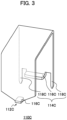
- FIG. 3 is a diagram showing a shape example in which the feeding point contact portion 112 of the metal plate antenna 110 according to the present embodiment has the bent portion 116 and the GND contact portion 114 has the bent portion 116 and the pin portions 118.
- a feeding point contact portion 112C having a bent portion 116C formed by bending one end of an arch shape of a metal plate antenna 110C is provided at the one end.
- a GND contact portion 114C having a bent portion 116C formed by bending the other end of the arch shape of the metal plate antenna 110C and two pin portions 118C inserted into the through holes 155 formed in the substrate 150 is provided at the other end.
- the bent portion 116C of the feeding point contact portion 112C and the bent portion 116C of the GND contact portion 114C are fixed to the substrate 150 with a conductive adhesive.
- the two pin portions 118C of the GND contact portion 114C do not need to be fixed to the substrate 150 with a conductive adhesive.
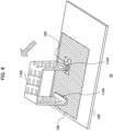
- FIG. 4 is a diagram for explaining the GND contact portion 114C included in the metal plate antenna 110C according to the present embodiment.
- FIG. 4 shows a positional relationship between the bent portion 116C and the pin portion 118C of the GND contact portion 114C and the substrate 150.
- FIG. 4 partial regions of the metal plate antenna 110C and the substrate 150 are shown enlarged, and illustration of other regions is omitted.
- the bent portion 116C of the GND contact portion 114C comes into contact with an upper surface of the substrate 150. Also, the bent portion 116C of the GND contact portion 114C is fixed to the substrate 150 with a conductive adhesive. In addition, as shown in FIG. 5 , the GND 130 is formed in a region in contact with the GND contact portion 114 on the upper surface of the substrate 150.
- the pin portion 118C of the GND contact portion 114C is inserted into the through hole 155 formed in the substrate 150, but may not come into contact with the substrate 150.
- the pin portion 118C of the GND contact portion 114C may be formed such that a portion protruding from a lower surface of the substrate 150 tapers toward its tip.
- pin portion 118C of the GND contact portion 114C is that it is not fixed to the substrate 150 with a conductive adhesive.
- the pin portion 118C is inserted into the through hole 155 formed in the substrate 150, it is possible to prevent occurrence of a positional deviation between the substrate 150 and the metal plate antenna 110C during the manufacturing process and prevent the metal plate antenna 110C from being unable to stand on its own on the substrate 150 and falling down.
- the pin portion 118C is not fixed to the substrate 150 with a conductive adhesive, it is possible to prevent various defects (for example, soldering defects) that may occur with the fixing process using the conductive adhesive.
- the shape of the metal plate antenna 110 according to the present embodiment has been described above with specific examples.
- the shapes described with reference to FIGS. 1 to 4 are merely examples, and the shape of the metal plate antenna 110 according to the present embodiment is not limited to such examples.
- the number of the pin portions 118 formed on the metal plate antenna 110 is not limited to the examples shown in FIGS. 2 and 3 .
- areas of the bent portions 116 formed in the metal plate antenna 110 are not limited to the examples shown in FIGS. 1 and 3 .
- bent portions 116 formed in the metal plate antenna 110 may be bent toward the outside of the arch shape, unlike the examples shown in FIGS. 1 and 3 .
- the shape of the metal plate antenna 110 according to the present embodiment can be flexibly deformed depending on a size, a material, or the like of the metal plate antenna 110.
- the antenna device 10 includes the substrate 150, the metal plate antenna 110 disposed on the substrate 150, and the feeding point 120 and the GND 130 formed on the substrate 150.
- FIG. 5 is a diagram for explaining a positional relationship among the metal plate antenna 110, the feeding point 120, the GND 130, and the substrate 150 according to the present embodiment.
- the feeding point 120 and the GND 130 are formed on the upper surface of the substrate 150.
- the GND 130 may be, for example, a solid GND or the like. Also, arrangement and an area of the GND shown in FIG. 5 are merely examples.
- the metal plate antenna 110 is disposed on the upper surface of the substrate 150 so that the feeding point contact portion 112 comes into contact with the feeding point 120 and the GND contact portion 114 comes into contact with the GND 130.
- FIG. 5 shows an example in a case in which the antenna device 10 includes the metal plate antenna 110A shown in FIG. 1 .
- the antenna device 10 further includes a high frequency IC 160 (see FIG. 6 ) connected to the feeding point 120 via a transmission line, and a notch filter that attenuates a signal in a specified frequency band.
- a high frequency IC 160 see FIG. 6
- a notch filter that attenuates a signal in a specified frequency band.
- connection and disconnection between the transmission line connecting the high frequency IC 160 to the feeding point 120 and the notch filter may be switchable by an element 180.
- FIG. 6 is a diagram for explaining an arrangement relationship among the feeding point 120, the high frequency IC 160, the notch filter, and the element 180 according to the present embodiment.
- FIG. 6 shows an example in a case in which the notch filter is a stub 170.
- a length D1 of the stub 170 is designed in accordance with a frequency serving as an attenuation target.
- the specified communication standard is ultra-wideband wireless communication.
- the ultra-wideband wireless communication a plurality of channels are specified, but available channels may be restricted depending on a country or a region.
- the antenna device 10 used in country Y is required not to transmit or receive a signal on CH5.
- the antenna device 10 may be capable of changing a frequency band of the radio signal to be transmitted and received during the manufacturing process or after manufacturing.
- the length D1 of the stub 170 is formed with a length that attenuates the signal in the frequency band corresponding to CH5.
- connection and disconnection between the transmission line connecting the high frequency IC 160 to the feeding point 120 and the stub 170 may be switchable by, for example, presence or absence of a chip element.
- the chip element is an example of the element 180.
- the chip element connects the transmission line, which connects the high frequency IC 160 to the feeding point 120, to the stub 170, and the stub 170 attenuates the signal in the frequency band corresponding to CH5, thereby making CH5 unusable.
- the antenna device 10 according to the present embodiment can easily change the available channels by performing switching between presence and absence of the chip element in the manufacturing process.
- the element 180 according to the present embodiment may be a switching element.
- one of features of the antenna device 10 according to the present embodiment is that it changes the usable frequency band by performing switching between connection and disconnection between the transmission line connecting the high frequency IC 160 to the feeding point 120 and the stub 170 using the element 180.
- each of the number of notch filters and the number of elements 180 is one has been exemplified in the above, but the number of notch filters and the number of elements 180 are not limited to these examples.
- the number of notch filters and the number of elements 180 may be designed in accordance with the number of frequency bands to be restricted.
- the antenna device 10 may not necessarily be designed to support a plurality of channels such as CH5 and CH9.
- the antenna length of the metal plate antenna 110 may be designed to match a 0.5 ⁇ resonance mode with the CH9 band, or the antenna length may be designed to match a 0.25 ⁇ resonance mode with the CH9 band.
- the metal plate antenna 110 may be disposed at a position on the substrate corresponding to a polarized wave to be received.
- FIGS. 7 and 8 are diagrams for explaining a distribution of a current flowing through the metal plate antenna 110 in accordance with its position on the substrate and a direction of a polarized wave in accordance with the distribution of the current.
- FIGS. 7 and 8 the direction of the current is indicated by dot arrows, and the direction of the polarized wave is indicated by a hatched arrow.
- FIG. 7 shows an example in a case in which the metal plate antenna 110A is disposed near a center of the substrate 150.
- the polarized wave associated with the metal plate antenna 110 becomes a vertically polarized wave, and the metal plate antenna 110 can receive only a vertically polarized wave.
- FIG. 8 shows an example in a case in which the metal plate antenna 110A is disposed near a corner of the substrate 150.
- the current flowing parallel to the substrate 150 on the upper surface of the metal plate antenna 110A increases.
- the polarized wave associated with the metal plate antenna 110 is greatly tilted from the vertical, and the metal plate antenna 110 can receive not only the vertical polarized wave but also a horizontally polarized wave.
- the metal plate antenna 110 receives a polarized wave transmitted by a smartphone is assumed.
- smartphones are often placed horizontally on a desk or placed in a pocket or bag in a near-vertical state, smartphones are highly likely to transmit both horizontal and vertical polarized waves.
- the antenna device 10 may be disposed near a corner of the substrate 150 as shown in FIG. 8 .
- one of the factors that change a polarized wave of the metal plate antenna 110 in accordance with its position on the substrate 150 may be asymmetry of a current flowing through the GND 130.
- the GND 130 according to the present embodiment may be formed in a pattern corresponding to the polarized wave received by the metal plate antenna 110.
- the basic description of the metal plate antenna 110 according to the present embodiment has been given above. Next, modified examples of the metal plate antenna 110 according to the present embodiment will be described.
- bent portion 116 a modified example of the bent portion 116 will be described.
- the shape of the bent portion according to the present embodiment is not limited to such an example.
- FIG. 9 is a schematic diagram for explaining a modified example of the bent portion 116 according to the present embodiment. Also, although FIG. 9 shows a modified example of the metal plate antenna 110A, a similar modified example can be applied to the metal plate antenna 110C.
- the bent portion 116A may be bent toward the outside of the arch shape.
- the bent portion 116A may be bent toward the outside of the arch shape and then further bent in a substantially vertical direction.
- the metal plate antenna 110A according to the present embodiment may not have the bent portion 116A, as shown in the lower part of FIG. 9 .
- the metal plate antenna 110A can also stand on its own on the substrate 150 by fixing it with a conductive adhesive such as solder.
- the metal plate antenna 110 may have opening portions 210 in the vicinity of a position immediately above the bent portion 116.
- FIG. 10 is a diagram for explaining the opening portions 210 formed in the vicinity of the portion immediately above the bent portion 116. Also, although FIG. 10 shows a modified example of the metal plate antenna 110A, a similar modified example can be applied to the metal plate antenna 110C.
- the metal plate antenna 110A is formed using a metal material, it has high thermal conductivity. For this reason, at the time of fixing with a conductive adhesive such as solder, heat tends to escape upward from the bent portion 116A.
- opening portions 210A are formed in the vicinity of the portion immediately above the bent portion 116A, it is possible to effectively prevent heat from escaping upward from the bent portion 116A, and to efficiently perform fixing with a conductive adhesive such as solder.
- the metal plate antenna 110 may have a structure for detouring the current, such as slits 220.
- FIGS. 11 and 12 are diagrams for explaining the slits 220 according to the present embodiment. Also, although FIGS. 11 and 12 show modified examples of the metal plate antenna 110A, similar modified examples are applicable to the metal plate antennas 110B and 110C.
- the metal plate antenna 110A may have one or a plurality of slits 220A in the upper surface or a side surface (a side surface on the feeding point contact portion 112A side (a feeding side surface) or a side surface on the GND contact portion 114A side (a GND side surface)).
- the current flows to detour around the slits 220A, which makes it possible to secure a longer antenna length defined by the length between the feeding point contact portion 112A and the GND contact portion 114A.
- FIG. 11 illustrates the case in which the plurality of slits 220A are formed in the same direction
- a formation pattern of the slits 220A according to the present embodiment is not limited to this example.
- the slits 220A according to the present embodiment may be formed in two opposing directions, for example, as shown in the upper and lower parts of FIG. 12 .
- the structure for detouring the current formed in the metal plate antenna 110 is not limited to the slits 220.
- the structure may be the opening portions 210.
- FIG. 13 is a diagram for explaining the opening portions 210 as a structure for detouring the current. Also, although FIG. 13 shows a modified example of the metal plate antenna 110A, a similar modified example is applicable to the metal plate antennas 110B and 110C.
- the metal plate antenna 110A may have one or a plurality of opening portions 210A in the upper surface or the side surface (the feeding side surface or the GND side surface).
- the current flows to detour around the opening portions 210A, which makes it possible to secure a longer antenna length defined by the length between the feeding point contact portion 112A and the GND contact portion 114A.
- the slits 220 and the opening portions 210 as structures for detouring the current have been described above. Formation patterns of the slits 220 and the opening portions 210 may be appropriately designed in accordance with a desired antenna length, a size of the metal plate antenna 110, or the like.
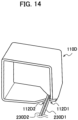
- a metal plate antenna 110D shown in FIG. 14 has two feeding point contact portions 112D1 and 112D2 while not having the GND contact portion 114.
- Each of two feeding point contact portions 112D1 and 112D2 is connected to a feeding wiring 230D1(+) or a feeding wiring 230D2(-) provided on the substrate 150.
- the metal plate antenna 110D can operate as a one-wavelength loop antenna without a mirror image effect of the GND 130.
- the metal plate antenna 110D may be electrically connected to the feeding wiring 230D via a metal foil pattern 190 (indicated by a lattice pattern) formed on the substrate 150.
- the metal foil pattern 190 may be made of copper foil or the like, for example.
- the metal plate antenna 110D can also operate as a one-wavelength loop antenna without the mirror image effect of the GND 130.
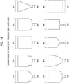
- FIG. 16 is a diagram showing variation examples of the shape of the feeding side surface of the metal plate antenna 110 according to the present embodiment.
- the feeding side surface of the metal plate antenna 110 according to the present embodiment may be formed such that a width W2 of a lower end thereof coming into contact with the feeding point 120 is narrower than a width W1 of an upper end thereof.
- the width W2 of the lower end may be approximately the same as the width W1 of the upper end, as illustrated in the lower right end of FIG. 16 .
- FIG. 17 is a diagram showing a formation example of the stubs 240 according to the present embodiment. Also, although FIG. 17 shows a modified example of the metal plate antenna 110A, a similar modified example is applicable to the metal plate antennas 110B and 110C.
- the metal plate antenna 110 may have one or a plurality of stubs 240A on one or a plurality of surfaces of the GND side surface, the upper surface, and the feeding side surface.
- the stubs 240A may be formed to extend in a direction substantially perpendicular to a direction connecting the feeding point contact portion 112Ato the GND contact portion 114A.
- the metal plate antenna 110A function as a circular polarized wave antenna.
- the stub 240A may be formed to extend in the direction substantially perpendicular to the direction connecting the feeding point contact portion 112A to the GND contact portion 114A, and then further extend toward the feeding point contact portion 112A or the GND contact portion 114A.
- the stubs 240A may be bent, for example, at locations indicated by two-dot chain lines in FIG. 17 .
- the stubs 240 According to the stubs 240 according to the present embodiment, it is possible to efficiently adjust the polarized wave and the antenna length.
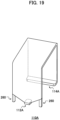
- FIG. 18 is a diagram showing examples of the mold structure according to the present embodiment. Also, although FIG. 18 shows modified examples of the metal plate antenna 110A, similar modified examples can be applied to the metal plate antennas 110B and 110C.
- an insulating material 250 may be filled inside the arch shape of the metal plate antenna 110A according to the present embodiment.
- the metal plate antenna 110A may be covered with the insulating material 250 on the outside in addition to the inside of the arch shape.
- the support portions 260 are configured to support the metal plate antenna 110 to be self-standing on the substrate 150.
- FIG. 19 is a diagram for explaining a shape example of the support portions 260 according to the present embodiment. Also, although FIG. 19 shows a modified example of the metal plate antenna 110A, a similar modified example can be applied to the metal plate antennas 110B and 110C.
- the metal plate antenna 110A may have one or a plurality of support portions 260.
- FIG. 19 illustrates the case in which the support portions 260 are disposed on the feeding side surface, but the support portions 260 may be formed to connect the upper surface of the metal plate antenna 110A to the substrate 150.
- the metal plate antenna 110A can more stably stand on its own on the substrate 150.
- the metal plate antenna 110 according to the present embodiment is configured of one metal plate has been mainly described.
- the metal plate antenna 110 may be configured of a plurality of metal plates.
- FIG. 20 is a diagram for explaining the metal plate antenna 110 configured of a plurality of metal plates according to the present embodiment. Also, although FIG. 20 shows a modified example of the metal plate antenna 110A, a similar modified example can be applied to the metal plate antennas 110B and 110C.
- the metal plate antenna 110A may be configured of a metal plate 110A1 and a metal plate 110A2.
- the region between the metal plate 110A1 and the metal plate 110A2 is not DC-conducting, the region operates as a capacitor, and thus high frequency conduction is realized, and the function of the metal plate antenna 110A as an antenna is also realized.
- the region between the metal plates 110A1 and 110A2 may be filled with the insulating material 250, for example, as shown in FIG. 20 .
- a metal plate antenna that has an arch shape and transmits and receives a radio signal based on a specified communication standard, comprising: a feeding point contact portion configured to come into contact with a feeding point formed on a substrate at one end of the arch shape; and a GND contact portion configured to come into contact with a GND formed on the substrate at the other end of the arch shape, wherein an antenna length defined by a length between the feeding point contact portion and the GND contact portion is formed to be approximately 1/2 of a wavelength of the radio signal based on the specified communication standard.
Landscapes
- Engineering & Computer Science (AREA)
- Computer Networks & Wireless Communication (AREA)
- Signal Processing (AREA)
- Details Of Aerials (AREA)
- Support Of Aerials (AREA)
Abstract
Description
- This application is based upon and claims benefit of priority from
Japanese Patent Application No. 2022-107295, filed on July 1, 2022 Japanese Patent Application No. 2022-160863, filed on October 5, 2022 Japanese Patent Application No. 2023-011971, filed on January 30, 2023 - The present invention relates to a metal plate antenna and an antenna device.
- In recent years, a wide variety of antennas have been developed. For example, Non-Patent Document 1 discloses a disk monopole antenna disposed on a substrate.
- [Non-Patent Document 1] Satoshi Honda, three others, "A DISK MONOPOLE ANTENNA WITH 1:8 IMPEDANCE BANDWIDTH AND OMNIDIRECTIONAL RADIATION PATTERN," [online], September 25, 1992, PROCEEDINGS OF ISAP '92, SAPPORO, JAPAN, [accessed January 30, 2023], Internet <https://citeseerx.ist.psu.edu/pdf/ca777261654e94c97cf6965fb24f6c4a52a1 09a2>
- The disk monopole antenna disclosed in Non-Patent Document 1 lacks stability because it has a structure that stands vertically on a substrate with a single support point. In a case in which the antenna has such a structure, there is a possibility that the antenna may fall down or the like due to an impact or the like during the manufacturing process or after the product has been shipped and may not function.
- Thus, an object of the present invention is to provide an antenna that can be stably disposed on a substrate.
- To solve the above described problem, according to an aspect of the present invention, there is provided a metal plate antenna that has an arch shape and transmits and receives a radio signal based on a specified communication standard, comprising: a feeding point contact portion configured to come into contact with a feeding point formed on a substrate at one end of the arch shape; and a GND contact portion configured to come into contact with a GND formed on the substrate at the other end of the arch shape, wherein an antenna length defined by a length between the feeding point contact portion and the GND contact portion is formed to be approximately 1/2 of a wavelength of the radio signal based on the specified communication standard.
- To solve the above described problem, according to another aspect of the present invention, there is provided an antenna device comprising: a substrate; a feeding point formed on the substrate; a GND formed on the substrate; a high frequency IC disposed on the substrate; a notch filter formed on the substrate and attenuating a signal in a specified frequency band; and a metal plate antenna that has an arch shape, is disposed on the substrate, and transmits and receives a radio signal based on a specified communication standard, wherein connection and disconnection between a transmission line connecting the high frequency IC to the feeding point and the notch filter is switchable by an element, the metal plate antenna includes: a feeding point contact portion configured to come into contact with a feeding point formed on the substrate at one end of the arch shape; and a GND contact portion configured to come into contact with the GND formed on the substrate at the other end of the arch shape, and an antenna length defined by a length between the feeding point contact portion and the GND contact portion is formed to be approximately 1/2 of a wavelength of the radio signal based on the specified communication standard.
- To solve the above described problem, according to another aspect of the present invention, there is provided an antenna device comprising: a substrate; a feeding point formed on the substrate; a GND formed on the substrate; and a metal plate antenna that has an arch shape, is disposed on the substrate, and transmits and receives a radio signal based on a specified communication standard, wherein the metal plate antenna includes: a feeding point contact portion configured to come into contact with a feeding point formed on the substrate at one end of the arch shape; and a GND contact portion configured to come into contact with the GND formed on the substrate at the other end of the arch shape, an antenna length thereof defined by a length between the feeding point contact portion and the GND contact portion is formed to be approximately 1/2 of a wavelength of the radio signal based on the specified communication standard, and the metal plate antenna is disposed at a position on the substrate in accordance with a received polarized wave.
- As described above, according to the present invention, it is possible to provide an antenna that can be stably disposed on a substrate.
-
-
FIG. 1 is a diagram showing a shape example in a case in which both a feeding point contact portion 112 and a GND contact portion 114 of a metal plate antenna 110 according to the present embodiment have bent portions 116. -
FIG. 2 is a diagram showing a shape example in a case in which both the feeding point contact portion 112 and the GND contact portion 114 of the metal plate antenna 110 according to the same embodiment have pin portions 118. -
FIG. 3 is a diagram showing a shape example in a case in which the feeding point contact portion 112 of the metal plate antenna 110 according to the same embodiment has the bent portion 116, and the GND contact portion 114 has the bent portion 116 and the pin portions 118. -
FIG. 4 is a diagram for explaining theGND contact portion 114C included in the metal plate antenna 110. -
FIG. 5 is a diagram for explaining a positional relationship among the metal plate antenna 110, afeeding point 120, aGND 130, and asubstrate 150 according to the same embodiment. -
FIG. 6 is a diagram for explaining an arrangement relationship among thefeeding point 120, ahigh frequency IC 160, a notch filter, and anelement 180 according to the same embodiment. -
FIG. 7 is a diagram for explaining a distribution of a current flowing through the metal plate antenna 110 in accordance with its position on the substrate and a direction of a polarized wave in accordance with the distribution of the current according to the same embodiment. -
FIG. 8 is a diagram for explaining the distribution of the current flowing through the metal plate antenna 110 in accordance with the position on the substrate and the direction of the polarized wave in accordance with the distribution of the current according to the same embodiment. -
FIG. 9 is a schematic diagram for explaining a modified example of the bent portions 116 according to the same embodiment. -
FIG. 10 is a diagram for explaining opening portions 210 formed in the vicinity immediately above the bent portion 116 according to the same embodiment. -
FIG. 11 is a diagram for explaining slits 220 according to the same embodiment. -
FIG. 12 is a diagram for explaining the slits 220 according to the same embodiment. -
FIG. 13 is a diagram for explaining the opening portions 210 as a structure for detouring the current according to the same embodiment. -
FIG. 14 is a diagram for explaining a modified example of the metal plate antenna 110 having two feeding point contact portions 112 according to the same embodiment. -
FIG. 15 is a diagram for explaining the metal plate antenna 110 electrically connected to a feeding wiring 230D via ametal foil pattern 190 according to the same embodiment. -
FIG. 16 is a diagram showing variation examples of a shape of a feeding side surface of the metal plate antenna 110 according to the same embodiment. -
FIG. 17 is a diagram showing a formation example of stubs 240 according to the same embodiment. -
FIG. 18 is a diagram showing examples of a mold structure according to the same embodiment. -
FIG. 19 is a diagram for explaining a shape example ofsupport portions 260 according to the same embodiment. -
FIG. 20 is a diagram for explaining the metal plate antenna 110 formed from a plurality of metal plates according to the same embodiment. - Hereinafter, referring to the appended drawings, preferred embodiments of the present invention will be described in detail. It should be noted that, in this specification and the appended drawings, structural elements that have substantially the same function and structure are denoted with the same reference numerals, and repeated explanation thereof is omitted.
- In addition, in this specification and the appended drawings, letters may be added to ends of reference numerals when a plurality of configurations of the same type are described separately. On the other hand, in a case in which there is no need to distinguish the plurality of configurations of the same type from each other, the letters may be omitted and a description that commonly applies to all of the plurality of configurations of the same type may be given.
- First, a metal plate antenna 110 provided in an antenna device 10 (see
FIG. 5 ) according to one embodiment of the present invention will be described. - The metal plate antenna 110 according to the present embodiment transmits and receives a radio signal based on a specified communication standard.
- Examples of the specified communication standard according to the present embodiment include, for example, ultra-wide band (UWB) wireless communication.
- On the other hand, the specified communication standard according to the present embodiment is not limited to the above example. Any communication standard may be adopted as the specified communication standard according to the present embodiment.
- Also, the metal plate antenna 110 according to the present embodiment is conceived by focusing on stable placement on the substrate 150 (see
FIG. 5 ) and has a characteristic shape that will be described below. - The metal plate antenna 110 according to the present embodiment is made of, for example, one metal plate and is formed to have an arch shape in at least a portion thereof.
- In addition, the metal plate antenna 110 according to the present embodiment has a feeding point contact portion 112 (
FIGS. 1 to 3 and5 ) that comes into contact with a feeding point 120 (seeFIG. 5 ) formed on thesubstrate 150 at one end of the arch shape. - Further, the metal plate antenna 110 according to the present embodiment includes a GND contact portion 114 (see
FIGS. 1 to 5 ) that comes into contact with a GND 130 (seeFIG. 5 ) formed on thesubstrate 150 at another end (the other end) of the arch shape different from the one end. - That is, the metal plate antenna 110 according to the present embodiment is supported by the feeding point contact portion 112 and the GND contact portion 114 on the
substrate 150. - According to the above configuration, the metal plate antenna 110 can be disposed more stably on the
substrate 150 as compared with a case in which an antenna is supported by a single support point. - Also, the feeding point contact portion 112 and the GND contact portion 114 may be fixed to the
substrate 150 with a conductive adhesive such as solder in order to further improve stability. However, some GND contact portions 114 do not need to be fixed with a conductive adhesive as will be described later. - Further, an antenna length defined by a length between the feeding point contact portion 112 and the GND contact portion 114 according to the present embodiment is formed to be approximately 1/2 of a wavelength λ of the radio signal based on the specified communication standard.
- In a case in which the antenna length is formed as above, the metal plate antenna 110 operates as a one-wavelength (λ) loop antenna due to a mirror image formed with the
GND 130 as a mirror surface. - Next, a shape of the feeding point contact portion 112 and a shape of the GND contact portion 114 according to the present embodiment will be described in detail.
- At least one of the feeding point contact portion 112 and the GND contact portion 114 according to the present embodiment may have a bent portion 116 formed by bending an end portion of the arch shape.
-
FIG. 1 is a diagram showing a shape example in a case in which both the feeding point contact portion 112 and the GND contact portion 114 of the metal plate antenna 110 according to the present embodiment have the bent portions 116. - In the case of the example shown in
FIG. 1 , the arch shape of ametal plate antenna 110A is formed in a U shape. - A feeding
point contact portion 112A having abent portion 116A formed by bending one end of the arch shape of themetal plate antenna 110A is provided at the one end. - Similarly, a
GND contact portion 114A having abent portion 116A formed by bending the other end of the arch shape of themetal plate antenna 110A is provided at the other end. - Since the feeding
point contact portion 112A and theGND contact portion 114A have thebent portions 116A, their contact areas with thefeeding point 120 and theGND 130 are increased, and stability of themetal plate antenna 110A on thesubstrate 150 is further improved. - In addition, since the
bent portion 116A has a large contact area with thefeeding point 120 or theGND 130, there is an advantage that a fillet is easily formed in fixing with a conductive adhesive such as solder, and the formed fillet is easily confirmed. - Also, since the
bent portion 116A has a large contact area with thefeeding point 120 or theGND 130, wiring is easily drawn out. - On the other hand, at least one of the feeding point contact portion 112 and the GND contact portion 114 according to the present embodiment may have at least one pin portion 118 that is inserted into a through hole 155 (see
FIG. 5 ) formed in thesubstrate 150. -
FIG. 2 is a diagram showing a shape example in which both the feeding point contact portion 112 and the GND contact portion 114 of the metal plate antenna 110 according to the present embodiment have the pin portions 118. - In the case of the example shown in
FIG. 2 , a feedingpoint contact portion 112B having onepin portion 118B inserted into the throughhole 155 formed in thesubstrate 150 is provided at one end of an arch shape of ametal plate antenna 110B. - A
GND contact portion 114B having threepin portions 118B inserted into the throughholes 155 formed in thesubstrate 150 is provided at the other end of the arch shape of themetal plate antenna 110B. - Since each of the feeding
point contact portion 112B and theGND contact portion 114B has one ormore pin portions 118B, themetal plate antenna 110B is more firmly fixed to thesubstrate 150, and it is possible to reduce a possibility of themetal plate antenna 110B falling down or being displaced, for example, in a reflow process or the like as well. - In addition, the
pin portion 118B of the feedingpoint contact portion 112B is fixed to thesubstrate 150 with a conductive adhesive. - Further, at least one of the
pin portions 118B of theGND contact portion 114B is fixed to thesubstrate 150 with a conductive adhesive. For example, as shown inFIG. 2 , in a case in which theGND contact portion 114B has threepin portions 118B, only onepin portion 118B may be fixed to thesubstrate 150 with a conductive adhesive, and the remaining twopin portions 118B may not be fixed in the same manner. - The shape example in which both the feeding point contact portion 112 and the GND contact portion 114 of the metal plate antenna 110 have the pin portions 118 has been described above. On the other hand, the feeding point contact portion 112 according to the present embodiment may have a bent portion 116 and the GND contact portion 114 may have a bent portion 116 and one or more pin portions 118.
-
FIG. 3 is a diagram showing a shape example in which the feeding point contact portion 112 of the metal plate antenna 110 according to the present embodiment has the bent portion 116 and the GND contact portion 114 has the bent portion 116 and the pin portions 118. - In the case of the example shown in
FIG. 3 , a feedingpoint contact portion 112C having abent portion 116C formed by bending one end of an arch shape of ametal plate antenna 110C is provided at the one end. - Also, a
GND contact portion 114C having abent portion 116C formed by bending the other end of the arch shape of themetal plate antenna 110C and twopin portions 118C inserted into the throughholes 155 formed in thesubstrate 150 is provided at the other end. - As shown in
FIG. 3 , in a case in which themetal plate antenna 110C has both thebent portion 116C and thepin portions 118C at end portions of the arch shape, it is possible to enjoy both the effect of the bent portion 116 and the effect of the pin portion 118 described above. - Further, in the case of the
metal plate antenna 110C shown inFIG. 3 , thebent portion 116C of the feedingpoint contact portion 112C and thebent portion 116C of theGND contact portion 114C are fixed to thesubstrate 150 with a conductive adhesive. - On the other hand, the two
pin portions 118C of theGND contact portion 114C do not need to be fixed to thesubstrate 150 with a conductive adhesive. -
FIG. 4 is a diagram for explaining theGND contact portion 114C included in themetal plate antenna 110C according to the present embodiment.FIG. 4 shows a positional relationship between thebent portion 116C and thepin portion 118C of theGND contact portion 114C and thesubstrate 150. Also, inFIG. 4 , partial regions of themetal plate antenna 110C and thesubstrate 150 are shown enlarged, and illustration of other regions is omitted. - As shown in
FIG. 4 , thebent portion 116C of theGND contact portion 114C comes into contact with an upper surface of thesubstrate 150. Also, thebent portion 116C of theGND contact portion 114C is fixed to thesubstrate 150 with a conductive adhesive. In addition, as shown inFIG. 5 , theGND 130 is formed in a region in contact with the GND contact portion 114 on the upper surface of thesubstrate 150. - On the other hand, as shown in
FIG. 4 , thepin portion 118C of theGND contact portion 114C is inserted into the throughhole 155 formed in thesubstrate 150, but may not come into contact with thesubstrate 150. - In addition, the
pin portion 118C of theGND contact portion 114C may be formed such that a portion protruding from a lower surface of thesubstrate 150 tapers toward its tip. - Further, one of features of the
pin portion 118C of theGND contact portion 114C is that it is not fixed to thesubstrate 150 with a conductive adhesive. - Since the
pin portion 118C is inserted into the throughhole 155 formed in thesubstrate 150, it is possible to prevent occurrence of a positional deviation between thesubstrate 150 and themetal plate antenna 110C during the manufacturing process and prevent themetal plate antenna 110C from being unable to stand on its own on thesubstrate 150 and falling down. - In addition, since the
pin portion 118C is not fixed to thesubstrate 150 with a conductive adhesive, it is possible to prevent various defects (for example, soldering defects) that may occur with the fixing process using the conductive adhesive. - The shape of the metal plate antenna 110 according to the present embodiment has been described above with specific examples.
- However, the shapes described with reference to
FIGS. 1 to 4 are merely examples, and the shape of the metal plate antenna 110 according to the present embodiment is not limited to such examples. - For example, the number of the pin portions 118 formed on the metal plate antenna 110 is not limited to the examples shown in
FIGS. 2 and3 . - Also, for example, areas of the bent portions 116 formed in the metal plate antenna 110 are not limited to the examples shown in
FIGS. 1 and3 . - In addition, for example, the bent portions 116 formed in the metal plate antenna 110 may be bent toward the outside of the arch shape, unlike the examples shown in
FIGS. 1 and3 . - The shape of the metal plate antenna 110 according to the present embodiment can be flexibly deformed depending on a size, a material, or the like of the metal plate antenna 110.
- Next, a configuration example of the
antenna device 10 according to the present embodiment will be described. - As described above, the
antenna device 10 according to the present embodiment includes thesubstrate 150, the metal plate antenna 110 disposed on thesubstrate 150, and thefeeding point 120 and theGND 130 formed on thesubstrate 150. -
FIG. 5 is a diagram for explaining a positional relationship among the metal plate antenna 110, thefeeding point 120, theGND 130, and thesubstrate 150 according to the present embodiment. - As shown in
FIG. 5 , thefeeding point 120 and theGND 130 are formed on the upper surface of thesubstrate 150. - The
GND 130 may be, for example, a solid GND or the like. Also, arrangement and an area of the GND shown inFIG. 5 are merely examples. - Further, the metal plate antenna 110 is disposed on the upper surface of the
substrate 150 so that the feeding point contact portion 112 comes into contact with thefeeding point 120 and the GND contact portion 114 comes into contact with theGND 130. - Also,
FIG. 5 shows an example in a case in which theantenna device 10 includes themetal plate antenna 110A shown inFIG. 1 . - Next, another configuration included in the
antenna device 10 according to the present embodiment will be described. - The
antenna device 10 according to the present embodiment further includes a high frequency IC 160 (seeFIG. 6 ) connected to thefeeding point 120 via a transmission line, and a notch filter that attenuates a signal in a specified frequency band. - Also, connection and disconnection between the transmission line connecting the
high frequency IC 160 to thefeeding point 120 and the notch filter may be switchable by anelement 180. -
FIG. 6 is a diagram for explaining an arrangement relationship among thefeeding point 120, thehigh frequency IC 160, the notch filter, and theelement 180 according to the present embodiment. - Also,
FIG. 6 shows an example in a case in which the notch filter is astub 170. - A length D1 of the
stub 170 is designed in accordance with a frequency serving as an attenuation target. - For example, it is assumed that the specified communication standard is ultra-wideband wireless communication. In the ultra-wideband wireless communication, a plurality of channels are specified, but available channels may be restricted depending on a country or a region.
- For example, if CH5 and CH9 are available in country X, but only CH9 is available in country Y, the
antenna device 10 used in country Y is required not to transmit or receive a signal on CH5. - In view of the circumstances as described above, the
antenna device 10 according to the present embodiment may be capable of changing a frequency band of the radio signal to be transmitted and received during the manufacturing process or after manufacturing. - For example, in the case of the example given above, the length D1 of the
stub 170 is formed with a length that attenuates the signal in the frequency band corresponding to CH5. - Also, connection and disconnection between the transmission line connecting the
high frequency IC 160 to thefeeding point 120 and thestub 170 may be switchable by, for example, presence or absence of a chip element. Further, the chip element is an example of theelement 180. - In a case in which the
antenna device 10 includes the chip element, the chip element connects the transmission line, which connects thehigh frequency IC 160 to thefeeding point 120, to thestub 170, and thestub 170 attenuates the signal in the frequency band corresponding to CH5, thereby making CH5 unusable. - On the other hand, in a case in which the
antenna device 10 does not have the chip element, a state in which the transmission line connecting thehigh frequency IC 160 to thefeeding point 120 is not connected to thestub 170 is maintained, and attenuation of the signal in the frequency band corresponding to CH5 is not performed by thestub 170, and thus both CHS and CH9 can be used. - In this way, the
antenna device 10 according to the present embodiment can easily change the available channels by performing switching between presence and absence of the chip element in the manufacturing process. - On the other hand, the
element 180 according to the present embodiment may be a switching element. - In this case, it is possible to change the available channels by performing switching between connection and disconnection between the transmission line connecting the
high frequency IC 160 and thefeeding point 120 and thestub 170 using the switching element. - Also, in this case, it is possible to switch the available channels even after the product is shipped, thereby increasing versatility.
- As described above, one of features of the
antenna device 10 according to the present embodiment is that it changes the usable frequency band by performing switching between connection and disconnection between the transmission line connecting thehigh frequency IC 160 to thefeeding point 120 and thestub 170 using theelement 180. - According to the above feature, it is possible to easily respond to changes in destinations, or the like, and to significantly reduce costs.
- Also, the case in which each of the number of notch filters and the number of
elements 180 is one has been exemplified in the above, but the number of notch filters and the number ofelements 180 are not limited to these examples. - The number of notch filters and the number of
elements 180 may be designed in accordance with the number of frequency bands to be restricted. - On the other hand, the
antenna device 10 according to the present embodiment may not necessarily be designed to support a plurality of channels such as CH5 and CH9. - For example, the antenna length of the metal plate antenna 110 may be designed to match a 0.5λ resonance mode with the CH9 band, or the antenna length may be designed to match a 0.25λ resonance mode with the CH9 band.
- Next, arrangement of the metal plate antenna 110 according to the present embodiment will be described in more detail.
- The metal plate antenna 110 according to the present embodiment may be disposed at a position on the substrate corresponding to a polarized wave to be received.
-
FIGS. 7 and8 are diagrams for explaining a distribution of a current flowing through the metal plate antenna 110 in accordance with its position on the substrate and a direction of a polarized wave in accordance with the distribution of the current. - Also, in
FIGS. 7 and8 , the direction of the current is indicated by dot arrows, and the direction of the polarized wave is indicated by a hatched arrow. -
FIG. 7 shows an example in a case in which themetal plate antenna 110A is disposed near a center of thesubstrate 150. - In this case, as shown in
FIG. 7 , almost no current flows parallel to thesubstrate 150 on an upper surface of themetal plate antenna 110A, and a current flowing perpendicularly to thesubstrate 150 becomes dominant. - As a result, the polarized wave associated with the metal plate antenna 110 becomes a vertically polarized wave, and the metal plate antenna 110 can receive only a vertically polarized wave.
- On the other hand,
FIG. 8 shows an example in a case in which themetal plate antenna 110A is disposed near a corner of thesubstrate 150. - In this case, unlike the case in which the
metal plate antenna 110A is disposed near the center of thesubstrate 150, the current flowing parallel to thesubstrate 150 on the upper surface of themetal plate antenna 110A increases. - As a result, the polarized wave associated with the metal plate antenna 110 is greatly tilted from the vertical, and the metal plate antenna 110 can receive not only the vertical polarized wave but also a horizontally polarized wave.
- Here, for example, a case in which the metal plate antenna 110 receives a polarized wave transmitted by a smartphone is assumed.
- In general, since smartphones are often placed horizontally on a desk or placed in a pocket or bag in a near-vertical state, smartphones are highly likely to transmit both horizontal and vertical polarized waves.
- For this reason, in the case of assuming reception of polarized waves from a device such as a smartphone, the
antenna device 10 according to the present embodiment may be disposed near a corner of thesubstrate 150 as shown inFIG. 8 . - Also, one of the factors that change a polarized wave of the metal plate antenna 110 in accordance with its position on the
substrate 150 may be asymmetry of a current flowing through theGND 130. For this reason, theGND 130 according to the present embodiment may be formed in a pattern corresponding to the polarized wave received by the metal plate antenna 110. - The basic description of the metal plate antenna 110 according to the present embodiment has been given above. Next, modified examples of the metal plate antenna 110 according to the present embodiment will be described.
- First, a modified example of the bent portion 116 will be described. Although the case in which the bent portion 116 according to the present embodiment is bent toward the inside of the arch shape has been described above as a main example, the shape of the bent portion according to the present embodiment is not limited to such an example.
-
FIG. 9 is a schematic diagram for explaining a modified example of the bent portion 116 according to the present embodiment. Also, althoughFIG. 9 shows a modified example of themetal plate antenna 110A, a similar modified example can be applied to themetal plate antenna 110C. - As shown in the upper part of
FIG. 9 , thebent portion 116A according to the present embodiment may be bent toward the outside of the arch shape. - Further, as shown in the middle part of
FIG. 9 , thebent portion 116A according to the present embodiment may be bent toward the outside of the arch shape and then further bent in a substantially vertical direction. - In this case, there is an advantage that a fillet is easily formed in fixing with a conductive adhesive such as solder, and the formed fillet is easily confirmed.
- On the other hand, the
metal plate antenna 110A according to the present embodiment may not have thebent portion 116A, as shown in the lower part ofFIG. 9 . - In this case, the
metal plate antenna 110A can also stand on its own on thesubstrate 150 by fixing it with a conductive adhesive such as solder. - In addition, in a case in which the metal plate antenna 110 has the bent portion 116, the metal plate antenna 110 may have opening portions 210 in the vicinity of a position immediately above the bent portion 116.
-
FIG. 10 is a diagram for explaining the opening portions 210 formed in the vicinity of the portion immediately above the bent portion 116. Also, althoughFIG. 10 shows a modified example of themetal plate antenna 110A, a similar modified example can be applied to themetal plate antenna 110C. - Since the
metal plate antenna 110A is formed using a metal material, it has high thermal conductivity. For this reason, at the time of fixing with a conductive adhesive such as solder, heat tends to escape upward from thebent portion 116A. - However, as shown in
FIG. 10 , in a case in which openingportions 210A are formed in the vicinity of the portion immediately above thebent portion 116A, it is possible to effectively prevent heat from escaping upward from thebent portion 116A, and to efficiently perform fixing with a conductive adhesive such as solder. - Next, modified examples related to securing the antenna length will be described.
- In order to secure a target antenna length, the metal plate antenna 110 according to the present embodiment may have a structure for detouring the current, such as slits 220.
-
FIGS. 11 and12 are diagrams for explaining the slits 220 according to the present embodiment. Also, althoughFIGS. 11 and12 show modified examples of themetal plate antenna 110A, similar modified examples are applicable to themetal plate antennas - As shown in
FIG. 11 , themetal plate antenna 110A according to the present embodiment may have one or a plurality ofslits 220A in the upper surface or a side surface (a side surface on the feedingpoint contact portion 112A side (a feeding side surface) or a side surface on theGND contact portion 114A side (a GND side surface)). - As shown in
FIG. 11 , in a case in which themetal plate antenna 110A has theslits 220A, the current flows to detour around theslits 220A, which makes it possible to secure a longer antenna length defined by the length between the feedingpoint contact portion 112A and theGND contact portion 114A. - Also, although
FIG. 11 illustrates the case in which the plurality ofslits 220A are formed in the same direction, a formation pattern of theslits 220A according to the present embodiment is not limited to this example. - The
slits 220A according to the present embodiment may be formed in two opposing directions, for example, as shown in the upper and lower parts ofFIG. 12 . - Also, the structure for detouring the current formed in the metal plate antenna 110 is not limited to the slits 220. The structure may be the opening portions 210.
-
FIG. 13 is a diagram for explaining the opening portions 210 as a structure for detouring the current. Also, althoughFIG. 13 shows a modified example of themetal plate antenna 110A, a similar modified example is applicable to themetal plate antennas - As shown in
FIG. 13 , themetal plate antenna 110A according to the present embodiment may have one or a plurality of openingportions 210A in the upper surface or the side surface (the feeding side surface or the GND side surface). - As shown in
FIG. 13 , in a case in which themetal plate antenna 110A has the openingportions 210A, the current flows to detour around the openingportions 210A, which makes it possible to secure a longer antenna length defined by the length between the feedingpoint contact portion 112A and theGND contact portion 114A. - The slits 220 and the opening portions 210 as structures for detouring the current have been described above. Formation patterns of the slits 220 and the opening portions 210 may be appropriately designed in accordance with a desired antenna length, a size of the metal plate antenna 110, or the like.
- Next, a modified example of the metal plate antenna 110 having two feeding point contact portions 112 will be described with reference to
FIG. 14 . - A
metal plate antenna 110D shown inFIG. 14 has two feeding point contact portions 112D1 and 112D2 while not having the GND contact portion 114. - Each of two feeding point contact portions 112D1 and 112D2 is connected to a feeding wiring 230D1(+) or a feeding wiring 230D2(-) provided on the
substrate 150. - According to the above configuration, the
metal plate antenna 110D can operate as a one-wavelength loop antenna without a mirror image effect of theGND 130. - Also, as shown in
FIG. 15 , themetal plate antenna 110D may be electrically connected to the feeding wiring 230D via a metal foil pattern 190 (indicated by a lattice pattern) formed on thesubstrate 150. Further, themetal foil pattern 190 may be made of copper foil or the like, for example. In this case, themetal plate antenna 110D can also operate as a one-wavelength loop antenna without the mirror image effect of theGND 130. - In the above, the modified examples regarding securing the antenna length have been explained. Next, modified examples regarding a shape of the feeding side surface will be described.
-
FIG. 16 is a diagram showing variation examples of the shape of the feeding side surface of the metal plate antenna 110 according to the present embodiment. - The feeding side surface of the metal plate antenna 110 according to the present embodiment may be formed such that a width W2 of a lower end thereof coming into contact with the
feeding point 120 is narrower than a width W1 of an upper end thereof. - According to the above shape, the effect of facilitating impedance matching can be obtained.
- However, in a case in which impedance can be matched by other means, the width W2 of the lower end may be approximately the same as the width W1 of the upper end, as illustrated in the lower right end of
FIG. 16 . - Next, a modified example in a case in which the metal plate antenna 110 according to the present embodiment has stubs 240 will be described.
-
FIG. 17 is a diagram showing a formation example of the stubs 240 according to the present embodiment. Also, althoughFIG. 17 shows a modified example of themetal plate antenna 110A, a similar modified example is applicable to themetal plate antennas - As shown in
FIG. 17 , the metal plate antenna 110 according to the present embodiment may have one or a plurality ofstubs 240A on one or a plurality of surfaces of the GND side surface, the upper surface, and the feeding side surface. - As shown in the upper part of
FIG. 17 , thestubs 240A may be formed to extend in a direction substantially perpendicular to a direction connecting the feeding point contact portion 112Ato theGND contact portion 114A. - According to the
stubs 240A formed as described above, it is possible to further flow a current in a direction perpendicular to the current flow shown inFIGS. 7 and8 to make themetal plate antenna 110A function as a circular polarized wave antenna. - Alternatively, as shown in the lower part of
FIG. 17 , thestub 240A may be formed to extend in the direction substantially perpendicular to the direction connecting the feedingpoint contact portion 112A to theGND contact portion 114A, and then further extend toward the feedingpoint contact portion 112A or theGND contact portion 114A. - Also, the
stubs 240A may be bent, for example, at locations indicated by two-dot chain lines inFIG. 17 . - According to the stubs 240 according to the present embodiment, it is possible to efficiently adjust the polarized wave and the antenna length.
- Next, a mold structure according to the present embodiment will be described.
-
FIG. 18 is a diagram showing examples of the mold structure according to the present embodiment. Also, althoughFIG. 18 shows modified examples of themetal plate antenna 110A, similar modified examples can be applied to themetal plate antennas - As shown in the upper part of
FIG. 18 , an insulatingmaterial 250 may be filled inside the arch shape of themetal plate antenna 110A according to the present embodiment. - Alternatively, as shown in the lower part of
FIG. 18 , themetal plate antenna 110A according to the present embodiment may be covered with the insulatingmaterial 250 on the outside in addition to the inside of the arch shape. - According to such a mold structure using the insulating
material 250, it is possible to effectively prevent a change in the shape of themetal plate antenna 110A. - Next, a modified example in which the metal plate antenna 110 according to the present embodiment has
support portions 260 will be described. - The
support portions 260 according to the present embodiment are configured to support the metal plate antenna 110 to be self-standing on thesubstrate 150. -
FIG. 19 is a diagram for explaining a shape example of thesupport portions 260 according to the present embodiment. Also, althoughFIG. 19 shows a modified example of themetal plate antenna 110A, a similar modified example can be applied to themetal plate antennas - As shown in
FIG. 19 , themetal plate antenna 110A according to the present embodiment may have one or a plurality ofsupport portions 260. - Further,
FIG. 19 illustrates the case in which thesupport portions 260 are disposed on the feeding side surface, but thesupport portions 260 may be formed to connect the upper surface of themetal plate antenna 110A to thesubstrate 150. - According to the
support portions 260 according to the present embodiment, themetal plate antenna 110A can more stably stand on its own on thesubstrate 150. - Next, a modified example of the metal plate according to the present embodiment will be described.
- In the above, the case in which the metal plate antenna 110 according to the present embodiment is configured of one metal plate has been mainly described.
- On the other hand, the metal plate antenna 110 according to the present embodiment may be configured of a plurality of metal plates.
-
FIG. 20 is a diagram for explaining the metal plate antenna 110 configured of a plurality of metal plates according to the present embodiment. Also, althoughFIG. 20 shows a modified example of themetal plate antenna 110A, a similar modified example can be applied to themetal plate antennas - As shown in
FIG. 20 , themetal plate antenna 110A according to the present embodiment may be configured of a metal plate 110A1 and a metal plate 110A2. - Although a region between the metal plate 110A1 and the metal plate 110A2 is not DC-conducting, the region operates as a capacitor, and thus high frequency conduction is realized, and the function of the
metal plate antenna 110A as an antenna is also realized. - Further, the region between the metal plates 110A1 and 110A2 may be filled with the insulating
material 250, for example, as shown inFIG. 20 . - In this case, it is possible to more stably maintain the shape (structure) of the
metal plate antenna 110A. - Heretofore, preferred embodiments of the present invention have been described in detail with reference to the appended drawings, but the present invention is not limited thereto. It should be understood by those skilled in the art that various changes and alterations may be made without departing from the spirit and scope of the appended claims.
There is provided a metal plate antenna that has an arch shape and transmits and receives a radio signal based on a specified communication standard, comprising: a feeding point contact portion configured to come into contact with a feeding point formed on a substrate at one end of the arch shape; and a GND contact portion configured to come into contact with a GND formed on the substrate at the other end of the arch shape, wherein an antenna length defined by a length between the feeding point contact portion and the GND contact portion is formed to be approximately 1/2 of a wavelength of the radio signal based on the specified communication standard.
Claims (19)
- A metal plate antenna that has an arch shape and transmits and receives a radio signal based on a specified communication standard, comprising:a feeding point contact portion configured to come into contact with a feeding point formed on a substrate at one end of the arch shape; anda GND contact portion configured to come into contact with a GND formed on the substrate at the other end of the arch shape,wherein an antenna length defined by a length between the feeding point contact portion and the GND contact portion is formed to be approximately 1/2 of a wavelength of the radio signal based on the specified communication standard.
- The metal plate antenna according to claim 1, wherein at least one of the feeding point contact portion and the GND contact portion includes a bent portion formed by bending an end portion of the arch shape.
- The metal plate antenna according to claim 1, wherein at least one of the feeding point contact portion and the GND contact portion includes at least one pin portion inserted into a through hole formed in the substrate.
- The metal plate antenna according to claim 1, wherein the feeding point contact portion and the GND contact portion include bent portions formed by bending an end portion of the arch shape.
- The metal plate antenna according to claim 1, wherein each of the feeding point contact portion and the GND contact portion includes at least one pin portion inserted into a through hole formed in the substrate.
- The metal plate antenna according to claim 1,wherein the feeding point contact portion includes a bent portion formed by bending an end portion of the arch shape, andthe GND contact portion includes a bent portion and at least one pin portion inserted into a through hole formed in the substrate.
- The metal plate antenna according to claim 6, wherein at least one of the pin portions is not fixed to the substrate with a conductive adhesive.
- The metal plate antenna according to any one of claims 1 to 7, wherein the specified communication standard includes ultra-wideband wireless communication.
- The metal plate antenna according to claim 1, further comprising a slit or an opening portion in the arch shape.
- The metal plate antenna according to claim 1, further comprising a stub in the arch shape.
- The metal plate antenna according to claim 1, wherein a width of a lower end of a side surface on the feeding point contact portion side of the arch shape is formed to be narrower than a width of an upper end thereof.
- The metal plate antenna according to claim 1, wherein an inside of the arch shape is filled with an insulating material.
- The metal plate antenna according to claim 1, further comprising a support portion configured to support the metal plate antenna to be self-standing on the substrate.
- The metal plate antenna according to claim 1, wherein the arch shape is formed by a plurality of metal plates.
- An antenna device comprising:a substrate;a feeding point formed on the substrate;a GND formed on the substrate;a high frequency IC disposed on the substrate;a notch filter formed on the substrate and attenuating a signal in a specified frequency band; anda metal plate antenna that has an arch shape, is disposed on the substrate, and transmits and receives a radio signal based on a specified communication standard,wherein connection and disconnection between a transmission line connecting the high frequency IC to the feeding point and the notch filter is switchable by an element,the metal plate antenna includes:a feeding point contact portion configured to come into contact with a feeding point formed on the substrate at one end of the arch shape; anda GND contact portion configured to come into contact with the GND formed on the substrate at the other end of the arch shape, andan antenna length defined by a length between the feeding point contact portion and the GND contact portion is formed to be approximately 1/2 of a wavelength of the radio signal based on the specified communication standard.
- The antenna device according to claim 15, wherein connection and disconnection between the transmission line connecting the high frequency IC to the feeding point and the notch filter is switchable by presence or absence of a chip element.
- The antenna device according to claim 16, further comprising a switch element configured to switch connection and disconnection between the transmission line connecting the high frequency IC to the feeding point and the notch filter.
- An antenna device comprising:a substrate;a feeding point formed on the substrate;a GND formed on the substrate; anda metal plate antenna that has an arch shape, is disposed on the substrate, and transmits and receives a radio signal based on a specified communication standard,wherein the metal plate antenna includes:a feeding point contact portion configured to come into contact with a feeding point formed on the substrate at one end of the arch shape; anda GND contact portion configured to come into contact with the GND formed on the substrate at the other end of the arch shape,an antenna length thereof defined by a length between the feeding point contact portion and the GND contact portion is formed to be approximately 1/2 of a wavelength of the radio signal based on the specified communication standard, andthe metal plate antenna is disposed at a position on the substrate in accordance with a received polarized wave.
- The antenna device according to claim 18, wherein the metal plate antenna is disposed near a corner of the substrate.
Applications Claiming Priority (3)
| Application Number | Priority Date | Filing Date | Title |
|---|---|---|---|
| JP2022107295 | 2022-07-01 | ||
| JP2022160863 | 2022-10-05 | ||
| JP2023011971A JP2024006926A (en) | 2022-07-01 | 2023-01-30 | Metal plate antenna and antenna device |
Publications (3)
| Publication Number | Publication Date |
|---|---|
| EP4311025A2 true EP4311025A2 (en) | 2024-01-24 |
| EP4311025A3 EP4311025A3 (en) | 2024-03-20 |
| EP4311025B1 EP4311025B1 (en) | 2026-03-04 |
Family
ID=86692917
Family Applications (1)
| Application Number | Title | Priority Date | Filing Date |
|---|---|---|---|
| EP23177503.2A Active EP4311025B1 (en) | 2022-07-01 | 2023-06-06 | Metal plate antenna and antenna device |
Country Status (2)
| Country | Link |
|---|---|
| US (1) | US12548912B2 (en) |
| EP (1) | EP4311025B1 (en) |
Families Citing this family (2)
| Publication number | Priority date | Publication date | Assignee | Title |
|---|---|---|---|---|
| US12548912B2 (en) * | 2022-07-01 | 2026-02-10 | Kabushiki Kaisha Tokai Rika Denki Seisakusho | Metal plate antenna and antenna device |
| JP1743491S (en) * | 2023-01-30 | 2023-05-08 | antenna |
Family Cites Families (14)
| Publication number | Priority date | Publication date | Assignee | Title |
|---|---|---|---|---|
| JPH0659009B2 (en) | 1988-03-10 | 1994-08-03 | 株式会社豊田中央研究所 | Mobile antenna |
| DE19857191A1 (en) | 1998-12-11 | 2000-07-06 | Bosch Gmbh Robert | Half loop antenna |
| DE10045634B4 (en) | 2000-09-15 | 2005-08-25 | Hella Kgaa Hueck & Co. | Resonant antenna for a control device for a motor vehicle and its use |
| JP2007123982A (en) * | 2005-10-25 | 2007-05-17 | Sony Ericsson Mobilecommunications Japan Inc | Multiband compatible antenna system and communication terminal |
| CN103081220B (en) * | 2010-08-31 | 2014-12-31 | 株式会社村田制作所 | Antenna device and wireless communication apparatus |
| EP2717383A4 (en) | 2011-06-02 | 2015-06-10 | Panasonic Corp | ANTENNA FORMING DEVICE |
| FR3033449B1 (en) | 2015-03-05 | 2018-04-13 | Tdf | BROADBAND OMNIDIRECTIONAL ANTENNA STRUCTURE |
| WO2017040223A1 (en) * | 2015-08-28 | 2017-03-09 | Skyworks Solutions, Inc. | Tunable notch filter and contour tuning circuit |
| KR102467737B1 (en) * | 2018-01-03 | 2022-11-16 | 삼성전자 주식회사 | Display apparatus and antenna assembly |
| US10840596B2 (en) * | 2018-05-22 | 2020-11-17 | Plume Design, Inc. | Tunable antenna system for Bluetooth and Wi-Fi bands with electronically-reconfigurable and mechanically-identical antennas |
| DE102018218891B4 (en) * | 2018-11-06 | 2023-12-07 | Fraunhofer-Gesellschaft zur Förderung der angewandten Forschung e.V. | Three-dimensional loop antenna device |
| JP2020150424A (en) * | 2019-03-14 | 2020-09-17 | ソニーセミコンダクタソリューションズ株式会社 | Antenna device |
| US12548912B2 (en) * | 2022-07-01 | 2026-02-10 | Kabushiki Kaisha Tokai Rika Denki Seisakusho | Metal plate antenna and antenna device |
| US12407084B2 (en) * | 2022-09-06 | 2025-09-02 | Apple Inc. | Wideband antenna structures in corner of electronic device |
-
2023
- 2023-05-31 US US18/203,766 patent/US12548912B2/en active Active
- 2023-06-06 EP EP23177503.2A patent/EP4311025B1/en active Active
Non-Patent Citations (1)
| Title |
|---|
| SATOSHI HONDA: "OMNIDIRECTIONAL RADIATION PATTERN", PROCEEDINGS OF ISAP '92, 25 September 1992 (1992-09-25), Retrieved from the Internet <URL:https://citeseerx.ist.psu.edu/pdf/ca777261654e94c97cf6965fb24f6c4a52al09a2> |
Also Published As
| Publication number | Publication date |
|---|---|
| EP4311025B1 (en) | 2026-03-04 |
| EP4311025A3 (en) | 2024-03-20 |
| US12548912B2 (en) | 2026-02-10 |
| US20240006773A1 (en) | 2024-01-04 |
Similar Documents
| Publication | Publication Date | Title |
|---|---|---|
| EP3544117B1 (en) | Patch antenna | |
| JP3959068B2 (en) | Circularly polarized antenna | |
| TWI278146B (en) | Antenna and radio frequency module comprising the same | |
| US12191567B2 (en) | Antenna module and communication device equipped with the same | |
| US12548912B2 (en) | Metal plate antenna and antenna device | |
| JP2004201281A (en) | Wireless lan antenna and wireless lan card provided with the same | |
| TWI594497B (en) | Antenna having a planar conducting element with first and second end portions separated by a non-conductive gap | |
| JP2002164729A (en) | Multi-band microwave antenna | |
| US12095163B2 (en) | Antenna module and communication device equipped with the same | |
| EP2569823B1 (en) | Antenna having planar conducting elements | |
| US20220328983A1 (en) | Antenna module and communication device equipped with the same | |
| US10122093B2 (en) | Dipole array antenna | |
| US12548913B2 (en) | Inverted L antenna and antenna device | |
| JP2005020266A (en) | Multiple frequency antenna system | |
| US20100164811A1 (en) | Solid Antenna | |
| JP2004096314A (en) | Dielectric antenna and mobile communication apparatus with built-in the same | |
| EP3794680B1 (en) | Patch antenna design for easy fabrication and controllable performance at high frequency bands | |
| JP2014121014A (en) | Antenna device | |
| JPH09232854A (en) | Small planar antenna device for mobile radio | |
| WO2017022224A1 (en) | Antenna and wireless communication device | |
| JP7774041B2 (en) | antenna | |
| JP2024006926A (en) | Metal plate antenna and antenna device | |
| JP7153843B2 (en) | antenna device | |
| CN117335137A (en) | Metal plate antenna and antenna device | |
| JP4661816B2 (en) | Antenna and wireless communication device |
Legal Events
| Date | Code | Title | Description |
|---|---|---|---|
| PUAI | Public reference made under article 153(3) epc to a published international application that has entered the european phase |
Free format text: ORIGINAL CODE: 0009012 |
|
| STAA | Information on the status of an ep patent application or granted ep patent |
Free format text: STATUS: THE APPLICATION HAS BEEN PUBLISHED |
|
| AK | Designated contracting states |
Kind code of ref document: A2 Designated state(s): AL AT BE BG CH CY CZ DE DK EE ES FI FR GB GR HR HU IE IS IT LI LT LU LV MC ME MK MT NL NO PL PT RO RS SE SI SK SM TR |
|
| PUAL | Search report despatched |
Free format text: ORIGINAL CODE: 0009013 |
|
| AK | Designated contracting states |
Kind code of ref document: A3 Designated state(s): AL AT BE BG CH CY CZ DE DK EE ES FI FR GB GR HR HU IE IS IT LI LT LU LV MC ME MK MT NL NO PL PT RO RS SE SI SK SM TR |
|
| RIC1 | Information provided on ipc code assigned before grant |
Ipc: H04B 1/00 20060101ALI20240214BHEP Ipc: H01Q 9/04 20060101ALI20240214BHEP Ipc: H01Q 7/00 20060101ALI20240214BHEP Ipc: H01Q 5/25 20150101AFI20240214BHEP |
|
| STAA | Information on the status of an ep patent application or granted ep patent |
Free format text: STATUS: REQUEST FOR EXAMINATION WAS MADE |
|
| 17P | Request for examination filed |
Effective date: 20240702 |
|
| RBV | Designated contracting states (corrected) |
Designated state(s): AL AT BE BG CH CY CZ DE DK EE ES FI FR GB GR HR HU IE IS IT LI LT LU LV MC ME MK MT NL NO PL PT RO RS SE SI SK SM TR |
|
| GRAP | Despatch of communication of intention to grant a patent |
Free format text: ORIGINAL CODE: EPIDOSNIGR1 |
|
| STAA | Information on the status of an ep patent application or granted ep patent |
Free format text: STATUS: GRANT OF PATENT IS INTENDED |
|
| GRAJ | Information related to disapproval of communication of intention to grant by the applicant or resumption of examination proceedings by the epo deleted |
Free format text: ORIGINAL CODE: EPIDOSDIGR1 |
|
| STAA | Information on the status of an ep patent application or granted ep patent |
Free format text: STATUS: REQUEST FOR EXAMINATION WAS MADE |
|
| GRAJ | Information related to disapproval of communication of intention to grant by the applicant or resumption of examination proceedings by the epo deleted |
Free format text: ORIGINAL CODE: EPIDOSDIGR1 |
|
| GRAP | Despatch of communication of intention to grant a patent |
Free format text: ORIGINAL CODE: EPIDOSNIGR1 |
|
| GRAP | Despatch of communication of intention to grant a patent |
Free format text: ORIGINAL CODE: EPIDOSNIGR1 |
|
| STAA | Information on the status of an ep patent application or granted ep patent |
Free format text: STATUS: GRANT OF PATENT IS INTENDED |
|
| RIC1 | Information provided on ipc code assigned before grant |
Ipc: H01Q 5/25 20150101AFI20251031BHEP Ipc: H01Q 7/00 20060101ALI20251031BHEP Ipc: H01Q 9/04 20060101ALI20251031BHEP Ipc: H04B 1/10 20060101ALI20251031BHEP |
|
| INTG | Intention to grant announced |
Effective date: 20251117 |
|
| INTC | Intention to grant announced (deleted) | ||
| INTG | Intention to grant announced |
Effective date: 20251208 |
|
| GRAS | Grant fee paid |
Free format text: ORIGINAL CODE: EPIDOSNIGR3 |
|
| GRAA | (expected) grant |
Free format text: ORIGINAL CODE: 0009210 |
|
| STAA | Information on the status of an ep patent application or granted ep patent |
Free format text: STATUS: THE PATENT HAS BEEN GRANTED |
|
| AK | Designated contracting states |
Kind code of ref document: B1 Designated state(s): AL AT BE BG CH CY CZ DE DK EE ES FI FR GB GR HR HU IE IS IT LI LT LU LV MC ME MK MT NL NO PL PT RO RS SE SI SK SM TR |
|
| REG | Reference to a national code |
Ref country code: CH Ref legal event code: F10 Free format text: ST27 STATUS EVENT CODE: U-0-0-F10-F00 (AS PROVIDED BY THE NATIONAL OFFICE) Effective date: 20260304 Ref country code: GB Ref legal event code: FG4D |
|
| REG | Reference to a national code |
Ref country code: DE Ref legal event code: R096 Ref document number: 602023012859 Country of ref document: DE |
|
| REG | Reference to a national code |
Ref country code: IE Ref legal event code: FG4D |
|
| PG25 | Lapsed in a contracting state [announced via postgrant information from national office to epo] |
Ref country code: RS Free format text: LAPSE BECAUSE OF FAILURE TO SUBMIT A TRANSLATION OF THE DESCRIPTION OR TO PAY THE FEE WITHIN THE PRESCRIBED TIME-LIMIT Effective date: 20260604 |
|
| PG25 | Lapsed in a contracting state [announced via postgrant information from national office to epo] |
Ref country code: ES Free format text: LAPSE BECAUSE OF FAILURE TO SUBMIT A TRANSLATION OF THE DESCRIPTION OR TO PAY THE FEE WITHIN THE PRESCRIBED TIME-LIMIT Effective date: 20260304 |
|
| REG | Reference to a national code |
Ref country code: NL Ref legal event code: MP Effective date: 20260304 |
|
| PG25 | Lapsed in a contracting state [announced via postgrant information from national office to epo] |
Ref country code: PL Free format text: LAPSE BECAUSE OF FAILURE TO SUBMIT A TRANSLATION OF THE DESCRIPTION OR TO PAY THE FEE WITHIN THE PRESCRIBED TIME-LIMIT Effective date: 20260304 |
|
| PG25 | Lapsed in a contracting state [announced via postgrant information from national office to epo] |
Ref country code: GR Free format text: LAPSE BECAUSE OF FAILURE TO SUBMIT A TRANSLATION OF THE DESCRIPTION OR TO PAY THE FEE WITHIN THE PRESCRIBED TIME-LIMIT Effective date: 20260605 |
|
| REG | Reference to a national code |
Ref country code: LT Ref legal event code: MG9D |
|
| PG25 | Lapsed in a contracting state [announced via postgrant information from national office to epo] |
Ref country code: LT Free format text: LAPSE BECAUSE OF FAILURE TO SUBMIT A TRANSLATION OF THE DESCRIPTION OR TO PAY THE FEE WITHIN THE PRESCRIBED TIME-LIMIT Effective date: 20260304 |
|
| PGFP | Annual fee paid to national office [announced via postgrant information from national office to epo] |
Ref country code: DE Payment date: 20260629 Year of fee payment: 4 |
|
| PG25 | Lapsed in a contracting state [announced via postgrant information from national office to epo] |
Ref country code: NO Free format text: LAPSE BECAUSE OF FAILURE TO SUBMIT A TRANSLATION OF THE DESCRIPTION OR TO PAY THE FEE WITHIN THE PRESCRIBED TIME-LIMIT Effective date: 20260604 |
|
| PG25 | Lapsed in a contracting state [announced via postgrant information from national office to epo] |
Ref country code: SE Free format text: LAPSE BECAUSE OF FAILURE TO SUBMIT A TRANSLATION OF THE DESCRIPTION OR TO PAY THE FEE WITHIN THE PRESCRIBED TIME-LIMIT Effective date: 20260304 Ref country code: FI Free format text: LAPSE BECAUSE OF FAILURE TO SUBMIT A TRANSLATION OF THE DESCRIPTION OR TO PAY THE FEE WITHIN THE PRESCRIBED TIME-LIMIT Effective date: 20260304 |
|
| PG25 | Lapsed in a contracting state [announced via postgrant information from national office to epo] |
Ref country code: HR Free format text: LAPSE BECAUSE OF FAILURE TO SUBMIT A TRANSLATION OF THE DESCRIPTION OR TO PAY THE FEE WITHIN THE PRESCRIBED TIME-LIMIT Effective date: 20260304 |
|
| PG25 | Lapsed in a contracting state [announced via postgrant information from national office to epo] |
Ref country code: LV Free format text: LAPSE BECAUSE OF FAILURE TO SUBMIT A TRANSLATION OF THE DESCRIPTION OR TO PAY THE FEE WITHIN THE PRESCRIBED TIME-LIMIT Effective date: 20260304 |
|
| PG25 | Lapsed in a contracting state [announced via postgrant information from national office to epo] |
Ref country code: BG Free format text: LAPSE BECAUSE OF FAILURE TO SUBMIT A TRANSLATION OF THE DESCRIPTION OR TO PAY THE FEE WITHIN THE PRESCRIBED TIME-LIMIT Effective date: 20260304 |