EP4310913A1 - Semiconductor structure and preparation method therefor - Google Patents
Semiconductor structure and preparation method therefor Download PDFInfo
- Publication number
- EP4310913A1 EP4310913A1 EP22754758.5A EP22754758A EP4310913A1 EP 4310913 A1 EP4310913 A1 EP 4310913A1 EP 22754758 A EP22754758 A EP 22754758A EP 4310913 A1 EP4310913 A1 EP 4310913A1
- Authority
- EP
- European Patent Office
- Prior art keywords
- word line
- line trench
- doped area
- substrate
- area
- Prior art date
- Legal status (The legal status is an assumption and is not a legal conclusion. Google has not performed a legal analysis and makes no representation as to the accuracy of the status listed.)
- Granted
Links
Images




Classifications
-
- H—ELECTRICITY
- H10—SEMICONDUCTOR DEVICES; ELECTRIC SOLID-STATE DEVICES NOT OTHERWISE PROVIDED FOR
- H10B—ELECTRONIC MEMORY DEVICES
- H10B12/00—Dynamic random access memory [DRAM] devices
- H10B12/30—DRAM devices comprising one-transistor - one-capacitor [1T-1C] memory cells
- H10B12/48—Data lines or contacts therefor
- H10B12/488—Word lines
-
- H—ELECTRICITY
- H10—SEMICONDUCTOR DEVICES; ELECTRIC SOLID-STATE DEVICES NOT OTHERWISE PROVIDED FOR
- H10W—GENERIC PACKAGES, INTERCONNECTIONS, CONNECTORS OR OTHER CONSTRUCTIONAL DETAILS OF DEVICES COVERED BY CLASS H10
- H10W20/00—Interconnections in chips, wafers or substrates
- H10W20/40—Interconnections external to wafers or substrates, e.g. back-end-of-line [BEOL] metallisations or vias connecting to gate electrodes
- H10W20/41—Interconnections external to wafers or substrates, e.g. back-end-of-line [BEOL] metallisations or vias connecting to gate electrodes characterised by their conductive parts
- H10W20/435—Cross-sectional shapes or dispositions of interconnections
-
- H—ELECTRICITY
- H10—SEMICONDUCTOR DEVICES; ELECTRIC SOLID-STATE DEVICES NOT OTHERWISE PROVIDED FOR
- H10B—ELECTRONIC MEMORY DEVICES
- H10B12/00—Dynamic random access memory [DRAM] devices
- H10B12/01—Manufacture or treatment
- H10B12/02—Manufacture or treatment for one transistor one-capacitor [1T-1C] memory cells
- H10B12/05—Making the transistor
- H10B12/053—Making the transistor the transistor being at least partially in a trench in the substrate
-
- H—ELECTRICITY
- H10—SEMICONDUCTOR DEVICES; ELECTRIC SOLID-STATE DEVICES NOT OTHERWISE PROVIDED FOR
- H10B—ELECTRONIC MEMORY DEVICES
- H10B12/00—Dynamic random access memory [DRAM] devices
- H10B12/30—DRAM devices comprising one-transistor - one-capacitor [1T-1C] memory cells
-
- H—ELECTRICITY
- H10—SEMICONDUCTOR DEVICES; ELECTRIC SOLID-STATE DEVICES NOT OTHERWISE PROVIDED FOR
- H10B—ELECTRONIC MEMORY DEVICES
- H10B12/00—Dynamic random access memory [DRAM] devices
- H10B12/30—DRAM devices comprising one-transistor - one-capacitor [1T-1C] memory cells
- H10B12/34—DRAM devices comprising one-transistor - one-capacitor [1T-1C] memory cells the transistor being at least partially in a trench in the substrate
-
- H—ELECTRICITY
- H10—SEMICONDUCTOR DEVICES; ELECTRIC SOLID-STATE DEVICES NOT OTHERWISE PROVIDED FOR
- H10D—INORGANIC ELECTRIC SEMICONDUCTOR DEVICES
- H10D62/00—Semiconductor bodies, or regions thereof, of devices having potential barriers
- H10D62/10—Shapes, relative sizes or dispositions of the regions of the semiconductor bodies; Shapes of the semiconductor bodies
- H10D62/124—Shapes, relative sizes or dispositions of the regions of semiconductor bodies or of junctions between the regions
-
- H—ELECTRICITY
- H10—SEMICONDUCTOR DEVICES; ELECTRIC SOLID-STATE DEVICES NOT OTHERWISE PROVIDED FOR
- H10D—INORGANIC ELECTRIC SEMICONDUCTOR DEVICES
- H10D64/00—Electrodes of devices having potential barriers
- H10D64/20—Electrodes characterised by their shapes, relative sizes or dispositions
- H10D64/27—Electrodes not carrying the current to be rectified, amplified, oscillated or switched, e.g. gates
- H10D64/311—Gate electrodes for field-effect devices
- H10D64/411—Gate electrodes for field-effect devices for FETs
- H10D64/511—Gate electrodes for field-effect devices for FETs for IGFETs
- H10D64/512—Disposition of the gate electrodes, e.g. buried gates
- H10D64/513—Disposition of the gate electrodes, e.g. buried gates within recesses in the substrate, e.g. trench gates, groove gates or buried gates
-
- H—ELECTRICITY
- H10—SEMICONDUCTOR DEVICES; ELECTRIC SOLID-STATE DEVICES NOT OTHERWISE PROVIDED FOR
- H10D—INORGANIC ELECTRIC SEMICONDUCTOR DEVICES
- H10D64/00—Electrodes of devices having potential barriers
- H10D64/20—Electrodes characterised by their shapes, relative sizes or dispositions
- H10D64/27—Electrodes not carrying the current to be rectified, amplified, oscillated or switched, e.g. gates
- H10D64/311—Gate electrodes for field-effect devices
- H10D64/411—Gate electrodes for field-effect devices for FETs
- H10D64/511—Gate electrodes for field-effect devices for FETs for IGFETs
- H10D64/517—Gate electrodes for field-effect devices for FETs for IGFETs characterised by the conducting layers
- H10D64/518—Gate electrodes for field-effect devices for FETs for IGFETs characterised by the conducting layers characterised by their lengths or sectional shapes
-
- H—ELECTRICITY
- H10—SEMICONDUCTOR DEVICES; ELECTRIC SOLID-STATE DEVICES NOT OTHERWISE PROVIDED FOR
- H10P—GENERIC PROCESSES OR APPARATUS FOR THE MANUFACTURE OR TREATMENT OF DEVICES COVERED BY CLASS H10
- H10P30/00—Ion implantation into wafers, substrates or parts of devices
- H10P30/20—Ion implantation into wafers, substrates or parts of devices into semiconductor materials, e.g. for doping
- H10P30/202—Ion implantation into wafers, substrates or parts of devices into semiconductor materials, e.g. for doping characterised by the semiconductor materials
- H10P30/204—Ion implantation into wafers, substrates or parts of devices into semiconductor materials, e.g. for doping characterised by the semiconductor materials into Group IV semiconductors
-
- H—ELECTRICITY
- H10—SEMICONDUCTOR DEVICES; ELECTRIC SOLID-STATE DEVICES NOT OTHERWISE PROVIDED FOR
- H10P—GENERIC PROCESSES OR APPARATUS FOR THE MANUFACTURE OR TREATMENT OF DEVICES COVERED BY CLASS H10
- H10P30/00—Ion implantation into wafers, substrates or parts of devices
- H10P30/20—Ion implantation into wafers, substrates or parts of devices into semiconductor materials, e.g. for doping
- H10P30/208—Ion implantation into wafers, substrates or parts of devices into semiconductor materials, e.g. for doping of electrically inactive species
-
- H—ELECTRICITY
- H10—SEMICONDUCTOR DEVICES; ELECTRIC SOLID-STATE DEVICES NOT OTHERWISE PROVIDED FOR
- H10P—GENERIC PROCESSES OR APPARATUS FOR THE MANUFACTURE OR TREATMENT OF DEVICES COVERED BY CLASS H10
- H10P50/00—Etching of wafers, substrates or parts of devices
- H10P50/60—Wet etching
- H10P50/64—Wet etching of semiconductor materials
- H10P50/642—Chemical etching
-
- H—ELECTRICITY
- H10—SEMICONDUCTOR DEVICES; ELECTRIC SOLID-STATE DEVICES NOT OTHERWISE PROVIDED FOR
- H10W—GENERIC PACKAGES, INTERCONNECTIONS, CONNECTORS OR OTHER CONSTRUCTIONAL DETAILS OF DEVICES COVERED BY CLASS H10
- H10W20/00—Interconnections in chips, wafers or substrates
- H10W20/01—Manufacture or treatment
- H10W20/071—Manufacture or treatment of dielectric parts thereof
- H10W20/081—Manufacture or treatment of dielectric parts thereof by forming openings in the dielectric parts
- H10W20/089—Manufacture or treatment of dielectric parts thereof by forming openings in the dielectric parts using processes for implementing desired shapes or dispositions of the openings, e.g. double patterning
-
- H—ELECTRICITY
- H10—SEMICONDUCTOR DEVICES; ELECTRIC SOLID-STATE DEVICES NOT OTHERWISE PROVIDED FOR
- H10P—GENERIC PROCESSES OR APPARATUS FOR THE MANUFACTURE OR TREATMENT OF DEVICES COVERED BY CLASS H10
- H10P14/00—Formation of materials, e.g. in the shape of layers or pillars
- H10P14/60—Formation of materials, e.g. in the shape of layers or pillars of insulating materials
- H10P14/63—Formation of materials, e.g. in the shape of layers or pillars of insulating materials characterised by the formation processes
- H10P14/6302—Non-deposition formation processes
- H10P14/6304—Formation by oxidation, e.g. oxidation of the substrate
- H10P14/6306—Formation by oxidation, e.g. oxidation of the substrate of the semiconductor materials
- H10P14/6308—Formation by oxidation, e.g. oxidation of the substrate of the semiconductor materials of Group IV semiconductors
- H10P14/6309—Formation by oxidation, e.g. oxidation of the substrate of the semiconductor materials of Group IV semiconductors of silicon in uncombined form, i.e. pure silicon
Definitions
- the disclosure relates to the technical field of semiconductor manufacture, in particular to a semiconductor structure and a manufacturing method thereof.
- DRAM dynamic random access memory
- MOS metal oxide semiconductor
- an MOS with buried word lines is used in the memory cell transistor, which can reduce the short channel effect to a certain extent, and thus reduce the leakage phenomenon of devices.
- a semiconductor structure and a manufacturing method thereof is provided.
- a first aspect of the embodiments of the disclosure provides a manufacturing method of a semiconductor structure, and the manufacturing method includes: providing a substrate; forming an ion implantation area in the substrate, an upper surface of the ion implantation area having a distance from an upper surface of the substrate; forming an initial word line trench in the substrate; the initial word line trench extending from the upper surface of the substrate into the ion implantation area; and widening the initial word line trench to form a word line trench; a width of a bottom of the word line trench being greater than a minimum width of the word line trench.
- fluorine ions or boron ions are implanted into the substrate to form the ion implantation area.
- an ion concentration of the ion implantation area is 1 ⁇ 10 17 cm 3 to 1 ⁇ 10 22 cm 3 ; and a distance between the ion implantation area and the upper surface of the substrate is 100 nm to 200 nm.
- widening the initial word line trench to form the word line trench includes: forming a sacrificial dielectric layer on a sidewall and a bottom of the initial word line trench by an in-situ growth process; a thickness of the sacrificial dielectric layer located in the ion implantation area being greater than a thickness of the remaining sacrificial dielectric layer; and removing the sacrificial dielectric layer to form the word line trench.
- the manufacturing method of a semiconductor structure further includes: performing ion implantation a first conductive type in the substrate to eliminate the ion implantation area and form a first doped area; a bottom of the first doped area being lower than a bottom of the word line trench, and a top of the first doped area being higher than the bottom of the word line trench; performing ion implantation of a second conductive type in the substrate to form a second doped area; the second doped area being located above the first doped area and extending to the upper surface of the substrate; the word line trench penetrating the second doped area and extending into the first doped area; the first doped area being a doped area of the first conductive type, and the second doped area being a doped area of the second conductive type; forming a gate oxide layer on a sidewall and a bottom of the word line trench; forming a word line conductive layer on a surface of the gate oxide layer; a top of the
- the first conductive type is P-type; and the second conductive type is N-type.
- an ion concentration in the first doped area is 1 ⁇ 10 16 cm 3 to 1 ⁇ 10 20 cm 3 ; and an ion concentration in the second doped area is 1 ⁇ 10 16 cm 3 to 1 ⁇ 10 20 cm 3 .
- the ion implantation area is a first doped area; before the ion implantation area is formed in the substrate, and the manufacturing method of a semiconductor structure further includes: forming a second doped area in the substrate; the second doped area being located above the first doped area and extending to the upper surface of the substrate; the initial word line trench penetrating the second doped area and extending into the first doped area; the first doped area being a doped area of the first conductive type, and the second doped area being a doped area of the second conductive type.
- widening the initial word line trench to form the word line trench includes: wet etching the initial word line trench with a wet etching solution to obtain the word line trench; an etching rate of the wet etching solution to a part of the initial word line trench in the first doped area being greater than an etching rate of the wet etching solution to a part of the initial word line trench in the second doped area.
- the first conductive type is P-type; the second conductive type is N-type; the wet etch solution includes a mixture of ammonia water and hydrogen peroxide.
- an ion concentration in the first doped area is 1 ⁇ 10 16 cm 3 to 1 ⁇ 10 20 cm 3 ; and an ion concentration in the second doped area is 1 ⁇ 10 16 cm 3 to 1 ⁇ 10 20 cm 3 , and a distance between the first doped area and the upper surface of the substrate is 100 nm to 200 nm.
- the manufacturing method of a semiconductor structure further includes: forming a gate oxide layer on a sidewall and a bottom of the word line trench; forming a word line conductive layer on a surface of the gate oxide layer, a top of the word line conductive layer being lower than a top of the word line trench; and forming a filling dielectric layer in the word line trench, the filling dielectric layer being located on the top of the word line conductive layer and at least filling up the word line trench.
- another aspect of the embodiments of the disclosure provide a semiconductor structure, and the semiconductor structure includes: a substrate, a first doped area and a second doped area being provided in the substrate, the second doped area extending from a upper surface of the substrate into the substrate, the first doped area being located below the second doped area, the first doped area being a doped area of a first conductive type, and the second doped area being a doped area of a second conductive type; and a word line trench, the word line trench penetrating the second doped area and extending into the first doped area, and a width of a bottom of the word line trench being greater than a minimum width of the word line trench.
- an ion concentration in the first doped area is 1 ⁇ 10 16 cm 3 to 1 ⁇ 10 20 cm 3 ; an ion concentration in the second doped area is 1 ⁇ 10 16 cm 3 to 1 ⁇ 10 20 cm 3 ; the first conductive type is P-type; the second conductive type is N-type.
- a distance between the first doped area and the upper surface of the substrate is 100 nm to 200 nm.
- the semiconductor structure further includes: a gate oxide layer located on a sidewall and a bottom of the word line trench; a word line conductive layer located on a surface of the gate oxide layer, and a top of the word line conductive layer being lower than a top of the word line trench; and a filling dielectric layer located on the top of the word line conductive layer and at least filling up the word line trench.
- Embodiments of the present disclosure may/at least have the following advantages.
- the manufacturing method of a semiconductor structure enables the initial word line trench to be widened to form the word line trench after the initial word line trench is formed by forming an ion implantation area in the substrate, thereby increasing the cross-sectional area of the bottom of the formed word line trench, reducing the resistance of the word line formed in the subsequent manufacturing process, and avoiding the increase of power consumption of the device and the deterioration of RC delay.
- the semiconductor structure provided by the embodiments of the present disclosure has a word line trench with a larger bottom cross-sectional area, which can reduce the resistance of the word line formed in the subsequent manufacturing process, and avoid the increase of power consumption of the device and the deterioration of RC delay.
- the first element, component, region, layer, doped type, or portion discussed below may be represented as a second element, component, region, layer, or portion; for example the first doped area may be referred to as the second doped area and similarly the second doped area may be referred to as the first doped area.
- the first doped area and the second doped area are different doped areas, for example, the first doped area may be a doped area of the first conductive type and the second doped area may be a doped area of the second conductive type, or the first doped area may be a doped area of the second conductive type and the second doped area may be a doped area of the first conductive type.
- Spatial relationship terms such as “below”, “above” may be used herein to describe a relationship between one element or feature and another element or feature shown in the drawings. It should be understood, the spatial relationship terms further include different orientations of a device in use and operation in addition to the orientations shown in the drawings. For example, if the device in the drawing is turned over, an element or feature described as being “below” another element will be oriented as being “above” another element or feature. Therefore, the exemplary terms “above” may include up and down orientations. In addition, the device may also include additional orientations (e.g., rotation for 90 degrees or other orientations), and the spatial terms used herein are interpreted accordingly.
- additional orientations e.g., rotation for 90 degrees or other orientations
- Embodiments of the disclosure are described herein with reference to cross-sectional views of schematic diagrams of ideal embodiments (and intermediate structures) as embodiments of the present disclosure, so that variations of the illustrated shape caused by, for example, manufacturing techniques and/or tolerances can be anticipated.
- embodiments of the present disclosure should not be limited to the specific shape of the areas shown herein but include shape deviations caused by for example manufacturing techniques.
- the areas shown in the figure are schematic in nature and their shapes do not represent the actual shape of the areas of the device and do not limit the scope of the disclosed embodiments.
- FIGs. 1 to 15 illustrate only schematically the basic concept of the embodiments of the present disclosure. Although only the components related to the embodiment of the present disclosure are shown in the drawings and the drawings are not drawn according to the number, shape and size of the components in actual implementation, the shape, number and proportion of the components in actual implementation may be an arbitrary change, and the layout type of the components may be more complex.
- a buried word line is used in the memory cell transistor, which can reduce the short channel effect to a certain extent, and thus reduce the leakage phenomenon of devices.
- an island structure is usually formed in the substrate 1' by dry etching; then a chevron trench of the buried word line is formed by dry etching; after that, a thermal oxidation process is performed to form a gate oxide layer 132', and then metal 133' is deposited and the dielectric layer 134' is formed sequentially from bottom to top to form a word line structure, as shown in FIG.2 .
- the size of the memory cell decreases, the size of the buried word line trench will also decrease, and then the cross-sectional area of the metal filled in the buried word line trench will also decrease, which will lead to an increase in the resistance of the word line, resulting in more power consumption and aggravating RC delay.
- a manufacturing method of a semiconductor structure is provided.
- the manufacturing method may include the following operations.
- an ion implantation area is formed in the substrate, and an upper surface of the ion implantation area has a distance from an upper surface of the substrate.
- an initial word line trench is formed in the substrate, and the initial word line trench extends from the upper surface of the substrate to the ion implantation area.
- the initial word line trench is widened to form a word line trench, and the width of the bottom of the word line trench is greater than the minimum width of the word line trench.
- the manufacturing method of a semiconductor structure provided by the embodiments of the present disclosure, by forming the ion implantation area in the substrate, it enables the initial word line trench to be widened to form the word line trench after the initial word line trench is formed, thereby increasing the cross-sectional area of the bottom of the formed word line trench, and reducing the resistance of the word line formed in the subsequent manufacturing process, and thus reducing the power consumption of the device and decreasing the RC delay.
- the substrate 1 is provided.
- the material of the substrate 1 is not specifically limited.
- the substrate 1 may include, but is not limited to, one or more of a silicon substrate, a sapphire substrate, a glass substrate, a silicon carbide substrate, a gallium nitride substrate, a gallium arsenide substrate or the like, that is, the material of the substrate 1 may include but is not limited to one or more of silicon, sapphire, glass, silicon carbide, gallium nitride, gallium arsenide or the like.
- the manufacturing method may further include the operation of etching the initial substrate to form the island structure as shown in FIG. 4 .
- the initial substrate may be etched by but not limited to dry etching.
- an ion implantation area 11 is formed in the substrate 1. Specifically, there is a distance between the upper surface of the ion implantation area 11 and the upper surface of the substrate 1.
- the ion concentration of the ion implantation area 11 is not specifically limited.
- the ion concentration of the ion implantation area 11 may be 1 ⁇ 10 17 cm 3 to 1 ⁇ 10 22 cm 3 ; for example, the ion concentration of the ion implantation area 11 may be 1 ⁇ 10 17 cm 3 , 1 ⁇ 10 18 cm 3 , 1 ⁇ 10 19 cm 3 , 1 ⁇ 10 20 cm 3 , 1 ⁇ 10 21 cm 3 or 1 ⁇ 10 22 cm 3 or the like.
- the distance between the ion implantation area 11 and the upper surface of the substrate 1 is not specifically limited.
- the distance between the ion implantation area 11 and the upper surface of the substrate 1 may be 100 nm to 200 nm; for example the distance between the ion implantation area 11 and the upper surface of the substrate 1 may be 100 nm, 125 nm, 150 nm, 175 nm, or 200 nm.
- an initial word line trench 12 is formed in the substrate 1. Specifically, the initial word line trench 12 extends from the upper surface of the substrate 1 to the ion implantation area 11.
- Embodiments of the present disclosure do not specifically limit the method for forming the initial word line trench 12.
- the initial word line trench 12 may be formed in the substrate 1 by, but not limited to dry etching.
- the operation of forming the initial word line trench 12 in the silicon substrate may be performed by, for example dry etching the silicon substrate with carbon tetrafluoride (CF 4 ) as an etching gas, in which the carbon tetrafluoride will be dissociated into trifluoromethyl (CF 3 ) and fluorine (F) neutral groups in capacitive coupled plasma (CCP) or inductively coupled plasma (ICP).
- CF 4 carbon tetrafluoride
- F fluorine neutral groups
- CCP capacitive coupled plasma
- ICP inductively coupled plasma
- Embodiments of the present disclosure do not specifically limit the width of the initial word line trench 12.
- the width of the initial word line trench 12 formed in S2 may be 1/3 to 2/3 of the width of the word line trench 13 formed in the subsequent process; for example, the width of the initial word line trench 12 formed in S2 may be 1/3, 1/2 or 2/3 of the width of the word line trench 13 formed in the subsequent process or the like.
- embodiments of the present disclosure do not specifically limit the depth of the initial word line trench 12.
- the bottom of the initial word line trench 12 may be located in the ion implantation area 11.
- the initial word line trench 12 is widened to form the word line trench 13.
- the width d1 of the bottom of the word line trench 13 should be greater than the minimum width d2 of the word line trench 13.
- the minimum width of the word line trench 13 may also be the width of the upper part of the word line trench 13 (the area above the bottom of the word line trench 13), for example, the upper part of the word line trench 13 is rectangular.
- the method for widening the initial word line trench 12 is not specifically limited.
- S4 may include the following operations.
- a sacrificial dielectric layer 131 is formed on the sidewall and the bottom of the initial word line trench 12 by an in-situ growth process; specifically, the thickness of the sacrificial dielectric layer 131 in the ion implantation area 11 should be greater than the thickness of the remaining sacrificial dielectric layer 131.
- the method of the in-situ growth process for forming the sacrificial dielectric layer 131 is not specifically limited.
- the exposed sidewall and bottom of the initial word line trench 12 should include silicon (Si).
- the operation of forming the sacrificial dielectric layer 131 on the sidewall and the bottom of the initial word line trench 12 may be performed as follows, for example, the exposed silicon after etching is oxidized to silicon dioxide (SiO 2 ) by thermal oxidation (e.g. dry oxygen oxidation or wet oxygen oxidation) process to form the sacrificial dielectric layer 131.
- silicon in the initial word line trench 12 in the ion implantation area 11 has a faster reaction rate, more silicon can be consumed, so that the thickness of the sacrificial dielectric layer 131 formed in the ion implantation area 11 is greater than the thickness of the remaining sacrificial dielectric layer 131.
- the type of ions implanted in the ion implantation area 11 is not specifically limited.
- the ion implantation area 11 may be formed by implanting fluorine ions into the substrate 1. Implanting fluorine ions into the substrate 1 can reduce the activation energy of silicon and oxygen (O) elements, and form Si-F bonds with lower activity than Si-Si bonds, that is, Si-F bonds are more easily broken, that is, oxygen is easier to break Si-F bonds to forms Si-O bonds.
- the formed ion implantation area 11 has a faster oxidation rate, which can consume more silicon, and helps to promote the formation of a thicker sacrificial dielectric layer 131.
- the operation of implanting fluorine ions into the substrate 1 to form the ion implantation area 11 may be performed as follows.
- boron trifluoride (BF 3 ) is used as an ion source, and accelerated into a mass analyzer by an electric field after being ionized.
- Fluoride ions (F+ or F++) are sorted out by the magnetic field of the mass analyzer, the energy of fluoride ion is allowed to reach 120 KeV through the accelerator, and the ion implantation area 11 with doped concentration being 1 ⁇ 10 17 cm 3 to 1 ⁇ 10 22 cm 3 in an area with a depth of 100 nm to 200 nm from the upper surface of the substrate 1 is formed.
- the method for removing the sacrificial dielectric layer 131 is not specifically limited.
- the sacrificial dielectric layer 131 may be removed by but not limited to wet etching.
- the type of wet etching solution used in S402 is not specifically limited.
- the sacrificial dielectric layer 131 may be completely removed by using but not limited to diluted hydrofluoric acid (DHF) or buffered oxide etch (BOE).
- DHF diluted hydrofluoric acid
- BOE buffered oxide etch
- the manufacturing method may include the following operations.
- ion implantation of a first conductive type is performed in the substrate 1 to eliminate the ion implantation area 11 and form a first doped area 141; specifically, the bottom of the first doped area 141 should be lower than the bottom of the word line trench 13, and the top of the first doped area 141 should be higher than the bottom of the word line trench 13.
- ion implantation of a second conductive type is performed in the substrate 1 to form a second doped area 142; specifically, as shown in FIG. 11 , the second doped area 142 should be located above the first doped area 141 and extend to the upper surface of the substrate 1; meanwhile, the word line trench 13 should penetrate the second doped area 142 and extend into the first doped area 141; the first doped area 141 is a doped area of the first conductive type, and the second doped area 142 is a doped area of the second conductive type.
- a gate oxide layer 132 is formed on the sidewall and the bottom of the word line trench 13.
- a word line conductive layer 133 is formed on the surface of the gate oxide layer 132; specifically, the top of the word line conductive layer 133 should be lower than the top of the word line trench 13.
- a filling dielectric layer 134 is formed in the word line trench 13; specifically, as shown in FIG. 13 , the filling dielectric layer 134 should be located at the top of the word line conductive layer 133 and fill up at least the word line trench 13.
- Embodiments of the present disclosure do not specifically limit the method for forming the gate oxide layer 132.
- the gate oxide layer 132 may be formed on the sidewall and the bottom of the word line trench 13 by any one of but not limited to free radical oxidation, physical vapor deposition (PVD), chemical vapor deposition (CVD), flowable chemical vapor deposition (FCVD), high density plasma deposition (HDP), plasma enhanced deposition or atomic layer deposition, or the like.
- the gate oxide layer 132 may include but is not limited to one or more of a silicon dioxide layer, a high-k dielectric material layer, or other dielectric material layer; that is, the material of the gate oxide layer 132 may include but is not limited to one or more of silicon dioxide, high-K dielectric materials, or other dielectric materials.
- the gate oxide layer 132 may be formed using free radical oxidation process at 850°C to 1050°C; for example, the gate oxide layer 132 may be formed by free radical oxidation process at 850°C, 900°C, 950°C, 1000°C, 1050°C or the like.
- Oxygen neutral radical group (O*) or hydrogen oxygen neutral radical group (OH*) is an intermediate product during forming water with hydrogen (H 2 ) and oxygen (O 2 ), which has stronger chemical activity because of the unsaturated extranulear electron. Free radicals can break weaker chemical bonds and then stronger chemical bonds are formed, and thus the gate oxide layer 132 with a higher quality can be obtained.
- the reaction pressure can be controlled within 20Torr, and the low pressure allows a longer mean free path of gas molecules, so that a longer free radical lifetime can be obtained.
- the method for forming the word line conductive layer 133 is not specifically limited.
- the word line conductive layer 133 is formed on the surface of the gate oxide layer 132 by, but not limited to one or more of chemical vapor deposition, physical l vapor deposition, flowable chemical vapor deposition, high density plasma deposition, plasma enhanced deposition, atomic layer deposition, or the like.
- the operation for forming the word line conductive layer 133 on the surface of the gate oxide layer 132 may be performed as follows.
- a word line conductive material layer is formed on the surface of the gate oxide layer 132, and part of the word line conductive material layer is etched back to form the word line conductive layer 133.
- the material of the word line conductive layer 133 is not specifically limited.
- the material of the word line conductive layer 133 may include, but is not limited to, one or more of titanium nitride (TiN), titanium (Ti), tungsten silicide (Si 2 W), tungsten (W), or the like.
- the operation of forming the word line conductive layer 133 on the surface of the gate oxide layer 132 may also be performed as follows.
- tungsten is deposited to form a word line conductive material layer using a chemical vapor deposition process with better step coverage, in which the reactant gas may include, but is not limited to, silane (SiH 4 ) and tungsten hexafluoride (WF 6 ).
- the word line conductive material layer is etched back by dry etching, in which the etching gas may be, but is not limited to, sulfur hexafluoride.
- the method for forming the filling dielectric layer 134 is not specifically limited.
- the filling dielectric layer 134 may be formed in the word line trench 13 by, but not limited to any one of chemical vapor deposition or chemical vapor deposition.
- the material of the filling dielectric layer 134 is not specifically limited.
- the material of the filling dielectric layer 134 may include, but is not limited to, one or more of silicon dioxide, silicon nitride (Si 3 N 4 ), silicon oxynitride (SiON), or the like.
- the operation of forming the filling dielectric layer 134 in the word line trench 13 may be performed as follows. For example, chemical vapor deposition is used to form silicon nitride as a filling dielectric material layer by the reaction between hexachlorodisilane (Si 2 Cl 6 , HCD) or dichlorosilane (SiH 2 Cl 2 , DCS) and ammonia (NH 3 ), and then chemical mechanical polishing (CMP) is performed to form the filling dielectric layer 134.
- CMP chemical mechanical polishing
- the first conductive type is P-type, while the second conductive type is N-type.
- the operation of forming the first doped area 141 of P-type may be performed as follows.
- the first doped area 141 of P-type doped with boron ions is formed by ion implantation using boron ions (B+) generated by ionization of boron trifluoride as an ion source.
- the operation of forming the second doped area 142 of N-type may be performed as follows.
- the second doped area 142 of N-type doped with phosphorus ions is formed above the first doped area 141 by ion implantation using phosphorus ions (P+) generated by ionization of phosphorus (P) vapor as an ion source.
- P+ phosphorus ions
- Embodiments of the present disclosure do not specifically limit the ion concentration of the first doped area 141 and the ion concentration of the second doped area 142.
- the ion concentration of the first doped area 141 may be 1 ⁇ 10 16 cm 3 to 1 ⁇ 10 20 cm 3 ; for example, the ion concentration of the first doped area 141 may be 1 ⁇ 10 16 cm 3 , 1 ⁇ 10 17 cm 3 , 1 ⁇ 10 18 cm 3 , 1 ⁇ 10 19 cm 3 , 1 ⁇ 10 20 cm 3 , or the like.
- the ion concentration of the second doped area 142 may be 1 ⁇ 10 16 cm 3 to 1 ⁇ 10 20 cm 3 ; for example, the ion concentration of the second doped area 142 may be 1 ⁇ 10 16 cm 3 , 1 ⁇ 10 17 cm 3 , 1 ⁇ 10 18 cm 3 , 1 ⁇ 10 19 cm 3 , 1 ⁇ 10 20 cm 3 or the like.
- the ion implantation area 11 may also be formed by implanting boron (B) ions into the substrate 1.
- B boron
- the ion implantation area may be reused as the first doped area 141.
- the manufacturing method may further include the operation of forming the second doped area 142 in the substrate 1.
- the second doped area 142 should be located above the first doped area 141 and extend to the upper surface of the substrate 1.
- the structure obtained in S3 may be as shown in FIG. 15 , in which the initial word line trench 12 penetrates the second doped area 142 and extends into the first doped area 142; the first doped area 141 is a doped area of the first conductive type, and the second doped area 142 is a doped area of the second conductive type.
- the width of the upper part of the initial word line trench 12 is, for example, less than 1/2 of the width of the upper part of the word line trench 13. If the width of the upper part of the initial word line trench 12 is relatively large, the width of the upper part of the initial word line trench 12 becomes larger during the subsequent widening process, such that the space between adjacent word line trenches 13 is relatively small, which is not conducive to the subsequent manufacture of bit line contact pad that is located between word line trenches 13. Because of the small space between the word line trenches 13, it is possible to cause the bit line contact pad to be connected with the word line trench 13, that is, the bit line is directly connected with the word line, thus affecting the performance of the memory.
- the first conductive type is P-type, while the second conductive type should be N-type.
- S4 may also include the following operations.
- FIG.11 is also a schematic cross-sectional structure diagram of the structure obtained after the word line trench 13 is obtained in this embodiment.
- the etching rate of the wet etching solution for part of the initial word line trench 12 in the first doped area 141 should be greater than the etching rate the wet etching solution for part of the initial word line trench 12 in the second doped area 142, so that the width of the bottom of the formed word line trench 13 can be greater than the minimum width of the word line trench 13.
- the type of the wet etching solution is not specifically limited.
- the wet etching solution may include, but is not limited to the mixture of ammonia and hydrogen peroxide (H 2 O 2 ).
- the wet etching rate of the first doped area 141 is faster, which can consume more silicon, while the wet etching rate of the second doped area 142 above the first doped area 141 is slower, which consumes less silicon. In this way, the bottom of the formed word line trench 13 is relatively wide.
- the manufacturing method may further include the following operations.
- a gate oxide layer 132 is formed on the sidewall and bottom of the word line trench 13 as shown in FIG. 12 ; a word line conductive layer 133 is formed on the surface of the gate oxide layer 132, in which the top of the word line conductive layer 133 is lower than the top of the word line trench 13; A filling dielectric layer 134 is formed in the word line trench 13, in which the filling dielectric layer 134 is located on the top of the word line conductive layer 133 and at least fills up the word line trench 13, as shown in FIG. 13 .
- FIGs. 3 , 7 , and 10 are shown in sequence as indicated by the arrows, these operations are not necessarily executed in sequence as indicated by the arrows. Unless explicitly stated herein, there are no strict sequential restrictions on the execution of these operations, and these operations can be performed in other sequences. Further, at least a part of the operations in FIGs. 3 , 7 and 10 may include a plurality of operations or stages, these operations or stages are not necessarily executed at the same time, but may be executed at different times, and the execution sequence of these operations or stages is not necessarily sequential, but may be executed in turn or alternately with other operations or at least a part of the operations or stages in other operations.
- embodiments of the present disclosure also provide a semiconductor structure.
- the semiconductor structure may include a substrate 1 and a word line trench 13.
- a first doped area 141 and a second doped area 142 is provided in the substrate 1, in which the second doped area 142 extends from the upper surface of the substrate 1 to the substrate 1; the first doped area 141 is located below the second doped area 142; specifically, the first doped area 141 may be a doped area of a first conductive type, and the second doped area 142 may be a doped area of a second conductive type.
- the word line trench 13 penetrates the second doped area 142 and extends into the first doped area 141; specifically, the width of the bottom of the word line trench 13 should be greater than the minimum width of the word line trench 13.
- the semiconductor structure of the embodiments of the present disclosure has the word line trench 143 with a larger bottom cross-sectional area, which can reduce the resistance of the word line formed in the subsequent manufacturing process, and reduce the device power consumption and decrease the RC delay.
- Embodiments of the present disclosure do not limit the distance between the first doped area 141 and the upper surface of the substrate 1.
- the distance between the first doped area 141 and the upper surface of the substrate 1 may be 100 nm to 200 nm; for example, the distance between the first doped area 141 and the upper surface of the substrate 1 may be 100nm, 125nm, 150nm, 175nm, or 200nm.
- the semiconductor structure may further include a gate oxide layer 132, a word line conductive layer 133 and a filling dielectric layer 134.
- the gate oxide layer 132 is located on the sidewall and bottom of the word line trench 13; the word line conductive layer 133 is formed on the surface of the gate oxide layer 132, and the top of the word line conductive layer 133 is lower than the top of the word line trench 13; the filling dielectric layer 134 is located on the top of the word line conductive layer 133, and at least fills up the word line trench 13.
- Embodiments in this specification are described in a progressive manner and each embodiment focuses on differences from other embodiments. As for the same and similar parts in some embodiment(s), reference can be made to other embodiment(s).
Landscapes
- Engineering & Computer Science (AREA)
- Manufacturing & Machinery (AREA)
- Semiconductor Memories (AREA)
- Insulated Gate Type Field-Effect Transistor (AREA)
- Chemical & Material Sciences (AREA)
- Chemical Kinetics & Catalysis (AREA)
- General Chemical & Material Sciences (AREA)
Abstract
Description
- The application claims priority to
Chinese Patent Application No. 202210598976.8, field before the Patent Office of China on May 30, 2022 - The disclosure relates to the technical field of semiconductor manufacture, in particular to a semiconductor structure and a manufacturing method thereof.
- As semiconductor memory devices (such as dynamic random access memory, abbreviated as DRAM) become highly integrated, the area of an unit cell on the semiconductor substrate will gradually decrease accordingly, and the length of the channel contained in a metal oxide semiconductor (MOS) transistor will gradually decrease, which will be prone to leading to short channel effect.
- In order to maintain the high integration of the semiconductor memory devices, in the current mainstream DRAM technology, an MOS with buried word lines (BWs) is used in the memory cell transistor, which can reduce the short channel effect to a certain extent, and thus reduce the leakage phenomenon of devices.
- However, as the size of the memory cell decreases, the size of a BW trench will also decrease, and then the cross-sectional area of the metal filled in the BW trench will also decrease; this will lead to an increase in the resistance of the word line (WL), resulting in more power consumption and aggravation of the signal delay (RC delay for short) caused by the charging and discharging process of the resistor (R) parasitic capacitance (C).
- According to various embodiments of the present disclosure, a semiconductor structure and a manufacturing method thereof is provided.
- According to some embodiments, a first aspect of the embodiments of the disclosure provides a manufacturing method of a semiconductor structure, and the manufacturing method includes: providing a substrate; forming an ion implantation area in the substrate, an upper surface of the ion implantation area having a distance from an upper surface of the substrate; forming an initial word line trench in the substrate; the initial word line trench extending from the upper surface of the substrate into the ion implantation area; and widening the initial word line trench to form a word line trench; a width of a bottom of the word line trench being greater than a minimum width of the word line trench.
- According to some embodiments, fluorine ions or boron ions are implanted into the substrate to form the ion implantation area.
- According to some embodiments, an ion concentration of the ion implantation area is 1 × 1017 cm3 to 1 × 1022 cm3; and a distance between the ion implantation area and the upper surface of the substrate is 100 nm to 200 nm.
- According to some embodiments, widening the initial word line trench to form the word line trench includes: forming a sacrificial dielectric layer on a sidewall and a bottom of the initial word line trench by an in-situ growth process; a thickness of the sacrificial dielectric layer located in the ion implantation area being greater than a thickness of the remaining sacrificial dielectric layer; and removing the sacrificial dielectric layer to form the word line trench.
- According to some embodiments, after the word line trench is formed, the manufacturing method of a semiconductor structure further includes: performing ion implantation a first conductive type in the substrate to eliminate the ion implantation area and form a first doped area; a bottom of the first doped area being lower than a bottom of the word line trench, and a top of the first doped area being higher than the bottom of the word line trench; performing ion implantation of a second conductive type in the substrate to form a second doped area; the second doped area being located above the first doped area and extending to the upper surface of the substrate; the word line trench penetrating the second doped area and extending into the first doped area; the first doped area being a doped area of the first conductive type, and the second doped area being a doped area of the second conductive type; forming a gate oxide layer on a sidewall and a bottom of the word line trench; forming a word line conductive layer on a surface of the gate oxide layer; a top of the word line conductive layer being lower than a top of the word line trench; and forming a filling dielectric layer in the word line trench; the filling dielectric layer being located on the top of the word line conductive layer and at least filling up the word line trench.
- According to some embodiments, the first conductive type is P-type; and the second conductive type is N-type.
- According to some embodiments, an ion concentration in the first doped area is 1 × 1016 cm3 to 1 × 1020 cm3; and an ion concentration in the second doped area is 1 × 1016 cm3 to 1 × 1020 cm3.
- According to some embodiments, the ion implantation area is a first doped area; before the ion implantation area is formed in the substrate, and the manufacturing method of a semiconductor structure further includes: forming a second doped area in the substrate; the second doped area being located above the first doped area and extending to the upper surface of the substrate; the initial word line trench penetrating the second doped area and extending into the first doped area; the first doped area being a doped area of the first conductive type, and the second doped area being a doped area of the second conductive type.
- According to some embodiments, widening the initial word line trench to form the word line trench includes: wet etching the initial word line trench with a wet etching solution to obtain the word line trench; an etching rate of the wet etching solution to a part of the initial word line trench in the first doped area being greater than an etching rate of the wet etching solution to a part of the initial word line trench in the second doped area.
- According to some embodiments, the first conductive type is P-type; the second conductive type is N-type; the wet etch solution includes a mixture of ammonia water and hydrogen peroxide.
- According to some embodiments, an ion concentration in the first doped area is 1 × 1016 cm3 to 1 × 1020 cm3; and an ion concentration in the second doped area is 1 × 1016 cm3 to 1 × 1020 cm3, and a distance between the first doped area and the upper surface of the substrate is 100 nm to 200 nm.
- According to some embodiments, after the word line trench is formed, the manufacturing method of a semiconductor structure further includes: forming a gate oxide layer on a sidewall and a bottom of the word line trench; forming a word line conductive layer on a surface of the gate oxide layer, a top of the word line conductive layer being lower than a top of the word line trench; and forming a filling dielectric layer in the word line trench, the filling dielectric layer being located on the top of the word line conductive layer and at least filling up the word line trench.
- According to some embodiments, another aspect of the embodiments of the disclosure provide a semiconductor structure, and the semiconductor structure includes: a substrate, a first doped area and a second doped area being provided in the substrate, the second doped area extending from a upper surface of the substrate into the substrate, the first doped area being located below the second doped area, the first doped area being a doped area of a first conductive type, and the second doped area being a doped area of a second conductive type; and a word line trench, the word line trench penetrating the second doped area and extending into the first doped area, and a width of a bottom of the word line trench being greater than a minimum width of the word line trench.
- According to some embodiments, an ion concentration in the first doped area is 1 × 1016 cm3 to 1 × 1020 cm3; an ion concentration in the second doped area is 1 × 1016 cm3 to 1 × 1020 cm3; the first conductive type is P-type; the second conductive type is N-type. A distance between the first doped area and the upper surface of the substrate is 100 nm to 200 nm.
- In some embodiments, the semiconductor structure further includes: a gate oxide layer located on a sidewall and a bottom of the word line trench; a word line conductive layer located on a surface of the gate oxide layer, and a top of the word line conductive layer being lower than a top of the word line trench; and a filling dielectric layer located on the top of the word line conductive layer and at least filling up the word line trench.
- Embodiments of the present disclosure may/at least have the following advantages.
- The manufacturing method of a semiconductor structure provided by the embodiments of the present disclosure enables the initial word line trench to be widened to form the word line trench after the initial word line trench is formed by forming an ion implantation area in the substrate, thereby increasing the cross-sectional area of the bottom of the formed word line trench, reducing the resistance of the word line formed in the subsequent manufacturing process, and avoiding the increase of power consumption of the device and the deterioration of RC delay.
- The semiconductor structure provided by the embodiments of the present disclosure has a word line trench with a larger bottom cross-sectional area, which can reduce the resistance of the word line formed in the subsequent manufacturing process, and avoid the increase of power consumption of the device and the deterioration of RC delay.
- The details of one or more embodiments of the disclosure are set forth in the drawings and the description below. Other features, objects and advantages of the embodiments of the disclosure will be apparent from the description, drawings and the claims.
- In order to more clearly illustrate the technical solutions of the embodiments of the disclosure, a brief description of the drawings required to be used in the description of the embodiments will be provided below. Apparently, the drawings in the following description are merely some embodiments of the disclosure. For a person of ordinary skill in the art, other drawings can be obtained based on these drawings without creative work.
-
FIG. 1 is a cross-sectional structure diagram of a structure obtained by dry etching to form a chevron trench of a buried word line in a buried word line process; -
FIG. 2 is a cross-sectional structure diagram of a structure obtained after forming a word line structure in an buried word line process; -
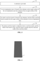
FIG. 3 is a flow chart of a manufacturing method of a semiconductor structure provided by an embodiment of the present disclosure; -
FIG. 4 is a cross-sectional structure diagram of a structure obtained by the operation S1 in the manufacturing method of a semiconductor structure provided by an embodiment of the present disclosure; -
FIG. 5 is a cross-sectional structure diagram of a structure obtained by the operation S2 in the manufacturing method of a semiconductor structure provided by an embodiment of the present disclosure; -
FIG. 6 is a cross-sectional structure diagram of a structure obtained by the operation S4 in the manufacturing method of a semiconductor structure provided by an embodiment of the present disclosure; -
FIG. 7 is a flow chart of the operation S4 in the manufacturing method of a semiconductor structure provided by an embodiment of the present disclosure; -
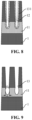
FIG. 8 is a cross-sectional structure diagram of a structure obtained by the operation S401 in the manufacturing method for a semiconductor structure provided by an embodiment of the present disclosure; -
FIG. 9 is a cross-sectional structure diagram of a structure obtained by the operation S402 in the manufacturing method of a semiconductor structure provided by an embodiment of the present disclosure; -
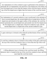
FIG. 10 is a flow chart after forming the word line trench in a manufacturing method of a semiconductor structure provided by an embodiment of the present disclosure; -
FIG. 11 is a cross-sectional structure diagram of a structure obtained by the operation S512 in the manufacturing method of a semiconductor structure provided by an embodiment of the present disclosure; -
FIG. 12 is a cross-sectional structure diagram of a structure obtained by the operation S513 in the manufacturing method of a semiconductor structure provided by an embodiment of the present disclosure; -
FIG. 13 is a cross-sectional structure diagram of a structure obtained by the operation S515 in the manufacturing method of a semiconductor structure provided by an embodiment of the present disclosure;FIG. 13 also is a cross-sectional structure diagram of a semiconductor structure provided by an embodiment of the present disclosure; -
FIG. 14 is a cross-sectional structure diagram of a structure obtained by forming a second doped area in the substrate in the manufacturing method of a semiconductor structure provided by an embodiment of the present disclosure; -
FIG. 15 is a cross-sectional structure diagram of a structure obtained by the operation S3 in the manufacturing method of a semiconductor structure provided by another embodiment of the present disclosure; - In order to facilitate to understand the embodiments of the present disclosure, a more complete description will be provided below with reference to the relative accompanying drawings. Preferred embodiments of the present disclosure are provided in the accompanying drawings. However the embodiments of the present disclosure may be implemented in many different forms and is not limited to the embodiments described herein. Rather these embodiments are provided so that the disclosure of the embodiments of the present disclosure will be more thoroughly and comprehensively understood.
- Unless otherwise defined, all technical and scientific terms used herein have the same meanings as those commonly understood by those skilled in the art of the present disclosure. Terms used herein in the specification of the present disclosure are for the purpose of describing specific embodiments only and are not intended to limit the present disclosure.
- It should be understood that when an element or a layer is referred to as "on" another element or layer, it may be directly on the other element or layer, or there may be an intermediate element or layer therebetween. It should be understood that although the terms "first", "second" and the like may be used to describe various elements, components, regions, layers, doped types and/or portions, these elements, components, regions, layers, doped types and/or portions should not be limited by these terms. These terms are only used to distinguish one element, component, region, layer, doped types or terms are only used to distinguish one element, component, region, layer, doping type or portion from another element, component, region, layer, doped types or portion. Accordingly, without departing from the teachings of the embodiments of the disclosure, the first element, component, region, layer, doped type, or portion discussed below may be represented as a second element, component, region, layer, or portion; for example the first doped area may be referred to as the second doped area and similarly the second doped area may be referred to as the first doped area. The first doped area and the second doped area are different doped areas, for example, the first doped area may be a doped area of the first conductive type and the second doped area may be a doped area of the second conductive type, or the first doped area may be a doped area of the second conductive type and the second doped area may be a doped area of the first conductive type.
- Spatial relationship terms such as "below", "above" may be used herein to describe a relationship between one element or feature and another element or feature shown in the drawings. It should be understood, the spatial relationship terms further include different orientations of a device in use and operation in addition to the orientations shown in the drawings. For example, if the device in the drawing is turned over, an element or feature described as being "below" another element will be oriented as being "above" another element or feature. Therefore, the exemplary terms "above" may include up and down orientations. In addition, the device may also include additional orientations (e.g., rotation for 90 degrees or other orientations), and the spatial terms used herein are interpreted accordingly.
- As used herein, the singular forms "a/an", "one", and "the/said" may also include the plural forms as well, unless the context clearly dictates otherwise. It should be further understood that when terms "consist of" and/or "comprise/include" used in the specification, the presence of the stated features, integers, steps, operations, elements and/or components can be determined, but the presence or addition of one or more of other features, integers, steps, operations, elements, components and/or combinations is not excluded. Meanwhile, as used herein, the term "and/or" includes any of the listed items and all combinations thereof.
- Embodiments of the disclosure are described herein with reference to cross-sectional views of schematic diagrams of ideal embodiments (and intermediate structures) as embodiments of the present disclosure, so that variations of the illustrated shape caused by, for example, manufacturing techniques and/or tolerances can be anticipated. Thus, embodiments of the present disclosure should not be limited to the specific shape of the areas shown herein but include shape deviations caused by for example manufacturing techniques. Thus the areas shown in the figure are schematic in nature and their shapes do not represent the actual shape of the areas of the device and do not limit the scope of the disclosed embodiments.
- Referring to
FIGs. 1 to 15 . It should be noted that, the drawings provided in this embodiment illustrate only schematically the basic concept of the embodiments of the present disclosure. Although only the components related to the embodiment of the present disclosure are shown in the drawings and the drawings are not drawn according to the number, shape and size of the components in actual implementation, the shape, number and proportion of the components in actual implementation may be an arbitrary change, and the layout type of the components may be more complex. - In order to maintain the high integration of the semiconductor memory devices, in the current mainstream DRAM technology, a buried word line is used in the memory cell transistor, which can reduce the short channel effect to a certain extent, and thus reduce the leakage phenomenon of devices.
- In the DRAM buried word line process, as shown in
FIG. 1 , an island structure is usually formed in the substrate 1' by dry etching; then a chevron trench of the buried word line is formed by dry etching; after that, a thermal oxidation process is performed to form a gate oxide layer 132', and then metal 133' is deposited and the dielectric layer 134' is formed sequentially from bottom to top to form a word line structure, as shown inFIG.2 . - However, as the size of the memory cell decreases, the size of the buried word line trench will also decrease, and then the cross-sectional area of the metal filled in the buried word line trench will also decrease, which will lead to an increase in the resistance of the word line, resulting in more power consumption and aggravating RC delay.
- For the deficiencies in the related art, according to some embodiments of the present disclosure, a manufacturing method of a semiconductor structure is provided.
- Referring to
FIG. 3 , in one of the embodiments, the manufacturing method may include the following operations. - In S1, a substrate is provided.
- In S2, an ion implantation area is formed in the substrate, and an upper surface of the ion implantation area has a distance from an upper surface of the substrate.
- In S3, an initial word line trench is formed in the substrate, and the initial word line trench extends from the upper surface of the substrate to the ion implantation area.
- In S4, the initial word line trench is widened to form a word line trench, and the width of the bottom of the word line trench is greater than the minimum width of the word line trench.
- In the manufacturing method of a semiconductor structure provided by the embodiments of the present disclosure, by forming the ion implantation area in the substrate, it enables the initial word line trench to be widened to form the word line trench after the initial word line trench is formed, thereby increasing the cross-sectional area of the bottom of the formed word line trench, and reducing the resistance of the word line formed in the subsequent manufacturing process, and thus reducing the power consumption of the device and decreasing the RC delay.
- The manufacturing method of a semiconductor structure related to the embodiments of the present disclosure will be described in further detail below in combination with
FIGs. 4 to 15 . - In S1, as shown in
FIG. 4 , thesubstrate 1 is provided. - In embodiments of the present disclosure, the material of the
substrate 1 is not specifically limited. As an example, thesubstrate 1 may include, but is not limited to, one or more of a silicon substrate, a sapphire substrate, a glass substrate, a silicon carbide substrate, a gallium nitride substrate, a gallium arsenide substrate or the like, that is, the material of thesubstrate 1 may include but is not limited to one or more of silicon, sapphire, glass, silicon carbide, gallium nitride, gallium arsenide or the like. - In some possible embodiments, prior to S1, the manufacturing method may further include the operation of etching the initial substrate to form the island structure as shown in
FIG. 4 . Embodiments of the present disclosure do not specifically limit the method for etching the initial substrate; by way of example, the initial substrate may be etched by but not limited to dry etching. - In S2, as shown in
FIG. 5 , anion implantation area 11 is formed in thesubstrate 1. Specifically, there is a distance between the upper surface of theion implantation area 11 and the upper surface of thesubstrate 1. - In embodiments of the present disclosure, the ion concentration of the
ion implantation area 11 is not specifically limited. As an example, the ion concentration of theion implantation area 11 may be 1 × 1017 cm3 to 1 × 1022 cm3; for example, the ion concentration of theion implantation area 11 may be 1 × 1017 cm3, 1 × 1018 cm3, 1 × 1019 cm3, 1 × 1020 cm3, 1 × 1021 cm3 or 1 × 1022 cm3 or the like. - In embodiments of the present disclosure, the distance between the
ion implantation area 11 and the upper surface of thesubstrate 1 is not specifically limited. As an example, the distance between theion implantation area 11 and the upper surface of thesubstrate 1 may be 100 nm to 200 nm; for example the distance between theion implantation area 11 and the upper surface of thesubstrate 1 may be 100 nm, 125 nm, 150 nm, 175 nm, or 200 nm. - In S3, as shown in
FIG. 6 , an initialword line trench 12 is formed in thesubstrate 1. Specifically, the initialword line trench 12 extends from the upper surface of thesubstrate 1 to theion implantation area 11. - Embodiments of the present disclosure do not specifically limit the method for forming the initial
word line trench 12. As an example, the initialword line trench 12 may be formed in thesubstrate 1 by, but not limited to dry etching. - As an example, the operation of forming the initial
word line trench 12 in the silicon substrate may be performed by, for example dry etching the silicon substrate with carbon tetrafluoride (CF4) as an etching gas, in which the carbon tetrafluoride will be dissociated into trifluoromethyl (CF3) and fluorine (F) neutral groups in capacitive coupled plasma (CCP) or inductively coupled plasma (ICP). These fluorine neutral groups have high reactivity due to electron unsaturation, and thus are very easy to react with the silicon substrate to form silicon tetrafluoride (SiF4) with the volatilization characteristic, finally forming the initialword line trench 12. - Embodiments of the present disclosure do not specifically limit the width of the initial
word line trench 12. In an embodiment, the width of the initialword line trench 12 formed in S2 may be 1/3 to 2/3 of the width of theword line trench 13 formed in the subsequent process; for example, the width of the initialword line trench 12 formed in S2 may be 1/3, 1/2 or 2/3 of the width of theword line trench 13 formed in the subsequent process or the like. - At the same time, embodiments of the present disclosure do not specifically limit the depth of the initial
word line trench 12. In one of the embodiments, the bottom of the initialword line trench 12 may be located in theion implantation area 11. - In S4, in conjunction with
FIGs. 8 to 9 , the initialword line trench 12 is widened to form theword line trench 13. Specifically, the width d1 of the bottom of theword line trench 13 should be greater than the minimum width d2 of theword line trench 13. In some embodiments, the minimum width of theword line trench 13 may also be the width of the upper part of the word line trench 13 (the area above the bottom of the word line trench 13), for example, the upper part of theword line trench 13 is rectangular. - In embodiments of the present disclosure, the method for widening the initial
word line trench 12 is not specifically limited. Referring toFIG. 7 , in one of the embodiments, S4 may include the following operations. - In S401, as shown in
FIG. 8 , asacrificial dielectric layer 131 is formed on the sidewall and the bottom of the initialword line trench 12 by an in-situ growth process; specifically, the thickness of thesacrificial dielectric layer 131 in theion implantation area 11 should be greater than the thickness of the remainingsacrificial dielectric layer 131. - In S402, as shown in
FIG. 9 , thesacrificial dielectric layer 131 is removed to form theword line trench 13. - In S401, in embodiments of the present disclosure, the method of the in-situ growth process for forming the
sacrificial dielectric layer 131 is not specifically limited. - It can be understood that when the
substrate 1 includes a silicon substrate, after the initialword line trench 12 is formed by etching, the exposed sidewall and bottom of the initialword line trench 12 should include silicon (Si). As an example, the operation of forming thesacrificial dielectric layer 131 on the sidewall and the bottom of the initialword line trench 12 may be performed as follows, for example, the exposed silicon after etching is oxidized to silicon dioxide (SiO2) by thermal oxidation (e.g. dry oxygen oxidation or wet oxygen oxidation) process to form thesacrificial dielectric layer 131. - Since silicon in the initial
word line trench 12 in theion implantation area 11 has a faster reaction rate, more silicon can be consumed, so that the thickness of thesacrificial dielectric layer 131 formed in theion implantation area 11 is greater than the thickness of the remainingsacrificial dielectric layer 131. - In embodiments of the present disclosure, the type of ions implanted in the
ion implantation area 11 is not specifically limited. As an example, theion implantation area 11 may be formed by implanting fluorine ions into thesubstrate 1. Implanting fluorine ions into thesubstrate 1 can reduce the activation energy of silicon and oxygen (O) elements, and form Si-F bonds with lower activity than Si-Si bonds, that is, Si-F bonds are more easily broken, that is, oxygen is easier to break Si-F bonds to forms Si-O bonds. Thus, the formedion implantation area 11 has a faster oxidation rate, which can consume more silicon, and helps to promote the formation of a thickersacrificial dielectric layer 131. - As an example, the operation of implanting fluorine ions into the
substrate 1 to form theion implantation area 11 may be performed as follows. For example, boron trifluoride (BF3) is used as an ion source, and accelerated into a mass analyzer by an electric field after being ionized. Fluoride ions (F+ or F++) are sorted out by the magnetic field of the mass analyzer, the energy of fluoride ion is allowed to reach 120 KeV through the accelerator, and theion implantation area 11 with doped concentration being 1 × 1017 cm3 to 1 × 1022 cm3 in an area with a depth of 100 nm to 200 nm from the upper surface of thesubstrate 1 is formed. - In S402, in embodiments of the present disclosure, the method for removing the
sacrificial dielectric layer 131 is not specifically limited. As an example, thesacrificial dielectric layer 131 may be removed by but not limited to wet etching. - Meanwhile, in embodiments of the present disclosure, the type of wet etching solution used in S402 is not specifically limited. As an example, the
sacrificial dielectric layer 131 may be completely removed by using but not limited to diluted hydrofluoric acid (DHF) or buffered oxide etch (BOE). - Referring to
FIG. 10 , in one of the embodiments, after theword line trench 13 is formed, the manufacturing method may include the following operations. - In S511, ion implantation of a first conductive type is performed in the
substrate 1 to eliminate theion implantation area 11 and form a firstdoped area 141; specifically, the bottom of the firstdoped area 141 should be lower than the bottom of theword line trench 13, and the top of the firstdoped area 141 should be higher than the bottom of theword line trench 13. - In S512, ion implantation of a second conductive type is performed in the
substrate 1 to form a seconddoped area 142; specifically, as shown inFIG. 11 , the seconddoped area 142 should be located above the firstdoped area 141 and extend to the upper surface of thesubstrate 1; meanwhile, theword line trench 13 should penetrate the seconddoped area 142 and extend into the firstdoped area 141; the firstdoped area 141 is a doped area of the first conductive type, and the seconddoped area 142 is a doped area of the second conductive type. - In S513, as shown in
FIG. 12 , agate oxide layer 132 is formed on the sidewall and the bottom of theword line trench 13. - In S514, a word line
conductive layer 133 is formed on the surface of thegate oxide layer 132; specifically, the top of the word lineconductive layer 133 should be lower than the top of theword line trench 13. - In S515, a filling
dielectric layer 134 is formed in theword line trench 13; specifically, as shown inFIG. 13 , the fillingdielectric layer 134 should be located at the top of the word lineconductive layer 133 and fill up at least theword line trench 13. - Embodiments of the present disclosure do not specifically limit the method for forming the
gate oxide layer 132. As an example, thegate oxide layer 132 may be formed on the sidewall and the bottom of theword line trench 13 by any one of but not limited to free radical oxidation, physical vapor deposition (PVD), chemical vapor deposition (CVD), flowable chemical vapor deposition (FCVD), high density plasma deposition (HDP), plasma enhanced deposition or atomic layer deposition, or the like. - At the same time, embodiments of the present disclosure do not specifically limit the material of the
gate oxide layer 132. As an example, thegate oxide layer 132 may include but is not limited to one or more of a silicon dioxide layer, a high-k dielectric material layer, or other dielectric material layer; that is, the material of thegate oxide layer 132 may include but is not limited to one or more of silicon dioxide, high-K dielectric materials, or other dielectric materials. - As an example, the
gate oxide layer 132 may be formed using free radical oxidation process at 850°C to 1050°C; for example, thegate oxide layer 132 may be formed by free radical oxidation process at 850°C, 900°C, 950°C, 1000°C, 1050°C or the like. Oxygen neutral radical group (O*) or hydrogen oxygen neutral radical group (OH*) is an intermediate product during forming water with hydrogen (H2) and oxygen (O2), which has stronger chemical activity because of the unsaturated extranulear electron. Free radicals can break weaker chemical bonds and then stronger chemical bonds are formed, and thus thegate oxide layer 132 with a higher quality can be obtained. - As an example, during forming the
gate oxide layer 132 by free radical oxidation process, the reaction pressure can be controlled within 20Torr, and the low pressure allows a longer mean free path of gas molecules, so that a longer free radical lifetime can be obtained. - In embodiments of the present disclosure, the method for forming the word line
conductive layer 133 is not specifically limited. As an example, the word lineconductive layer 133 is formed on the surface of thegate oxide layer 132 by, but not limited to one or more of chemical vapor deposition, physical l vapor deposition, flowable chemical vapor deposition, high density plasma deposition, plasma enhanced deposition, atomic layer deposition, or the like. - As an example, the operation for forming the word line
conductive layer 133 on the surface of thegate oxide layer 132 may be performed as follows. For example, a word line conductive material layer is formed on the surface of thegate oxide layer 132, and part of the word line conductive material layer is etched back to form the word lineconductive layer 133. - At the same time, in embodiments of the present disclosure, the material of the word line
conductive layer 133 is not specifically limited. As an example, the material of the word lineconductive layer 133 may include, but is not limited to, one or more of titanium nitride (TiN), titanium (Ti), tungsten silicide (Si2W), tungsten (W), or the like. - As an example, the operation of forming the word line
conductive layer 133 on the surface of thegate oxide layer 132 may also be performed as follows. For example, tungsten is deposited to form a word line conductive material layer using a chemical vapor deposition process with better step coverage, in which the reactant gas may include, but is not limited to, silane (SiH4) and tungsten hexafluoride (WF6). Then the word line conductive material layer is etched back by dry etching, in which the etching gas may be, but is not limited to, sulfur hexafluoride. - In embodiments of the present disclosure, the method for forming the filling
dielectric layer 134 is not specifically limited. As an example, the fillingdielectric layer 134 may be formed in theword line trench 13 by, but not limited to any one of chemical vapor deposition or chemical vapor deposition. - At the same time, in embodiments of the present disclosure, the material of the filling
dielectric layer 134 is not specifically limited. As an example, the material of the fillingdielectric layer 134 may include, but is not limited to, one or more of silicon dioxide, silicon nitride (Si3N4), silicon oxynitride (SiON), or the like. - As an example, the operation of forming the filling
dielectric layer 134 in theword line trench 13 may be performed as follows. For example, chemical vapor deposition is used to form silicon nitride as a filling dielectric material layer by the reaction between hexachlorodisilane (Si2Cl6, HCD) or dichlorosilane (SiH2Cl2, DCS) and ammonia (NH3), and then chemical mechanical polishing (CMP) is performed to form the fillingdielectric layer 134. - In the embodiments of the disclosure, the first conductive type is P-type, while the second conductive type is N-type.
- As an example, the operation of forming the first
doped area 141 of P-type may be performed as follows. For example, the firstdoped area 141 of P-type doped with boron ions is formed by ion implantation using boron ions (B+) generated by ionization of boron trifluoride as an ion source. - As an example, the operation of forming the second
doped area 142 of N-type may be performed as follows. For example, the seconddoped area 142 of N-type doped with phosphorus ions is formed above the firstdoped area 141 by ion implantation using phosphorus ions (P+) generated by ionization of phosphorus (P) vapor as an ion source. - Embodiments of the present disclosure do not specifically limit the ion concentration of the first
doped area 141 and the ion concentration of the seconddoped area 142. As an example, the ion concentration of the firstdoped area 141 may be 1 × 1016 cm3 to 1 × 1020 cm3; for example, the ion concentration of the firstdoped area 141 may be 1 × 1016 cm3, 1 × 1017 cm3, 1 × 1018 cm3, 1 × 1019 cm3, 1 × 1020 cm3, or the like. As an example, the ion concentration of the seconddoped area 142 may be 1 × 1016 cm3 to 1 × 1020 cm3; for example, the ion concentration of the seconddoped area 142 may be 1 × 1016 cm3, 1 × 1017 cm3, 1 × 1018 cm3, 1 × 1019 cm3, 1 × 1020 cm3 or the like. - As an example, the
ion implantation area 11 may also be formed by implanting boron (B) ions into thesubstrate 1. When thesubstrate 1 is implanted with boron ions to form theion implantation area 11, the ion implantation area may be reused as the firstdoped area 141. On this basis, before the ion implantation area 11 (also the firstdoped area 141 in this embodiment) is formed in thesubstrate 1, the manufacturing method may further include the operation of forming the seconddoped area 142 in thesubstrate 1. - Specifically, as shown in
FIG. 14 , the seconddoped area 142 should be located above the firstdoped area 141 and extend to the upper surface of thesubstrate 1. - It should be noted that, as for the method for forming the first
doped area 141 and the seconddoped area 142, reference can be made to the above and descriptions will not be repeated here. - At this time, the structure obtained in S3 may be as shown in
FIG. 15 , in which the initialword line trench 12 penetrates the seconddoped area 142 and extends into the firstdoped area 142; the firstdoped area 141 is a doped area of the first conductive type, and the seconddoped area 142 is a doped area of the second conductive type. - It should be noted that, as for the method for forming the initial
word line trench 12, reference can be made to the above and descriptions will not be repeated here. In some embodiments, the width of the upper part of the initialword line trench 12 is, for example, less than 1/2 of the width of the upper part of theword line trench 13. If the width of the upper part of the initialword line trench 12 is relatively large, the width of the upper part of the initialword line trench 12 becomes larger during the subsequent widening process, such that the space between adjacentword line trenches 13 is relatively small, which is not conducive to the subsequent manufacture of bit line contact pad that is located betweenword line trenches 13. Because of the small space between theword line trenches 13, it is possible to cause the bit line contact pad to be connected with theword line trench 13, that is, the bit line is directly connected with the word line, thus affecting the performance of the memory. - In one of the embodiments of the disclosure, the first conductive type is P-type, while the second conductive type should be N-type.
- In one of the embodiments, S4 may also include the following operations.
- The initial word line trench 12 (shown in
FIG. 6 ) is wet etched using a wet etching solution to obtain aword line trench 13; referring toFIG. 11, FIG.11 is also a schematic cross-sectional structure diagram of the structure obtained after theword line trench 13 is obtained in this embodiment. - Specifically, the etching rate of the wet etching solution for part of the initial
word line trench 12 in the firstdoped area 141 should be greater than the etching rate the wet etching solution for part of the initialword line trench 12 in the seconddoped area 142, so that the width of the bottom of the formedword line trench 13 can be greater than the minimum width of theword line trench 13. - In embodiments of the present disclosure, the type of the wet etching solution is not specifically limited. As an example, the wet etching solution may include, but is not limited to the mixture of ammonia and hydrogen peroxide (H2O2).
- During wet etching the initial
word line trench 12, because the hole concentration of the firstdoped area 141 is much higher than that of the seconddoped area 142 located above it, peroxyhydrogen ion (HO2-) formed after ionization of hydrogen peroxide is more likely to combine with silicon on the surface of the firstdoped area 141 where the hole concentration is higher, and reaction occurs to form silicon dioxide, then silicon dioxide reacts with hydroxide ion (OH-) in the solution to form silicate ions (SiO3 2-) and dissolve into the solution. Therefore, the wet etching rate of the firstdoped area 141 is faster, which can consume more silicon, while the wet etching rate of the seconddoped area 142 above the firstdoped area 141 is slower, which consumes less silicon. In this way, the bottom of the formedword line trench 13 is relatively wide. - Referring to
FIGs. 12 to 13 , in an embodiment, after wet etching the initialword line trench 12 by using a wet etching solution to obtain theword line trench 13, the manufacturing method may further include the following operations. - A
gate oxide layer 132 is formed on the sidewall and bottom of theword line trench 13 as shown inFIG. 12 ; a word lineconductive layer 133 is formed on the surface of thegate oxide layer 132, in which the top of the word lineconductive layer 133 is lower than the top of theword line trench 13; A fillingdielectric layer 134 is formed in theword line trench 13, in which the fillingdielectric layer 134 is located on the top of the word lineconductive layer 133 and at least fills up theword line trench 13, as shown inFIG. 13 . - It should be noted that the methods for forming the
gate oxide layer 132, the word lineconductive layer 133 and the fillingdielectric layer 134 can be referred to the above mentioned contents and will not be repeated here. - It should be understood that although the various operations in the flowcharts of
FIGs. 3 ,7 , and10 are shown in sequence as indicated by the arrows, these operations are not necessarily executed in sequence as indicated by the arrows. Unless explicitly stated herein, there are no strict sequential restrictions on the execution of these operations, and these operations can be performed in other sequences. Further, at least a part of the operations inFIGs. 3 ,7 and10 may include a plurality of operations or stages, these operations or stages are not necessarily executed at the same time, but may be executed at different times, and the execution sequence of these operations or stages is not necessarily sequential, but may be executed in turn or alternately with other operations or at least a part of the operations or stages in other operations. - According to some embodiments, embodiments of the present disclosure also provide a semiconductor structure.
- Continuously referring to
FIG. 13 , in one of the embodiments, the semiconductor structure may include asubstrate 1 and aword line trench 13. - A first doped
area 141 and a seconddoped area 142 is provided in thesubstrate 1, in which the seconddoped area 142 extends from the upper surface of thesubstrate 1 to thesubstrate 1; the firstdoped area 141 is located below the seconddoped area 142; specifically, the firstdoped area 141 may be a doped area of a first conductive type, and the seconddoped area 142 may be a doped area of a second conductive type. - The
word line trench 13 penetrates the seconddoped area 142 and extends into the firstdoped area 141; specifically, the width of the bottom of theword line trench 13 should be greater than the minimum width of theword line trench 13. - The semiconductor structure of the embodiments of the present disclosure has the word line trench 143 with a larger bottom cross-sectional area, which can reduce the resistance of the word line formed in the subsequent manufacturing process, and reduce the device power consumption and decrease the RC delay.
- Embodiments of the present disclosure do not limit the distance between the first
doped area 141 and the upper surface of thesubstrate 1. As an example, the distance between the firstdoped area 141 and the upper surface of thesubstrate 1 may be 100 nm to 200 nm; for example, the distance between the firstdoped area 141 and the upper surface of thesubstrate 1 may be 100nm, 125nm, 150nm, 175nm, or 200nm. - Continuously referring to
FIG. 13 , in one of the embodiments, the semiconductor structure may further include agate oxide layer 132, a word lineconductive layer 133 and a fillingdielectric layer 134. - Specifically, the
gate oxide layer 132 is located on the sidewall and bottom of theword line trench 13; the word lineconductive layer 133 is formed on the surface of thegate oxide layer 132, and the top of the word lineconductive layer 133 is lower than the top of theword line trench 13; the fillingdielectric layer 134 is located on the top of the word lineconductive layer 133, and at least fills up theword line trench 13. - It should be noted that the manufacturing methods in the embodiments of the present disclosure can be used to manufacture the corresponding semiconductor structures, so that the technical features of the method embodiments and the structure embodiments can be replaced and supplemented with each other without conflict, to allow those skilled in the art to learn the technical contents of the embodiments of the present disclosure.
- Embodiments in this specification are described in a progressive manner and each embodiment focuses on differences from other embodiments. As for the same and similar parts in some embodiment(s), reference can be made to other embodiment(s).
- The technical features of the above-described embodiments may be arbitrarily combined, and in order to describe concisely, not all possible combinations of the technical features of the above-described embodiments are described. However, as long as there is no contradiction in the combinations of these technical features, they should be considered as belonging to the scope described in this specification.
- The above-mentioned embodiments only represent several implementations of the embodiments of the present disclosure, and the descriptions thereof are relatively specific and detailed, but should not be construed as a limitation on the scope of the application. It should be noted that those skilled in the art can further make several improvements and modifications without departing from the concept of the present disclosure, which fall within the scope of protection of the present disclosure. Therefore, the scope of protection of the embodiments of the present disclosure shall be subject to the scope of protection of the claims.
Claims (15)
- A manufacturing method of a semiconductor structure, comprising:providing a substrate;forming an ion implantation area in the substrate, an upper surface of the ion implantation area having a distance from an upper surface of the substrate;forming an initial word line trench in the substrate, the initial word line trench extending from the upper surface of the substrate into the ion implantation area; andwidening the initial word line trench to form a word line trench, a width of a bottom of the word line trench being greater than a minimum width of the word line trench.
- The manufacturing method of a semiconductor structure according to claim 1, wherein, fluorine ions or boron ions are implanted into the substrate to form the ion implantation area.
- The manufacturing method of a semiconductor structure according to claim 2, wherein, an ion concentration of the ion implantation area is 1 × 1017 cm3 to 1 × 1022 cm3; and
the distance between the ion implantation area and the upper surface of the substrate is 100 nm to 200 nm. - The manufacturing method of a semiconductor structure according to claim 1, wherein, widening the initial word line trench to form the word line trench comprises:forming a sacrificial dielectric layer on a sidewall and a bottom of the initial word line trench by an in-situ growth process, a thickness of the sacrificial dielectric layer located in the ion implantation area being greater than a thickness of the remaining sacrificial dielectric layer; andremoving the sacrificial dielectric layer to form the word line trench.
- The manufacturing method of a semiconductor structure according to any one of claims 1 to 4, wherein, after the word line trench is formed, the manufacturing method of a semiconductor structure further comprises:performing ion implantation of a first conductive type in the substrate to eliminate the ion implantation area and form a first doped area, a bottom of the first doped area being lower than a bottom of the word line trench, and a top of the first doped area being higher than the bottom of the word line trench;performing ion implantation of a second conductive type in the substrate to form a second doped area, the second doped area being located above the first doped area and extending to the upper surface of the substrate, the word line trench penetrating the second doped area and extending into the first doped area, the first doped area being a doped area of the first conductive type, and the second doped area being a doped area of the second conductive type;forming a gate oxide layer on a sidewall and the bottom of the word line trench;forming a word line conductive layer on a surface of the gate oxide layer, a top of the word line conductive layer being lower than a top of the word line trench; andforming a filling dielectric layer in the word line trench, the filling dielectric layer being located on the top of the word line conductive layer and at least filling up the word line trench.
- The manufacturing method of a semiconductor structure according to claim 5, wherein, the first conductive type is P-type; and the second conductive type is N-type.
- The manufacturing method of a semiconductor structure according to claim 5, wherein, an ion concentration in the first doped area is 1 × 1016 cm3 to 1 × 1020 cm3; and an ion concentration in the second doped area is 1 × 1016 cm3 to 1 × 1020 cm3.
- The manufacturing method of a semiconductor structure according to claim 1, wherein, the ion implantation area is a first doped area; and
before the ion implantation area is formed in the substrate, the manufacturing method of a semiconductor structure further comprises:
forming a second doped area in the substrate, the second doped area being located above the first doped area and extending to the upper surface of the substrate, the initial word line trench penetrating the second doped area and extending into the first doped area, the first doped area being a doped area of a first conductive type, and the second doped area being a doped area of a second conductive type. - The manufacturing method of a semiconductor structure according to claim 8, wherein, widening the initial word line trench to form the word line trench comprises:
wet etching the initial word line trench with a wet etching solution to obtain the word line trench, an etching rate of the wet etching solution to a part of the initial word line trench in the first doped area being greater than an etching rate of the wet etching solution to a part of the initial word line trench in the second doped area. - The manufacturing method of a semiconductor structure according to claim 9, wherein, the first conductive type is P-type, the second conductive type is N-type, and the wet etch solution comprises a mixture of ammonia water and hydrogen peroxide.
- The manufacturing method of a semiconductor structure according to claim 8, wherein, an ion concentration in the first doped area is 1 × 1016 cm3 to 1 × 1020 cm3, and an ion concentration in the second doped area is 1 × 1016 cm3 to 1 × 1020 cm3; and
the distance between the first doped area and the upper surface of the substrate is 100 nm to 200 nm. - The manufacturing method of a semiconductor structure according to any one of claims 8 to 11, wherein, after the word line trench is formed, the manufacturing method of a semiconductor structure further comprises:forming a gate oxide layer on a sidewall and a bottom of the word line trench;forming a word line conductive layer on a surface of the gate oxide layer, a top of the word line conductive layer being lower than a top of the word line trench; andforming a filling dielectric layer in the word line trench, the filling dielectric layer being located on the top of the word line conductive layer and at least filling up the word line trench.
- A semiconductor structure, comprising:a substrate, a first doped area and a second doped area being provided in the substrate, the second doped area extending from an upper surface of the substrate into the substrate, the first doped area being located below the second doped area, the first doped area being a doped area of a first conductive type, and the second doped area being a doped area of a second conductive type; anda word line trench, the word line trench penetrating the second doped area and extending into the first doped area, and a width of a bottom of the word line trench being greater than a minimum width of the word line trench.
- The semiconductor structure according to claim 13, wherein, an ion concentration in the first doped area is 1 × 1016 cm3 to 1 × 1020 cm3, and an ion concentration in the second doped area is 1 × 1016 cm3 to 1 × 1020 cm3;the first conductive type is P-type; the second conductive type is N-type; anda distance between the first doped area and the upper surface of the substrate is 100 nm to 200 nm.
- The semiconductor structure according to claim 13 or 14, the semiconductor structure further comprises:a gate oxide layer located on a sidewall and the bottom of the word line trench;a word line conductive layer located on a surface of the gate oxide layer, and a top of the word line conductive layer being lower than a top of the word line trench; anda filling dielectric layer located on the top of the word line conductive layer and at least filling up the word line trench.
Applications Claiming Priority (2)
| Application Number | Priority Date | Filing Date | Title |
|---|---|---|---|
| CN202210598976.8A CN115020347A (en) | 2022-05-30 | 2022-05-30 | Semiconductor structure and preparation method thereof |
| PCT/CN2022/098145 WO2023231075A1 (en) | 2022-05-30 | 2022-06-10 | Semiconductor structure and preparation method therefor |
Publications (3)
| Publication Number | Publication Date |
|---|---|
| EP4310913A1 true EP4310913A1 (en) | 2024-01-24 |
| EP4310913A4 EP4310913A4 (en) | 2024-06-26 |
| EP4310913B1 EP4310913B1 (en) | 2025-05-14 |
Family
ID=83598794
Family Applications (1)
| Application Number | Title | Priority Date | Filing Date |
|---|---|---|---|
| EP22754758.5A Active EP4310913B1 (en) | 2022-05-30 | 2022-06-10 | Semiconductor structure and preparation method therefor |
Country Status (4)
| Country | Link |
|---|---|
| US (1) | US12334440B2 (en) |
| EP (1) | EP4310913B1 (en) |
| JP (1) | JP7626776B2 (en) |
| KR (1) | KR102722594B1 (en) |
Family Cites Families (22)
| Publication number | Priority date | Publication date | Assignee | Title |
|---|---|---|---|---|
| US6018174A (en) | 1998-04-06 | 2000-01-25 | Siemens Aktiengesellschaft | Bottle-shaped trench capacitor with epi buried layer |
| KR100604555B1 (en) * | 2001-06-21 | 2006-07-28 | 주식회사 하이닉스반도체 | Capacitor manufacturing method of semiconductor device |
| TW587311B (en) | 2003-05-30 | 2004-05-11 | Nanya Technology Corp | Memory cell with partly vertical channel and the manufacturing method thereof |
| US7316953B2 (en) | 2005-05-31 | 2008-01-08 | Nanya Technology Corporation | Method for forming a recessed gate with word lines |
| US7316952B2 (en) | 2005-05-31 | 2008-01-08 | Nanya Technology Corporation | Method for forming a memory device with a recessed gate |
| DE102006035668B4 (en) * | 2006-07-31 | 2014-02-20 | Globalfoundries Inc. | A method of making an etch indicator and etch stop layer to reduce etch nonuniformities |
| JP4446202B2 (en) * | 2006-09-22 | 2010-04-07 | エルピーダメモリ株式会社 | Semiconductor device and manufacturing method of semiconductor device |
| KR100898394B1 (en) | 2007-04-27 | 2009-05-21 | 삼성전자주식회사 | Semiconductor integrated circuit device and manufacturing method thereof |
| JP2008305961A (en) * | 2007-06-07 | 2008-12-18 | Elpida Memory Inc | Semiconductor device and manufacturing method thereof |
| JP2009224520A (en) | 2008-03-14 | 2009-10-01 | Elpida Memory Inc | Semiconductor device and method of manufacturing semiconductor device |
| TWI368314B (en) * | 2008-04-25 | 2012-07-11 | Nanya Technology Corp | Recess channel transistor |
| US8723261B2 (en) * | 2011-04-07 | 2014-05-13 | Nanya Technology Corp. | Recessed gate transistor with cylindrical fins |
| JP2013232488A (en) | 2012-04-27 | 2013-11-14 | Ps4 Luxco S A R L | Semiconductor device and method of manufacturing the same |
| US20160027785A1 (en) | 2013-01-16 | 2016-01-28 | Ps4 Luxco S.A.R.L. | Semiconductor device and method for manufacturing same |
| CN108110005A (en) | 2017-12-07 | 2018-06-01 | 睿力集成电路有限公司 | Transistor arrangement, memory cell array and preparation method thereof |
| CN110970346A (en) | 2018-09-29 | 2020-04-07 | 长鑫存储技术有限公司 | Semiconductor structure and preparation method |
| CN111211122B (en) * | 2018-11-21 | 2024-05-21 | 长鑫存储技术有限公司 | Semiconductor device manufacturing method and semiconductor device |
| US11196001B2 (en) | 2019-11-27 | 2021-12-07 | International Business Machines Corporation | 3D ReRAM formed by metal-assisted chemical etching with replacement wordline and wordline separation |
| KR102741405B1 (en) | 2020-07-07 | 2024-12-12 | 에스케이하이닉스 주식회사 | Semiconductor device |
| US11056175B1 (en) | 2020-07-28 | 2021-07-06 | Winbond Electronics Corp. | Semiconductor device and manufacturing method thereof |
| CN114068702A (en) * | 2020-07-30 | 2022-02-18 | 中国科学院微电子研究所 | Buried gate transistor and manufacturing method thereof |
| CN114446964A (en) | 2022-01-14 | 2022-05-06 | 长鑫存储技术有限公司 | Semiconductor structure and preparation method of semiconductor structure |
-
2022
- 2022-06-10 EP EP22754758.5A patent/EP4310913B1/en active Active
- 2022-06-10 KR KR1020227032120A patent/KR102722594B1/en active Active
- 2022-06-10 JP JP2022551314A patent/JP7626776B2/en active Active
- 2022-08-15 US US17/887,775 patent/US12334440B2/en active Active
Also Published As
| Publication number | Publication date |
|---|---|
| US20230387008A1 (en) | 2023-11-30 |
| KR102722594B1 (en) | 2024-10-29 |
| US12334440B2 (en) | 2025-06-17 |
| JP2024527203A (en) | 2024-07-24 |
| JP7626776B2 (en) | 2025-02-04 |
| KR20220134658A (en) | 2022-10-05 |
| EP4310913A4 (en) | 2024-06-26 |
| EP4310913B1 (en) | 2025-05-14 |
Similar Documents
| Publication | Publication Date | Title |
|---|---|---|
| US8557662B2 (en) | Method for fabricating side contact in semiconductor device using double trench process | |
| US8629008B2 (en) | Electrical isolation structures for ultra-thin semiconductor-on-insulator devices | |
| CN102082117B (en) | Method for forming side contact in semiconductor device through self-aligned damascene process | |
| US7445987B2 (en) | Offset vertical device | |
| US8673738B2 (en) | Shallow trench isolation structures | |
| CN103050407B (en) | Embedded Transistor | |
| CN112466945B (en) | Semiconductor structures and methods of forming them | |
| US20220052173A1 (en) | Semiconductor Device and Method | |
| EP1953827A2 (en) | High voltage transistor and method of manufacturing the same | |
| CN110911476A (en) | A buried gate structure and its manufacturing method | |
| CN115863396B (en) | Semiconductor device and manufacturing method thereof | |
| EP4310913B1 (en) | Semiconductor structure and preparation method therefor | |
| TWI850752B (en) | Semiconductor structure and manufacturing method thereof | |
| CN111223769B (en) | Semiconductor structure and method for manufacturing the same | |
| US10032772B2 (en) | Integrated circuits with high voltage devices and methods for producing the same | |
| TWI911969B (en) | Semiconductor device and method for fabricating the same | |
| US20240072142A1 (en) | Semiconductor device and method of manufacturing the same | |
| CN103839792A (en) | Semiconductor device manufacturing method | |
| CN121335133A (en) | Semiconductor device manufacturing methods | |
| KR100524464B1 (en) | Method of manufacturing a semiconductor device | |
| CN115020346A (en) | Semiconductor structure and preparation method thereof | |
| KR20030045464A (en) | Method of manufacturing a flash memory cell | |
| KR20050067822A (en) | Method of manufacturing a semiconductor device |
Legal Events
| Date | Code | Title | Description |
|---|---|---|---|
| STAA | Information on the status of an ep patent application or granted ep patent |
Free format text: STATUS: UNKNOWN |
|
| STAA | Information on the status of an ep patent application or granted ep patent |
Free format text: STATUS: THE INTERNATIONAL PUBLICATION HAS BEEN MADE |
|
| PUAI | Public reference made under article 153(3) epc to a published international application that has entered the european phase |
Free format text: ORIGINAL CODE: 0009012 |
|
| STAA | Information on the status of an ep patent application or granted ep patent |
Free format text: STATUS: REQUEST FOR EXAMINATION WAS MADE |
|
| 17P | Request for examination filed |
Effective date: 20220825 |
|
| AK | Designated contracting states |
Kind code of ref document: A1 Designated state(s): AL AT BE BG CH CY CZ DE DK EE ES FI FR GB GR HR HU IE IS IT LI LT LU LV MC MK MT NL NO PL PT RO RS SE SI SK SM TR |
|
| REG | Reference to a national code |
Ref country code: DE Ref legal event code: R079 Free format text: PREVIOUS MAIN CLASS: H01L0029060000 Ipc: H01L0029423000 Ref document number: 602022014722 Country of ref document: DE |
|
| A4 | Supplementary search report drawn up and despatched |
Effective date: 20240528 |
|
| RIC1 | Information provided on ipc code assigned before grant |
Ipc: H01L 21/02 20060101ALI20240522BHEP Ipc: H01L 21/306 20060101ALI20240522BHEP Ipc: H10B 12/00 20230101ALI20240522BHEP Ipc: H01L 29/423 20060101AFI20240522BHEP |
|
| REG | Reference to a national code |
Ref country code: DE Ref legal event code: R079 Ref country code: DE Ref legal event code: R079 Ref document number: 602022014722 Country of ref document: DE Free format text: PREVIOUS MAIN CLASS: H01L0029423000 Ipc: H10D0064270000 |
|
| GRAP | Despatch of communication of intention to grant a patent |
Free format text: ORIGINAL CODE: EPIDOSNIGR1 |
|
| STAA | Information on the status of an ep patent application or granted ep patent |
Free format text: STATUS: GRANT OF PATENT IS INTENDED |
|
| RIC1 | Information provided on ipc code assigned before grant |
Ipc: H01L 21/02 20060101ALI20250210BHEP Ipc: H01L 21/306 20060101ALI20250210BHEP Ipc: H10B 12/00 20230101ALI20250210BHEP Ipc: H10D 64/27 20250101AFI20250210BHEP |
|
| DAV | Request for validation of the european patent (deleted) | ||
| DAX | Request for extension of the european patent (deleted) | ||
| INTG | Intention to grant announced |
Effective date: 20250227 |
|
| RIN1 | Information on inventor provided before grant (corrected) |
Inventor name: CHANG, MIN-HUI Inventor name: LI, YONGXIANG |
|
| GRAS | Grant fee paid |
Free format text: ORIGINAL CODE: EPIDOSNIGR3 |
|
| GRAA | (expected) grant |
Free format text: ORIGINAL CODE: 0009210 |
|
| STAA | Information on the status of an ep patent application or granted ep patent |
Free format text: STATUS: THE PATENT HAS BEEN GRANTED |
|
| AK | Designated contracting states |
Kind code of ref document: B1 Designated state(s): AL AT BE BG CH CY CZ DE DK EE ES FI FR GB GR HR HU IE IS IT LI LT LU LV MC MK MT NL NO PL PT RO RS SE SI SK SM TR |
|
| REG | Reference to a national code |
Ref country code: GB Ref legal event code: FG4D |
|
| REG | Reference to a national code |
Ref country code: CH Ref legal event code: EP |
|
| P01 | Opt-out of the competence of the unified patent court (upc) registered |
Free format text: CASE NUMBER: APP_18162/2025 Effective date: 20250415 |
|
| REG | Reference to a national code |
Ref country code: IE Ref legal event code: FG4D |
|
| REG | Reference to a national code |
Ref country code: DE Ref legal event code: R096 Ref document number: 602022014722 Country of ref document: DE |
|
| PGFP | Annual fee paid to national office [announced via postgrant information from national office to epo] |
Ref country code: DE Payment date: 20250618 Year of fee payment: 4 |
|
| PGFP | Annual fee paid to national office [announced via postgrant information from national office to epo] |
Ref country code: AT Payment date: 20250721 Year of fee payment: 4 |
|
| REG | Reference to a national code |
Ref country code: NL Ref legal event code: MP Effective date: 20250514 |
|
| PG25 | Lapsed in a contracting state [announced via postgrant information from national office to epo] |
Ref country code: PT Free format text: LAPSE BECAUSE OF FAILURE TO SUBMIT A TRANSLATION OF THE DESCRIPTION OR TO PAY THE FEE WITHIN THE PRESCRIBED TIME-LIMIT Effective date: 20250915 Ref country code: ES Free format text: LAPSE BECAUSE OF FAILURE TO SUBMIT A TRANSLATION OF THE DESCRIPTION OR TO PAY THE FEE WITHIN THE PRESCRIBED TIME-LIMIT Effective date: 20250514 Ref country code: FI Free format text: LAPSE BECAUSE OF FAILURE TO SUBMIT A TRANSLATION OF THE DESCRIPTION OR TO PAY THE FEE WITHIN THE PRESCRIBED TIME-LIMIT Effective date: 20250514 |
|
| REG | Reference to a national code |
Ref country code: LT Ref legal event code: MG9D |
|
| PG25 | Lapsed in a contracting state [announced via postgrant information from national office to epo] |
Ref country code: NO Free format text: LAPSE BECAUSE OF FAILURE TO SUBMIT A TRANSLATION OF THE DESCRIPTION OR TO PAY THE FEE WITHIN THE PRESCRIBED TIME-LIMIT Effective date: 20250814 Ref country code: GR Free format text: LAPSE BECAUSE OF FAILURE TO SUBMIT A TRANSLATION OF THE DESCRIPTION OR TO PAY THE FEE WITHIN THE PRESCRIBED TIME-LIMIT Effective date: 20250815 |
|
| PG25 | Lapsed in a contracting state [announced via postgrant information from national office to epo] |
Ref country code: NL Free format text: LAPSE BECAUSE OF FAILURE TO SUBMIT A TRANSLATION OF THE DESCRIPTION OR TO PAY THE FEE WITHIN THE PRESCRIBED TIME-LIMIT Effective date: 20250514 Ref country code: PL Free format text: LAPSE BECAUSE OF FAILURE TO SUBMIT A TRANSLATION OF THE DESCRIPTION OR TO PAY THE FEE WITHIN THE PRESCRIBED TIME-LIMIT Effective date: 20250514 |
|
| REG | Reference to a national code |
Ref country code: AT Ref legal event code: MK05 Ref document number: 1795920 Country of ref document: AT Kind code of ref document: T Effective date: 20250514 |
|
| PG25 | Lapsed in a contracting state [announced via postgrant information from national office to epo] |
Ref country code: BG Free format text: LAPSE BECAUSE OF FAILURE TO SUBMIT A TRANSLATION OF THE DESCRIPTION OR TO PAY THE FEE WITHIN THE PRESCRIBED TIME-LIMIT Effective date: 20250514 |
|
| PG25 | Lapsed in a contracting state [announced via postgrant information from national office to epo] |
Ref country code: AT Free format text: LAPSE BECAUSE OF FAILURE TO SUBMIT A TRANSLATION OF THE DESCRIPTION OR TO PAY THE FEE WITHIN THE PRESCRIBED TIME-LIMIT Effective date: 20250514 Ref country code: HR Free format text: LAPSE BECAUSE OF FAILURE TO SUBMIT A TRANSLATION OF THE DESCRIPTION OR TO PAY THE FEE WITHIN THE PRESCRIBED TIME-LIMIT Effective date: 20250514 |
|
| PG25 | Lapsed in a contracting state [announced via postgrant information from national office to epo] |
Ref country code: RS Free format text: LAPSE BECAUSE OF FAILURE TO SUBMIT A TRANSLATION OF THE DESCRIPTION OR TO PAY THE FEE WITHIN THE PRESCRIBED TIME-LIMIT Effective date: 20250814 |
|
| PG25 | Lapsed in a contracting state [announced via postgrant information from national office to epo] |
Ref country code: IS Free format text: LAPSE BECAUSE OF FAILURE TO SUBMIT A TRANSLATION OF THE DESCRIPTION OR TO PAY THE FEE WITHIN THE PRESCRIBED TIME-LIMIT Effective date: 20250914 |
|
| PG25 | Lapsed in a contracting state [announced via postgrant information from national office to epo] |
Ref country code: LV Free format text: LAPSE BECAUSE OF FAILURE TO SUBMIT A TRANSLATION OF THE DESCRIPTION OR TO PAY THE FEE WITHIN THE PRESCRIBED TIME-LIMIT Effective date: 20250514 |
|
| PG25 | Lapsed in a contracting state [announced via postgrant information from national office to epo] |
Ref country code: SM Free format text: LAPSE BECAUSE OF FAILURE TO SUBMIT A TRANSLATION OF THE DESCRIPTION OR TO PAY THE FEE WITHIN THE PRESCRIBED TIME-LIMIT Effective date: 20250514 Ref country code: DK Free format text: LAPSE BECAUSE OF FAILURE TO SUBMIT A TRANSLATION OF THE DESCRIPTION OR TO PAY THE FEE WITHIN THE PRESCRIBED TIME-LIMIT Effective date: 20250514 |
|
| PG25 | Lapsed in a contracting state [announced via postgrant information from national office to epo] |
Ref country code: CZ Free format text: LAPSE BECAUSE OF FAILURE TO SUBMIT A TRANSLATION OF THE DESCRIPTION OR TO PAY THE FEE WITHIN THE PRESCRIBED TIME-LIMIT Effective date: 20250514 |
|
| PG25 | Lapsed in a contracting state [announced via postgrant information from national office to epo] |
Ref country code: EE Free format text: LAPSE BECAUSE OF FAILURE TO SUBMIT A TRANSLATION OF THE DESCRIPTION OR TO PAY THE FEE WITHIN THE PRESCRIBED TIME-LIMIT Effective date: 20250514 |
|
| PG25 | Lapsed in a contracting state [announced via postgrant information from national office to epo] |
Ref country code: SK Free format text: LAPSE BECAUSE OF FAILURE TO SUBMIT A TRANSLATION OF THE DESCRIPTION OR TO PAY THE FEE WITHIN THE PRESCRIBED TIME-LIMIT Effective date: 20250514 |
|
| REG | Reference to a national code |
Ref country code: CH Ref legal event code: H13 Free format text: ST27 STATUS EVENT CODE: U-0-0-H10-H13 (AS PROVIDED BY THE NATIONAL OFFICE) Effective date: 20260127 |
|
| PG25 | Lapsed in a contracting state [announced via postgrant information from national office to epo] |
Ref country code: IT Free format text: LAPSE BECAUSE OF FAILURE TO SUBMIT A TRANSLATION OF THE DESCRIPTION OR TO PAY THE FEE WITHIN THE PRESCRIBED TIME-LIMIT Effective date: 20250514 |
|
| PG25 | Lapsed in a contracting state [announced via postgrant information from national office to epo] |
Ref country code: LU Free format text: LAPSE BECAUSE OF NON-PAYMENT OF DUE FEES Effective date: 20250610 |
|
| REG | Reference to a national code |
Ref country code: DE Ref legal event code: R097 Ref document number: 602022014722 Country of ref document: DE |
|
| PG25 | Lapsed in a contracting state [announced via postgrant information from national office to epo] |
Ref country code: MC Free format text: LAPSE BECAUSE OF FAILURE TO SUBMIT A TRANSLATION OF THE DESCRIPTION OR TO PAY THE FEE WITHIN THE PRESCRIBED TIME-LIMIT Effective date: 20250514 |
|
| REG | Reference to a national code |
Ref country code: BE Ref legal event code: MM Effective date: 20250630 |
|
| PG25 | Lapsed in a contracting state [announced via postgrant information from national office to epo] |
Ref country code: RO Free format text: LAPSE BECAUSE OF FAILURE TO SUBMIT A TRANSLATION OF THE DESCRIPTION OR TO PAY THE FEE WITHIN THE PRESCRIBED TIME-LIMIT Effective date: 20250514 |
|
| PLBE | No opposition filed within time limit |
Free format text: ORIGINAL CODE: 0009261 |
|
| STAA | Information on the status of an ep patent application or granted ep patent |
Free format text: STATUS: NO OPPOSITION FILED WITHIN TIME LIMIT |
|
| REG | Reference to a national code |
Ref country code: CH Ref legal event code: L10 Free format text: ST27 STATUS EVENT CODE: U-0-0-L10-L00 (AS PROVIDED BY THE NATIONAL OFFICE) Effective date: 20260325 |
|
| PG25 | Lapsed in a contracting state [announced via postgrant information from national office to epo] |
Ref country code: IE Free format text: LAPSE BECAUSE OF NON-PAYMENT OF DUE FEES Effective date: 20250610 |
|
| PG25 | Lapsed in a contracting state [announced via postgrant information from national office to epo] |
Ref country code: BE Free format text: LAPSE BECAUSE OF NON-PAYMENT OF DUE FEES Effective date: 20250630 |
|
| PG25 | Lapsed in a contracting state [announced via postgrant information from national office to epo] |
Ref country code: FR Free format text: LAPSE BECAUSE OF NON-PAYMENT OF DUE FEES Effective date: 20250714 |
|
| 26N | No opposition filed |
Effective date: 20260217 |
|
| PG25 | Lapsed in a contracting state [announced via postgrant information from national office to epo] |
Ref country code: CH Free format text: LAPSE BECAUSE OF NON-PAYMENT OF DUE FEES Effective date: 20250630 |