EP4310911A1 - Imaging device - Google Patents
Imaging device Download PDFInfo
- Publication number
- EP4310911A1 EP4310911A1 EP22770929.2A EP22770929A EP4310911A1 EP 4310911 A1 EP4310911 A1 EP 4310911A1 EP 22770929 A EP22770929 A EP 22770929A EP 4310911 A1 EP4310911 A1 EP 4310911A1
- Authority
- EP
- European Patent Office
- Prior art keywords
- pixel
- pixels
- imaging device
- modification
- light shielding
- Prior art date
- Legal status (The legal status is an assumption and is not a legal conclusion. Google has not performed a legal analysis and makes no representation as to the accuracy of the status listed.)
- Pending
Links
- 238000003384 imaging method Methods 0.000 title claims abstract description 141
- 239000004065 semiconductor Substances 0.000 claims abstract description 118
- 239000000758 substrate Substances 0.000 claims abstract description 115
- 238000006243 chemical reaction Methods 0.000 claims abstract description 46
- 238000000926 separation method Methods 0.000 claims description 83
- 239000011810 insulating material Substances 0.000 claims description 24
- 239000000049 pigment Substances 0.000 claims description 10
- 238000002156 mixing Methods 0.000 abstract description 44
- 238000012986 modification Methods 0.000 description 253
- 230000004048 modification Effects 0.000 description 253
- 239000010410 layer Substances 0.000 description 245
- VYPSYNLAJGMNEJ-UHFFFAOYSA-N Silicium dioxide Chemical compound O=[Si]=O VYPSYNLAJGMNEJ-UHFFFAOYSA-N 0.000 description 41
- 239000000463 material Substances 0.000 description 41
- 229920005989 resin Polymers 0.000 description 35
- 239000011347 resin Substances 0.000 description 35
- 229910052814 silicon oxide Inorganic materials 0.000 description 29
- 238000012545 processing Methods 0.000 description 25
- 229910052581 Si3N4 Inorganic materials 0.000 description 20
- HQVNEWCFYHHQES-UHFFFAOYSA-N silicon nitride Chemical compound N12[Si]34N5[Si]62N3[Si]51N64 HQVNEWCFYHHQES-UHFFFAOYSA-N 0.000 description 20
- PPBRXRYQALVLMV-UHFFFAOYSA-N Styrene Chemical compound C=CC1=CC=CC=C1 PPBRXRYQALVLMV-UHFFFAOYSA-N 0.000 description 18
- 230000006870 function Effects 0.000 description 17
- 238000000034 method Methods 0.000 description 14
- XUIMIQQOPSSXEZ-UHFFFAOYSA-N Silicon Chemical compound [Si] XUIMIQQOPSSXEZ-UHFFFAOYSA-N 0.000 description 12
- 229910052710 silicon Inorganic materials 0.000 description 12
- 239000010703 silicon Substances 0.000 description 12
- 238000005516 engineering process Methods 0.000 description 11
- 239000004925 Acrylic resin Substances 0.000 description 9
- 229920000178 Acrylic resin Polymers 0.000 description 9
- 229920006026 co-polymeric resin Polymers 0.000 description 9
- KPUWHANPEXNPJT-UHFFFAOYSA-N disiloxane Chemical class [SiH3]O[SiH3] KPUWHANPEXNPJT-UHFFFAOYSA-N 0.000 description 9
- 230000003287 optical effect Effects 0.000 description 9
- 230000008569 process Effects 0.000 description 9
- 229920001909 styrene-acrylic polymer Polymers 0.000 description 9
- 238000010586 diagram Methods 0.000 description 8
- NRTOMJZYCJJWKI-UHFFFAOYSA-N Titanium nitride Chemical compound [Ti]#N NRTOMJZYCJJWKI-UHFFFAOYSA-N 0.000 description 7
- 238000000231 atomic layer deposition Methods 0.000 description 7
- 238000009792 diffusion process Methods 0.000 description 7
- 229910010272 inorganic material Inorganic materials 0.000 description 7
- 239000011147 inorganic material Substances 0.000 description 7
- 229910020177 SiOF Inorganic materials 0.000 description 6
- TWNQGVIAIRXVLR-UHFFFAOYSA-N oxo(oxoalumanyloxy)alumane Chemical compound O=[Al]O[Al]=O TWNQGVIAIRXVLR-UHFFFAOYSA-N 0.000 description 6
- 230000001681 protective effect Effects 0.000 description 6
- 239000000377 silicon dioxide Substances 0.000 description 6
- 239000010936 titanium Substances 0.000 description 6
- 230000006866 deterioration Effects 0.000 description 5
- 239000003989 dielectric material Substances 0.000 description 5
- 238000005530 etching Methods 0.000 description 5
- 230000002093 peripheral effect Effects 0.000 description 5
- 238000003860 storage Methods 0.000 description 5
- 239000006229 carbon black Substances 0.000 description 4
- 239000010949 copper Substances 0.000 description 4
- 230000000694 effects Effects 0.000 description 4
- 239000000395 magnesium oxide Substances 0.000 description 4
- CPLXHLVBOLITMK-UHFFFAOYSA-N magnesium oxide Inorganic materials [Mg]=O CPLXHLVBOLITMK-UHFFFAOYSA-N 0.000 description 4
- AXZKOIWUVFPNLO-UHFFFAOYSA-N magnesium;oxygen(2-) Chemical compound [O-2].[Mg+2] AXZKOIWUVFPNLO-UHFFFAOYSA-N 0.000 description 4
- 230000007246 mechanism Effects 0.000 description 4
- SIWVEOZUMHYXCS-UHFFFAOYSA-N oxo(oxoyttriooxy)yttrium Chemical compound O=[Y]O[Y]=O SIWVEOZUMHYXCS-UHFFFAOYSA-N 0.000 description 4
- RVTZCBVAJQQJTK-UHFFFAOYSA-N oxygen(2-);zirconium(4+) Chemical compound [O-2].[O-2].[Zr+4] RVTZCBVAJQQJTK-UHFFFAOYSA-N 0.000 description 4
- 229910021420 polycrystalline silicon Inorganic materials 0.000 description 4
- 229910001928 zirconium oxide Inorganic materials 0.000 description 4
- GWEVSGVZZGPLCZ-UHFFFAOYSA-N Titan oxide Chemical compound O=[Ti]=O GWEVSGVZZGPLCZ-UHFFFAOYSA-N 0.000 description 3
- 230000008859 change Effects 0.000 description 3
- 239000004020 conductor Substances 0.000 description 3
- 238000012937 correction Methods 0.000 description 3
- 238000004519 manufacturing process Methods 0.000 description 3
- 239000011159 matrix material Substances 0.000 description 3
- BPUBBGLMJRNUCC-UHFFFAOYSA-N oxygen(2-);tantalum(5+) Chemical compound [O-2].[O-2].[O-2].[O-2].[O-2].[Ta+5].[Ta+5] BPUBBGLMJRNUCC-UHFFFAOYSA-N 0.000 description 3
- 230000002265 prevention Effects 0.000 description 3
- 230000002441 reversible effect Effects 0.000 description 3
- 238000012546 transfer Methods 0.000 description 3
- RYGMFSIKBFXOCR-UHFFFAOYSA-N Copper Chemical compound [Cu] RYGMFSIKBFXOCR-UHFFFAOYSA-N 0.000 description 2
- KRHYYFGTRYWZRS-UHFFFAOYSA-N Fluorane Chemical compound F KRHYYFGTRYWZRS-UHFFFAOYSA-N 0.000 description 2
- RTAQQCXQSZGOHL-UHFFFAOYSA-N Titanium Chemical compound [Ti] RTAQQCXQSZGOHL-UHFFFAOYSA-N 0.000 description 2
- XAGFODPZIPBFFR-UHFFFAOYSA-N aluminium Chemical compound [Al] XAGFODPZIPBFFR-UHFFFAOYSA-N 0.000 description 2
- 229910052782 aluminium Inorganic materials 0.000 description 2
- 239000003086 colorant Substances 0.000 description 2
- 230000000295 complement effect Effects 0.000 description 2
- 229910052802 copper Inorganic materials 0.000 description 2
- 238000005520 cutting process Methods 0.000 description 2
- 238000000151 deposition Methods 0.000 description 2
- 238000001514 detection method Methods 0.000 description 2
- 238000005401 electroluminescence Methods 0.000 description 2
- 238000007667 floating Methods 0.000 description 2
- CJNBYAVZURUTKZ-UHFFFAOYSA-N hafnium(iv) oxide Chemical compound O=[Hf]=O CJNBYAVZURUTKZ-UHFFFAOYSA-N 0.000 description 2
- 239000012535 impurity Substances 0.000 description 2
- 238000009434 installation Methods 0.000 description 2
- 229910052747 lanthanoid Inorganic materials 0.000 description 2
- 150000002602 lanthanoids Chemical class 0.000 description 2
- 239000002346 layers by function Substances 0.000 description 2
- 229920005591 polysilicon Polymers 0.000 description 2
- 239000000126 substance Substances 0.000 description 2
- 239000002344 surface layer Substances 0.000 description 2
- 229910052719 titanium Inorganic materials 0.000 description 2
- WFKWXMTUELFFGS-UHFFFAOYSA-N tungsten Chemical compound [W] WFKWXMTUELFFGS-UHFFFAOYSA-N 0.000 description 2
- 229910052721 tungsten Inorganic materials 0.000 description 2
- 239000010937 tungsten Substances 0.000 description 2
- 240000004050 Pentaglottis sempervirens Species 0.000 description 1
- 235000004522 Pentaglottis sempervirens Nutrition 0.000 description 1
- 230000001133 acceleration Effects 0.000 description 1
- 230000003321 amplification Effects 0.000 description 1
- 230000015572 biosynthetic process Effects 0.000 description 1
- 238000002485 combustion reaction Methods 0.000 description 1
- 238000004891 communication Methods 0.000 description 1
- 238000013500 data storage Methods 0.000 description 1
- 238000001312 dry etching Methods 0.000 description 1
- 230000004313 glare Effects 0.000 description 1
- 239000004973 liquid crystal related substance Substances 0.000 description 1
- 230000000116 mitigating effect Effects 0.000 description 1
- 238000003199 nucleic acid amplification method Methods 0.000 description 1
- 230000001151 other effect Effects 0.000 description 1
- 239000004038 photonic crystal Substances 0.000 description 1
- 238000005498 polishing Methods 0.000 description 1
- 210000001747 pupil Anatomy 0.000 description 1
- 239000002096 quantum dot Substances 0.000 description 1
- 238000007789 sealing Methods 0.000 description 1
- 230000035939 shock Effects 0.000 description 1
- 230000001629 suppression Effects 0.000 description 1
- 230000002123 temporal effect Effects 0.000 description 1
- OGIDPMRJRNCKJF-UHFFFAOYSA-N titanium oxide Inorganic materials [Ti]=O OGIDPMRJRNCKJF-UHFFFAOYSA-N 0.000 description 1
Images






























Classifications
-
- G—PHYSICS
- G02—OPTICS
- G02B—OPTICAL ELEMENTS, SYSTEMS OR APPARATUS
- G02B5/00—Optical elements other than lenses
- G02B5/20—Filters
- G02B5/201—Filters in the form of arrays
-
- H—ELECTRICITY
- H10—SEMICONDUCTOR DEVICES; ELECTRIC SOLID-STATE DEVICES NOT OTHERWISE PROVIDED FOR
- H10F—INORGANIC SEMICONDUCTOR DEVICES SENSITIVE TO INFRARED RADIATION, LIGHT, ELECTROMAGNETIC RADIATION OF SHORTER WAVELENGTH OR CORPUSCULAR RADIATION
- H10F39/00—Integrated devices, or assemblies of multiple devices, comprising at least one element covered by group H10F30/00, e.g. radiation detectors comprising photodiode arrays
- H10F39/80—Constructional details of image sensors
- H10F39/802—Geometry or disposition of elements in pixels, e.g. address-lines or gate electrodes
-
- G—PHYSICS
- G02—OPTICS
- G02B—OPTICAL ELEMENTS, SYSTEMS OR APPARATUS
- G02B17/00—Systems with reflecting surfaces, with or without refracting elements
- G02B17/006—Systems in which light light is reflected on a plurality of parallel surfaces, e.g. louvre mirrors, total internal reflection [TIR] lenses
-
- H—ELECTRICITY
- H10—SEMICONDUCTOR DEVICES; ELECTRIC SOLID-STATE DEVICES NOT OTHERWISE PROVIDED FOR
- H10F—INORGANIC SEMICONDUCTOR DEVICES SENSITIVE TO INFRARED RADIATION, LIGHT, ELECTROMAGNETIC RADIATION OF SHORTER WAVELENGTH OR CORPUSCULAR RADIATION
- H10F39/00—Integrated devices, or assemblies of multiple devices, comprising at least one element covered by group H10F30/00, e.g. radiation detectors comprising photodiode arrays
- H10F39/10—Integrated devices
- H10F39/12—Image sensors
- H10F39/18—Complementary metal-oxide-semiconductor [CMOS] image sensors; Photodiode array image sensors
-
- H—ELECTRICITY
- H10—SEMICONDUCTOR DEVICES; ELECTRIC SOLID-STATE DEVICES NOT OTHERWISE PROVIDED FOR
- H10F—INORGANIC SEMICONDUCTOR DEVICES SENSITIVE TO INFRARED RADIATION, LIGHT, ELECTROMAGNETIC RADIATION OF SHORTER WAVELENGTH OR CORPUSCULAR RADIATION
- H10F39/00—Integrated devices, or assemblies of multiple devices, comprising at least one element covered by group H10F30/00, e.g. radiation detectors comprising photodiode arrays
- H10F39/80—Constructional details of image sensors
- H10F39/805—Coatings
- H10F39/8053—Colour filters
-
- H—ELECTRICITY
- H10—SEMICONDUCTOR DEVICES; ELECTRIC SOLID-STATE DEVICES NOT OTHERWISE PROVIDED FOR
- H10F—INORGANIC SEMICONDUCTOR DEVICES SENSITIVE TO INFRARED RADIATION, LIGHT, ELECTROMAGNETIC RADIATION OF SHORTER WAVELENGTH OR CORPUSCULAR RADIATION
- H10F39/00—Integrated devices, or assemblies of multiple devices, comprising at least one element covered by group H10F30/00, e.g. radiation detectors comprising photodiode arrays
- H10F39/80—Constructional details of image sensors
- H10F39/805—Coatings
- H10F39/8057—Optical shielding
-
- H—ELECTRICITY
- H10—SEMICONDUCTOR DEVICES; ELECTRIC SOLID-STATE DEVICES NOT OTHERWISE PROVIDED FOR
- H10F—INORGANIC SEMICONDUCTOR DEVICES SENSITIVE TO INFRARED RADIATION, LIGHT, ELECTROMAGNETIC RADIATION OF SHORTER WAVELENGTH OR CORPUSCULAR RADIATION
- H10F39/00—Integrated devices, or assemblies of multiple devices, comprising at least one element covered by group H10F30/00, e.g. radiation detectors comprising photodiode arrays
- H10F39/80—Constructional details of image sensors
- H10F39/806—Optical elements or arrangements associated with the image sensors
- H10F39/8063—Microlenses
-
- H—ELECTRICITY
- H10—SEMICONDUCTOR DEVICES; ELECTRIC SOLID-STATE DEVICES NOT OTHERWISE PROVIDED FOR
- H10F—INORGANIC SEMICONDUCTOR DEVICES SENSITIVE TO INFRARED RADIATION, LIGHT, ELECTROMAGNETIC RADIATION OF SHORTER WAVELENGTH OR CORPUSCULAR RADIATION
- H10F39/00—Integrated devices, or assemblies of multiple devices, comprising at least one element covered by group H10F30/00, e.g. radiation detectors comprising photodiode arrays
- H10F39/80—Constructional details of image sensors
- H10F39/807—Pixel isolation structures
-
- H—ELECTRICITY
- H10—SEMICONDUCTOR DEVICES; ELECTRIC SOLID-STATE DEVICES NOT OTHERWISE PROVIDED FOR
- H10F—INORGANIC SEMICONDUCTOR DEVICES SENSITIVE TO INFRARED RADIATION, LIGHT, ELECTROMAGNETIC RADIATION OF SHORTER WAVELENGTH OR CORPUSCULAR RADIATION
- H10F39/00—Integrated devices, or assemblies of multiple devices, comprising at least one element covered by group H10F30/00, e.g. radiation detectors comprising photodiode arrays
- H10F39/80—Constructional details of image sensors
- H10F39/813—Electronic components shared by multiple pixels, e.g. one amplifier shared by two pixels
-
- G—PHYSICS
- G02—OPTICS
- G02B—OPTICAL ELEMENTS, SYSTEMS OR APPARATUS
- G02B2207/00—Coding scheme for general features or characteristics of optical elements and systems of subclass G02B, but not including elements and systems which would be classified in G02B6/00 and subgroups
- G02B2207/123—Optical louvre elements, e.g. for directional light blocking
Definitions
- the present disclosure relates to an imaging device.
- CMOS complementary MOS
- image sensors are provided, for example, as a back-illuminated imaging device that receives light incident from the back surface side of a semiconductor substrate on which no wiring layer is formed by a photoelectric conversion unit (see, for example, Patent Document 1.).
- Patent Document 1 Japanese Patent Application Laid-Open No. 2012-209542
- an imaging device including: a semiconductor substrate provided with a photoelectric conversion unit for each of pixels two-dimensionally arranged; a color filter provided for each of the pixels on the semiconductor substrate; an intermediate layer provided between the semiconductor substrate and the color filter; and a low refraction region provided between the pixels by separating at least the color filter and the intermediate layer for each of the pixels, the low refraction region having a refractive index lower than a refractive index of the color filter.
- light traveling to an adjacent pixel can be reflected at the interface between the color filter and the low refraction region and the interface between the intermediate layer and the low refraction region.
- Fig. 1 is a schematic diagram illustrating an overall configuration of an imaging device 100 to which the technology according to the present disclosure is applied.
- the imaging device 100 includes a pixel unit 13 having a plurality of pixels 12 formed on a semiconductor substrate, a vertical drive circuit 14, a column signal processing circuit 15, a horizontal drive circuit 16, an output circuit 17, and a control circuit 18.
- the pixel unit 13 includes the plurality of pixels 12 regularly arranged in a two-dimensional array.
- the pixel unit 13 may include an effective pixel region including a pixel that amplifies a signal charge obtained by photoelectrically converting incident light and reads the signal charge to the column signal processing circuit 15, and a black reference pixel region (not illustrated) including a pixel that outputs optical black serving as a reference of a black level.
- the black reference pixel region is formed, for example, on an outer peripheral portion of the effective pixel region.
- the pixel 12 includes, for example, a photodiode (not illustrated) which is a photoelectric conversion element, and a pixel circuit (not illustrated) including a transfer transistor, a reset transistor, a selection transistor, and an amplifier transistor. Note that the pixel circuit may not include the selection transistor.
- the signal charge photoelectrically converted by the photodiode is converted into a pixel signal by the pixel circuit.
- the pixel 12 may be provided in a shared pixel structure.
- the plurality of pixels 12 includes a plurality of photodiodes, a plurality of transfer transistors, one shared floating diffusion (floating diffusion region), one shared reset transistor, one shared selection transistor, and one shared amplifier transistor. That is, in the shared pixel structure, the photodiodes and the transfer transistors included in the plurality of pixels 12 share the reset transistor, the selection transistor, and the amplifier transistor with each other.
- the control circuit 18 generates a clock signal and a control signal serving as references of operations of the vertical drive circuit 14, the column signal processing circuit 15, and the horizontal drive circuit 16 on the basis of the vertical synchronization signal, the horizontal synchronization signal, and the master clock.
- the control circuit 18 controls the vertical drive circuit 14, the column signal processing circuit 15, and the horizontal drive circuit 16 using the clock signal and the control signal.
- the vertical drive circuit 14 includes, for example, a shift register.
- the vertical drive circuit 14 selectively scans the pixels 12 sequentially in the vertical direction in units of rows.
- the vertical drive circuit 14 supplies a pixel signal generated according to the amount of light received in the pixel 12 to the column signal processing circuit 15 via a vertical signal line 19.
- the column signal processing circuit 15 is arranged, for example, for each column of the pixels 12. On the basis of the signal from the black reference pixel region, the column signal processing circuit 15 performs signal processing such as noise removal and signal amplification on the pixel signals output from the pixels 12 of one row for each pixel column.
- a horizontal selection switch (not illustrated) is provided at an output stage of the column signal processing circuit 15 to be connected with a horizontal signal line 20.
- the horizontal drive circuit 16 includes, for example, a shift register.
- the horizontal drive circuit 16 sequentially outputs horizontal scanning pulses and sequentially selects each of the column signal processing circuits 15 to cause each of the column signal processing circuits 15 to output a pixel signal to the horizontal signal line 20.
- the output circuit 17 performs signal processing on the pixel signals sequentially supplied from each of the column signal processing circuits 15 via the horizontal signal line 20, and outputs the pixel signals subjected to the signal processing to the outside.
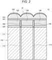
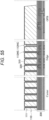
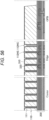
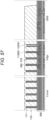
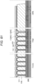
- Fig. 2 is a longitudinal cross-sectional view illustrating a cross-sectional configuration of the pixel unit 13.
- the pixel unit 13 includes a semiconductor substrate 110, an intermediate layer 120, a color filter 130, an insulating layer 141, an on-chip lens 151, and an antireflection film 152.
- the semiconductor substrate 110 is, for example, a substrate having a thickness of 1 ⁇ m to 6 ⁇ m and constituted by silicon (Si).
- the semiconductor substrate 110 is provided with a photoelectric conversion unit 111 that generates a signal charge corresponding to the amount of received incident light for each pixel 12.
- the photoelectric conversion unit 111 is, for example, a photodiode, and is configured by providing a semiconductor region of a second conductivity type (for example, N-type) inside a semiconductor region of a first conductivity type (for example, P-type) for each pixel 12.
- the photoelectric conversion units 111 provided for the respective pixels 12 are electrically separated from each other by a pixel separation wall 112 constituted by an insulating material.
- the pixel separation wall 112 may be constituted by, for example, an insulating material such as silicon oxide (SiO 2 ), silicon nitride (SiN), or silicon oxynitride (SiON), and may be provided to extend in the thickness direction of the semiconductor substrate 110.
- a circuit layer including a pixel circuit that converts the signal charge photoelectrically converted by the photoelectric conversion unit 111 into a pixel signal is provided on a surface (also referred to as a front surface) opposite to a surface (also referred to as a back surface) of the semiconductor substrate 110 on which the intermediate layer 120 is provided. That is, the imaging device 100 according to the present embodiment is a back-illuminated imaging device that receives light incident from the back surface of the semiconductor substrate 110.
- the intermediate layer 120 is a functional layer provided on the semiconductor substrate 110 with an insulating material.
- the intermediate layer 120 is provided on the semiconductor substrate 110 separately for each pixel 12 in a low refraction region 140 to be described later.
- the intermediate layer 120 may include a layer having a negative fixed charge.
- the intermediate layer 120 may include a layer constituted by a high dielectric material having a negative fixed charge such as hafnium oxide (HfO 2 ), zirconium oxide (ZrO 2 ), aluminum oxide (Al 2 O 3 ), tantalum oxide (Ta 2 O 5 ), titanium oxide (TiO 2 ), magnesium oxide (MgO), yttrium oxide (Y 2 O 3 ), or an oxide of a lanthanoid.
- HfO 2 hafnium oxide
- ZrO 2 zirconium oxide
- Al 2 O 3 aluminum oxide
- Ta 2 O 5 tantalum oxide
- magnesium oxide (MgO) magnesium oxide
- Y 2 O 3 yttrium oxide
- the intermediate layer 120 may include a layer having an antireflection function.
- the intermediate layer 120 may include a dielectric layer having a refractive index lower than that of the semiconductor substrate 110. In such a case, since the intermediate layer 120 can suppress reflection of light at the interface with the semiconductor substrate 110, it is possible to improve the incident efficiency of light on the photoelectric conversion unit 111.
- the intermediate layer 120 may be provided by sequentially stacking aluminum oxide (Al 2 O 3 ), tantalum oxide (Ta 2 O 5 ), and silicon oxide (SiO 2 ) from the semiconductor substrate 110 side.
- Al 2 O 3 aluminum oxide
- Ta 2 O 5 tantalum oxide
- SiO 2 silicon oxide
- the color filter 130 is provided for each pixel 12 on the intermediate layer 120, and selectively transmits light (for example, red light (R), green light (G), and blue light (B)) in a wavelength band corresponding to each pixel 12.
- the color filter 130 may be provided in a predetermined RGB array such as a Bayer array, for example.
- the color filter 130 is provided on the semiconductor substrate 110 separately for each pixel 12 in the low refraction region 140 to be described later.
- the color filter 130 may be provided, for example, by adding a pigment or dye to a transparent resin that transmits visible light.
- the color filter 130 may be a transparent filter constituted by a transparent resin that transmits visible light, an ND filter made by adding carbon black to a transparent resin, or the like.
- the color filter 130 and the intermediate layer 120 are separated for each pixel 12 by the low refraction region 140 extending in the thickness direction of the semiconductor substrate 110.
- the low refraction region 140 is a region having a refractive index lower than that of the color filter 130.
- the low refraction region 140 may be a region having a refractive index of 1.0 or more and 1.35 or less.
- the low refraction region 140 is provided between the color filters 130 provided for each pixel 12 and between the intermediate layers 120 provided for each pixel 12, so that the color filters 130 and the intermediate layers 120 can function as a waveguide in which a high refractive index material is sandwiched between low refractive index materials. According to this, since the low refraction region 140 can reflect the light traveling to the adjacent pixel 12 at the interface with the color filter 130 and the interface with the intermediate layer 120, the incident efficiency of the light on the photoelectric conversion unit 111 can be improved.
- the low refraction region 140 may be constituted by any material as long as the refractive index is lower than that of the color filter 130.
- the low refraction region 140 may be a gap, and may be constituted by an inorganic material such as silicon oxide (SiO 2 ), silicon nitride (SiN), or silicon oxynitride (SiON), or a resin material such as a styrene resin, an acrylic resin, a styrene-acrylic copolymer resin, or a siloxane resin.
- the low refraction region 140 may be constituted by a so-called low-k material such as SiOF, SiOC, or porous silica.
- the insulating layer 141 is constituted by an insulating material on the color filter 130.
- the insulating layer 141 is provided by forming a film of silicon oxide (SiO 2 ) or the like on the color filter 130. According to this, the insulating layer 141 formed with a high coverage on the color filter 130 separated for each pixel 12 seals the upper end while keeping the gap without burying the low refraction region 140 between the color filters 130, so that the low refraction region 140 can be configured as the gap.
- Fig. 3 is a longitudinal cross-sectional view illustrating a variation of the cross-sectional shape of the gap constituting the low refraction region 140.
- the cross-sectional shape of the gap constituting the low refraction region 140 may change depending on the covering situation of the inner wall of the low refraction region 140 by the insulating material that has entered the inside of the low refraction region 140 at the time of forming the insulating layer 141.
- the cross-sectional shape of the gap constituting the low refraction region 140 may be a spindle shape in which the upper end and the lower end are thinner than the central portion as illustrated in (A) of Fig. 3 .
- the cross-sectional shape of the gap constituting the low refraction region 140 may be a spindle shape in which the upper end is thinner than the central portion and the lower end is thicker than the central portion as illustrated in (B) of Fig. 3 .
- the cross-sectional shape of the gap constituting the low refraction region 140 may be a spindle shape in which the upper end is thicker than the central portion and the lower end is thinner than the central portion as illustrated in (C) of Fig. 3 .
- the cross-sectional shape of the gap constituting the low refraction region 140 may be a dumbbell shape in which the upper end is thicker than the central portion and the lower end is thicker than the central portion as illustrated in (D) of Fig. 3 .
- the on-chip lens 151 is provided for each pixel 12 on the insulating layer 141.
- the on-chip lens 151 may be constituted by, for example, a resin material such as a styrene resin, an acrylic resin, a styrene-acrylic copolymer resin, or a siloxane resin.
- the on-chip lens 151 condenses the light incident on the pixel 12, so that the light incident on the pixel 12 can be efficiently incident on the photoelectric conversion unit 111.
- the antireflection film 152 may be formed on the surface layer of the on-chip lens 151.
- the antireflection film 152 is configured as, for example, a dielectric multilayer film.
- the antireflection film 152 can suppress reflection of light incident on the on-chip lens 151.
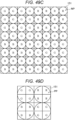
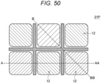
- Figs. 4A to 4C are plan views illustrating examples of planar configurations of the pixel unit 13.
- the low refraction region 140 may be provided over the entire circumference of the pixel 12 so as to surround each of the pixels 12 provided in the two-dimensional array. In such a case, the low refraction region 140 can more reliably reflect the light transmitted through the color filter 130 and the intermediate layer 120 and traveling to the adjacent pixel 12, so that color mixing with the adjacent pixel 12 can be more reliably suppressed.
- the low refraction region 140 may be provided in a region corresponding to each side of the pixels 12 provided in the two-dimensional array. Even in such a case, the low refraction region 140 can reflect most of the light transmitted through the color filter 130 and the intermediate layer 120 and traveling to the adjacent pixel 12, so that color mixing with the adjacent pixel 12 can be suppressed.
- each of pixels 12 may be provided so as to protrude in a rectangular shape with respect to the diagonal region 12A, so that the intervals between the pixels 12 may be substantially the same in both the diagonal region 12A and the region corresponding to the side of the pixel 12. According to this, the imaging device 100 can further simplify the process conditions of the manufacturing process of the pixel unit 13.
- the diagonal region 12A of each of the pixels 12 may be embedded with an inorganic material having a refractive index lower than that of the color filter 130, such as silicon oxide (SiO 2 ), silicon nitride (SiN), or silicon oxynitride (SiON), a resin material such as a styrene resin, an acrylic resin, a styrene-acrylic copolymer resin, or a siloxane resin, or a low-k material such as SiOF, SiOC, or porous silica.
- an inorganic material having a refractive index lower than that of the color filter 130 such as silicon oxide (SiO 2 ), silicon nitride (SiN), or silicon oxynitride (SiON), a resin material such as a styrene resin, an acrylic resin, a styrene-acrylic copolymer resin, or a siloxane resin, or a low-k material such as SiO
- the light transmitted through the color filter 130 and the intermediate layer 120 and traveling to the adjacent pixel 12 can be reflected by the material having the refractive index lower than that of the color filter 130, so that color mixing with the adjacent pixel 12 can be more reliably suppressed.
- Fig. 5 is a longitudinal cross-sectional view illustrating a cross-sectional configuration of a pixel unit 13A according to a first modification.
- the pixel unit 13A according to the first modification is different from the pixel unit 13 illustrated in Fig. 2 in that the low refraction region 140 is provided to extend from between the color filters 130 and between the intermediate layers 120 to the inside of the pixel separation wall 112.
- the low refraction region 140 is provided to extend from between the color filters 130 to the inside of the pixel separation wall 112 near the surface of the semiconductor substrate 110.
- the pixel unit 13A according to the first modification can suppress leakage of light between the photoelectric conversion units 111 of the adjacent pixels 12 in the low refraction region 140. Therefore, the pixel unit 13A according to the first modification can further suppress color mixing between the adjacent pixels 12.
- Fig. 6 is a longitudinal cross-sectional view illustrating a cross-sectional configuration of a pixel unit 13B according to a second modification.
- the pixel unit 13B according to the second modification is different from the pixel unit 13A illustrated in Fig. 5 in that the low refraction region 140 is provided to extend from between the color filters 130 and between the intermediate layers 120 to the on-chip lens 151 side.
- the low refraction region 140 is provided so as to extend from between the color filters 130 to the inside of the pixel separation wall 112 near the surface of the semiconductor substrate 110 and to extend to the on-chip lens 151 side to separate the on-chip lens 151 for each pixel 12.
- the pixel unit 13B according to the second modification can suppress leakage of light between the photoelectric conversion units 111 of the adjacent pixels 12 in the low refraction region 140. Furthermore, the pixel unit 13B according to the second modification can suppress leakage of light between the on-chip lenses 151 of the adjacent pixels 12 in the low refraction region 140. Therefore, the pixel unit 13B according to the second modification can further suppress color mixing between the adjacent pixels 12.
- Fig. 7 is a longitudinal cross-sectional view illustrating a cross-sectional configuration of a pixel unit 13C according to a third modification.
- the pixel unit 13C according to the third modification is different from the pixel unit 13 illustrated in Fig. 2 in that the low refraction region 140 is provided to extend from between the color filters 130 and between the intermediate layers 120 to the inside of the pixel separation wall 112.
- the low refraction region 140 is provided to extend from between the color filters 130 to the inside of the pixel separation wall 112 in the middle of the semiconductor substrate 110.
- the pixel unit 13C according to the third modification can suppress leakage of light between the photoelectric conversion units 111 of the adjacent pixels 12 in the low refraction region 140. Therefore, the pixel unit 13C according to the third modification can further suppress color mixing between the adjacent pixels 12.
- Fig. 8 is a longitudinal cross-sectional view illustrating a cross-sectional configuration of a pixel unit 13D according to a fourth modification.
- the pixel unit 13D according to the fourth modification is different from the pixel unit 13C illustrated in Fig. 7 in that the low refraction region 140 is provided to extend from between the color filters 130 and between the intermediate layers 120 to the on-chip lens 151 side.
- the low refraction region 140 extends from between the color filters 130 to the inside of the pixel separation wall 112 in the middle of the semiconductor substrate 110 and extends to the on-chip lens 151 side, and is provided to separate the on-chip lens 151 for each pixel 12.
- the pixel unit 13D according to the fourth modification can suppress leakage of light between the photoelectric conversion units 111 of the adjacent pixels 12 in the low refraction region 140. Furthermore, the pixel unit 13D according to the fourth modification can suppress leakage of light between the on-chip lenses 151 of the adjacent pixels 12 in the low refraction region 140. Therefore, the pixel unit 13D according to the fourth modification can further suppress color mixing between the adjacent pixels 12.
- Fig. 9 is a longitudinal cross-sectional view illustrating a cross-sectional configuration of a pixel unit 13E according to a fifth modification.
- the pixel unit 13E according to the fifth modification is different from the pixel unit 13 illustrated in Fig. 2 in that the low refraction region 140 is provided to extend from between the color filters 130 and between the intermediate layers 120 to the on-chip lens 151 side.
- the low refraction region 140 is provided so as to extend to the on-chip lens 151 side and separate the on-chip lens 151 for each pixel 12.
- the pixel unit 13E according to the fifth modification can suppress leakage of light between the on-chip lenses 151 of the adjacent pixels 12 in the low refraction region 140. Therefore, the pixel unit 13E according to the fifth modification can further suppress color mixing between the adjacent pixels 12.
- Fig. 10 is a longitudinal cross-sectional view illustrating a cross-sectional configuration of a pixel unit 13F according to a sixth modification.
- the pixel unit 13F according to the sixth modification is different from the pixel unit 13 illustrated in Fig. 2 in that the low refraction region 140 is provided to extend from between the color filters 130 and between the intermediate layers 120 to the inside of the pixel separation wall 112.
- the pixel separation wall 112 is provided to extend to the middle of the semiconductor substrate 110 in the thickness direction of the semiconductor substrate 110. Furthermore, the low refraction region 140 is provided to extend from between the color filters 130 to the inside of the pixel separation wall 112 in the middle of the semiconductor substrate 110.
- the pixel unit 13F according to the sixth modification can suppress leakage of light between the photoelectric conversion units 111 of the adjacent pixels 12 in the low refraction region 140. Therefore, the pixel unit 13F according to the seventh modification can further suppress color mixing between the adjacent pixels 12.
- Fig. 11 is a longitudinal cross-sectional view illustrating a cross-sectional configuration of a pixel unit 13G according to a seventh modification.
- the pixel unit 13G according to the seventh modification is different from the pixel unit 13F illustrated in Fig. 10 in that the low refraction region 140 is provided to extend from between the color filters 130 and between the intermediate layers 120 to the on-chip lens 151 side.
- the low refraction region 140 is provided to extend from between the color filters 130 to the inside of the pixel separation wall 112 in the middle of the semiconductor substrate 110, and is provided to extend to the on-chip lens 151 side to separate the on-chip lens 151 for each pixel 12.
- the pixel unit 13G according to the seventh modification can suppress leakage of light between the photoelectric conversion units 111 of the adjacent pixels 12 in the low refraction region 140. Furthermore, the pixel unit 13G according to the seventh modification can suppress leakage of light between the on-chip lenses 151 of the adjacent pixels 12 in the low refraction region 140. Therefore, the pixel unit 13G according to the seventh modification can further suppress color mixing between the adjacent pixels 12.
- Fig. 12 is a longitudinal cross-sectional view illustrating a cross-sectional configuration of a pixel unit 13H according to an eighth modification.
- the pixel unit 13H according to the eighth modification is different from the pixel unit 13 illustrated in Fig. 2 in that the pixel separation wall 112 is provided to extend to the middle of the semiconductor substrate 110 in the thickness direction of the semiconductor substrate 110.
- the pixel separation wall 112 can electrically separate the photoelectric conversion units 111 of the adjacent pixels 12. Therefore, even in the pixel unit 13H according to the eighth modification, color mixing between the adjacent pixels 12 can be suppressed, similarly to the pixel unit 13 illustrated in Fig. 2 .
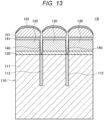
- Fig. 13 is a longitudinal cross-sectional view illustrating a cross-sectional configuration of a pixel unit 131 according to a ninth modification.
- the pixel unit 131 according to the ninth modification is different from the pixel unit 13H illustrated in Fig. 12 in that the low refraction region 140 is provided to extend from between the color filters 130 and between the intermediate layers 120 to the on-chip lens 151 side.
- the low refraction region 140 is provided so as to extend to the on-chip lens 151 side and separate the on-chip lens 151 for each pixel 12.
- the pixel unit 131 according to the ninth modification can suppress leakage of light between the on-chip lenses 151 of the adjacent pixels 12 in the low refraction region 140. Therefore, the pixel unit 131 according to the ninth modification can further suppress color mixing between the adjacent pixels 12.
- Fig. 14 is a longitudinal cross-sectional view illustrating a cross-sectional configuration of a pixel unit 13J according to a 10th modification.
- the pixel unit 13J according to the 10th modification is different from the pixel unit 13 illustrated in Fig. 2 in that a light shielding unit 113 is provided inside the pixel separation wall 112.
- the light shielding unit 113 is provided so as to be embedded inside the pixel separation wall 112 on the intermediate layer 120 side.
- the light shielding unit 113 may be constituted by a conductive material such as tungsten (W), aluminum (Al), copper (Cu), titanium nitride (TiN), or polysilicon (poly-Si) capable of shielding light.
- the light shielding unit 113 may be constituted by an organic resin material containing a carbon black pigment or a titanium black pigment.
- the light shielding unit 113 shields light leaking into the adjacent pixels 12 by the photoelectric conversion unit 111 in the vicinity of the intermediate layer 120, so that color mixing between the adjacent pixels 12 can be further suppressed. According to this, the pixel unit 13J according to the 10th modification can further suppress color mixing between the adjacent pixels 12.
- Fig. 15 is a longitudinal cross-sectional view illustrating a cross-sectional configuration of a pixel unit 13K according to an 11th modification.
- the pixel unit 13K according to the 11th modification is different from the pixel unit 13J illustrated in Fig. 14 in that the low refraction region 140 is provided to extend from between the color filters 130 and between the intermediate layers 120 to the on-chip lens 151 side.
- the low refraction region 140 is provided so as to extend to the on-chip lens 151 side and separate the on-chip lens 151 for each pixel 12.
- the pixel unit 13K according to the 11th modification can suppress leakage of light between the on-chip lenses 151 of the adjacent pixels 12 in the low refraction region 140. Therefore, the pixel unit 13K according to the 11th modification can further suppress color mixing between the adjacent pixels 12.
- Fig. 16 is a longitudinal cross-sectional view illustrating a cross-sectional configuration of a pixel unit 13L according to a 12th modification.
- the pixel unit 13L according to the 12th modification is different from the pixel unit 13J illustrated in Fig. 14 in that the pixel separation wall 112 is provided to extend to the middle of the semiconductor substrate 110 in the thickness direction of the semiconductor substrate 110.
- the pixel separation wall 112 can electrically separate the photoelectric conversion units 111 of the adjacent pixels 12. Therefore, even in the pixel unit 13L according to the 12th modification, color mixing between the adjacent pixels 12 can be suppressed, similarly to the pixel unit 13J illustrated in Fig. 14 .
- Fig. 17 is a longitudinal cross-sectional view illustrating a cross-sectional configuration of a pixel unit 13M according to a 13th modification.
- the pixel unit 13M according to the 13th modification is different from the pixel unit 13L illustrated in Fig. 16 in that the low refraction region 140 is provided to extend from between the color filters 130 and between the intermediate layers 120 to the on-chip lens 151 side.
- the low refraction region 140 is provided so as to extend to the on-chip lens 151 side and separate the on-chip lens 151 for each pixel 12.
- the pixel unit 13M according to the 13th modification can suppress leakage of light between the on-chip lenses 151 of the adjacent pixels 12 in the low refraction region 140. Therefore, the pixel unit 13M according to the 13th modification can further suppress color mixing between the adjacent pixels 12.
- Fig. 18 is a longitudinal cross-sectional view illustrating a cross-sectional configuration of a pixel unit 13N according to a 14th modification.
- the pixel unit 13N according to the 14th modification is different from the pixel unit 13J illustrated in Fig. 14 in that the light shielding unit 113 is provided so as to extend inside the pixel separation wall 112 and penetrate the semiconductor substrate 110.
- the pixel unit 13N according to the 14th modification can shield light leaking into the photoelectric conversion units 111 of the adjacent pixels 12 by the light shielding unit 113 over the entire pixel separation wall 112, color mixing between the adjacent pixels 12 can be further suppressed.
- Fig. 19 is a longitudinal cross-sectional view illustrating a cross-sectional configuration of a pixel unit 13O according to a 15th modification.
- the pixel unit 13O according to the 15th modification is different from the pixel unit 13N illustrated in Fig. 18 in that the low refraction region 140 is provided to extend from between the color filters 130 and between the intermediate layers 120 to the on-chip lens 151 side.
- the low refraction region 140 is provided so as to extend to the on-chip lens 151 side and separate the on-chip lens 151 for each pixel 12.
- the pixel unit 13O according to the 15th modification leakage of light between the on-chip lenses 151 of the adjacent pixels 12 can be suppressed in the low refraction region 140. Therefore, the pixel unit 13O according to the 15th modification can further suppress color mixing between the adjacent pixels 12.
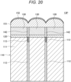
- Fig. 20 is a longitudinal cross-sectional view illustrating a cross-sectional configuration of a pixel unit 13P according to a 16th modification.
- the pixel unit 13P according to the 16th modification is different from the pixel unit 13J illustrated in Fig. 14 in that the low refraction region 140 is provided as a low refraction layer 142 instead of a gap.
- the low refraction layer 142 is constituted by a material having a refractive index lower than that of the color filter 130, and is provided between the color filters 130 provided for the respective pixels 12 and between the intermediate layers 120 provided for the respective pixels 12.
- the material having a refractive index lower than that of the color filter 130 is, for example, an inorganic material such as silicon oxide (SiO 2 ), silicon nitride (SiN), or silicon oxynitride (SiON), a resin material such as a styrene resin, an acrylic resin, a styrene-acrylic copolymer resin, or a siloxane resin, or a low-k material such as SiOF, SiOC, or porous silica.
- the low refraction layer 142 can cause the color filter 130 and the intermediate layer 120 to function as a waveguide in which a high refractive index material is sandwiched between low refractive index materials.
- the pixel unit 13P according to the 16th modification can reflect light traveling to the adjacent pixel 12 at the interface between the low refraction layer 142 and the color filter 130 and the interface between the low refraction layer 142 and the intermediate layer 120. Therefore, even in the pixel unit 13P according to the 16th modification, color mixing between the adjacent pixels 12 can be suppressed, similarly to the pixel unit 13J illustrated in Fig. 14 .
- Fig. 21 is a longitudinal cross-sectional view illustrating a cross-sectional configuration of a pixel unit 13Q according to a 17th modification.
- the pixel unit 13Q according to the 17th modification is different from the pixel unit 13J illustrated in Fig. 14 in that an antireflection layer 153 is provided between the insulating layer 141 and the on-chip lens 151, and an antireflection intermediate layer 121 is provided instead of the intermediate layer 120.
- the antireflection intermediate layer 121 and the antireflection layer 153 include, for example, a dielectric multilayer film.
- the antireflection intermediate layer 121 and the antireflection layer 153 suppress reflection of incident light at an interface between layers existing from the on-chip lens 151 to the semiconductor substrate 110, so that it is possible to improve light incident efficiency on the photoelectric conversion unit 111.
- the antireflection intermediate layer 121 and the antireflection layer 153 may be provided in a configuration other than the dielectric multilayer film as long as they have an antireflection function.
- the antireflection intermediate layer 121 and the antireflection layer 153 may be provided as layers having a motheye structure.
- the pixel unit 13Q according to the 17th modification can further improve the incident efficiency of light on the photoelectric conversion unit 111 by further suppressing reflection of incident light.
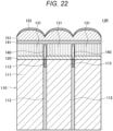
- Fig. 22 is a longitudinal cross-sectional view illustrating a cross-sectional configuration of a pixel unit 13R according to an 18th modification. As illustrated in Fig. 22 , the pixel unit 13R according to the 18th modification is different from the pixel unit 13J illustrated in Fig. 14 in that an inorganic color filter 131 is provided instead of the color filter 130.
- the inorganic color filter 131 is a filter that selectively transmits light (for example, red light, green light, and blue light) in a predetermined wavelength band by a structure of a dielectric laminated film, a photonic crystal, a quantum dot, a metamaterial, or the like, instead of a pigment or a dye.
- the inorganic color filter 131 is less likely to be discolored by ultraviolet rays, heat, or the like than a pigment or a dye. Therefore, the pixel unit 13R according to the 18th modification can suppress color mixing between adjacent pixels 12, similarly to the pixel unit 13J illustrated in Fig. 14 , even under a more severe environment.
- Fig. 23 is a longitudinal cross-sectional view illustrating a cross-sectional configuration of a pixel unit 13S according to a 19th modification.
- the pixel unit 13S according to the 19th modification is different from the pixel unit 13J illustrated in Fig. 14 in that a low refraction region 140A is further provided in a portion where the light shielding unit 113 is not provided in the pixel separation wall 112.
- the low refraction region 140A is a region having a refractive index lower than that of the pixel separation wall 112.
- the low refraction region 140A can reflect light leaking into the photoelectric conversion unit 111 of the adjacent pixel 12 by being provided to extend inside the pixel separation wall 112 in a portion where the light shielding unit 113 is not provided.
- the low refraction region 140A may be a gap, and may be constituted by an inorganic material such as silicon oxide (SiO 2 ), silicon nitride (SiN), or silicon oxynitride (SiON), a resin material such as a styrene resin, an acrylic resin, a styrene-acrylic copolymer resin, or a siloxane resin, or a low-k material such as SiOF, SiOC, or porous silica.
- an inorganic material such as silicon oxide (SiO 2 ), silicon nitride (SiN), or silicon oxynitride (SiON), a resin material such as a styrene resin, an acrylic resin, a styrene-acrylic copolymer resin, or a siloxane resin, or a low-k material such as SiOF, SiOC, or porous silica.
- the pixel unit 13S according to the 19th modification can shield or reflect light leaking into the photoelectric conversion unit 111 of the adjacent pixel 12 over the entire pixel separation wall 112, color mixing between the adjacent pixels 12 can be further suppressed.
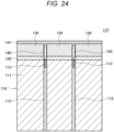
- Fig. 24 is a longitudinal cross-sectional view illustrating a cross-sectional configuration of a pixel unit 13T according to a 20th modification. As illustrated in Fig. 24 , the pixel unit 13T according to the 20th modification is different from the pixel unit 13J illustrated in Fig. 14 in that the on-chip lens 151 is not provided.
- Fig. 25 is a longitudinal cross-sectional view illustrating a cross-sectional configuration of a pixel unit 13U according to a 21st modification. As illustrated in Fig. 25 , the pixel unit 13U according to the 21st modification is different from the pixel unit 13J illustrated in Fig. 14 in that a phase difference lens 161 is provided instead of the on-chip lens 151.
- the phase difference lens 161 is a lens that exhibits a light condensing function by using a phase difference of incident light due to a metamaterial structure. Note that an antireflection layer 162 may be provided on the light incident surface of the phase difference lens 161.
- the phase difference lens 161 is used instead of the on-chip lens 151 that is a hemispherical convex lens, incident light can be condensed for each pixel 12. Therefore, even in the pixel unit 13T according to the 21st modification, color mixing between the adjacent pixels 12 can be suppressed, similarly to the pixel unit 13J illustrated in Fig. 14 .
- Fig. 26 is a longitudinal cross-sectional view illustrating a cross-sectional configuration of a pixel unit 13V according to a 22nd modification. As illustrated in Fig. 26 , the pixel unit 13V according to the 22nd modification is different from the pixel unit 13J illustrated in Fig. 14 in that a normal pixel NP and a phase difference pixel PP are mixed.
- the phase difference pixel PP includes a plurality of subpixels SP and one on-chip lens 151 provided on the plurality of subpixels SP.
- the phase difference pixel PP can detect the distance to the subject on the basis of the pixel signal obtained in each of the plurality of subpixels SP.
- the low refraction region 140 is not provided between the subpixels SP, but is provided between the phase difference pixel PP and the normal pixel NP. Even in a case where the pixel unit 13V according to the 22nd modification includes the normal pixel NP and the phase difference pixel PP, it is possible to suppress color mixing between the phase difference pixel PP and the normal pixel NP or between the normal pixels NP similarly to the pixel unit 13J illustrated in Fig. 14 .
- the on-chip lens 151 provided in the phase difference pixel PP is provided so as to be higher in height than the on-chip lens 151 provided in the normal pixel NP. According to this, the on-chip lens 151 provided in the phase difference pixel PP can control the focal position on the side of the on-chip lens 151 so that the separation ratio in the subpixel SP is improved. Therefore, the pixel unit 13V according to the 22nd modification can improve the phase difference amount of the phase difference pixel PP.
- Fig. 27 is a longitudinal cross-sectional view illustrating a cross-sectional configuration of a pixel unit 13W according to a 23rd modification.
- the pixel unit 13W according to the 23rd modification is different from the pixel unit 13J illustrated in Fig. 14 in that the normal pixel NP and the phase difference pixel PP are mixed. Since the normal pixel NP and the phase difference pixel PP have been described in the pixel unit 13V according to the 22nd modification, the description thereof is omitted here.
- the low refraction layer 142 having a width larger than that of the low refraction region 140 provided between the normal pixels NP is provided between the phase difference pixel PP and the normal pixel NP.
- the phase difference pixel PP can control the focus on the side of the on-chip lens 151 such that the separation ratio in the subpixel SP is improved by the waveguide effect by the low refraction layer 142. Therefore, the pixel unit 13W according to the 23rd modification can improve the phase difference amount of the phase difference pixel PP.
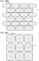
- Figs. 28A to 28C are plan views illustrating examples of planar arrangements in a case where the phase difference pixel PP and the normal pixel NP are mixed.
- Figs. 29A to 29C are plan views illustrating examples of planar arrangements in a case of only the phase difference pixels PP.
- the phase difference pixel PP may be provided in a size of 2p ⁇ 1p in a case where the pixel pitch of the normal pixel NP is p.
- the phase difference pixel PP can include two subpixels SP.
- the phase difference pixel PP may be provided alone among the normal pixels NP as illustrated in Fig. 28A , or a plurality of phase difference pixels PP may be provided side by side among the normal pixels NP as illustrated in Fig. 28B . Furthermore, the phase difference pixel PP may be provided in a region in which only the phase difference pixels PP are arranged as illustrated in Figs. 29A and 29B . In such a case, the phase difference pixels PP may be arranged in a matrix as illustrated in Fig. 29A , or may be alternately arranged as illustrated in Fig. 29B .
- the phase difference pixels PP may be provided with a size of 2p ⁇ 2p in a case where the pixel pitch of the normal pixels NP is p.
- the phase difference pixel PP can include four subpixels SP.
- the phase difference pixel PP may be provided alone among the normal pixels NP as illustrated in Fig. 28C . Furthermore, the phase difference pixel PP may be provided in a region in which only the phase difference pixels PP are arranged as illustrated in Fig. 29C . In such a case, the phase difference pixels PP may be arranged in a matrix as illustrated in Fig. 29C .
- Fig. 30 is a longitudinal cross-sectional view illustrating a cross-sectional configuration of the pixel unit 21.
- the pixel unit 21 includes the semiconductor substrate 110, the intermediate layer 120, the color filter 130, the insulating layer 141, the on-chip lens 151, and the antireflection film 152.
- the semiconductor substrate 110 is, for example, a substrate having a thickness of 1 ⁇ m to 6 ⁇ m and constituted by silicon (Si).
- the semiconductor substrate 110 is provided with a photoelectric conversion unit 111 that generates a signal charge corresponding to the amount of received incident light for each pixel 12.
- the photoelectric conversion unit 111 is, for example, a photodiode, and is configured by providing a semiconductor region of a second conductivity type (for example, N-type) inside a semiconductor region of a first conductivity type (for example, P-type) for each pixel 12.
- the photoelectric conversion units 111 provided for the respective pixels 12 are electrically separated from each other by a pixel separation wall 112 constituted by an insulating material.
- the pixel separation wall 112 may be constituted by, for example, an insulating material such as silicon oxide (SiO 2 ), silicon nitride (SiN), or silicon oxynitride (SiON), and may be provided to extend in the thickness direction of the semiconductor substrate 110.
- the pixel separation wall 112 is provided with the light shielding unit 113.
- the light shielding unit 113 is provided on the intermediate layer 120 side of the pixel separation wall 112.
- the light shielding unit 113 may be constituted by a conductive material such as tungsten (W), aluminum (Al), copper (Cu), titanium nitride (TiN), or polysilicon (poly-Si) capable of shielding light, or may be constituted by an organic resin material containing a carbon black pigment or a titanium black pigment.
- the light shielding unit 113 shields light leaking into the adjacent pixels 12, thereby further suppressing color mixing between the adjacent pixels 12.
- the intermediate layer 120 is a functional layer provided on the semiconductor substrate 110 with an insulating material.
- the intermediate layer 120 is provided on the semiconductor substrate 110 separately for each pixel 12 in the low refraction region 140.
- the intermediate layer 120 is configured by sequentially stacking a fixed charge layer 124, a reflection control layer 123, and a dielectric layer 122 from the semiconductor substrate 110 side.
- the dielectric layer 122 is a layer constituted by a dielectric material and extending from the pixel separation wall 112 along the bottom surface and the side surface of the light shielding unit 113 and the lower surface of the color filter 130. Specifically, the dielectric layer 122 is provided to extend from the pixel separation wall 112 so as to surround the lower surface and the side surface of the light shielding unit 113 provided on the intermediate layer 120 side of the pixel separation wall 112. The dielectric layer 122 further extends above the semiconductor substrate 110 and is provided along the lower surface of the color filter 130.
- the dielectric layer 122 is constituted by the same insulating material (that is, the dielectric material) as the pixel separation wall 112, and may be formed in the same process as the pixel separation wall 112.
- the pixel separation wall 112 and the dielectric layer 122 may be configured by depositing silicon oxide (SiO 2 ), silicon nitride (SiN), silicon oxynitride (SiON), or the like using atomic layer deposition (ALD).
- the thickness of the dielectric layer 122 provided along the side surface of the light shielding unit 113 is at least substantially the same as the thickness of the dielectric layer 122 provided along the lower surface of the light shielding unit 113.
- the thickness of the dielectric layer 122 provided along the lower surface of the color filter 130 may be substantially the same as the thickness of the dielectric layer 122 provided along the side surface and the lower surface of the light shielding unit 113.
- the thickness of the dielectric layer 122 provided along the side surface of the light shielding unit 113 may be thinner than the thickness of the dielectric layer 122 provided along the lower surface of the light shielding unit 113.
- the pixel unit 21 can further improve characteristics such as color mixing suppression and quantum efficiency of the pixel 12.
- the fixed charge layer 124 is constituted by a material having a negative fixed charge, and is provided between the dielectric layer 122 and the semiconductor substrate 110.
- the fixed charge layer 124 may be constituted by a high dielectric material having a negative fixed charge such as hafnium oxide (HfO 2 ), zirconium oxide (ZrO 2 ), aluminum oxide (Al 2 O 3 ), tantalum oxide (Ta 2 O 5 ), titanium oxide (TiO 2 ), magnesium oxide (MgO), yttrium oxide (Y 2 O 3 ), or an oxide of a lanthanoid. Since the fixed charge layer 124 can form a region in which positive charges are accumulated in the interface region with the semiconductor substrate 110 by negative fixed charges, generation of dark current between the dielectric layer 122 and the semiconductor substrate 110 can be suppressed.
- the fixed charge layer 124 may be provided to extend between the semiconductor substrate 110 and the dielectric layer 122 provided on the side surface of the light shielding unit 113 and the pixel separation wall 112 continuous with the dielectric layer 122.
- the fixed charge layer 124 may be provided so as to be interposed between the semiconductor substrate 110 and the dielectric layer 122 and the pixel separation wall 112 constituted by an insulating material (that is, the dielectric material).
- the fixed charge layer 124 can suppress generation of a dark current between the dielectric layer 122 and the pixel separation wall 112 and the semiconductor substrate 110 due to a negative fixed charge.
- the reflection control layer 123 is constituted by a material having a refractive index higher than the refractive index of the dielectric layer 122 and lower than the refractive index of the semiconductor substrate 110, and is provided between the fixed charge layer 124 and the dielectric layer 122.
- the reflection control layer 123 may be provided between the fixed charge layer 124 provided on the surface of the semiconductor substrate 110 and the dielectric layer 122 provided on the lower surface of the color filter 130. Since the reflection control layer 123 can suppress reflection of light at the interface with the dielectric layer 122 or the interface with the semiconductor substrate 110, it is possible to improve the incident efficiency of light on the photoelectric conversion unit 111.
- the color filter 130 is provided for each pixel 12 on the intermediate layer 120, and selectively transmits light (for example, red light (R), green light (G), and blue light (B)) in a wavelength band corresponding to each pixel 12.
- the color filter 130 may be provided in a predetermined RGB array such as a Bayer array, for example.
- the color filter 130 may be provided by adding a pigment or dye to a transparent resin that transmits visible light.
- the color filter 130 may include a transparent filter constituted by a transparent resin that transmits visible light, an ND filter obtained by adding carbon black to a transparent resin, or the like.
- the color filter 130 and the intermediate layer 120 are separated for each pixel 12 by the low refraction region 140 extending in the thickness direction of the semiconductor substrate 110.
- the low refraction region 140 only needs to separate at least one layer of the dielectric layer 122, the reflection control layer 123, and the fixed charge layer 124 included in the intermediate layer 120 for each pixel 12.
- the low refraction region 140 is a region having a refractive index lower than that of the color filter 130.
- the low refraction region 140 may be a region having a refractive index of 1.0 or more and 1.35 or less.
- the low refraction region 140 is provided between the color filters 130 provided for each pixel 12 and between the intermediate layers 120 provided for each pixel 12.
- the low refraction region 140 can cause the color filter 130 and the intermediate layer 120 to function as a waveguide in which the high refractive index material is sandwiched between the low refractive index materials. Therefore, since the low refraction region 140 can reflect the light traveling to the adjacent pixel 12 at the interface with the color filter 130 and the interface with the intermediate layer 120, the incident efficiency of the light on the photoelectric conversion unit 111 can be improved.
- the low refraction region 140 may be constituted by any material as long as the refractive index is lower than that of the color filter 130.
- the low refraction region 140 may be a gap, and may be constituted by an inorganic material such as silicon oxide (SiO 2 ), silicon nitride (SiN), or silicon oxynitride (SiON), or a resin material such as a styrene resin, an acrylic resin, a styrene-acrylic copolymer resin, or a siloxane resin.
- the low refraction region 140 may be constituted by a so-called low-k material such as SiOF, SiOC, or porous silica.
- the insulating layer 141 is constituted by an insulating material on the color filter 130.
- the insulating layer 141 is provided by forming a film of silicon oxide (SiO 2 ) or the like on the color filter 130. According to this, the insulating layer 141 is formed with a high coverage on the color filter 130 separated for each pixel 12, so that the upper end can be sealed without being embedded while the low refraction region 140 between the color filters 130 is kept as a gap.
- the on-chip lens 151 is provided for each pixel 12 on the insulating layer 141.
- the on-chip lens 151 may be constituted by, for example, a resin material such as a styrene resin, an acrylic resin, a styrene-acrylic copolymer resin, or a siloxane resin.
- the on-chip lens 151 condenses the light incident on the pixel 12, so that the light incident on the pixel 12 can be efficiently incident on the photoelectric conversion unit 111.
- the antireflection film 152 may be formed on the surface layer of the on-chip lens 151.
- the antireflection film 152 is configured as, for example, a dielectric multilayer film.
- the antireflection film 152 can suppress reflection of light incident on the on-chip lens 151.
- Fig. 31 is an enlarged longitudinal cross-sectional view of the vicinity of the light shielding unit 113 in Fig. 30 .
- the thickness of the dielectric layer 122 provided along the lower surface of the light shielding unit 113 is t1
- the thickness of the dielectric layer 122 provided along the side surface of the light shielding unit 113 is t2
- the thickness of the dielectric layer 122 provided along the lower surface of the color filter 130 is t3.
- Such a dielectric layer 122 can be formed by using atomic layer deposition (ALD) capable of depositing a highly accurate and uniform film on an arbitrary structure.
- ALD atomic layer deposition
- the dielectric layer 122 may be provided such that t2 is smaller than t1 or t3. Since the thickness of the dielectric layer 122 provided along the side surface of the light shielding unit 113 becomes thinner, the pixel unit 21 can suppress color mixing between adjacent pixels 12 and can further enhance the quantum efficiency of the photoelectric conversion unit 111.
- the sum of the thickness of the dielectric layer 122 provided along both side surfaces of the light shielding unit 113 and the width of the light shielding unit 113 is W1, and the width of the pixel separation wall 112 is w2.
- the dielectric layer 122 and the pixel separation wall 112 may be provided so as to satisfy W1 > W2. Since the light shielding unit 113 is provided with a width that makes the total width of the light shielding unit 113 and the dielectric layer 122 larger than the width of the pixel separation wall 112, color mixing between adjacent pixels 12 can be further suppressed.
- the width of the light shielding unit 113 is W3, and the width of the low refraction region 140 is W4.
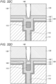
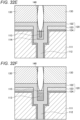
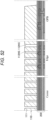
- Figs. 32A to 32F are longitudinal cross-sectional views illustrating variations of the configuration in the vicinity of the light shielding unit 113. As illustrated in Figs. 32A to 32F , in the pixel unit 21 according to the first modification, variations may be added to the configuration in the vicinity of the light shielding unit 113.
- the light shielding unit 113 may be provided such that the width W3 of the light shielding unit 113 is wider than the width W4 of the low refraction region 140. By providing the light shielding unit 113 with a wider width, color mixing between the adjacent pixels 12 can be further suppressed.
- the light shielding unit 113 may be provided to extend to the upper side along the inner surface of the opening in which the low refraction region 140 is provided.
- the light shielding unit 113 may be provided to extend to the upper side along the inner surface of the concave structure by attaching a conductive material to the inner surface of the concave structure formed by the dielectric layer 122. Even in such a case, the light shielding unit 113 can suppress color mixing between the adjacent pixels 12.
- the light shielding unit 113 and the low refraction region 140 may be provided so as not to be in contact with each other.
- the dielectric layer 122 may be provided between the light shielding unit 113 and the low refraction region 140. In such a case, since the dielectric layer 122 can protect the light shielding unit 113 from the influence that may occur in the process of forming the low refraction region 140, characteristic deterioration of the light shielding unit 113 can be prevented.
- a low refraction layer 143 constituted by an insulating material having a refractive index lower than that of the dielectric layer 122 may be provided between the light shielding unit 113 and the low refraction region 140.
- the low refraction layer 143 can protect the light shielding unit 113 from the influence that may occur in the process of forming the low refraction region 140, characteristic deterioration of the light shielding unit 113 can be suppressed.
- the low refraction layer 143 can form the waveguide having the high refractive index material sandwiched between the low refractive index materials up to immediately above the light shielding unit 113, it is possible to improve the incident efficiency of light to the photoelectric conversion unit 111.
- a diffusion prevention layer 114 constituted by Ti, TiN, or the like may be provided between the light shielding unit 113 and the dielectric layer 122.
- the diffusion prevention layer 114 can prevent mutual diffusion of atoms between the dielectric layer 122 and the light shielding unit 113. Therefore, the diffusion prevention layer 114 can prevent characteristic deterioration of the dielectric layer 122 and the light shielding unit 113.
- a cap layer 115 constituted by Ti, TiN, or the like may be provided on the upper surface of the light shielding unit 113. Since the cap layer 115 can protect the light shielding unit 113 from the influence that may occur in the process of forming the low refraction region 140, characteristic deterioration of the light shielding unit 113 can be prevented. Furthermore, since the cap layer 115 constituted by Ti, TiN, or the like can shield light leaking into the adjacent pixels 12 similarly to the light shielding unit 113, it is also possible to suppress color mixing between the adjacent pixels 12.
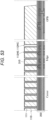
- Fig. 33 is a longitudinal cross-sectional view illustrating a cross-sectional configuration of a pixel unit 21A according to a second modification.
- the pixel unit 21A according to the second modification is different from the pixel unit 21 illustrated in Fig. 30 in that the light shielding unit 113 is provided in a reverse tapered shape.
- the light shielding unit 113 may be provided in a reverse tapered shape expanding toward the upper side where the color filter 130 and the low refraction region 140 are provided. Since the light shielding unit 113 having such a reverse tapered shape is easier to form than the light shielding unit 113 having a non-tapered shape, it is possible to reduce the difficulty in the manufacturing process of the pixel unit 21A.
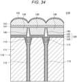
- Fig. 34 is a longitudinal cross-sectional view illustrating a cross-sectional configuration of a pixel unit 21B according to a third modification. As illustrated in Fig. 34 , the pixel unit 21B according to the third modification is different from the pixel unit 21A illustrated in Fig. 33 in that the low refraction region 140 is further provided in a tapered shape.
- the low refraction region 140 may be provided in a tapered shape that narrows toward the upper side where the on-chip lens 151 is provided.
- the upper end can be easily sealed with the insulating layer 141, so that the difficulty in the manufacturing process of the pixel unit 21A can be reduced.
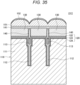
- Fig. 35 is a longitudinal cross-sectional view illustrating a cross-sectional configuration of a pixel unit 21C according to a fourth modification.
- the pixel unit 21C according to the fourth modification is different from the pixel unit 21 illustrated in Fig. 30 in that the pixel separation wall 112 is provided to extend to the middle of the semiconductor substrate 110 in the thickness direction of the semiconductor substrate 110.
- the pixel separation wall 112 is provided to extend to the middle of the semiconductor substrate 110, so that the photoelectric conversion units 111 of the adjacent pixels 12 can be electrically separated, similarly to the pixel unit 21 illustrated in Fig. 30 . Therefore, the pixel unit 21C according to the fourth modification can suppress color mixing between adjacent pixels 12, similarly to the pixel unit 21 illustrated in Fig. 30 .
- Fig. 36 is a longitudinal cross-sectional view illustrating a cross-sectional configuration of a pixel unit 21D according to a fifth modification. As illustrated in Fig. 36 , the pixel unit 21D according to the fifth modification is different from the pixel unit 21 illustrated in Fig. 30 in that the insulating layer 141 is not provided.
- the pixel unit 21D can form the low refraction region 140 by sealing the upper end of the gap with the on-chip lens 151. Furthermore, in a case where the low refraction region 140 includes a low refractive material having a refractive index lower than that of the color filter 130, the pixel unit 21D can form the low refraction region 140 by embedding the low refractive material between the color filters 130 and between the intermediate layers 120.
- the pixel unit 21D according to the fifth modification can appropriately form the low refraction region 140, and thus, it is possible to suppress color mixing between the adjacent pixels 12, similarly to the pixel unit 21 illustrated in Fig. 30 .
- Fig. 37 is a longitudinal cross-sectional view illustrating a cross-sectional configuration of a pixel unit 21E according to a sixth modification.
- the pixel unit 21E according to the sixth modification is different from the pixel unit 21 illustrated in Fig. 30 in that the low refraction layer 143 constituted by an insulating material having a refractive index lower than that of the dielectric layer 122 is provided between the light shielding unit 113 and the low refraction region 140.
- the low refraction layer 143 is constituted by an inorganic material having a refractive index lower than that of the dielectric layer 122, such as silicon oxide (SiO 2 ), silicon nitride (SiN), or silicon oxynitride (SiON), or a resin material such as a styrene resin, an acrylic resin, a styrene-acrylic copolymer resin, or a siloxane resin. Since the low refraction layer 143 can protect the light shielding unit 113 from the influence that may occur in the process of forming the low refraction region 140, characteristic deterioration of the light shielding unit 113 can be suppressed.
- an inorganic material having a refractive index lower than that of the dielectric layer 122 such as silicon oxide (SiO 2 ), silicon nitride (SiN), or silicon oxynitride (SiON), or a resin material such as a styrene resin, an acrylic resin,
- the low refraction layer 143 can form the waveguide having the high refractive index material sandwiched between the low refractive index materials up to immediately above the light shielding unit 113, it is possible to improve the incident efficiency of light to the photoelectric conversion unit 111.
- Fig. 38 is a longitudinal cross-sectional view illustrating a cross-sectional configuration of a pixel unit 21F according to a seventh modification.
- the pixel unit 21F according to the seventh modification is different from the pixel unit 21 illustrated in Fig. 30 in that the low refraction region 140 is provided not as a gap but as the low refraction layer 142.
- the low refraction layer 142 is constituted by a material having a refractive index lower than that of the color filter 130, and is provided between the color filters 130 provided for the respective pixels 12 and between the intermediate layers 120.
- the material having a refractive index lower than that of the color filter 130 is, for example, an inorganic material such as silicon oxide (SiO 2 ), silicon nitride (SiN), or silicon oxynitride (SiON), a resin material such as a styrene resin, an acrylic resin, a styrene-acrylic copolymer resin, or a siloxane resin, or a low-k material such as SiOF, SiOC, or porous silica.
- an inorganic material such as silicon oxide (SiO 2 ), silicon nitride (SiN), or silicon oxynitride (SiON)
- a resin material such as a styrene resin, an acrylic resin, a st
- the low refraction layer 142 can cause the color filter 130 and the intermediate layer 120 to function as a waveguide in which a high refractive index material is sandwiched between low refractive index materials.
- the pixel unit 21F according to the seventh modification can reflect light traveling to the adjacent pixel 12 at the interface between the low refraction layer 142 and the color filter 130 and the interface between the low refraction layer 142 and the intermediate layer 120. Therefore, the pixel unit 21F according to the seventh modification can suppress color mixing between adjacent pixels 12, similarly to the pixel unit 21 illustrated in Fig. 30 .
- Figs. 39 to 41 are longitudinal cross-sectional views illustrating cross-sectional configurations of pixel units 21G, 21H, and 211 according to an eighth modification.
- the pixel units 21G, 21H, and 211 according to the eighth modification are provided such that the configuration on the upper side (that is, the light incident surface side) of the semiconductor substrate 110 is shifted in the light incident direction in order to allow light having a large incident angle to be more efficiently incident on the photoelectric conversion unit 111.
- Such a shift is referred to as pupil correction or the like, and is performed, for example, in the pixel 12 provided in a region having a large incident angle of light, such as a peripheral edge of the pixel region.
- the low refraction region 140 is provided as the low refraction layer 142 instead of the gap.
- the pixel units 21G, 21H, and 21I can more easily shift the configuration on the upper side of the semiconductor substrate 110 as compared with a case where the low refraction region 140 is a gap.
- the on-chip lens 151 may be provided to be shifted in the light incident direction with respect to the color filter 130 and the low refraction layer 142.
- the on-chip lens 151, the color filter 130, and the low refraction layer 142 may be provided to be shifted in the incident direction of light with respect to the dielectric layer 122. Furthermore, the on-chip lens 151 may be further shifted in the light incident direction with respect to the color filter 130 and the low refraction layer 142.
- the on-chip lens 151, the color filter 130, the low refraction layer 142, and the dielectric layer 122 may be provided to be shifted in the incident direction of light with respect to the reflection control layer 123. Furthermore, the on-chip lens 151, the color filter 130, and the low refraction layer 142 may be provided to be shifted in the incident direction of light with respect to the dielectric layer 122, and the on-chip lens 151 may be provided to be further shifted in the incident direction of light with respect to the color filter 130 and the low refraction layer 142.
- the pixel units 21G, 21H, and 21I according to the eighth modification can cause light having a large incident angle to be incident on the photoelectric conversion unit 111 more efficiently. Therefore, the pixel units 21G, 21H, and 21I according to the eighth modification can cause light to be incident on the photoelectric conversion unit 111 more efficiently even in the pixel 12 at the peripheral edge of the pixel region.
- Fig. 42 is a longitudinal cross-sectional view illustrating a cross-sectional configuration of a pixel unit 21J according to a ninth modification. As illustrated in Fig. 42 , the pixel unit 21J according to the ninth modification is different from the pixel unit 21 illustrated in Fig. 30 in that the normal pixel NP and the phase difference pixel PP are mixed.
- the phase difference pixel PP includes a plurality of subpixels SP and one on-chip lens 151 provided on the plurality of subpixels SP.
- the phase difference pixel PP can detect the distance to the subject on the basis of the pixel signal obtained in each of the plurality of subpixels SP.
- the low refraction region 140 is not provided between the subpixels SP, but is provided between the phase difference pixel PP and the normal pixel NP.
- the pixel unit 21J according to the ninth modification can suppress color mixing between the phase difference pixel PP and the normal pixel NP or between the normal pixels NP.
- Fig. 43 is a longitudinal cross-sectional view illustrating a cross-sectional configuration of a pixel unit 21K according to a 10th modification. As illustrated in Fig. 43 , the pixel unit 21K according to the 10th modification is different from the pixel unit 21J illustrated in Fig. 42 in that each of the subpixels SP is not separated by the pixel separation wall 112.
- each of the subpixels SP is electrically separated from each other by a mode of introducing a conductivity type impurity into the semiconductor substrate 110.
- each of the subpixels SP may be electrically separated from each other by forming a low conductivity region into which no conductivity type impurity is introduced between the subpixels SP.
- the pixel unit 21K according to the 10th modification can cause a part of the pixels 12 to function as the phase difference pixel PP that detects the distance to the subject.
- Fig. 44 is a longitudinal cross-sectional view illustrating a cross-sectional configuration of a pixel unit 21L according to an 11th modification. As illustrated in Fig. 44 , the pixel unit 21L according to the 11th modification is different from the pixel unit 21J illustrated in Fig. 42 in that the pixel separation wall 112 is provided to extend to the middle of the semiconductor substrate 110 in the thickness direction of the semiconductor substrate 110.
- the pixel separation wall 112 is provided to extend to the middle of the semiconductor substrate 110, so that the adjacent pixel 12 and the photoelectric conversion unit 111 of the subpixel SP can be electrically separated, similarly to the pixel unit 21J illustrated in Fig. 42 . Therefore, similarly to the pixel unit 21J illustrated in Fig. 42 , the pixel unit 21L according to the 11th modification can cause a part of the pixels 12 to function as the phase difference pixel PP that detects the distance to the subject.
- Fig. 45 is a longitudinal cross-sectional view illustrating a cross-sectional configuration of a pixel unit 21M according to a 12th modification.
- the pixel unit 21M according to the 12th modification is different from the pixel unit 21J illustrated in Fig. 42 in that the height of the on-chip lens 151 provided in the phase difference pixel PP is higher than the height of the on-chip lens 151 provided in the normal pixel NP.
- the on-chip lens 151 provided in the phase difference pixel PP can shift the focal position to the side of the on-chip lens 151 than the on-chip lens 151 provided in the normal pixel NP. According to this, since the pixel unit 21M according to the 12th modification can improve the separation ratio in the subpixel SP, the phase difference amount of the phase difference pixel PP can be improved.
- Fig. 46 is a longitudinal cross-sectional view illustrating a cross-sectional configuration of a pixel unit 21N according to a 13th modification.
- the pixel unit 21N according to the 13th modification is different from the pixel unit 21L according to the 11th modification illustrated in Fig. 44 in that the pixel separation wall 112A is constituted by a material different from that of the pixel separation wall 112.
- the pixel separation wall 112 provided between the phase difference pixel PP and the normal pixel NP or between the normal pixels NP is provided to extend to the middle of the semiconductor substrate 110 in the thickness direction of the semiconductor substrate 110.
- the pixel separation wall 112A provided between the subpixels SP is provided to extend to the middle of the semiconductor substrate 110 in the thickness direction of the semiconductor substrate 110 using an insulating material different from the pixel separation wall 112.
- the pixel separation wall 112A may be constituted by an insulating material having a higher refractive index than the insulating material constituting the pixel separation wall 112.
- the pixel separation wall 112A may be constituted by an insulating material having a high refractive index, such as TaO, TiO 2 , or HfO. According to this, since the pixel unit 21N according to the 13th modification can improve the separation ratio in the subpixel SP, the phase difference amount of the phase difference pixel PP can be improved.
- Fig. 47 is a longitudinal cross-sectional view illustrating a cross-sectional configuration of a pixel unit 21O according to a 14th modification.
- the pixel unit 21O according to the 14th modification is different from the pixel unit 21J illustrated in Fig. 42 in that a low refraction layer 142 having a width larger than that of the low refraction layer 142 between the normal pixels NP is provided between the phase difference pixel PP and the normal pixel NP.
- the waveguide is narrowed by the low refraction layer 142, so that the focal position can be shifted to the side of the on-chip lens 151 as compared with the normal pixel NP. According to this, since the pixel unit 21O according to the 14th modification can improve the separation ratio in the subpixel SP, the phase difference amount of the phase difference pixel PP can be improved.
- planar arrangement examples of the phase difference pixels PP in the pixel units 21J to 21O according to the ninth to 14th modifications may be similar to the planar arrangement examples illustrated in Figs. 28A to 28C and Figs. 29A to 29C , for example.
- Figs. 48A to 48I are plan views illustrating an example of a planar arrangement of the color filters 130 in the pixel unit 21.
- the color filters 130 may be arranged with four pixels of one red (Red: R) pixel, two green (Green: G) pixels arranged diagonally, and one blue (Blue: B) pixel as one unit.
- the color filter 130 may be arranged with four red (R) pixels arranged in 2 ⁇ 2, eight green (G) pixels in which 2 ⁇ 2 pixel groups are arranged diagonally, and four blue (B) pixels arranged in 2 ⁇ 2 as one unit.
- the color filters 130 may be arranged with nine red (R) pixels arranged in 3 ⁇ 3, 18 green (G) pixels in which 3 ⁇ 3 pixel groups are arranged diagonally, and nine blue (B) pixels arranged in 3 ⁇ 3 as one unit.
- the color filters 130 may be arranged with 16 red (R) pixels arranged in 4 ⁇ 4, 32 green (G) pixels in which 4 ⁇ 4 pixel groups are arranged diagonally, and 16 blue (B) pixels arranged in 4 ⁇ 4 as one unit.
- the color filters 130 may be arranged by combining red (R) pixels, green (G) pixels, blue (B) pixels, and white (W) pixels.
- the red (R) pixel, the green (G) pixel, and the blue (B) pixel may be arranged such that the same color is diagonally arranged with the white (W) pixel as a pair.
- the color filters 130 may be arranged with four cyan (Cyan: C) pixels arranged in 2 ⁇ 2, eight yellow (Yellow: Y) pixels in which 2 ⁇ 2 pixel groups are arranged diagonally, and four magenta (Magenta: M) pixels arranged in 2 ⁇ 2 as one unit.
- Cyan, yellow, and magenta are colors used in a color expression method by so-called decoloring mixing.
- the color filters 130 may be arranged with four cyan (C) pixels arranged in 2 ⁇ 2, four yellow (Y) pixels arranged in 2 ⁇ 2, four magenta (M) pixels arranged in 2 ⁇ 2, and four green (G) pixels arranged in 2 ⁇ 2 as one unit.
- the color filters 130 may be arranged by combining red (R) pixels, green (G) pixels, blue (B) pixels, cyan (C) pixels, yellow (Y) pixels, and magenta (M) pixels.
- the red (R) pixel, the green (G) pixel, the blue (B) pixel, the cyan (C) pixel, the yellow (Y) pixel, and the magenta (M) pixel may be arranged such that the same color is diagonally arranged with pixels of the same color system as a pair.
- the color filters 130 may be arranged by combining red (R) pixels, green (G) pixels, blue (B) pixels, cyan (C) pixels, yellow (Y) pixels, and magenta (M) pixels.
- the red (R) pixel, the green (G) pixel, the blue (B) pixel, the cyan (C) pixel, the yellow (Y) pixel, and the magenta (M) pixel may be arranged such that pixels of complementary colors are paired and the same color is diagonally arranged.
- Figs. 49A to 49F are plan views illustrating examples of combinations of the color filters 130 and the normal pixels NP or the phase difference pixels PP.
- the pixel unit 21 may include normal pixels NP in which 1 ⁇ 1 on-chip lenses 151 are placed.
- the array of the color filters 130 may be the planar arrangement ( Fig. 49A ) illustrated in Fig. 48A , the planar arrangement ( Fig. 49B ) illustrated in Fig. 48B , or the planar arrangement ( Fig. 49C ) illustrated in Fig. 48D , or may be the RGBW arrangement illustrated in Fig. 48E , the CMY arrangement illustrated in Fig. 48F , or the RGBCMY arrangement illustrated in Fig. 48H or 48I .
- the pixel unit 21 may include phase difference pixels PP in which 2 ⁇ 2 on-chip lenses 151 are placed on pixels of the same color.
- the arrangement of the color filters 130 may be the planar arrangement illustrated in Fig. 48B ( Fig. 49D ) or the planar arrangement illustrated in Fig. 48D ( Fig. 49E ).
- the pixel unit 21 may include phase difference pixels PP in which 2 ⁇ 1 on-chip lenses 151 are placed on pixels of the same color.
- the array of the color filters 130 may be a planar arrangement in which two adjacent pixels have the same color and the ratio of red pixels, green pixels, and blue pixels is 1:2:1.
- Fig. 50 is a plan view for explaining a configuration of a pixel unit 21P according to a 15th modification.
- a cutting line extending in the arrangement direction (lateral direction in Fig. 50 ) of the pixels 12 arranged in a matrix is defined as an A-AA line
- a cutting line extending in the diagonal direction of the pixels 12 is defined as a B-BB line
- Fig. 51 is a longitudinal cross-sectional view illustrating a cross-sectional configuration taken along line A-AA in Fig. 50 and a cross-sectional configuration taken along line B-BB in comparison.
- a depth and a width at which the light shielding unit 113C is formed between the pixels 12 in the diagonal direction are different from a depth and a width at which a light shielding unit 113S is formed between the pixels 12 in the arrangement direction.
- the light shielding unit 113C provided between the pixels 12 in the diagonal direction may be provided at a position deeper in the semiconductor substrate 110 than the light shielding unit 113S provided between the pixels 12 in the arrangement direction, and may be provided so as to have a larger width.
- the lower end of the light shielding unit 113C provided between the pixels 12 in the diagonal direction may be provided below the lower end of the light shielding unit 113S provided between the pixels 12 in the arrangement direction.
- the width of the light shielding unit 113C provided between the pixels 12 in the diagonal direction may be larger than the width of the light shielding unit 113S provided between the pixels 12 in the arrangement direction.
- the upper end of the light shielding unit 113C provided between the pixels 12 in the diagonal direction may be provided below the upper end of the light shielding unit 113S provided between the pixels 12 in the arrangement direction, or may be provided on the same plane.
- the etching to the semiconductor substrate 110 is more likely to proceed between the pixels 12 in the diagonal direction than between the pixels 12 in the arrangement direction in the process of forming the pixel separation wall 112 or the like. Furthermore, the etching of the semiconductor substrate 110 is optimized for the light shielding unit 113S between the pixels 12 in the arrangement direction. Therefore, the shape of the bottom surface of the light shielding unit 113C between the pixels 12 in the diagonal direction is not optimized, and may be a round shape with rounded corners.
- Figs. 52 to 64 are longitudinal cross-sectional views for explaining a step of forming the pixel unit 21P according to the 15th modification.
- Center indicates a region on the central side of the pixel unit 21P
- Edge indicates a region on the peripheral edge side of the pixel unit 21P.
- OPB indicates an optical black region provided in the pixel unit 21P. The optically black region is a region for detecting dark noise by the light-shielded photoelectric conversion unit 111.
- the semiconductor substrate 110 stacked with the circuit layer 200 including the pixel transistor, the wiring, and the like is etched to form openings 112HS and 112HC.
- the openings 112HS and 112HC may be provided so as to penetrate the semiconductor substrate 110.
- the opening 112HS is an opening in which the pixel separation wall 112 between the pixels 12 in the arrangement direction is provided
- the opening 112HC is an opening in which the pixel separation wall 112 between the pixels 12 in the diagonal direction is provided.
- the width of the opening 112HC is wider than the width of the opening 112HS.
- a protective film 310 is formed on the exposed surface of the semiconductor substrate 110 by ALD.
- the protective film 310 is constituted by, for example, silicon oxide (SiO 2 ) or the like, and is formed with a uniform thickness on the exposed surface of the semiconductor substrate 110 including the bottom surface and the inner surface of the openings 112HS and 112HC.
- a resist layer 320 is formed so as to fill the openings 112HS and 112HC and cover the surface of the semiconductor substrate 110.
- the resist layer 320 may be, for example, an i-line resist.
- the entire surface is exposed, so that the resist layer 320 is retracted until the protective film 310 provided on the surface of the semiconductor substrate 110 is exposed.
- the opening 112HC more of the resist layer 320 than the opening 112HS is retracted by exposure. This is because the width of the opening 112HC is larger than the width of the opening 112HS.
- the entire surface is etched (etched back).
- the amount of recession of the resist layer 320 from the surface of the semiconductor substrate 110 is controlled to a target depth.
- the protective film 310 which is not masked by the resist layer 320 is removed by etching using DHF (dilute hydrofluoric acid).
- regions not masked by the protective film 310 and the resist layer 320 of the semiconductor substrate 110 are isotropically etched by chemical dry etching (CDE), whereby the opening widths of the openings 112HC and 112HS are widened.
- CDE chemical dry etching
- the fixed charge layer 124 is formed by ALD along the shape of the semiconductor substrate 110.
- the fixed charge layer 124 is formed with a uniform thickness on the exposed surface of the semiconductor substrate 110 including the bottom surface and the inner surface of the openings 112HC and 112HS.
- a reflection control layer 123 is further formed on the fixed charge layer 124 provided on the surface of the semiconductor substrate 110.
- an insulating material such as SiO 2 is deposited on the fixed charge layer 124 by ALD, thereby embedding a part of the openings 112HC and 112HS.
- the pixel separation wall 112 is formed.
- the openings 112HC and 112HS are not completely embedded, and a partial concave structure remains on the pixel separation wall 112.
- the width and depth of the remaining concave structure are larger in the opening 112HC than in the opening 112HS.
- the thickness of the insulating material on the reflection control layer 123 is controlled by entire surface etching (etch back) by CDE, whereby the dielectric layer 122 is formed.
- a light shielding film 330 is formed on the dielectric layer 122 so as to embed the remaining concave structures of the openings 112HC and 112HS.
- the light shielding film 330 may have, for example, a stacked structure of Ti or TiN and W that prevent diffusion of atoms.
- the light shielding film 330 in a region excluding the insides of the openings 112HC and 112HS is removed by entire surface etching (etch back).
- the light shielding unit 113 is formed inside the openings 112HC and 112HS.
- the light shielding unit 113C provided between the pixels 12 in the diagonal direction is formed to be wider than the light shielding unit 113S at a position deeper than the light shielding unit 113S provided between the pixels 12 in the arrangement direction.
- Fig. 65 is a longitudinal cross-sectional view illustrating a configuration in the vicinity of the light shielding unit 113 of a pixel unit according to a 16th modification.
- the upper end of the light shielding unit 113 may be provided so as to be on the same plane with the surface of the semiconductor substrate 110. According to this, the light shielding unit 113 can more effectively suppress color mixing due to incidence of light from the adjacent pixels 12.
- color mixing to the adjacent pixels 12 increases, which is not preferable.
- Such a positional relationship between the upper end of the light shielding unit 113 and the surface of the semiconductor substrate 110 can be formed by forming the light shielding unit 113 and then planarizing the upper surfaces of the light shielding unit 113 and the semiconductor substrate 110 by chemical mechanical polishing (CMP).
- CMP chemical mechanical polishing
- the configuration provided on the upper side of the light shielding unit 113 and the semiconductor substrate 110 is temporarily removed.
- the dielectric layer 122 on the lower surface of the color filter 130 and the dielectric layers 122 on the side surface and the lower surface of the light shielding unit 113 can be formed separately with different film thicknesses. Therefore, by controlling the film thickness of the dielectric layer 122 on the lower surface of the color filter 130 and the side surface and the lower surface of the light shielding unit 113, color mixing to the adjacent pixels 12 can be more efficiently suppressed.
- Figs. 66 and 67 are longitudinal cross-sectional views for explaining a step of forming the pixel unit according to the 16th modification.
- Center indicates a region on the central side of the pixel unit
- Edge indicates a region on the peripheral edge side of the pixel unit.
- OPB indicates an optical black region provided in the pixel unit.
- the dielectric layer 122, the reflection control layer 123, the fixed charge layer 124, and the light shielding film 330 on the semiconductor substrate 110 may be removed by CMP.
- the surface of the semiconductor substrate 110 and the upper surface of the light shielding unit 113 are aligned on the same plane.
- the fixed charge layer 124, the reflection control layer 123, and the dielectric layer 122 are formed on the semiconductor substrate 110 again.
- the dielectric layer 122 can be formed with an optimal film thickness on each of the lower surface of the color filter 130 and the side surface and the lower surface of the light shielding unit 113.
- Fig. 68 is a block diagram illustrating a configuration example of an electronic device 1000 including the imaging device 100 according to the present embodiment.
- the electronic device 1000 may be a general electronic device using an imaging device as an image capturing unit (photoelectric conversion unit), such as an imaging device such as a digital camera or a video camera, a mobile terminal device having an imaging function, or a copying machine using an imaging device as an image reading unit.
- the imaging device may be mounted on the electronic device 1000 in a form formed as one chip, or may be mounted on the electronic device 1000 in a module form having an imaging function in which an imaging section and a signal processing unit or an optical system are packaged together.
- the electronic device 1000 includes an optical lens 1001, a shutter device 1002, the imaging device 100, a digital signal processor (DSP) circuit 1011, a frame memory 1014, a display unit 1012, a storage unit 1015, an operation unit 1013, and a power supply unit 1016.
- DSP digital signal processor
- the DSP circuit 1011, the frame memory 1014, the display unit 1012, the storage unit 1015, the operation unit 1013, and the power supply unit 1016 are connected to one another via a bus line 1017.
- the optical lens 1001 forms an image of incident light from a subject on an imaging surface of the imaging device 100.
- the shutter device 1002 controls a light irradiation period and a light shielding period for the imaging device 100.
- the imaging device 100 converts the light amount of the incident light formed as an image on the imaging surface by the optical lens 1001 into an electrical signal in units of pixels and outputs the electrical signal as a pixel signal.
- the DSP circuit 1011 is a signal processing circuit that performs general camera signal processing on the pixel signal output from the imaging device 100.
- the DSP circuit 1011 may perform, for example, white balance processing, demosaic processing, gamma correction processing, or the like.
- the frame memory 1014 is a temporary data storage unit.
- the frame memory 1014 is appropriately used for storing data in the process of signal processing in the DSP circuit 1011.
- the display unit 1012 includes, for example, a panel type display device such as a liquid crystal panel or an organic electro luminescence (EL) panel.
- the display unit 1012 can display a moving image or a still image captured by the imaging device 100.
- the storage unit 1015 records a moving image or a still image captured by the imaging device 100 in a storage medium such as a hard disk drive, an optical disk, or a semiconductor memory.
- the operation unit 1013 issues operation commands for various functions of the electronic device 1000 on the basis of a user's operation.
- the power supply unit 1016 is an operation power supply of the DSP circuit 1011, the frame memory 1014, the display unit 1012, the storage unit 1015, and the operation unit 1013.
- the power supply unit 1016 can appropriately supply power to these supply targets.
- the technology according to the present disclosure can be applied to various products.
- the technology according to the present disclosure may be realized as a device mounted on any type of moving body such as an automobile, an electric vehicle, a hybrid electric automobile, a motorcycle, a bicycle, a personal mobility, an airplane, a drone, a ship, or a robot.
- Fig. 69 is a block diagram depicting a schematic configuration example of a vehicle control system as an example of a moving body control system to which the technology according to the present disclosure can be applied.
- the vehicle control system 12000 includes a plurality of electronic control units connected to each other via a communication network 12001.
- the vehicle control system 12000 includes a driving system control unit 12010, a body system control unit 12020, an outside-vehicle information detecting unit 12030, an in-vehicle information detecting unit 12040, and an integrated control unit 12050.
- a microcomputer 12051, a sound/image output section 12052, and a vehicle-mounted network interface (I/F) 12053 are illustrated as a functional configuration of the integrated control unit 12050.
- the driving system control unit 12010 controls the operation of devices related to the driving system of the vehicle in accordance with various kinds of programs.
- the driving system control unit 12010 functions as a control device for a driving force generating device for generating the driving force of the vehicle, such as an internal combustion engine, a driving motor, or the like, a driving force transmitting mechanism for transmitting the driving force to wheels, a steering mechanism for adjusting the steering angle of the vehicle, a braking device for generating the braking force of the vehicle, and the like.
- the body system control unit 12020 controls the operation of various kinds of devices provided to a vehicle body in accordance with various kinds of programs.
- the body system control unit 12020 functions as a control device for a keyless entry system, a smart key system, a power window device, or various kinds of lamps such as a headlamp, a backup lamp, a brake lamp, a turn signal, a fog lamp, or the like.
- radio waves transmitted from a mobile device as an alternative to a key or signals of various kinds of switches can be input to the body system control unit 12020.
- the body system control unit 12020 receives these input radio waves or signals, and controls a door lock device, the power window device, the lamps, or the like of the vehicle.
- the outside-vehicle information detecting unit 12030 detects information about the outside of the vehicle including the vehicle control system 12000.
- the outside-vehicle information detecting unit 12030 is connected with an imaging section 12031.
- the outside-vehicle information detecting unit 12030 makes the imaging section 12031 image an image of the outside of the vehicle, and receives the imaged image.
- the outside-vehicle information detecting unit 12030 may perform processing of detecting an object such as a human, a vehicle, an obstacle, a sign, a character on a road surface, or the like, or processing of detecting a distance thereto.
- the imaging section 12031 is an optical sensor that receives light, and which outputs an electric signal corresponding to a received light amount of the light.
- the imaging section 12031 can output the electric signal as an image, or can output the electric signal as information about a measured distance.
- the light received by the imaging section 12031 may be visible light, or may be invisible light such as infrared rays or the like.
- the in-vehicle information detecting unit 12040 detects information about the inside of the vehicle.
- the in-vehicle information detecting unit 12040 is, for example, connected with a driver state detecting section 12041 that detects the state of a driver.
- the driver state detecting section 12041 for example, includes a camera that images the driver.
- the in-vehicle information detecting unit 12040 may calculate a degree of fatigue of the driver or a degree of concentration of the driver, or may determine whether the driver is dozing.
- the microcomputer 12051 can calculate a control target value for the driving force generating device, the steering mechanism, or the braking device on the basis of the information about the inside or outside of the vehicle which information is obtained by the outside-vehicle information detecting unit 12030 or the in-vehicle information detecting unit 12040, and output a control command to the driving system control unit 12010.
- the microcomputer 12051 can perform cooperative control intended to implement functions of an advanced driver assistance system (ADAS) which functions include collision avoidance or shock mitigation for the vehicle, following driving based on a following distance, vehicle speed maintaining driving, a warning of collision of the vehicle, a warning of deviation of the vehicle from a lane, or the like.
- ADAS advanced driver assistance system
- the microcomputer 12051 can perform cooperative control intended for automated driving, which makes the vehicle to travel automatedly without depending on the operation of the driver, or the like, by controlling the driving force generating device, the steering mechanism, the braking device, or the like on the basis of the information about the outside or inside of the vehicle which information is obtained by the outside-vehicle information detecting unit 12030 or the in-vehicle information detecting unit 12040.
- the microcomputer 12051 can output a control command to the body system control unit 12020 on the basis of the information about the outside of the vehicle, which is obtained by the outside-vehicle information detecting unit 12030.
- the microcomputer 12051 can perform cooperative control intended to prevent a glare by controlling the headlamp so as to change from a high beam to a low beam, for example, in accordance with the position of a preceding vehicle or an oncoming vehicle detected by the outside-vehicle information detecting unit 12030.
- the sound/image output section 12052 transmits an output signal of at least one of a sound and an image to an output device capable of visually or auditorily notifying information to an occupant of the vehicle or the outside of the vehicle.
- an audio speaker 12061, a display section 12062, and an instrument panel 12063 are illustrated as the output device.
- the display section 12062 may, for example, include at least one of an on-board display and a head-up display.
- Fig. 70 is a diagram depicting an example of the installation position of the imaging section 12031.
- the imaging section 12031 includes imaging sections 12101, 12102, 12103, 12104, and 12105.
- the imaging sections 12101, 12102, 12103, 12104, and 12105 are, for example, disposed at positions on a front nose, sideview mirrors, a rear bumper, and a back door of the vehicle 12100 as well as a position on an upper portion of a windshield within the interior of the vehicle.
- the imaging section 12101 provided to the front nose and the imaging section 12105 provided to the upper portion of the windshield within the interior of the vehicle obtain mainly an image of the front of the vehicle 12100.
- the imaging sections 12102 and 12103 provided to the sideview mirrors obtain mainly an image of the sides of the vehicle 12100.
- the imaging section 12104 provided to the rear bumper or the back door obtains mainly an image of the rear of the vehicle 12100.
- the imaging section 12105 provided to the upper portion of the windshield within the interior of the vehicle is used mainly to detect a preceding vehicle, a pedestrian, an obstacle, a signal, a traffic sign, a lane, or the like.
- Fig. 70 depicts an example of imaging ranges of the imaging sections 12101 to 12104.
- An imaging range 12111 represents the imaging range of the imaging section 12101 provided to the front nose.
- Imaging ranges 12112 and 12113 respectively represent the imaging ranges of the imaging sections 12102 and 12103 provided to the sideview mirrors.
- An imaging range 12114 represents the imaging range of the imaging section 12104 provided to the rear bumper or the back door.
- a bird's-eye image of the vehicle 12100 as viewed from above is obtained by superimposing image data imaged by the imaging sections 12101 to 12104, for example.
- At least one of the imaging sections 12101 to 12104 may have a function of obtaining distance information.
- at least one of the imaging sections 12101 to 12104 may be a stereo camera constituted of a plurality of imaging elements, or may be an imaging element having pixels for phase difference detection.
- the microcomputer 12051 can determine a distance to each three-dimensional object within the imaging ranges 12111 to 12114 and a temporal change in the distance (relative speed with respect to the vehicle 12100) on the basis of the distance information obtained from the imaging sections 12101 to 12104, and thereby extract, as a preceding vehicle, a nearest three-dimensional object in particular that is present on a traveling path of the vehicle 12100 and which travels in substantially the same direction as the vehicle 12100 at a predetermined speed (for example, equal to or more than 0 km/hour). Further, the microcomputer 12051 can set a following distance to be maintained in front of a preceding vehicle in advance, and perform automatic brake control (including following stop control), automatic acceleration control (including following start control), or the like. It is thus possible to perform cooperative control intended for automated driving that makes the vehicle travel automatedly without depending on the operation of the driver or the like.
- automatic brake control including following stop control
- automatic acceleration control including following start control
- the microcomputer 12051 can classify three-dimensional object data on three-dimensional objects into three-dimensional object data of a two-wheeled vehicle, a standard-sized vehicle, a large-sized vehicle, a pedestrian, a utility pole, and other three-dimensional objects on the basis of the distance information obtained from the imaging sections 12101 to 12104, extract the classified three-dimensional object data, and use the extracted three-dimensional object data for automatic avoidance of an obstacle.
- the microcomputer 12051 identifies obstacles around the vehicle 12100 as obstacles that the driver of the vehicle 12100 can recognize visually and obstacles that are difficult for the driver of the vehicle 12100 to recognize visually. Then, the microcomputer 12051 determines a collision risk indicating a risk of collision with each obstacle.
- the microcomputer 12051 In a situation in which the collision risk is equal to or higher than a set value and there is thus a possibility of collision, the microcomputer 12051 outputs a warning to the driver via the audio speaker 12061 or the display section 12062, and performs forced deceleration or avoidance steering via the driving system control unit 12010. The microcomputer 12051 can thereby assist in driving to avoid collision.
- At least one of the imaging sections 12101 to 12104 may be an infrared camera that detects infrared rays.
- the microcomputer 12051 can, for example, recognize a pedestrian by determining whether or not there is a pedestrian in imaged images of the imaging sections 12101 to 12104. Such recognition of a pedestrian is, for example, performed by a procedure of extracting characteristic points in the imaged images of the imaging sections 12101 to 12104 as infrared cameras and a procedure of determining whether or not it is the pedestrian by performing pattern matching processing on a series of characteristic points representing the contour of the object.
- the sound/image output section 12052 controls the display section 12062 so that a square contour line for emphasis is displayed so as to be superimposed on the recognized pedestrian.
- the sound/image output section 12052 may also control the display section 12062 so that an icon or the like representing the pedestrian is displayed at a desired position.
- the technology according to the present disclosure can be applied to the imaging section 12031 among the configurations described above.
- the technology according to the present disclosure can be applied to the imaging section 12031 among the configurations described above.
- the technology according to the present disclosure it is possible to obtain a captured image with higher definition, and thus, for example, it is possible to recognize an obstacle or a pedestrian in the captured image with higher accuracy.
- the technology according to the present disclosure to the imaging section 12031, for example, it is possible to reduce driver's fatigue by presenting a more easily viewable captured image.
Landscapes
- Physics & Mathematics (AREA)
- General Physics & Mathematics (AREA)
- Optics & Photonics (AREA)
- Solid State Image Pick-Up Elements (AREA)
- Color Television Image Signal Generators (AREA)
- Optical Filters (AREA)
Abstract
Description
- The present disclosure relates to an imaging device.
- As an imaging device used for a digital camera or a video camera, a charge coupled device (CCD) image sensor or a complementary MOS (CMOS) image sensor is known.
- These image sensors are provided, for example, as a back-illuminated imaging device that receives light incident from the back surface side of a semiconductor substrate on which no wiring layer is formed by a photoelectric conversion unit (see, for example,
Patent Document 1.). - Patent Document 1:
Japanese Patent Application Laid-Open No. 2012-209542 - In such an imaging device, it is required to suppress color mixing between pixels in order to further improve the image quality of an image to be captured.
- In view of the above circumstances, it is desirable to provide a new and improved imaging device capable of further suppressing color mixing between pixels.
- According to the present disclosure, there is provided an imaging device including: a semiconductor substrate provided with a photoelectric conversion unit for each of pixels two-dimensionally arranged; a color filter provided for each of the pixels on the semiconductor substrate; an intermediate layer provided between the semiconductor substrate and the color filter; and a low refraction region provided between the pixels by separating at least the color filter and the intermediate layer for each of the pixels, the low refraction region having a refractive index lower than a refractive index of the color filter.
- According to the present disclosure, light traveling to an adjacent pixel can be reflected at the interface between the color filter and the low refraction region and the interface between the intermediate layer and the low refraction region.
-
-
Fig. 1 is a schematic diagram illustrating an overall configuration of an imaging device according to an embodiment of the present disclosure. -
Fig. 2 is a longitudinal cross-sectional view illustrating a cross-sectional configuration of a pixel unit according to the embodiment. -
Fig. 3 is a longitudinal cross-sectional view illustrating a variation of a cross-sectional shape of a gap constituting a low refraction region. -
Fig. 4A is a plan view illustrating an example of a planar configuration of a pixel unit. -
Fig. 4B is a plan view illustrating an example of a planar configuration of a pixel unit. -
Fig. 4C is a plan view illustrating an example of a planar configuration of a pixel unit. -
Fig. 5 is a longitudinal cross-sectional view illustrating a cross-sectional configuration of a pixel unit according to a first modification. -
Fig. 6 is a longitudinal cross-sectional view illustrating a cross-sectional configuration of a pixel unit according to a second modification. -
Fig. 7 is a longitudinal cross-sectional view illustrating a cross-sectional configuration of a pixel unit according to a third modification. -
Fig. 8 is a longitudinal cross-sectional view illustrating a cross-sectional configuration of a pixel unit according to a fourth modification. -
Fig. 9 is a longitudinal cross-sectional view illustrating a cross-sectional configuration of a pixel unit according to a fifth modification. -
Fig. 10 is a longitudinal cross-sectional view illustrating a cross-sectional configuration of a pixel unit according to a sixth modification. -
Fig. 11 is a longitudinal cross-sectional view illustrating a cross-sectional configuration of a pixel unit according to a seventh modification. -
Fig. 12 is a longitudinal cross-sectional view illustrating a cross-sectional configuration of a pixel unit according to an eighth modification. -
Fig. 13 is a longitudinal cross-sectional view illustrating a cross-sectional configuration of a pixel unit according to a ninth modification. -
Fig. 14 is a longitudinal cross-sectional view illustrating a cross-sectional configuration of a pixel unit according to a 10th modification. -
Fig. 15 is a longitudinal cross-sectional view illustrating a cross-sectional configuration of a pixel unit according to an 11th modification. -
Fig. 16 is a longitudinal cross-sectional view illustrating a cross-sectional configuration of a pixel unit according to a 12th modification. -
Fig. 17 is a longitudinal cross-sectional view illustrating a cross-sectional configuration of a pixel unit according to a 13th modification. -
Fig. 18 is a longitudinal cross-sectional view illustrating a cross-sectional configuration of a pixel unit according to a 14th modification. -
Fig. 19 is a longitudinal cross-sectional view illustrating a cross-sectional configuration of a pixel unit according to a 15th modification. -
Fig. 20 is a longitudinal cross-sectional view illustrating a cross-sectional configuration of a pixel unit according to a 16th modification. -
Fig. 21 is a longitudinal cross-sectional view illustrating a cross-sectional configuration of a pixel unit according to a 17th modification. -
Fig. 22 is a longitudinal cross-sectional view illustrating a cross-sectional configuration of a pixel unit according to an 18th modification. -
Fig. 23 is a longitudinal cross-sectional view illustrating a cross-sectional configuration of a pixel unit according to a 19th modification. -
Fig. 24 is a longitudinal cross-sectional view illustrating a cross-sectional configuration of a pixel unit according to a 20th modification. -
Fig. 25 is a longitudinal cross-sectional view illustrating a cross-sectional configuration of a pixel unit according to a 21st modification. -
Fig. 26 is a longitudinal cross-sectional view illustrating a cross-sectional configuration of a pixel unit according to a 22nd modification. -
Fig. 27 is a longitudinal cross-sectional view illustrating a cross-sectional configuration of a pixel unit according to a 23rd modification. -
Fig. 28A is a plan view illustrating an example of planar arrangement in a case where phase difference pixels and normal pixels are mixed. -
Fig. 28B is a plan view illustrating an example of planar arrangement in a case where phase difference pixels and normal pixels are mixed. -
Fig. 28C is a plan view illustrating an example of planar arrangement in a case where phase difference pixels and normal pixels are mixed. -
Fig. 29A is a plan view illustrating an example of a planar arrangement in a case of only phase difference pixels. -
Fig. 29B is a plan view illustrating an example of a planar arrangement in a case of only phase difference pixels. -
Fig. 29C is a plan view illustrating an example of a planar arrangement in a case of only phase difference pixels. -
Fig. 30 is a longitudinal cross-sectional view illustrating a cross-sectional configuration of a pixel unit according to a second embodiment of the present disclosure. -
Fig. 31 is an enlarged longitudinal cross-sectional view of the vicinity of a light shielding unit inFig. 30 . -
Fig. 32A is a longitudinal cross-sectional view illustrating a variation of a configuration in the vicinity of a light shielding unit according to a first modification. -
Fig. 32B is a longitudinal cross-sectional view illustrating a variation of the configuration in the vicinity of the light shielding unit according to the first modification. -
Fig. 32C is a longitudinal cross-sectional view illustrating a variation of the configuration in the vicinity of the light shielding unit according to the first modification. -
Fig. 32D is a longitudinal cross-sectional view illustrating a variation of the configuration in the vicinity of the light shielding unit according to the first modification. -
Fig. 32E is a longitudinal cross-sectional view illustrating a variation of the configuration in the vicinity of the light shielding unit according to the first modification. -
Fig. 32F is a longitudinal cross-sectional view illustrating a variation of the configuration in the vicinity of the light shielding unit according to the first modification. -
Fig. 33 is a longitudinal cross-sectional view illustrating a cross-sectional configuration of a pixel unit according to a second modification. -
Fig. 34 is a longitudinal cross-sectional view illustrating a cross-sectional configuration of a pixel unit according to a third modification. -
Fig. 35 is a longitudinal cross-sectional view illustrating a cross-sectional configuration of a pixel unit according to a fourth modification. -
Fig. 36 is a longitudinal cross-sectional view illustrating a cross-sectional configuration of a pixel unit according to a fifth modification. -
Fig. 37 is a longitudinal cross-sectional view illustrating a cross-sectional configuration of a pixel unit according to a sixth modification. -
Fig. 38 is a longitudinal cross-sectional view illustrating a cross-sectional configuration of a pixel unit according to a seventh modification. -
Fig. 39 is a longitudinal cross-sectional view illustrating a cross-sectional configuration of a pixel unit according to an eighth modification. -
Fig. 40 is a longitudinal cross-sectional view illustrating a cross-sectional configuration of a pixel unit according to an eighth modification. -
Fig. 41 is a longitudinal cross-sectional view illustrating a cross-sectional configuration of a pixel unit according to an eighth modification. -
Fig. 42 is a longitudinal cross-sectional view illustrating a cross-sectional configuration of a pixel unit according to a ninth modification. -
Fig. 43 is a longitudinal cross-sectional view illustrating a cross-sectional configuration of a pixel unit according to a 10th modification. -
Fig. 44 is a longitudinal cross-sectional view illustrating a cross-sectional configuration of a pixel unit according to an 11th modification. -
Fig. 45 is a longitudinal cross-sectional view illustrating a cross-sectional configuration of a pixel unit according to a 12th modification. -
Fig. 46 is a longitudinal cross-sectional view illustrating a cross-sectional configuration of a pixel unit according to a 13th modification. -
Fig. 47 is a longitudinal cross-sectional view illustrating a cross-sectional configuration of a pixel unit according to a 14th modification. -
Fig. 48A is a plan view illustrating an example of a planar arrangement of color filters in a pixel unit. -
Fig. 48B is a plan view illustrating an example of a planar arrangement of color filters in a pixel unit. -
Fig. 48C is a plan view illustrating an example of a planar arrangement of color filters in a pixel unit. -
Fig. 48D is a plan view illustrating an example of a planar arrangement of color filters in a pixel unit. -
Fig. 48E is a plan view illustrating an example of a planar arrangement of color filters in a pixel unit. -
Fig. 48F is a plan view illustrating an example of a planar arrangement of color filters in a pixel unit. -
Fig. 48G is a plan view illustrating an example of a planar arrangement of color filters in a pixel unit. -
Fig. 48H is a plan view illustrating an example of a planar arrangement of color filters in a pixel unit. -
Fig. 48I is a plan view illustrating an example of a planar arrangement of color filters in a pixel unit. -
Fig. 49A is a plan view illustrating an example of a combination of a color filter and a normal pixel or a phase difference pixel. -
Fig. 49B is a plan view illustrating an example of a combination of a color filter and a normal pixel or a phase difference pixel. -
Fig. 49C is a plan view illustrating an example of a combination of a color filter and a normal pixel or a phase difference pixel. -
Fig. 49D is a plan view illustrating an example of a combination of a color filter and a normal pixel or a phase difference pixel. -
Fig. 49E is a plan view illustrating an example of a combination of a color filter and a normal pixel or a phase difference pixel. -
Fig. 49F is a plan view illustrating an example of a combination of a color filter and a normal pixel or a phase difference pixel. -
Fig. 50 is a plan view for explaining a configuration of a pixel unit according to a 15th modification. -
Fig. 51 is a longitudinal cross-sectional view illustrating a cross-sectional configuration taken along line A-AA inFig. 50 and a cross-sectional configuration taken along line B-BB in comparison. -
Fig. 52 is a longitudinal cross-sectional view for explaining a step of forming the pixel unit according to the 15th modification. -
Fig. 53 is a longitudinal cross-sectional view for explaining a step of forming the pixel unit according to the 15th modification. -
Fig. 54 is a longitudinal cross-sectional view for explaining a step of forming the pixel unit according to the 15th modification. -
Fig. 55 is a longitudinal cross-sectional view for explaining a step of forming the pixel unit according to the 15th modification. -
Fig. 56 is a longitudinal cross-sectional view for explaining a step of forming the pixel unit according to the 15th modification. -
Fig. 57 is a longitudinal cross-sectional view for explaining a step of forming the pixel unit according to the 15th modification. -
Fig. 58 is a longitudinal cross-sectional view for explaining a step of forming the pixel unit according to the 15th modification. -
Fig. 59 is a longitudinal cross-sectional view for explaining a step of forming the pixel unit according to the 15th modification. -
Fig. 60 is a longitudinal cross-sectional view for explaining a step of forming the pixel unit according to the 15th modification. -
Fig. 61 is a longitudinal cross-sectional view for explaining a step of forming the pixel unit according to the 15th modification. -
Fig. 62 is a longitudinal cross-sectional view for explaining a step of forming the pixel unit according to the 15th modification. -
Fig. 63 is a longitudinal cross-sectional view for explaining a step of forming the pixel unit according to the 15th modification. -
Fig. 64 is a longitudinal cross-sectional view for explaining a step of forming the pixel unit according to the 15th modification. -
Fig. 65 is a longitudinal cross-sectional view illustrating a configuration in the vicinity of a light shielding unit of a pixel unit according to a 16th modification. -
Fig. 66 is a longitudinal cross-sectional view for explaining a step of forming the pixel unit according to the 16th modification. -
Fig. 67 is a longitudinal cross-sectional view for explaining a step of forming the pixel unit according to the 16th modification. -
Fig. 68 is a block diagram illustrating a configuration example of an electronic device including an imaging device according to an embodiment of the present disclosure. -
Fig. 69 is a block diagram depicting an example of schematic configuration of a vehicle control system. -
Fig. 70 is a diagram of assistance in explaining an example of installation positions of an outside-vehicle information detecting section and an imaging section. - A preferred embodiment of the present disclosure is hereinafter described in detail with reference to the accompanying drawings. Note that, in the present specification and the drawings, components having substantially the same functional configuration are denoted by the same reference numerals, and redundant description is omitted.
- Note that, the description will be given in the following order.
- 1. Overall Configuration of Imaging Device
- 2. First Embodiment
- 2.1. Configuration of Pixel Unit
- 2.2. Modifications
- 3. Second Embodiment
- 3.1. Configuration of Pixel Unit
- 3.2. Modifications
- 4. Configuration of Electronic Device
- 5. Application Example
- First, an overall configuration of an imaging device to which the technology according to the present disclosure is applied will be described with reference to
Fig. 1. Fig. 1 is a schematic diagram illustrating an overall configuration of animaging device 100 to which the technology according to the present disclosure is applied. - As illustrated in
Fig. 1 , theimaging device 100 includes apixel unit 13 having a plurality ofpixels 12 formed on a semiconductor substrate, avertical drive circuit 14, a columnsignal processing circuit 15, ahorizontal drive circuit 16, anoutput circuit 17, and acontrol circuit 18. - The
pixel unit 13 includes the plurality ofpixels 12 regularly arranged in a two-dimensional array. For example, thepixel unit 13 may include an effective pixel region including a pixel that amplifies a signal charge obtained by photoelectrically converting incident light and reads the signal charge to the columnsignal processing circuit 15, and a black reference pixel region (not illustrated) including a pixel that outputs optical black serving as a reference of a black level. The black reference pixel region is formed, for example, on an outer peripheral portion of the effective pixel region. - The
pixel 12 includes, for example, a photodiode (not illustrated) which is a photoelectric conversion element, and a pixel circuit (not illustrated) including a transfer transistor, a reset transistor, a selection transistor, and an amplifier transistor. Note that the pixel circuit may not include the selection transistor. The signal charge photoelectrically converted by the photodiode is converted into a pixel signal by the pixel circuit. - Furthermore, the
pixel 12 may be provided in a shared pixel structure. In the shared pixel structure, the plurality ofpixels 12 includes a plurality of photodiodes, a plurality of transfer transistors, one shared floating diffusion (floating diffusion region), one shared reset transistor, one shared selection transistor, and one shared amplifier transistor. That is, in the shared pixel structure, the photodiodes and the transfer transistors included in the plurality ofpixels 12 share the reset transistor, the selection transistor, and the amplifier transistor with each other. - The
control circuit 18 generates a clock signal and a control signal serving as references of operations of thevertical drive circuit 14, the columnsignal processing circuit 15, and thehorizontal drive circuit 16 on the basis of the vertical synchronization signal, the horizontal synchronization signal, and the master clock. Thecontrol circuit 18 controls thevertical drive circuit 14, the columnsignal processing circuit 15, and thehorizontal drive circuit 16 using the clock signal and the control signal. - The
vertical drive circuit 14 includes, for example, a shift register. Thevertical drive circuit 14 selectively scans thepixels 12 sequentially in the vertical direction in units of rows. Thevertical drive circuit 14 supplies a pixel signal generated according to the amount of light received in thepixel 12 to the columnsignal processing circuit 15 via avertical signal line 19. - The column
signal processing circuit 15 is arranged, for example, for each column of thepixels 12. On the basis of the signal from the black reference pixel region, the columnsignal processing circuit 15 performs signal processing such as noise removal and signal amplification on the pixel signals output from thepixels 12 of one row for each pixel column. A horizontal selection switch (not illustrated) is provided at an output stage of the columnsignal processing circuit 15 to be connected with ahorizontal signal line 20. - The
horizontal drive circuit 16 includes, for example, a shift register. Thehorizontal drive circuit 16 sequentially outputs horizontal scanning pulses and sequentially selects each of the columnsignal processing circuits 15 to cause each of the columnsignal processing circuits 15 to output a pixel signal to thehorizontal signal line 20. - The
output circuit 17 performs signal processing on the pixel signals sequentially supplied from each of the columnsignal processing circuits 15 via thehorizontal signal line 20, and outputs the pixel signals subjected to the signal processing to the outside. - Next, a cross-sectional configuration of the
pixel unit 13 according to the first embodiment of the present disclosure will be described with reference toFig. 2. Fig. 2 is a longitudinal cross-sectional view illustrating a cross-sectional configuration of thepixel unit 13. - As illustrated in
Fig. 2 , thepixel unit 13 includes asemiconductor substrate 110, anintermediate layer 120, acolor filter 130, an insulatinglayer 141, an on-chip lens 151, and anantireflection film 152. - The
semiconductor substrate 110 is, for example, a substrate having a thickness of 1 µm to 6 µm and constituted by silicon (Si). Thesemiconductor substrate 110 is provided with aphotoelectric conversion unit 111 that generates a signal charge corresponding to the amount of received incident light for eachpixel 12. Thephotoelectric conversion unit 111 is, for example, a photodiode, and is configured by providing a semiconductor region of a second conductivity type (for example, N-type) inside a semiconductor region of a first conductivity type (for example, P-type) for eachpixel 12. - Furthermore, the
photoelectric conversion units 111 provided for therespective pixels 12 are electrically separated from each other by apixel separation wall 112 constituted by an insulating material. Thepixel separation wall 112 may be constituted by, for example, an insulating material such as silicon oxide (SiO2), silicon nitride (SiN), or silicon oxynitride (SiON), and may be provided to extend in the thickness direction of thesemiconductor substrate 110. - Note that a circuit layer including a pixel circuit that converts the signal charge photoelectrically converted by the
photoelectric conversion unit 111 into a pixel signal is provided on a surface (also referred to as a front surface) opposite to a surface (also referred to as a back surface) of thesemiconductor substrate 110 on which theintermediate layer 120 is provided. That is, theimaging device 100 according to the present embodiment is a back-illuminated imaging device that receives light incident from the back surface of thesemiconductor substrate 110. - The
intermediate layer 120 is a functional layer provided on thesemiconductor substrate 110 with an insulating material. Theintermediate layer 120 is provided on thesemiconductor substrate 110 separately for eachpixel 12 in alow refraction region 140 to be described later. - The
intermediate layer 120 may include a layer having a negative fixed charge. Specifically, theintermediate layer 120 may include a layer constituted by a high dielectric material having a negative fixed charge such as hafnium oxide (HfO2), zirconium oxide (ZrO2), aluminum oxide (Al2O3), tantalum oxide (Ta2O5), titanium oxide (TiO2), magnesium oxide (MgO), yttrium oxide (Y2O3), or an oxide of a lanthanoid. In such a case, since theintermediate layer 120 can form a region in which positive charges are accumulated in the interface region with thesemiconductor substrate 110 by negative fixed charges, generation of dark current can be suppressed. - In addition, the
intermediate layer 120 may include a layer having an antireflection function. Specifically, theintermediate layer 120 may include a dielectric layer having a refractive index lower than that of thesemiconductor substrate 110. In such a case, since theintermediate layer 120 can suppress reflection of light at the interface with thesemiconductor substrate 110, it is possible to improve the incident efficiency of light on thephotoelectric conversion unit 111. - For example, the
intermediate layer 120 may be provided by sequentially stacking aluminum oxide (Al2O3), tantalum oxide (Ta2O5), and silicon oxide (SiO2) from thesemiconductor substrate 110 side. - The
color filter 130 is provided for eachpixel 12 on theintermediate layer 120, and selectively transmits light (for example, red light (R), green light (G), and blue light (B)) in a wavelength band corresponding to eachpixel 12. Thecolor filter 130 may be provided in a predetermined RGB array such as a Bayer array, for example. Thecolor filter 130 is provided on thesemiconductor substrate 110 separately for eachpixel 12 in thelow refraction region 140 to be described later. - The
color filter 130 may be provided, for example, by adding a pigment or dye to a transparent resin that transmits visible light. In addition, thecolor filter 130 may be a transparent filter constituted by a transparent resin that transmits visible light, an ND filter made by adding carbon black to a transparent resin, or the like. - In the
pixel unit 13 of theimaging device 100 according to the present embodiment, thecolor filter 130 and theintermediate layer 120 are separated for eachpixel 12 by thelow refraction region 140 extending in the thickness direction of thesemiconductor substrate 110. - The
low refraction region 140 is a region having a refractive index lower than that of thecolor filter 130. For example, thelow refraction region 140 may be a region having a refractive index of 1.0 or more and 1.35 or less. Thelow refraction region 140 is provided between thecolor filters 130 provided for eachpixel 12 and between theintermediate layers 120 provided for eachpixel 12, so that thecolor filters 130 and theintermediate layers 120 can function as a waveguide in which a high refractive index material is sandwiched between low refractive index materials. According to this, since thelow refraction region 140 can reflect the light traveling to theadjacent pixel 12 at the interface with thecolor filter 130 and the interface with theintermediate layer 120, the incident efficiency of the light on thephotoelectric conversion unit 111 can be improved. - The
low refraction region 140 may be constituted by any material as long as the refractive index is lower than that of thecolor filter 130. For example, thelow refraction region 140 may be a gap, and may be constituted by an inorganic material such as silicon oxide (SiO2), silicon nitride (SiN), or silicon oxynitride (SiON), or a resin material such as a styrene resin, an acrylic resin, a styrene-acrylic copolymer resin, or a siloxane resin. Furthermore, thelow refraction region 140 may be constituted by a so-called low-k material such as SiOF, SiOC, or porous silica. - The insulating
layer 141 is constituted by an insulating material on thecolor filter 130. For example, the insulatinglayer 141 is provided by forming a film of silicon oxide (SiO2) or the like on thecolor filter 130. According to this, the insulatinglayer 141 formed with a high coverage on thecolor filter 130 separated for eachpixel 12 seals the upper end while keeping the gap without burying thelow refraction region 140 between thecolor filters 130, so that thelow refraction region 140 can be configured as the gap. - However, at least a part of the inner wall of the
low refraction region 140, which is the gap, can be covered with the insulating material that has entered during the formation of the insulatinglayer 141. Here, the cross-sectional shape of thelow refraction region 140 which is a gap will be described with reference toFig. 3. Fig. 3 is a longitudinal cross-sectional view illustrating a variation of the cross-sectional shape of the gap constituting thelow refraction region 140. - As illustrated in
Fig. 3 , the cross-sectional shape of the gap constituting thelow refraction region 140 may change depending on the covering situation of the inner wall of thelow refraction region 140 by the insulating material that has entered the inside of thelow refraction region 140 at the time of forming the insulatinglayer 141. - For example, the cross-sectional shape of the gap constituting the
low refraction region 140 may be a spindle shape in which the upper end and the lower end are thinner than the central portion as illustrated in (A) ofFig. 3 . In addition, the cross-sectional shape of the gap constituting thelow refraction region 140 may be a spindle shape in which the upper end is thinner than the central portion and the lower end is thicker than the central portion as illustrated in (B) ofFig. 3 . Furthermore, the cross-sectional shape of the gap constituting thelow refraction region 140 may be a spindle shape in which the upper end is thicker than the central portion and the lower end is thinner than the central portion as illustrated in (C) ofFig. 3 . Furthermore, the cross-sectional shape of the gap constituting thelow refraction region 140 may be a dumbbell shape in which the upper end is thicker than the central portion and the lower end is thicker than the central portion as illustrated in (D) ofFig. 3 . - The on-
chip lens 151 is provided for eachpixel 12 on the insulatinglayer 141. The on-chip lens 151 may be constituted by, for example, a resin material such as a styrene resin, an acrylic resin, a styrene-acrylic copolymer resin, or a siloxane resin. The on-chip lens 151 condenses the light incident on thepixel 12, so that the light incident on thepixel 12 can be efficiently incident on thephotoelectric conversion unit 111. - Furthermore, the
antireflection film 152 may be formed on the surface layer of the on-chip lens 151. Theantireflection film 152 is configured as, for example, a dielectric multilayer film. Theantireflection film 152 can suppress reflection of light incident on the on-chip lens 151. - Next, a planar configuration of the
pixel unit 13 of theimaging device 100 according to the present embodiment will be described with reference toFigs. 4A to 4C. Figs. 4A to 4C are plan views illustrating examples of planar configurations of thepixel unit 13. - As illustrated in
Fig. 4A , thelow refraction region 140 may be provided over the entire circumference of thepixel 12 so as to surround each of thepixels 12 provided in the two-dimensional array. In such a case, thelow refraction region 140 can more reliably reflect the light transmitted through thecolor filter 130 and theintermediate layer 120 and traveling to theadjacent pixel 12, so that color mixing with theadjacent pixel 12 can be more reliably suppressed. - As illustrated in
Figs. 4B and 4C , thelow refraction region 140 may be provided in a region corresponding to each side of thepixels 12 provided in the two-dimensional array. Even in such a case, thelow refraction region 140 can reflect most of the light transmitted through thecolor filter 130 and theintermediate layer 120 and traveling to theadjacent pixel 12, so that color mixing with theadjacent pixel 12 can be suppressed. - Furthermore, in a case where the
low refraction region 140 is provided in a region corresponding to each side of thepixel 12, the interval between thepixels 12 is thicker in thediagonal region 12A of each of thepixels 12 than in the region corresponding to the side of thepixel 12. Therefore, as illustrated inFig. 4B , each ofpixels 12 may be provided so as to protrude in a rectangular shape with respect to thediagonal region 12A, so that the intervals between thepixels 12 may be substantially the same in both thediagonal region 12A and the region corresponding to the side of thepixel 12. According to this, theimaging device 100 can further simplify the process conditions of the manufacturing process of thepixel unit 13. - Furthermore, in a case where the
low refraction region 140 is provided in a region corresponding to each side of thepixel 12, as illustrated inFig. 4C , thediagonal region 12A of each of thepixels 12 may be embedded with an inorganic material having a refractive index lower than that of thecolor filter 130, such as silicon oxide (SiO2), silicon nitride (SiN), or silicon oxynitride (SiON), a resin material such as a styrene resin, an acrylic resin, a styrene-acrylic copolymer resin, or a siloxane resin, or a low-k material such as SiOF, SiOC, or porous silica. According to this, in thediagonal region 12A of each of thepixels 12, the light transmitted through thecolor filter 130 and theintermediate layer 120 and traveling to theadjacent pixel 12 can be reflected by the material having the refractive index lower than that of thecolor filter 130, so that color mixing with theadjacent pixel 12 can be more reliably suppressed. - Next, first to 23rd modifications of the
pixel unit 13 of theimaging device 100 according to the present embodiment will be described with reference toFigs. 5 to 29C . -
Fig. 5 is a longitudinal cross-sectional view illustrating a cross-sectional configuration of apixel unit 13A according to a first modification. As illustrated inFig. 5 , thepixel unit 13A according to the first modification is different from thepixel unit 13 illustrated inFig. 2 in that thelow refraction region 140 is provided to extend from between thecolor filters 130 and between theintermediate layers 120 to the inside of thepixel separation wall 112. - Specifically, the
low refraction region 140 is provided to extend from between thecolor filters 130 to the inside of thepixel separation wall 112 near the surface of thesemiconductor substrate 110. Thepixel unit 13A according to the first modification can suppress leakage of light between thephotoelectric conversion units 111 of theadjacent pixels 12 in thelow refraction region 140. Therefore, thepixel unit 13A according to the first modification can further suppress color mixing between theadjacent pixels 12. -
Fig. 6 is a longitudinal cross-sectional view illustrating a cross-sectional configuration of apixel unit 13B according to a second modification. As illustrated inFig. 6 , thepixel unit 13B according to the second modification is different from thepixel unit 13A illustrated inFig. 5 in that thelow refraction region 140 is provided to extend from between thecolor filters 130 and between theintermediate layers 120 to the on-chip lens 151 side. - Specifically, the
low refraction region 140 is provided so as to extend from between thecolor filters 130 to the inside of thepixel separation wall 112 near the surface of thesemiconductor substrate 110 and to extend to the on-chip lens 151 side to separate the on-chip lens 151 for eachpixel 12. Thepixel unit 13B according to the second modification can suppress leakage of light between thephotoelectric conversion units 111 of theadjacent pixels 12 in thelow refraction region 140. Furthermore, thepixel unit 13B according to the second modification can suppress leakage of light between the on-chip lenses 151 of theadjacent pixels 12 in thelow refraction region 140. Therefore, thepixel unit 13B according to the second modification can further suppress color mixing between theadjacent pixels 12. -
Fig. 7 is a longitudinal cross-sectional view illustrating a cross-sectional configuration of apixel unit 13C according to a third modification. As illustrated inFig. 7 , thepixel unit 13C according to the third modification is different from thepixel unit 13 illustrated inFig. 2 in that thelow refraction region 140 is provided to extend from between thecolor filters 130 and between theintermediate layers 120 to the inside of thepixel separation wall 112. - Specifically, the
low refraction region 140 is provided to extend from between thecolor filters 130 to the inside of thepixel separation wall 112 in the middle of thesemiconductor substrate 110. Thepixel unit 13C according to the third modification can suppress leakage of light between thephotoelectric conversion units 111 of theadjacent pixels 12 in thelow refraction region 140. Therefore, thepixel unit 13C according to the third modification can further suppress color mixing between theadjacent pixels 12. -
Fig. 8 is a longitudinal cross-sectional view illustrating a cross-sectional configuration of apixel unit 13D according to a fourth modification. As illustrated inFig. 8 , thepixel unit 13D according to the fourth modification is different from thepixel unit 13C illustrated inFig. 7 in that thelow refraction region 140 is provided to extend from between thecolor filters 130 and between theintermediate layers 120 to the on-chip lens 151 side. - Specifically, the
low refraction region 140 extends from between thecolor filters 130 to the inside of thepixel separation wall 112 in the middle of thesemiconductor substrate 110 and extends to the on-chip lens 151 side, and is provided to separate the on-chip lens 151 for eachpixel 12. Thepixel unit 13D according to the fourth modification can suppress leakage of light between thephotoelectric conversion units 111 of theadjacent pixels 12 in thelow refraction region 140. Furthermore, thepixel unit 13D according to the fourth modification can suppress leakage of light between the on-chip lenses 151 of theadjacent pixels 12 in thelow refraction region 140. Therefore, thepixel unit 13D according to the fourth modification can further suppress color mixing between theadjacent pixels 12. -
Fig. 9 is a longitudinal cross-sectional view illustrating a cross-sectional configuration of apixel unit 13E according to a fifth modification. As illustrated inFig. 9 , thepixel unit 13E according to the fifth modification is different from thepixel unit 13 illustrated inFig. 2 in that thelow refraction region 140 is provided to extend from between thecolor filters 130 and between theintermediate layers 120 to the on-chip lens 151 side. - Specifically, the
low refraction region 140 is provided so as to extend to the on-chip lens 151 side and separate the on-chip lens 151 for eachpixel 12. Thepixel unit 13E according to the fifth modification can suppress leakage of light between the on-chip lenses 151 of theadjacent pixels 12 in thelow refraction region 140. Therefore, thepixel unit 13E according to the fifth modification can further suppress color mixing between theadjacent pixels 12. -
Fig. 10 is a longitudinal cross-sectional view illustrating a cross-sectional configuration of apixel unit 13F according to a sixth modification. As illustrated inFig. 10 , thepixel unit 13F according to the sixth modification is different from thepixel unit 13 illustrated inFig. 2 in that thelow refraction region 140 is provided to extend from between thecolor filters 130 and between theintermediate layers 120 to the inside of thepixel separation wall 112. - Specifically, the
pixel separation wall 112 is provided to extend to the middle of thesemiconductor substrate 110 in the thickness direction of thesemiconductor substrate 110. Furthermore, thelow refraction region 140 is provided to extend from between thecolor filters 130 to the inside of thepixel separation wall 112 in the middle of thesemiconductor substrate 110. Thepixel unit 13F according to the sixth modification can suppress leakage of light between thephotoelectric conversion units 111 of theadjacent pixels 12 in thelow refraction region 140. Therefore, thepixel unit 13F according to the seventh modification can further suppress color mixing between theadjacent pixels 12. -
Fig. 11 is a longitudinal cross-sectional view illustrating a cross-sectional configuration of apixel unit 13G according to a seventh modification. As illustrated inFig. 11 , thepixel unit 13G according to the seventh modification is different from thepixel unit 13F illustrated inFig. 10 in that thelow refraction region 140 is provided to extend from between thecolor filters 130 and between theintermediate layers 120 to the on-chip lens 151 side. - Specifically, the
low refraction region 140 is provided to extend from between thecolor filters 130 to the inside of thepixel separation wall 112 in the middle of thesemiconductor substrate 110, and is provided to extend to the on-chip lens 151 side to separate the on-chip lens 151 for eachpixel 12. Thepixel unit 13G according to the seventh modification can suppress leakage of light between thephotoelectric conversion units 111 of theadjacent pixels 12 in thelow refraction region 140. Furthermore, thepixel unit 13G according to the seventh modification can suppress leakage of light between the on-chip lenses 151 of theadjacent pixels 12 in thelow refraction region 140. Therefore, thepixel unit 13G according to the seventh modification can further suppress color mixing between theadjacent pixels 12. -
Fig. 12 is a longitudinal cross-sectional view illustrating a cross-sectional configuration of apixel unit 13H according to an eighth modification. As illustrated inFig. 12 , thepixel unit 13H according to the eighth modification is different from thepixel unit 13 illustrated inFig. 2 in that thepixel separation wall 112 is provided to extend to the middle of thesemiconductor substrate 110 in the thickness direction of thesemiconductor substrate 110. - Even in the
pixel unit 13H according to the eighth modification, thepixel separation wall 112 can electrically separate thephotoelectric conversion units 111 of theadjacent pixels 12. Therefore, even in thepixel unit 13H according to the eighth modification, color mixing between theadjacent pixels 12 can be suppressed, similarly to thepixel unit 13 illustrated inFig. 2 . -
Fig. 13 is a longitudinal cross-sectional view illustrating a cross-sectional configuration of apixel unit 131 according to a ninth modification. As illustrated inFig. 13 , thepixel unit 131 according to the ninth modification is different from thepixel unit 13H illustrated inFig. 12 in that thelow refraction region 140 is provided to extend from between thecolor filters 130 and between theintermediate layers 120 to the on-chip lens 151 side. - Specifically, the
low refraction region 140 is provided so as to extend to the on-chip lens 151 side and separate the on-chip lens 151 for eachpixel 12. Thepixel unit 131 according to the ninth modification can suppress leakage of light between the on-chip lenses 151 of theadjacent pixels 12 in thelow refraction region 140. Therefore, thepixel unit 131 according to the ninth modification can further suppress color mixing between theadjacent pixels 12. -
Fig. 14 is a longitudinal cross-sectional view illustrating a cross-sectional configuration of apixel unit 13J according to a 10th modification. As illustrated inFig. 14 , thepixel unit 13J according to the 10th modification is different from thepixel unit 13 illustrated inFig. 2 in that alight shielding unit 113 is provided inside thepixel separation wall 112. - The
light shielding unit 113 is provided so as to be embedded inside thepixel separation wall 112 on theintermediate layer 120 side. For example, thelight shielding unit 113 may be constituted by a conductive material such as tungsten (W), aluminum (Al), copper (Cu), titanium nitride (TiN), or polysilicon (poly-Si) capable of shielding light. Alternatively, thelight shielding unit 113 may be constituted by an organic resin material containing a carbon black pigment or a titanium black pigment. Thelight shielding unit 113 shields light leaking into theadjacent pixels 12 by thephotoelectric conversion unit 111 in the vicinity of theintermediate layer 120, so that color mixing between theadjacent pixels 12 can be further suppressed. According to this, thepixel unit 13J according to the 10th modification can further suppress color mixing between theadjacent pixels 12. -
Fig. 15 is a longitudinal cross-sectional view illustrating a cross-sectional configuration of apixel unit 13K according to an 11th modification. As illustrated inFig. 15 , thepixel unit 13K according to the 11th modification is different from thepixel unit 13J illustrated inFig. 14 in that thelow refraction region 140 is provided to extend from between thecolor filters 130 and between theintermediate layers 120 to the on-chip lens 151 side. - Specifically, the
low refraction region 140 is provided so as to extend to the on-chip lens 151 side and separate the on-chip lens 151 for eachpixel 12. Thepixel unit 13K according to the 11th modification can suppress leakage of light between the on-chip lenses 151 of theadjacent pixels 12 in thelow refraction region 140. Therefore, thepixel unit 13K according to the 11th modification can further suppress color mixing between theadjacent pixels 12. -
Fig. 16 is a longitudinal cross-sectional view illustrating a cross-sectional configuration of apixel unit 13L according to a 12th modification. As illustrated inFig. 16 , thepixel unit 13L according to the 12th modification is different from thepixel unit 13J illustrated inFig. 14 in that thepixel separation wall 112 is provided to extend to the middle of thesemiconductor substrate 110 in the thickness direction of thesemiconductor substrate 110. - Even in the
pixel unit 13L according to the 12th modification, thepixel separation wall 112 can electrically separate thephotoelectric conversion units 111 of theadjacent pixels 12. Therefore, even in thepixel unit 13L according to the 12th modification, color mixing between theadjacent pixels 12 can be suppressed, similarly to thepixel unit 13J illustrated inFig. 14 . -
Fig. 17 is a longitudinal cross-sectional view illustrating a cross-sectional configuration of apixel unit 13M according to a 13th modification. As illustrated inFig. 17 , thepixel unit 13M according to the 13th modification is different from thepixel unit 13L illustrated inFig. 16 in that thelow refraction region 140 is provided to extend from between thecolor filters 130 and between theintermediate layers 120 to the on-chip lens 151 side. - Specifically, the
low refraction region 140 is provided so as to extend to the on-chip lens 151 side and separate the on-chip lens 151 for eachpixel 12. Thepixel unit 13M according to the 13th modification can suppress leakage of light between the on-chip lenses 151 of theadjacent pixels 12 in thelow refraction region 140. Therefore, thepixel unit 13M according to the 13th modification can further suppress color mixing between theadjacent pixels 12. -
Fig. 18 is a longitudinal cross-sectional view illustrating a cross-sectional configuration of apixel unit 13N according to a 14th modification. As illustrated inFig. 18 , thepixel unit 13N according to the 14th modification is different from thepixel unit 13J illustrated inFig. 14 in that thelight shielding unit 113 is provided so as to extend inside thepixel separation wall 112 and penetrate thesemiconductor substrate 110. - Since the
pixel unit 13N according to the 14th modification can shield light leaking into thephotoelectric conversion units 111 of theadjacent pixels 12 by thelight shielding unit 113 over the entirepixel separation wall 112, color mixing between theadjacent pixels 12 can be further suppressed. -
Fig. 19 is a longitudinal cross-sectional view illustrating a cross-sectional configuration of a pixel unit 13O according to a 15th modification. As illustrated inFig. 19 , the pixel unit 13O according to the 15th modification is different from thepixel unit 13N illustrated inFig. 18 in that thelow refraction region 140 is provided to extend from between thecolor filters 130 and between theintermediate layers 120 to the on-chip lens 151 side. - Specifically, the
low refraction region 140 is provided so as to extend to the on-chip lens 151 side and separate the on-chip lens 151 for eachpixel 12. In the pixel unit 13O according to the 15th modification, leakage of light between the on-chip lenses 151 of theadjacent pixels 12 can be suppressed in thelow refraction region 140. Therefore, the pixel unit 13O according to the 15th modification can further suppress color mixing between theadjacent pixels 12. -
Fig. 20 is a longitudinal cross-sectional view illustrating a cross-sectional configuration of apixel unit 13P according to a 16th modification. As illustrated inFig. 20 , thepixel unit 13P according to the 16th modification is different from thepixel unit 13J illustrated inFig. 14 in that thelow refraction region 140 is provided as alow refraction layer 142 instead of a gap. - The
low refraction layer 142 is constituted by a material having a refractive index lower than that of thecolor filter 130, and is provided between thecolor filters 130 provided for therespective pixels 12 and between theintermediate layers 120 provided for therespective pixels 12. The material having a refractive index lower than that of thecolor filter 130 is, for example, an inorganic material such as silicon oxide (SiO2), silicon nitride (SiN), or silicon oxynitride (SiON), a resin material such as a styrene resin, an acrylic resin, a styrene-acrylic copolymer resin, or a siloxane resin, or a low-k material such as SiOF, SiOC, or porous silica. Thelow refraction layer 142 can cause thecolor filter 130 and theintermediate layer 120 to function as a waveguide in which a high refractive index material is sandwiched between low refractive index materials. - According to this, the
pixel unit 13P according to the 16th modification can reflect light traveling to theadjacent pixel 12 at the interface between thelow refraction layer 142 and thecolor filter 130 and the interface between thelow refraction layer 142 and theintermediate layer 120. Therefore, even in thepixel unit 13P according to the 16th modification, color mixing between theadjacent pixels 12 can be suppressed, similarly to thepixel unit 13J illustrated inFig. 14 . -
Fig. 21 is a longitudinal cross-sectional view illustrating a cross-sectional configuration of apixel unit 13Q according to a 17th modification. As illustrated inFig. 21 , thepixel unit 13Q according to the 17th modification is different from thepixel unit 13J illustrated inFig. 14 in that anantireflection layer 153 is provided between the insulatinglayer 141 and the on-chip lens 151, and an antireflectionintermediate layer 121 is provided instead of theintermediate layer 120. - The antireflection
intermediate layer 121 and theantireflection layer 153 include, for example, a dielectric multilayer film. The antireflectionintermediate layer 121 and theantireflection layer 153 suppress reflection of incident light at an interface between layers existing from the on-chip lens 151 to thesemiconductor substrate 110, so that it is possible to improve light incident efficiency on thephotoelectric conversion unit 111. - Note that the antireflection
intermediate layer 121 and theantireflection layer 153 may be provided in a configuration other than the dielectric multilayer film as long as they have an antireflection function. For example, the antireflectionintermediate layer 121 and theantireflection layer 153 may be provided as layers having a motheye structure. - According to this, the
pixel unit 13Q according to the 17th modification can further improve the incident efficiency of light on thephotoelectric conversion unit 111 by further suppressing reflection of incident light. -
Fig. 22 is a longitudinal cross-sectional view illustrating a cross-sectional configuration of apixel unit 13R according to an 18th modification. As illustrated inFig. 22 , thepixel unit 13R according to the 18th modification is different from thepixel unit 13J illustrated inFig. 14 in that aninorganic color filter 131 is provided instead of thecolor filter 130. - The
inorganic color filter 131 is a filter that selectively transmits light (for example, red light, green light, and blue light) in a predetermined wavelength band by a structure of a dielectric laminated film, a photonic crystal, a quantum dot, a metamaterial, or the like, instead of a pigment or a dye. Theinorganic color filter 131 is less likely to be discolored by ultraviolet rays, heat, or the like than a pigment or a dye. Therefore, thepixel unit 13R according to the 18th modification can suppress color mixing betweenadjacent pixels 12, similarly to thepixel unit 13J illustrated inFig. 14 , even under a more severe environment. -
Fig. 23 is a longitudinal cross-sectional view illustrating a cross-sectional configuration of apixel unit 13S according to a 19th modification. As illustrated inFig. 23 , thepixel unit 13S according to the 19th modification is different from thepixel unit 13J illustrated inFig. 14 in that alow refraction region 140A is further provided in a portion where thelight shielding unit 113 is not provided in thepixel separation wall 112. - The
low refraction region 140A is a region having a refractive index lower than that of thepixel separation wall 112. Thelow refraction region 140A can reflect light leaking into thephotoelectric conversion unit 111 of theadjacent pixel 12 by being provided to extend inside thepixel separation wall 112 in a portion where thelight shielding unit 113 is not provided. Similarly to thelow refraction region 140, thelow refraction region 140A may be a gap, and may be constituted by an inorganic material such as silicon oxide (SiO2), silicon nitride (SiN), or silicon oxynitride (SiON), a resin material such as a styrene resin, an acrylic resin, a styrene-acrylic copolymer resin, or a siloxane resin, or a low-k material such as SiOF, SiOC, or porous silica. - According to this, since the
pixel unit 13S according to the 19th modification can shield or reflect light leaking into thephotoelectric conversion unit 111 of theadjacent pixel 12 over the entirepixel separation wall 112, color mixing between theadjacent pixels 12 can be further suppressed. -
Fig. 24 is a longitudinal cross-sectional view illustrating a cross-sectional configuration of apixel unit 13T according to a 20th modification. As illustrated inFig. 24 , thepixel unit 13T according to the 20th modification is different from thepixel unit 13J illustrated inFig. 14 in that the on-chip lens 151 is not provided. - Even in the
pixel unit 13T according to the 20th modification, color mixing between theadjacent pixels 12 can be suppressed, similarly to thepixel unit 13J illustrated inFig. 14 . -
Fig. 25 is a longitudinal cross-sectional view illustrating a cross-sectional configuration of apixel unit 13U according to a 21st modification. As illustrated inFig. 25 , thepixel unit 13U according to the 21st modification is different from thepixel unit 13J illustrated inFig. 14 in that aphase difference lens 161 is provided instead of the on-chip lens 151. - The
phase difference lens 161 is a lens that exhibits a light condensing function by using a phase difference of incident light due to a metamaterial structure. Note that anantireflection layer 162 may be provided on the light incident surface of thephase difference lens 161. - In the
pixel unit 13U according to the 21st modification, even in a case where thephase difference lens 161 is used instead of the on-chip lens 151 that is a hemispherical convex lens, incident light can be condensed for eachpixel 12. Therefore, even in thepixel unit 13T according to the 21st modification, color mixing between theadjacent pixels 12 can be suppressed, similarly to thepixel unit 13J illustrated inFig. 14 . -
Fig. 26 is a longitudinal cross-sectional view illustrating a cross-sectional configuration of apixel unit 13V according to a 22nd modification. As illustrated inFig. 26 , thepixel unit 13V according to the 22nd modification is different from thepixel unit 13J illustrated inFig. 14 in that a normal pixel NP and a phase difference pixel PP are mixed. - The phase difference pixel PP includes a plurality of subpixels SP and one on-
chip lens 151 provided on the plurality of subpixels SP. The phase difference pixel PP can detect the distance to the subject on the basis of the pixel signal obtained in each of the plurality of subpixels SP. Thelow refraction region 140 is not provided between the subpixels SP, but is provided between the phase difference pixel PP and the normal pixel NP. Even in a case where thepixel unit 13V according to the 22nd modification includes the normal pixel NP and the phase difference pixel PP, it is possible to suppress color mixing between the phase difference pixel PP and the normal pixel NP or between the normal pixels NP similarly to thepixel unit 13J illustrated inFig. 14 . - Furthermore, in the
pixel unit 13V according to the 22nd modification, the on-chip lens 151 provided in the phase difference pixel PP is provided so as to be higher in height than the on-chip lens 151 provided in the normal pixel NP. According to this, the on-chip lens 151 provided in the phase difference pixel PP can control the focal position on the side of the on-chip lens 151 so that the separation ratio in the subpixel SP is improved. Therefore, thepixel unit 13V according to the 22nd modification can improve the phase difference amount of the phase difference pixel PP. -
Fig. 27 is a longitudinal cross-sectional view illustrating a cross-sectional configuration of apixel unit 13W according to a 23rd modification. As illustrated inFig. 27 , thepixel unit 13W according to the 23rd modification is different from thepixel unit 13J illustrated inFig. 14 in that the normal pixel NP and the phase difference pixel PP are mixed. Since the normal pixel NP and the phase difference pixel PP have been described in thepixel unit 13V according to the 22nd modification, the description thereof is omitted here. - In the
pixel unit 13W according to the 23rd modification, thelow refraction layer 142 having a width larger than that of thelow refraction region 140 provided between the normal pixels NP is provided between the phase difference pixel PP and the normal pixel NP. According to this, the phase difference pixel PP can control the focus on the side of the on-chip lens 151 such that the separation ratio in the subpixel SP is improved by the waveguide effect by thelow refraction layer 142. Therefore, thepixel unit 13W according to the 23rd modification can improve the phase difference amount of the phase difference pixel PP. - Here, planar arrangement examples of the phase difference pixels PP in the
pixel unit 13V according to the 22nd modification and thepixel unit 13W according to the 23rd modification will be described with reference toFigs. 28A to 29C .Figs. 28A to 28C are plan views illustrating examples of planar arrangements in a case where the phase difference pixel PP and the normal pixel NP are mixed.Figs. 29A to 29C are plan views illustrating examples of planar arrangements in a case of only the phase difference pixels PP. - As illustrated in
Figs. 28A, 28B ,29A , and29B , for example, the phase difference pixel PP may be provided in a size of 2p × 1p in a case where the pixel pitch of the normal pixel NP is p. In such a case, the phase difference pixel PP can include two subpixels SP. - The phase difference pixel PP may be provided alone among the normal pixels NP as illustrated in
Fig. 28A , or a plurality of phase difference pixels PP may be provided side by side among the normal pixels NP as illustrated inFig. 28B . Furthermore, the phase difference pixel PP may be provided in a region in which only the phase difference pixels PP are arranged as illustrated inFigs. 29A and29B . In such a case, the phase difference pixels PP may be arranged in a matrix as illustrated inFig. 29A , or may be alternately arranged as illustrated inFig. 29B . - Furthermore, as illustrated in
Figs. 28C and29C , for example, the phase difference pixels PP may be provided with a size of 2p × 2p in a case where the pixel pitch of the normal pixels NP is p. In such a case, the phase difference pixel PP can include four subpixels SP. - The phase difference pixel PP may be provided alone among the normal pixels NP as illustrated in
Fig. 28C . Furthermore, the phase difference pixel PP may be provided in a region in which only the phase difference pixels PP are arranged as illustrated inFig. 29C . In such a case, the phase difference pixels PP may be arranged in a matrix as illustrated inFig. 29C . - Next, a cross-sectional configuration of a
pixel unit 21 according to a second embodiment of the present disclosure will be described with reference toFig. 30. Fig. 30 is a longitudinal cross-sectional view illustrating a cross-sectional configuration of thepixel unit 21. - As illustrated in
Fig. 30 , thepixel unit 21 includes thesemiconductor substrate 110, theintermediate layer 120, thecolor filter 130, the insulatinglayer 141, the on-chip lens 151, and theantireflection film 152. - The
semiconductor substrate 110 is, for example, a substrate having a thickness of 1 µm to 6 µm and constituted by silicon (Si). Thesemiconductor substrate 110 is provided with aphotoelectric conversion unit 111 that generates a signal charge corresponding to the amount of received incident light for eachpixel 12. Thephotoelectric conversion unit 111 is, for example, a photodiode, and is configured by providing a semiconductor region of a second conductivity type (for example, N-type) inside a semiconductor region of a first conductivity type (for example, P-type) for eachpixel 12. - Furthermore, the
photoelectric conversion units 111 provided for therespective pixels 12 are electrically separated from each other by apixel separation wall 112 constituted by an insulating material. Thepixel separation wall 112 may be constituted by, for example, an insulating material such as silicon oxide (SiO2), silicon nitride (SiN), or silicon oxynitride (SiON), and may be provided to extend in the thickness direction of thesemiconductor substrate 110. - Furthermore, the
pixel separation wall 112 is provided with thelight shielding unit 113. Specifically, thelight shielding unit 113 is provided on theintermediate layer 120 side of thepixel separation wall 112. For example, thelight shielding unit 113 may be constituted by a conductive material such as tungsten (W), aluminum (Al), copper (Cu), titanium nitride (TiN), or polysilicon (poly-Si) capable of shielding light, or may be constituted by an organic resin material containing a carbon black pigment or a titanium black pigment. Thelight shielding unit 113 shields light leaking into theadjacent pixels 12, thereby further suppressing color mixing between theadjacent pixels 12. - The
intermediate layer 120 is a functional layer provided on thesemiconductor substrate 110 with an insulating material. Theintermediate layer 120 is provided on thesemiconductor substrate 110 separately for eachpixel 12 in thelow refraction region 140. - In the second embodiment, the
intermediate layer 120 is configured by sequentially stacking a fixedcharge layer 124, areflection control layer 123, and adielectric layer 122 from thesemiconductor substrate 110 side. - The
dielectric layer 122 is a layer constituted by a dielectric material and extending from thepixel separation wall 112 along the bottom surface and the side surface of thelight shielding unit 113 and the lower surface of thecolor filter 130. Specifically, thedielectric layer 122 is provided to extend from thepixel separation wall 112 so as to surround the lower surface and the side surface of thelight shielding unit 113 provided on theintermediate layer 120 side of thepixel separation wall 112. Thedielectric layer 122 further extends above thesemiconductor substrate 110 and is provided along the lower surface of thecolor filter 130. - The
dielectric layer 122 is constituted by the same insulating material (that is, the dielectric material) as thepixel separation wall 112, and may be formed in the same process as thepixel separation wall 112. For example, thepixel separation wall 112 and thedielectric layer 122 may be configured by depositing silicon oxide (SiO2), silicon nitride (SiN), silicon oxynitride (SiON), or the like using atomic layer deposition (ALD). In such a case, the thickness of thedielectric layer 122 provided along the side surface of thelight shielding unit 113 is at least substantially the same as the thickness of thedielectric layer 122 provided along the lower surface of thelight shielding unit 113. Furthermore, the thickness of thedielectric layer 122 provided along the lower surface of thecolor filter 130 may be substantially the same as the thickness of thedielectric layer 122 provided along the side surface and the lower surface of thelight shielding unit 113. - However, the thickness of the
dielectric layer 122 provided along the side surface of thelight shielding unit 113 may be thinner than the thickness of thedielectric layer 122 provided along the lower surface of thelight shielding unit 113. In such a case, thepixel unit 21 can further improve characteristics such as color mixing suppression and quantum efficiency of thepixel 12. - The fixed
charge layer 124 is constituted by a material having a negative fixed charge, and is provided between thedielectric layer 122 and thesemiconductor substrate 110. Specifically, the fixedcharge layer 124 may be constituted by a high dielectric material having a negative fixed charge such as hafnium oxide (HfO2), zirconium oxide (ZrO2), aluminum oxide (Al2O3), tantalum oxide (Ta2O5), titanium oxide (TiO2), magnesium oxide (MgO), yttrium oxide (Y2O3), or an oxide of a lanthanoid. Since the fixedcharge layer 124 can form a region in which positive charges are accumulated in the interface region with thesemiconductor substrate 110 by negative fixed charges, generation of dark current between thedielectric layer 122 and thesemiconductor substrate 110 can be suppressed. - Furthermore, the fixed
charge layer 124 may be provided to extend between thesemiconductor substrate 110 and thedielectric layer 122 provided on the side surface of thelight shielding unit 113 and thepixel separation wall 112 continuous with thedielectric layer 122. For example, the fixedcharge layer 124 may be provided so as to be interposed between thesemiconductor substrate 110 and thedielectric layer 122 and thepixel separation wall 112 constituted by an insulating material (that is, the dielectric material). In such a case, similarly, the fixedcharge layer 124 can suppress generation of a dark current between thedielectric layer 122 and thepixel separation wall 112 and thesemiconductor substrate 110 due to a negative fixed charge. - The
reflection control layer 123 is constituted by a material having a refractive index higher than the refractive index of thedielectric layer 122 and lower than the refractive index of thesemiconductor substrate 110, and is provided between the fixedcharge layer 124 and thedielectric layer 122. For example, thereflection control layer 123 may be provided between the fixedcharge layer 124 provided on the surface of thesemiconductor substrate 110 and thedielectric layer 122 provided on the lower surface of thecolor filter 130. Since thereflection control layer 123 can suppress reflection of light at the interface with thedielectric layer 122 or the interface with thesemiconductor substrate 110, it is possible to improve the incident efficiency of light on thephotoelectric conversion unit 111. - The
color filter 130 is provided for eachpixel 12 on theintermediate layer 120, and selectively transmits light (for example, red light (R), green light (G), and blue light (B)) in a wavelength band corresponding to eachpixel 12. Thecolor filter 130 may be provided in a predetermined RGB array such as a Bayer array, for example. - As an example, the
color filter 130 may be provided by adding a pigment or dye to a transparent resin that transmits visible light. As another example, thecolor filter 130 may include a transparent filter constituted by a transparent resin that transmits visible light, an ND filter obtained by adding carbon black to a transparent resin, or the like. - In the
pixel unit 21, thecolor filter 130 and theintermediate layer 120 are separated for eachpixel 12 by thelow refraction region 140 extending in the thickness direction of thesemiconductor substrate 110. Note that, in the second embodiment, thelow refraction region 140 only needs to separate at least one layer of thedielectric layer 122, thereflection control layer 123, and the fixedcharge layer 124 included in theintermediate layer 120 for eachpixel 12. - The
low refraction region 140 is a region having a refractive index lower than that of thecolor filter 130. For example, thelow refraction region 140 may be a region having a refractive index of 1.0 or more and 1.35 or less. Thelow refraction region 140 is provided between thecolor filters 130 provided for eachpixel 12 and between theintermediate layers 120 provided for eachpixel 12. As a result, thelow refraction region 140 can cause thecolor filter 130 and theintermediate layer 120 to function as a waveguide in which the high refractive index material is sandwiched between the low refractive index materials. Therefore, since thelow refraction region 140 can reflect the light traveling to theadjacent pixel 12 at the interface with thecolor filter 130 and the interface with theintermediate layer 120, the incident efficiency of the light on thephotoelectric conversion unit 111 can be improved. - The
low refraction region 140 may be constituted by any material as long as the refractive index is lower than that of thecolor filter 130. For example, thelow refraction region 140 may be a gap, and may be constituted by an inorganic material such as silicon oxide (SiO2), silicon nitride (SiN), or silicon oxynitride (SiON), or a resin material such as a styrene resin, an acrylic resin, a styrene-acrylic copolymer resin, or a siloxane resin. Furthermore, thelow refraction region 140 may be constituted by a so-called low-k material such as SiOF, SiOC, or porous silica. - The insulating
layer 141 is constituted by an insulating material on thecolor filter 130. For example, the insulatinglayer 141 is provided by forming a film of silicon oxide (SiO2) or the like on thecolor filter 130. According to this, the insulatinglayer 141 is formed with a high coverage on thecolor filter 130 separated for eachpixel 12, so that the upper end can be sealed without being embedded while thelow refraction region 140 between thecolor filters 130 is kept as a gap. - The on-
chip lens 151 is provided for eachpixel 12 on the insulatinglayer 141. The on-chip lens 151 may be constituted by, for example, a resin material such as a styrene resin, an acrylic resin, a styrene-acrylic copolymer resin, or a siloxane resin. The on-chip lens 151 condenses the light incident on thepixel 12, so that the light incident on thepixel 12 can be efficiently incident on thephotoelectric conversion unit 111. - Furthermore, the
antireflection film 152 may be formed on the surface layer of the on-chip lens 151. Theantireflection film 152 is configured as, for example, a dielectric multilayer film. Theantireflection film 152 can suppress reflection of light incident on the on-chip lens 151. - Here, the dimensions of the
light shielding unit 113, thedielectric layer 122, thepixel separation wall 112, and thelow refraction region 140 will be more specifically described with reference toFig. 31. Fig. 31 is an enlarged longitudinal cross-sectional view of the vicinity of thelight shielding unit 113 inFig. 30 . - As illustrated in
Fig. 31 , the thickness of thedielectric layer 122 provided along the lower surface of thelight shielding unit 113 is t1, the thickness of thedielectric layer 122 provided along the side surface of thelight shielding unit 113 is t2, and the thickness of thedielectric layer 122 provided along the lower surface of thecolor filter 130 is t3. At this time, thedielectric layer 122 may be provided so as to satisfy t1 = t2, and may be further provided so as to satisfy t1 = t2 = t3. Such adielectric layer 122 can be formed by using atomic layer deposition (ALD) capable of depositing a highly accurate and uniform film on an arbitrary structure. Further, thedielectric layer 122 may be provided such that t2 is smaller than t1 or t3. Since the thickness of thedielectric layer 122 provided along the side surface of thelight shielding unit 113 becomes thinner, thepixel unit 21 can suppress color mixing betweenadjacent pixels 12 and can further enhance the quantum efficiency of thephotoelectric conversion unit 111. - Furthermore, the sum of the thickness of the
dielectric layer 122 provided along both side surfaces of thelight shielding unit 113 and the width of thelight shielding unit 113 is W1, and the width of thepixel separation wall 112 is w2. At this time, thedielectric layer 122 and thepixel separation wall 112 may be provided so as to satisfy W1 > W2. Since thelight shielding unit 113 is provided with a width that makes the total width of thelight shielding unit 113 and thedielectric layer 122 larger than the width of thepixel separation wall 112, color mixing betweenadjacent pixels 12 can be further suppressed. - Furthermore, the width of the
light shielding unit 113 is W3, and the width of thelow refraction region 140 is W4. At this time, thelight shielding unit 113 and thelow refraction region 140 may be provided so as to satisfy W3 = W4, or may be provided so as to satisfy W3 < W4. Since thelight shielding unit 113 is provided with at least the same width as the width of thelow refraction region 140, color mixing between theadjacent pixels 12 can be further suppressed. - Next, first to 23rd modifications of the
pixel unit 21 of theimaging device 100 according to the present embodiment will be described with reference toFigs. 32A to 67 . -
Figs. 32A to 32F are longitudinal cross-sectional views illustrating variations of the configuration in the vicinity of thelight shielding unit 113. As illustrated inFigs. 32A to 32F , in thepixel unit 21 according to the first modification, variations may be added to the configuration in the vicinity of thelight shielding unit 113. - As illustrated in
Fig. 32A , thelight shielding unit 113 may be provided such that the width W3 of thelight shielding unit 113 is wider than the width W4 of thelow refraction region 140. By providing thelight shielding unit 113 with a wider width, color mixing between theadjacent pixels 12 can be further suppressed. - As illustrated in
Fig. 32B , thelight shielding unit 113 may be provided to extend to the upper side along the inner surface of the opening in which thelow refraction region 140 is provided. For example, thelight shielding unit 113 may be provided to extend to the upper side along the inner surface of the concave structure by attaching a conductive material to the inner surface of the concave structure formed by thedielectric layer 122. Even in such a case, thelight shielding unit 113 can suppress color mixing between theadjacent pixels 12. - As illustrated in
Figs. 32C and 32D , thelight shielding unit 113 and thelow refraction region 140 may be provided so as not to be in contact with each other. - As an example, as illustrated in
Fig. 32C , thedielectric layer 122 may be provided between thelight shielding unit 113 and thelow refraction region 140. In such a case, since thedielectric layer 122 can protect thelight shielding unit 113 from the influence that may occur in the process of forming thelow refraction region 140, characteristic deterioration of thelight shielding unit 113 can be prevented. - As another example, as illustrated in
Fig. 32D , alow refraction layer 143 constituted by an insulating material having a refractive index lower than that of thedielectric layer 122 may be provided between thelight shielding unit 113 and thelow refraction region 140. In such a case, since thelow refraction layer 143 can protect thelight shielding unit 113 from the influence that may occur in the process of forming thelow refraction region 140, characteristic deterioration of thelight shielding unit 113 can be suppressed. In addition, since thelow refraction layer 143 can form the waveguide having the high refractive index material sandwiched between the low refractive index materials up to immediately above thelight shielding unit 113, it is possible to improve the incident efficiency of light to thephotoelectric conversion unit 111. - As illustrated in
Fig. 32E , adiffusion prevention layer 114 constituted by Ti, TiN, or the like may be provided between thelight shielding unit 113 and thedielectric layer 122. Thediffusion prevention layer 114 can prevent mutual diffusion of atoms between thedielectric layer 122 and thelight shielding unit 113. Therefore, thediffusion prevention layer 114 can prevent characteristic deterioration of thedielectric layer 122 and thelight shielding unit 113. - As illustrated in
Fig. 32F , acap layer 115 constituted by Ti, TiN, or the like may be provided on the upper surface of thelight shielding unit 113. Since thecap layer 115 can protect thelight shielding unit 113 from the influence that may occur in the process of forming thelow refraction region 140, characteristic deterioration of thelight shielding unit 113 can be prevented. Furthermore, since thecap layer 115 constituted by Ti, TiN, or the like can shield light leaking into theadjacent pixels 12 similarly to thelight shielding unit 113, it is also possible to suppress color mixing between theadjacent pixels 12. -
Fig. 33 is a longitudinal cross-sectional view illustrating a cross-sectional configuration of apixel unit 21A according to a second modification. As illustrated inFig. 33 , thepixel unit 21A according to the second modification is different from thepixel unit 21 illustrated inFig. 30 in that thelight shielding unit 113 is provided in a reverse tapered shape. - Specifically, the
light shielding unit 113 may be provided in a reverse tapered shape expanding toward the upper side where thecolor filter 130 and thelow refraction region 140 are provided. Since thelight shielding unit 113 having such a reverse tapered shape is easier to form than thelight shielding unit 113 having a non-tapered shape, it is possible to reduce the difficulty in the manufacturing process of thepixel unit 21A. -
Fig. 34 is a longitudinal cross-sectional view illustrating a cross-sectional configuration of apixel unit 21B according to a third modification. As illustrated inFig. 34 , thepixel unit 21B according to the third modification is different from thepixel unit 21A illustrated inFig. 33 in that thelow refraction region 140 is further provided in a tapered shape. - Specifically, the
low refraction region 140 may be provided in a tapered shape that narrows toward the upper side where the on-chip lens 151 is provided. In a case where such a taperedlow refraction region 140 is formed as a gap, the upper end can be easily sealed with the insulatinglayer 141, so that the difficulty in the manufacturing process of thepixel unit 21A can be reduced. -
Fig. 35 is a longitudinal cross-sectional view illustrating a cross-sectional configuration of apixel unit 21C according to a fourth modification. As illustrated inFig. 35 , thepixel unit 21C according to the fourth modification is different from thepixel unit 21 illustrated inFig. 30 in that thepixel separation wall 112 is provided to extend to the middle of thesemiconductor substrate 110 in the thickness direction of thesemiconductor substrate 110. - Specifically, the
pixel separation wall 112 is provided to extend to the middle of thesemiconductor substrate 110, so that thephotoelectric conversion units 111 of theadjacent pixels 12 can be electrically separated, similarly to thepixel unit 21 illustrated inFig. 30 . Therefore, thepixel unit 21C according to the fourth modification can suppress color mixing betweenadjacent pixels 12, similarly to thepixel unit 21 illustrated inFig. 30 . -
Fig. 36 is a longitudinal cross-sectional view illustrating a cross-sectional configuration of apixel unit 21D according to a fifth modification. As illustrated inFig. 36 , thepixel unit 21D according to the fifth modification is different from thepixel unit 21 illustrated inFig. 30 in that the insulatinglayer 141 is not provided. - Specifically, in a case where the
low refraction region 140 is a gap, thepixel unit 21D can form thelow refraction region 140 by sealing the upper end of the gap with the on-chip lens 151. Furthermore, in a case where thelow refraction region 140 includes a low refractive material having a refractive index lower than that of thecolor filter 130, thepixel unit 21D can form thelow refraction region 140 by embedding the low refractive material between thecolor filters 130 and between theintermediate layers 120. - According to this, the
pixel unit 21D according to the fifth modification can appropriately form thelow refraction region 140, and thus, it is possible to suppress color mixing between theadjacent pixels 12, similarly to thepixel unit 21 illustrated inFig. 30 . -
Fig. 37 is a longitudinal cross-sectional view illustrating a cross-sectional configuration of apixel unit 21E according to a sixth modification. As illustrated inFig. 37 , thepixel unit 21E according to the sixth modification is different from thepixel unit 21 illustrated inFig. 30 in that thelow refraction layer 143 constituted by an insulating material having a refractive index lower than that of thedielectric layer 122 is provided between thelight shielding unit 113 and thelow refraction region 140. - Specifically, the
low refraction layer 143 is constituted by an inorganic material having a refractive index lower than that of thedielectric layer 122, such as silicon oxide (SiO2), silicon nitride (SiN), or silicon oxynitride (SiON), or a resin material such as a styrene resin, an acrylic resin, a styrene-acrylic copolymer resin, or a siloxane resin. Since thelow refraction layer 143 can protect thelight shielding unit 113 from the influence that may occur in the process of forming thelow refraction region 140, characteristic deterioration of thelight shielding unit 113 can be suppressed. In addition, since thelow refraction layer 143 can form the waveguide having the high refractive index material sandwiched between the low refractive index materials up to immediately above thelight shielding unit 113, it is possible to improve the incident efficiency of light to thephotoelectric conversion unit 111. -
Fig. 38 is a longitudinal cross-sectional view illustrating a cross-sectional configuration of apixel unit 21F according to a seventh modification. As illustrated inFig. 38 , thepixel unit 21F according to the seventh modification is different from thepixel unit 21 illustrated inFig. 30 in that thelow refraction region 140 is provided not as a gap but as thelow refraction layer 142. - The
low refraction layer 142 is constituted by a material having a refractive index lower than that of thecolor filter 130, and is provided between thecolor filters 130 provided for therespective pixels 12 and between theintermediate layers 120. The material having a refractive index lower than that of thecolor filter 130 is, for example, an inorganic material such as silicon oxide (SiO2), silicon nitride (SiN), or silicon oxynitride (SiON), a resin material such as a styrene resin, an acrylic resin, a styrene-acrylic copolymer resin, or a siloxane resin, or a low-k material such as SiOF, SiOC, or porous silica. Similarly to thelow refraction region 140 provided as a gap, thelow refraction layer 142 can cause thecolor filter 130 and theintermediate layer 120 to function as a waveguide in which a high refractive index material is sandwiched between low refractive index materials. - According to this, the
pixel unit 21F according to the seventh modification can reflect light traveling to theadjacent pixel 12 at the interface between thelow refraction layer 142 and thecolor filter 130 and the interface between thelow refraction layer 142 and theintermediate layer 120. Therefore, thepixel unit 21F according to the seventh modification can suppress color mixing betweenadjacent pixels 12, similarly to thepixel unit 21 illustrated inFig. 30 . -
Figs. 39 to 41 are longitudinal cross-sectional views illustrating cross-sectional configurations ofpixel units Figs. 39 to 41 , thepixel units semiconductor substrate 110 is shifted in the light incident direction in order to allow light having a large incident angle to be more efficiently incident on thephotoelectric conversion unit 111. Such a shift is referred to as pupil correction or the like, and is performed, for example, in thepixel 12 provided in a region having a large incident angle of light, such as a peripheral edge of the pixel region. - Note that, in the
pixel units low refraction region 140 is provided as thelow refraction layer 142 instead of the gap. In a case where thelow refraction region 140 is provided as thelow refraction layer 142, thepixel units semiconductor substrate 110 as compared with a case where thelow refraction region 140 is a gap. - Specifically, as illustrated in
Fig. 39 , the on-chip lens 151 may be provided to be shifted in the light incident direction with respect to thecolor filter 130 and thelow refraction layer 142. - As illustrated in
Fig. 40 , the on-chip lens 151, thecolor filter 130, and thelow refraction layer 142 may be provided to be shifted in the incident direction of light with respect to thedielectric layer 122. Furthermore, the on-chip lens 151 may be further shifted in the light incident direction with respect to thecolor filter 130 and thelow refraction layer 142. - As illustrated in
Fig. 41 , the on-chip lens 151, thecolor filter 130, thelow refraction layer 142, and thedielectric layer 122 may be provided to be shifted in the incident direction of light with respect to thereflection control layer 123. Furthermore, the on-chip lens 151, thecolor filter 130, and thelow refraction layer 142 may be provided to be shifted in the incident direction of light with respect to thedielectric layer 122, and the on-chip lens 151 may be provided to be further shifted in the incident direction of light with respect to thecolor filter 130 and thelow refraction layer 142. - According to this, the
pixel units photoelectric conversion unit 111 more efficiently. Therefore, thepixel units photoelectric conversion unit 111 more efficiently even in thepixel 12 at the peripheral edge of the pixel region. -
Fig. 42 is a longitudinal cross-sectional view illustrating a cross-sectional configuration of apixel unit 21J according to a ninth modification. As illustrated inFig. 42 , thepixel unit 21J according to the ninth modification is different from thepixel unit 21 illustrated inFig. 30 in that the normal pixel NP and the phase difference pixel PP are mixed. - Specifically, the phase difference pixel PP includes a plurality of subpixels SP and one on-
chip lens 151 provided on the plurality of subpixels SP. The phase difference pixel PP can detect the distance to the subject on the basis of the pixel signal obtained in each of the plurality of subpixels SP. Thelow refraction region 140 is not provided between the subpixels SP, but is provided between the phase difference pixel PP and the normal pixel NP. Thepixel unit 21J according to the ninth modification can suppress color mixing between the phase difference pixel PP and the normal pixel NP or between the normal pixels NP. -
Fig. 43 is a longitudinal cross-sectional view illustrating a cross-sectional configuration of apixel unit 21K according to a 10th modification. As illustrated inFig. 43 , thepixel unit 21K according to the 10th modification is different from thepixel unit 21J illustrated inFig. 42 in that each of the subpixels SP is not separated by thepixel separation wall 112. - In the
pixel unit 21K according to the 10th modification, each of the subpixels SP is electrically separated from each other by a mode of introducing a conductivity type impurity into thesemiconductor substrate 110. For example, each of the subpixels SP may be electrically separated from each other by forming a low conductivity region into which no conductivity type impurity is introduced between the subpixels SP. According to this, similarly to thepixel unit 21J illustrated inFig. 42 , thepixel unit 21K according to the 10th modification can cause a part of thepixels 12 to function as the phase difference pixel PP that detects the distance to the subject. -
Fig. 44 is a longitudinal cross-sectional view illustrating a cross-sectional configuration of apixel unit 21L according to an 11th modification. As illustrated inFig. 44 , thepixel unit 21L according to the 11th modification is different from thepixel unit 21J illustrated inFig. 42 in that thepixel separation wall 112 is provided to extend to the middle of thesemiconductor substrate 110 in the thickness direction of thesemiconductor substrate 110. - Specifically, the
pixel separation wall 112 is provided to extend to the middle of thesemiconductor substrate 110, so that theadjacent pixel 12 and thephotoelectric conversion unit 111 of the subpixel SP can be electrically separated, similarly to thepixel unit 21J illustrated inFig. 42 . Therefore, similarly to thepixel unit 21J illustrated inFig. 42 , thepixel unit 21L according to the 11th modification can cause a part of thepixels 12 to function as the phase difference pixel PP that detects the distance to the subject. -
Fig. 45 is a longitudinal cross-sectional view illustrating a cross-sectional configuration of apixel unit 21M according to a 12th modification. As illustrated inFig. 45 , thepixel unit 21M according to the 12th modification is different from thepixel unit 21J illustrated inFig. 42 in that the height of the on-chip lens 151 provided in the phase difference pixel PP is higher than the height of the on-chip lens 151 provided in the normal pixel NP. - In the
pixel unit 21M according to the 12th modification, the on-chip lens 151 provided in the phase difference pixel PP can shift the focal position to the side of the on-chip lens 151 than the on-chip lens 151 provided in the normal pixel NP. According to this, since thepixel unit 21M according to the 12th modification can improve the separation ratio in the subpixel SP, the phase difference amount of the phase difference pixel PP can be improved. -
Fig. 46 is a longitudinal cross-sectional view illustrating a cross-sectional configuration of apixel unit 21N according to a 13th modification. As illustrated inFig. 46 , thepixel unit 21N according to the 13th modification is different from thepixel unit 21L according to the 11th modification illustrated inFig. 44 in that thepixel separation wall 112A is constituted by a material different from that of thepixel separation wall 112. - Specifically, the
pixel separation wall 112 provided between the phase difference pixel PP and the normal pixel NP or between the normal pixels NP is provided to extend to the middle of thesemiconductor substrate 110 in the thickness direction of thesemiconductor substrate 110. On the other hand, thepixel separation wall 112A provided between the subpixels SP is provided to extend to the middle of thesemiconductor substrate 110 in the thickness direction of thesemiconductor substrate 110 using an insulating material different from thepixel separation wall 112. Thepixel separation wall 112A may be constituted by an insulating material having a higher refractive index than the insulating material constituting thepixel separation wall 112. For example, thepixel separation wall 112A may be constituted by an insulating material having a high refractive index, such as TaO, TiO2, or HfO. According to this, since thepixel unit 21N according to the 13th modification can improve the separation ratio in the subpixel SP, the phase difference amount of the phase difference pixel PP can be improved. -
Fig. 47 is a longitudinal cross-sectional view illustrating a cross-sectional configuration of a pixel unit 21O according to a 14th modification. As illustrated inFig. 47 , the pixel unit 21O according to the 14th modification is different from thepixel unit 21J illustrated inFig. 42 in that alow refraction layer 142 having a width larger than that of thelow refraction layer 142 between the normal pixels NP is provided between the phase difference pixel PP and the normal pixel NP. - In the pixel unit 21O according to the 14th modification, in the phase difference pixel PP, the waveguide is narrowed by the
low refraction layer 142, so that the focal position can be shifted to the side of the on-chip lens 151 as compared with the normal pixel NP. According to this, since the pixel unit 21O according to the 14th modification can improve the separation ratio in the subpixel SP, the phase difference amount of the phase difference pixel PP can be improved. - The planar arrangement examples of the phase difference pixels PP in the
pixel units 21J to 21O according to the ninth to 14th modifications may be similar to the planar arrangement examples illustrated inFigs. 28A to 28C andFigs. 29A to 29C , for example. - Here, a planar arrangement example of the
color filter 130 of thepixel unit 21 according to the second embodiment will be described with reference toFigs. 48A to 48I. Figs. 48A to 48I are plan views illustrating an example of a planar arrangement of thecolor filters 130 in thepixel unit 21. - For example, as illustrated in
Fig. 48A , thecolor filters 130 may be arranged with four pixels of one red (Red: R) pixel, two green (Green: G) pixels arranged diagonally, and one blue (Blue: B) pixel as one unit. - For example, as illustrated in
Fig. 48B , thecolor filter 130 may be arranged with four red (R) pixels arranged in 2 × 2, eight green (G) pixels in which 2 × 2 pixel groups are arranged diagonally, and four blue (B) pixels arranged in 2 × 2 as one unit. - For example, as illustrated in
Fig. 48C , thecolor filters 130 may be arranged with nine red (R) pixels arranged in 3 × 3, 18 green (G) pixels in which 3 × 3 pixel groups are arranged diagonally, and nine blue (B) pixels arranged in 3 × 3 as one unit. - For example, as illustrated in
Fig. 48D , thecolor filters 130 may be arranged with 16 red (R) pixels arranged in 4 × 4, 32 green (G) pixels in which 4 × 4 pixel groups are arranged diagonally, and 16 blue (B) pixels arranged in 4 × 4 as one unit. - For example, as illustrated in
Fig. 48E , thecolor filters 130 may be arranged by combining red (R) pixels, green (G) pixels, blue (B) pixels, and white (W) pixels. Specifically, the red (R) pixel, the green (G) pixel, and the blue (B) pixel may be arranged such that the same color is diagonally arranged with the white (W) pixel as a pair. - For example, as illustrated in
Fig. 48F , thecolor filters 130 may be arranged with four cyan (Cyan: C) pixels arranged in 2 × 2, eight yellow (Yellow: Y) pixels in which 2 × 2 pixel groups are arranged diagonally, and four magenta (Magenta: M) pixels arranged in 2 × 2 as one unit. Cyan, yellow, and magenta are colors used in a color expression method by so-called decoloring mixing. - For example, as illustrated in
Fig. 48G , thecolor filters 130 may be arranged with four cyan (C) pixels arranged in 2 × 2, four yellow (Y) pixels arranged in 2 × 2, four magenta (M) pixels arranged in 2 × 2, and four green (G) pixels arranged in 2 × 2 as one unit. - For example, as illustrated in
Fig. 48H , thecolor filters 130 may be arranged by combining red (R) pixels, green (G) pixels, blue (B) pixels, cyan (C) pixels, yellow (Y) pixels, and magenta (M) pixels. Specifically, the red (R) pixel, the green (G) pixel, the blue (B) pixel, the cyan (C) pixel, the yellow (Y) pixel, and the magenta (M) pixel may be arranged such that the same color is diagonally arranged with pixels of the same color system as a pair. - For example, as illustrated in
Fig. 48I , thecolor filters 130 may be arranged by combining red (R) pixels, green (G) pixels, blue (B) pixels, cyan (C) pixels, yellow (Y) pixels, and magenta (M) pixels. Specifically, the red (R) pixel, the green (G) pixel, the blue (B) pixel, the cyan (C) pixel, the yellow (Y) pixel, and the magenta (M) pixel may be arranged such that pixels of complementary colors are paired and the same color is diagonally arranged. - Combinations of the planar arrangement examples of the
color filters 130 described with reference toFigs. 48A to 48I and the planar arrangement examples of the normal pixels NP or the phase difference pixels PP are illustrated inFigs. 49A to 49F . -
Figs. 49A to 49F are plan views illustrating examples of combinations of thecolor filters 130 and the normal pixels NP or the phase difference pixels PP. - As illustrated in
Figs. 49A to 49C , thepixel unit 21 may include normal pixels NP in which 1 × 1 on-chip lenses 151 are placed. At this time, the array of thecolor filters 130 may be the planar arrangement (Fig. 49A ) illustrated inFig. 48A , the planar arrangement (Fig. 49B ) illustrated inFig. 48B , or the planar arrangement (Fig. 49C ) illustrated inFig. 48D , or may be the RGBW arrangement illustrated inFig. 48E , the CMY arrangement illustrated inFig. 48F , or the RGBCMY arrangement illustrated inFig. 48H or48I . - As illustrated in
Figs. 49D and49E , thepixel unit 21 may include phase difference pixels PP in which 2 × 2 on-chip lenses 151 are placed on pixels of the same color. At this time, the arrangement of thecolor filters 130 may be the planar arrangement illustrated inFig. 48B (Fig. 49D ) or the planar arrangement illustrated inFig. 48D (Fig. 49E ). - As illustrated in
Fig. 49F , thepixel unit 21 may include phase difference pixels PP in which 2 × 1 on-chip lenses 151 are placed on pixels of the same color. At this time, the array of thecolor filters 130 may be a planar arrangement in which two adjacent pixels have the same color and the ratio of red pixels, green pixels, and blue pixels is 1:2:1. -
Fig. 50 is a plan view for explaining a configuration of apixel unit 21P according to a 15th modification. As illustrated inFig. 50 , a cutting line extending in the arrangement direction (lateral direction inFig. 50 ) of thepixels 12 arranged in a matrix is defined as an A-AA line, and a cutting line extending in the diagonal direction of thepixels 12 is defined as a B-BB line.Fig. 51 is a longitudinal cross-sectional view illustrating a cross-sectional configuration taken along line A-AA inFig. 50 and a cross-sectional configuration taken along line B-BB in comparison. - As illustrated in
Fig. 51 , in thepixel unit 21P according to the 15th modification, a depth and a width at which thelight shielding unit 113C is formed between thepixels 12 in the diagonal direction are different from a depth and a width at which alight shielding unit 113S is formed between thepixels 12 in the arrangement direction. - Specifically, the
light shielding unit 113C provided between thepixels 12 in the diagonal direction may be provided at a position deeper in thesemiconductor substrate 110 than thelight shielding unit 113S provided between thepixels 12 in the arrangement direction, and may be provided so as to have a larger width. For example, the lower end of thelight shielding unit 113C provided between thepixels 12 in the diagonal direction may be provided below the lower end of thelight shielding unit 113S provided between thepixels 12 in the arrangement direction. Furthermore, the width of thelight shielding unit 113C provided between thepixels 12 in the diagonal direction may be larger than the width of thelight shielding unit 113S provided between thepixels 12 in the arrangement direction. Note that the upper end of thelight shielding unit 113C provided between thepixels 12 in the diagonal direction may be provided below the upper end of thelight shielding unit 113S provided between thepixels 12 in the arrangement direction, or may be provided on the same plane. - This is considered to be because, since the interval between the
pixels 12 in the diagonal direction is wider than the interval between thepixels 12 in the arrangement direction, etching to thesemiconductor substrate 110 is more likely to proceed between thepixels 12 in the diagonal direction than between thepixels 12 in the arrangement direction in the process of forming thepixel separation wall 112 or the like. Furthermore, the etching of thesemiconductor substrate 110 is optimized for thelight shielding unit 113S between thepixels 12 in the arrangement direction. Therefore, the shape of the bottom surface of thelight shielding unit 113C between thepixels 12 in the diagonal direction is not optimized, and may be a round shape with rounded corners. - Here, a method of forming the
pixel unit 21P according to the 15th modification will be described with reference toFigs. 52 to 64. Figs. 52 to 64 are longitudinal cross-sectional views for explaining a step of forming thepixel unit 21P according to the 15th modification. InFigs. 52 to 64 , "Center" indicates a region on the central side of thepixel unit 21P, and "Edge" indicates a region on the peripheral edge side of thepixel unit 21P. In addition, "OPB" indicates an optical black region provided in thepixel unit 21P. The optically black region is a region for detecting dark noise by the light-shieldedphotoelectric conversion unit 111. - First, as illustrated in
Fig. 52 , thesemiconductor substrate 110 stacked with thecircuit layer 200 including the pixel transistor, the wiring, and the like is etched to form openings 112HS and 112HC. For example, the openings 112HS and 112HC may be provided so as to penetrate thesemiconductor substrate 110. The opening 112HS is an opening in which thepixel separation wall 112 between thepixels 12 in the arrangement direction is provided, and the opening 112HC is an opening in which thepixel separation wall 112 between thepixels 12 in the diagonal direction is provided. However, since the interval between thepixels 12 in the diagonal direction is wider than the interval between thepixels 12 in the arrangement direction, the width of the opening 112HC is wider than the width of the opening 112HS. - Next, as illustrated in
Fig. 53 , aprotective film 310 is formed on the exposed surface of thesemiconductor substrate 110 by ALD. Theprotective film 310 is constituted by, for example, silicon oxide (SiO2) or the like, and is formed with a uniform thickness on the exposed surface of thesemiconductor substrate 110 including the bottom surface and the inner surface of the openings 112HS and 112HC. - Subsequently, as illustrated in
Fig. 54 , a resistlayer 320 is formed so as to fill the openings 112HS and 112HC and cover the surface of thesemiconductor substrate 110. The resistlayer 320 may be, for example, an i-line resist. - Next, as illustrated in
Fig. 55 , the entire surface is exposed, so that the resistlayer 320 is retracted until theprotective film 310 provided on the surface of thesemiconductor substrate 110 is exposed. At this time, in the opening 112HC, more of the resistlayer 320 than the opening 112HS is retracted by exposure. This is because the width of the opening 112HC is larger than the width of the opening 112HS. - Thereafter, as illustrated in
Fig. 56 , the entire surface is etched (etched back). As a result, the amount of recession of the resistlayer 320 from the surface of thesemiconductor substrate 110 is controlled to a target depth. - Subsequently, as illustrated in
Fig. 57 , theprotective film 310 which is not masked by the resistlayer 320 is removed by etching using DHF (dilute hydrofluoric acid). - Next, as illustrated in
Fig. 58 , regions not masked by theprotective film 310 and the resistlayer 320 of thesemiconductor substrate 110 are isotropically etched by chemical dry etching (CDE), whereby the opening widths of the openings 112HC and 112HS are widened. - Thereafter, as illustrated in
Fig. 59 , theprotective film 310 and the resistlayer 320 are removed. - Subsequently, as illustrated in
Fig. 60 , the fixedcharge layer 124 is formed by ALD along the shape of thesemiconductor substrate 110. For example, the fixedcharge layer 124 is formed with a uniform thickness on the exposed surface of thesemiconductor substrate 110 including the bottom surface and the inner surface of the openings 112HC and 112HS. Furthermore, areflection control layer 123 is further formed on the fixedcharge layer 124 provided on the surface of thesemiconductor substrate 110. - Next, as illustrated in
Fig. 61 , an insulating material such as SiO2 is deposited on the fixedcharge layer 124 by ALD, thereby embedding a part of the openings 112HC and 112HS. Thus, thepixel separation wall 112 is formed. At this time, the openings 112HC and 112HS are not completely embedded, and a partial concave structure remains on thepixel separation wall 112. The width and depth of the remaining concave structure are larger in the opening 112HC than in the opening 112HS. - Subsequently, as illustrated in
Fig. 62 , the thickness of the insulating material on thereflection control layer 123 is controlled by entire surface etching (etch back) by CDE, whereby thedielectric layer 122 is formed. - Next, as illustrated in
Fig. 63 , alight shielding film 330 is formed on thedielectric layer 122 so as to embed the remaining concave structures of the openings 112HC and 112HS. Thelight shielding film 330 may have, for example, a stacked structure of Ti or TiN and W that prevent diffusion of atoms. - Furthermore, as illustrated in
Fig. 64 , thelight shielding film 330 in a region excluding the insides of the openings 112HC and 112HS is removed by entire surface etching (etch back). Thus, thelight shielding unit 113 is formed inside the openings 112HC and 112HS. - Through the above process, the
light shielding unit 113C provided between thepixels 12 in the diagonal direction is formed to be wider than thelight shielding unit 113S at a position deeper than thelight shielding unit 113S provided between thepixels 12 in the arrangement direction. -
Fig. 65 is a longitudinal cross-sectional view illustrating a configuration in the vicinity of thelight shielding unit 113 of a pixel unit according to a 16th modification. As illustrated inFig. 65 , the upper end of thelight shielding unit 113 may be provided so as to be on the same plane with the surface of thesemiconductor substrate 110. According to this, thelight shielding unit 113 can more effectively suppress color mixing due to incidence of light from theadjacent pixels 12. On the other hand, in a case where the upper end of thelight shielding unit 113 is shifted upward or downward from the surface position of the surface of thesemiconductor substrate 110, color mixing to theadjacent pixels 12 increases, which is not preferable. - Such a positional relationship between the upper end of the
light shielding unit 113 and the surface of thesemiconductor substrate 110 can be formed by forming thelight shielding unit 113 and then planarizing the upper surfaces of thelight shielding unit 113 and thesemiconductor substrate 110 by chemical mechanical polishing (CMP). - Furthermore, in a case where the upper side of the
light shielding unit 113 and thesemiconductor substrate 110 is planarized by CMP, the configuration provided on the upper side of thelight shielding unit 113 and thesemiconductor substrate 110 is temporarily removed. According to this, thedielectric layer 122 on the lower surface of thecolor filter 130 and thedielectric layers 122 on the side surface and the lower surface of thelight shielding unit 113 can be formed separately with different film thicknesses. Therefore, by controlling the film thickness of thedielectric layer 122 on the lower surface of thecolor filter 130 and the side surface and the lower surface of thelight shielding unit 113, color mixing to theadjacent pixels 12 can be more efficiently suppressed. - Here, a method of forming the pixel unit according to the 16th modification will be described with reference to
Figs. 66 and67 .Figs. 66 and67 are longitudinal cross-sectional views for explaining a step of forming the pixel unit according to the 16th modification. InFigs. 66 and67 , "Center" indicates a region on the central side of the pixel unit, and "Edge" indicates a region on the peripheral edge side of the pixel unit. In addition, "OPB" indicates an optical black region provided in the pixel unit. - For example, after the step of forming the
light shielding film 330 illustrated inFig. 63 , as illustrated inFig. 66 , thedielectric layer 122, thereflection control layer 123, the fixedcharge layer 124, and thelight shielding film 330 on thesemiconductor substrate 110 may be removed by CMP. As a result, the surface of thesemiconductor substrate 110 and the upper surface of thelight shielding unit 113 are aligned on the same plane. - Thereafter, as illustrated in
Fig. 67 , the fixedcharge layer 124, thereflection control layer 123, and thedielectric layer 122 are formed on thesemiconductor substrate 110 again. As a result, in the pixel unit according to the 16th modification, thedielectric layer 122 can be formed with an optimal film thickness on each of the lower surface of thecolor filter 130 and the side surface and the lower surface of thelight shielding unit 113. - Next, a configuration of an electronic device including the
imaging device 100 according to the present embodiment will be described with reference toFig. 68. Fig. 68 is a block diagram illustrating a configuration example of anelectronic device 1000 including theimaging device 100 according to the present embodiment. For example, theelectronic device 1000 may be a general electronic device using an imaging device as an image capturing unit (photoelectric conversion unit), such as an imaging device such as a digital camera or a video camera, a mobile terminal device having an imaging function, or a copying machine using an imaging device as an image reading unit. The imaging device may be mounted on theelectronic device 1000 in a form formed as one chip, or may be mounted on theelectronic device 1000 in a module form having an imaging function in which an imaging section and a signal processing unit or an optical system are packaged together. - As illustrated in
Fig. 68 , theelectronic device 1000 includes anoptical lens 1001, ashutter device 1002, theimaging device 100, a digital signal processor (DSP)circuit 1011, aframe memory 1014, adisplay unit 1012, astorage unit 1015, anoperation unit 1013, and apower supply unit 1016. TheDSP circuit 1011, theframe memory 1014, thedisplay unit 1012, thestorage unit 1015, theoperation unit 1013, and thepower supply unit 1016 are connected to one another via abus line 1017. - The
optical lens 1001 forms an image of incident light from a subject on an imaging surface of theimaging device 100. Theshutter device 1002 controls a light irradiation period and a light shielding period for theimaging device 100. - The
imaging device 100 converts the light amount of the incident light formed as an image on the imaging surface by theoptical lens 1001 into an electrical signal in units of pixels and outputs the electrical signal as a pixel signal. - The
DSP circuit 1011 is a signal processing circuit that performs general camera signal processing on the pixel signal output from theimaging device 100. TheDSP circuit 1011 may perform, for example, white balance processing, demosaic processing, gamma correction processing, or the like. - The
frame memory 1014 is a temporary data storage unit. Theframe memory 1014 is appropriately used for storing data in the process of signal processing in theDSP circuit 1011. - The
display unit 1012 includes, for example, a panel type display device such as a liquid crystal panel or an organic electro luminescence (EL) panel. Thedisplay unit 1012 can display a moving image or a still image captured by theimaging device 100. - The
storage unit 1015 records a moving image or a still image captured by theimaging device 100 in a storage medium such as a hard disk drive, an optical disk, or a semiconductor memory. - The
operation unit 1013 issues operation commands for various functions of theelectronic device 1000 on the basis of a user's operation. - The
power supply unit 1016 is an operation power supply of theDSP circuit 1011, theframe memory 1014, thedisplay unit 1012, thestorage unit 1015, and theoperation unit 1013. Thepower supply unit 1016 can appropriately supply power to these supply targets. - The technology according to the present disclosure (the present technology) can be applied to various products. For example, the technology according to the present disclosure may be realized as a device mounted on any type of moving body such as an automobile, an electric vehicle, a hybrid electric automobile, a motorcycle, a bicycle, a personal mobility, an airplane, a drone, a ship, or a robot.
-
Fig. 69 is a block diagram depicting a schematic configuration example of a vehicle control system as an example of a moving body control system to which the technology according to the present disclosure can be applied. - The
vehicle control system 12000 includes a plurality of electronic control units connected to each other via acommunication network 12001. In the example depicted inFig. 69 , thevehicle control system 12000 includes a drivingsystem control unit 12010, a bodysystem control unit 12020, an outside-vehicleinformation detecting unit 12030, an in-vehicleinformation detecting unit 12040, and anintegrated control unit 12050. In addition, amicrocomputer 12051, a sound/image output section 12052, and a vehicle-mounted network interface (I/F) 12053 are illustrated as a functional configuration of theintegrated control unit 12050. - The driving
system control unit 12010 controls the operation of devices related to the driving system of the vehicle in accordance with various kinds of programs. For example, the drivingsystem control unit 12010 functions as a control device for a driving force generating device for generating the driving force of the vehicle, such as an internal combustion engine, a driving motor, or the like, a driving force transmitting mechanism for transmitting the driving force to wheels, a steering mechanism for adjusting the steering angle of the vehicle, a braking device for generating the braking force of the vehicle, and the like. - The body
system control unit 12020 controls the operation of various kinds of devices provided to a vehicle body in accordance with various kinds of programs. For example, the bodysystem control unit 12020 functions as a control device for a keyless entry system, a smart key system, a power window device, or various kinds of lamps such as a headlamp, a backup lamp, a brake lamp, a turn signal, a fog lamp, or the like. In this case, radio waves transmitted from a mobile device as an alternative to a key or signals of various kinds of switches can be input to the bodysystem control unit 12020. The bodysystem control unit 12020 receives these input radio waves or signals, and controls a door lock device, the power window device, the lamps, or the like of the vehicle. - The outside-vehicle
information detecting unit 12030 detects information about the outside of the vehicle including thevehicle control system 12000. For example, the outside-vehicleinformation detecting unit 12030 is connected with animaging section 12031. The outside-vehicleinformation detecting unit 12030 makes theimaging section 12031 image an image of the outside of the vehicle, and receives the imaged image. On the basis of the received image, the outside-vehicleinformation detecting unit 12030 may perform processing of detecting an object such as a human, a vehicle, an obstacle, a sign, a character on a road surface, or the like, or processing of detecting a distance thereto. - The
imaging section 12031 is an optical sensor that receives light, and which outputs an electric signal corresponding to a received light amount of the light. Theimaging section 12031 can output the electric signal as an image, or can output the electric signal as information about a measured distance. In addition, the light received by theimaging section 12031 may be visible light, or may be invisible light such as infrared rays or the like. - The in-vehicle
information detecting unit 12040 detects information about the inside of the vehicle. The in-vehicleinformation detecting unit 12040 is, for example, connected with a driverstate detecting section 12041 that detects the state of a driver. The driverstate detecting section 12041, for example, includes a camera that images the driver. On the basis of detection information input from the driverstate detecting section 12041, the in-vehicleinformation detecting unit 12040 may calculate a degree of fatigue of the driver or a degree of concentration of the driver, or may determine whether the driver is dozing. - The
microcomputer 12051 can calculate a control target value for the driving force generating device, the steering mechanism, or the braking device on the basis of the information about the inside or outside of the vehicle which information is obtained by the outside-vehicleinformation detecting unit 12030 or the in-vehicleinformation detecting unit 12040, and output a control command to the drivingsystem control unit 12010. For example, themicrocomputer 12051 can perform cooperative control intended to implement functions of an advanced driver assistance system (ADAS) which functions include collision avoidance or shock mitigation for the vehicle, following driving based on a following distance, vehicle speed maintaining driving, a warning of collision of the vehicle, a warning of deviation of the vehicle from a lane, or the like. - In addition, the
microcomputer 12051 can perform cooperative control intended for automated driving, which makes the vehicle to travel automatedly without depending on the operation of the driver, or the like, by controlling the driving force generating device, the steering mechanism, the braking device, or the like on the basis of the information about the outside or inside of the vehicle which information is obtained by the outside-vehicleinformation detecting unit 12030 or the in-vehicleinformation detecting unit 12040. - Furthermore, the
microcomputer 12051 can output a control command to the bodysystem control unit 12020 on the basis of the information about the outside of the vehicle, which is obtained by the outside-vehicleinformation detecting unit 12030. For example, themicrocomputer 12051 can perform cooperative control intended to prevent a glare by controlling the headlamp so as to change from a high beam to a low beam, for example, in accordance with the position of a preceding vehicle or an oncoming vehicle detected by the outside-vehicleinformation detecting unit 12030. - The sound/
image output section 12052 transmits an output signal of at least one of a sound and an image to an output device capable of visually or auditorily notifying information to an occupant of the vehicle or the outside of the vehicle. In the example ofFig. 69 , anaudio speaker 12061, adisplay section 12062, and aninstrument panel 12063 are illustrated as the output device. Thedisplay section 12062 may, for example, include at least one of an on-board display and a head-up display. -
Fig. 70 is a diagram depicting an example of the installation position of theimaging section 12031. - In
Fig. 70 , theimaging section 12031 includesimaging sections - The
imaging sections vehicle 12100 as well as a position on an upper portion of a windshield within the interior of the vehicle. Theimaging section 12101 provided to the front nose and theimaging section 12105 provided to the upper portion of the windshield within the interior of the vehicle obtain mainly an image of the front of thevehicle 12100. Theimaging sections vehicle 12100. Theimaging section 12104 provided to the rear bumper or the back door obtains mainly an image of the rear of thevehicle 12100. Theimaging section 12105 provided to the upper portion of the windshield within the interior of the vehicle is used mainly to detect a preceding vehicle, a pedestrian, an obstacle, a signal, a traffic sign, a lane, or the like. - Incidentally,
Fig. 70 depicts an example of imaging ranges of theimaging sections 12101 to 12104. Animaging range 12111 represents the imaging range of theimaging section 12101 provided to the front nose. Imaging ranges 12112 and 12113 respectively represent the imaging ranges of theimaging sections imaging range 12114 represents the imaging range of theimaging section 12104 provided to the rear bumper or the back door. A bird's-eye image of thevehicle 12100 as viewed from above is obtained by superimposing image data imaged by theimaging sections 12101 to 12104, for example. - At least one of the
imaging sections 12101 to 12104 may have a function of obtaining distance information. For example, at least one of theimaging sections 12101 to 12104 may be a stereo camera constituted of a plurality of imaging elements, or may be an imaging element having pixels for phase difference detection. - For example, the
microcomputer 12051 can determine a distance to each three-dimensional object within the imaging ranges 12111 to 12114 and a temporal change in the distance (relative speed with respect to the vehicle 12100) on the basis of the distance information obtained from theimaging sections 12101 to 12104, and thereby extract, as a preceding vehicle, a nearest three-dimensional object in particular that is present on a traveling path of thevehicle 12100 and which travels in substantially the same direction as thevehicle 12100 at a predetermined speed (for example, equal to or more than 0 km/hour). Further, themicrocomputer 12051 can set a following distance to be maintained in front of a preceding vehicle in advance, and perform automatic brake control (including following stop control), automatic acceleration control (including following start control), or the like. It is thus possible to perform cooperative control intended for automated driving that makes the vehicle travel automatedly without depending on the operation of the driver or the like. - For example, the
microcomputer 12051 can classify three-dimensional object data on three-dimensional objects into three-dimensional object data of a two-wheeled vehicle, a standard-sized vehicle, a large-sized vehicle, a pedestrian, a utility pole, and other three-dimensional objects on the basis of the distance information obtained from theimaging sections 12101 to 12104, extract the classified three-dimensional object data, and use the extracted three-dimensional object data for automatic avoidance of an obstacle. For example, themicrocomputer 12051 identifies obstacles around thevehicle 12100 as obstacles that the driver of thevehicle 12100 can recognize visually and obstacles that are difficult for the driver of thevehicle 12100 to recognize visually. Then, themicrocomputer 12051 determines a collision risk indicating a risk of collision with each obstacle. In a situation in which the collision risk is equal to or higher than a set value and there is thus a possibility of collision, themicrocomputer 12051 outputs a warning to the driver via theaudio speaker 12061 or thedisplay section 12062, and performs forced deceleration or avoidance steering via the drivingsystem control unit 12010. Themicrocomputer 12051 can thereby assist in driving to avoid collision. - At least one of the
imaging sections 12101 to 12104 may be an infrared camera that detects infrared rays. Themicrocomputer 12051 can, for example, recognize a pedestrian by determining whether or not there is a pedestrian in imaged images of theimaging sections 12101 to 12104. Such recognition of a pedestrian is, for example, performed by a procedure of extracting characteristic points in the imaged images of theimaging sections 12101 to 12104 as infrared cameras and a procedure of determining whether or not it is the pedestrian by performing pattern matching processing on a series of characteristic points representing the contour of the object. When themicrocomputer 12051 determines that there is a pedestrian in the imaged images of theimaging sections 12101 to 12104, and thus recognizes the pedestrian, the sound/image output section 12052 controls thedisplay section 12062 so that a square contour line for emphasis is displayed so as to be superimposed on the recognized pedestrian. The sound/image output section 12052 may also control thedisplay section 12062 so that an icon or the like representing the pedestrian is displayed at a desired position. - An example of the vehicle control system to which the technology according to the present disclosure can be applied has been described above. The technology according to the present disclosure can be applied to the
imaging section 12031 among the configurations described above. By applying the technology according to the present disclosure to theimaging section 12031, it is possible to obtain a captured image with higher definition, and thus, for example, it is possible to recognize an obstacle or a pedestrian in the captured image with higher accuracy. Furthermore, by applying the technology according to the present disclosure to theimaging section 12031, for example, it is possible to reduce driver's fatigue by presenting a more easily viewable captured image. - The preferred embodiments of the present disclosure have been described above in detail with reference to the accompanying drawings, but the technical scope of the present disclosure is not limited to such examples. It is clear that one of ordinary skill in the technical field of the present disclosure may conceive of various modifications or corrections within the scope of the technical idea recited in claims, and it is understood that they also naturally belong to the technical scope of the present disclosure.
- Furthermore, the effects described in the present specification are merely exemplary or illustrative, and not restrictive. That is, the technology according to the present disclosure can exhibit other effects apparent to those skilled in the art from the description of the present specification, in addition to the effects above or instead of the effects above.
- Note that the following configurations also belong to the technical scope of the present disclosure.
- (1) An imaging device including:
- a semiconductor substrate provided with a photoelectric conversion unit for each of pixels two-dimensionally arranged;
- a color filter provided for each of the pixels on the semiconductor substrate;
- an intermediate layer provided between the semiconductor substrate and the color filter; and
- a low refraction region provided between the pixels by separating at least the color filter and the intermediate layer for each of the pixels, the low refraction region having a refractive index lower than a refractive index of the color filter.
- (2) The imaging device according to (1), in which the low refraction region includes a gap.
- (3) The imaging device according to (2), in which at least a part of an inner wall of the gap is covered with an insulating material.
- (4) The imaging device according to any one of (1) to (3), further including an on-chip lens provided on the color filter.
- (5) The imaging device according to (4), in which the low refraction region is provided to extend toward the on-chip lens, and separates the on-chip lens for each of the pixels.
- (6) The imaging device according to any one of (1) to (5), further including a pixel separation wall that is provided inside the semiconductor substrate and separates the photoelectric conversion unit with an insulating material for each of the pixels.
- (7) The imaging device according to (6), in which the pixel separation wall is provided to penetrate the semiconductor substrate.
- (8) The imaging device according to (6) or (7), in which the low refraction region is provided to extend to an inside of the pixel separation wall.
- (9) The imaging device according to (8), in which the low refraction region extends inside the pixel separation wall and is provided to penetrate the semiconductor substrate.
- (10) The imaging device according to (6) or (7), further including a light shielding unit provided inside the pixel separation wall on a side of the intermediate layer.
- (11) The imaging device according to (10),
- in which the pixel separation wall is provided to penetrate the semiconductor substrate, and
- the light shielding unit extends inside the pixel separation wall and is provided to penetrate the semiconductor substrate.
- (12) The imaging device according to any one of (1) to (11), in which the low refraction region is provided over an entire circumference of the pixel.
- (13) The imaging device according to any one of (1) to (12),
- in which the pixel includes a phase difference pixel including a plurality of subpixels, and
- the low refraction region is provided for each phase difference pixel.
- (14) The imaging device according to (13), in which one on-chip lens is provided on the plurality of subpixels.
- (15) The imaging device according to any one of (1) to (14), in which the intermediate layer includes a layer having a negative fixed charge.
- (16) The imaging device according to any one of (1) to (15), in which the color filter contains a pigment or a dye.
- (17) The imaging device according to any one of (1) to (16), in which a refractive index of the low refraction region is 1.35 or less.
- (18) The imaging device according to (10), in which the intermediate layer includes a dielectric layer extending from the pixel separation wall along a bottom surface and a side surface of the light shielding unit and a lower surface of the color filter.
- (19) The imaging device according to (18), in which the intermediate layer further includes a fixed charge layer having a negative fixed charge, provided between the dielectric layer and the semiconductor substrate.
- (20) The imaging device according to (19), in which the fixed charge layer extends along a side surface of the dielectric layer and the pixel separation wall.
- (21) The imaging device according to (19) or (20), in which the intermediate layer further includes a reflection control layer provided between the dielectric layer and the fixed charge layer, the reflection control layer having a refractive index higher than a refractive index of the dielectric layer and lower than a refractive index of the semiconductor substrate.
- (22) The imaging device according to any one of (18) to (21), in which a thickness of the dielectric layer provided along a side surface of the light shielding unit is same as a thickness of the dielectric layer provided along a lower surface of the light shielding unit.
- (23) The imaging device according to (22), in which a thickness of the dielectric layer provided along a lower surface of the color filter is same as a thickness of the dielectric layer provided along a side surface and a lower surface of the light shielding unit.
- (24) The imaging device according to any one of (18) to (21), in which a thickness of the dielectric layer provided along a side surface of the light shielding unit is thinner than a thickness of the dielectric layer provided along a lower surface of the light shielding unit.
- (25) The imaging device according to any one of (18) to (24), in which a width of the light shielding unit is same as a width of the low refraction region or narrower than the width of the low refraction region.
- (26) The imaging device according to any one of (18) to (25), in which the light shielding unit and the low refraction region are provided not to be in contact with each other.
- (27) The imaging device according to any one of (18) to (26), in which a height of an upper surface of the light shielding unit is same as a height of an upper surface of the semiconductor substrate.
- (28) The imaging device according to any one of (18) to (26), in which a position of a lower surface of the light shielding unit provided between the pixels in a diagonal direction of the pixels is lower than a position of a lower surface of the light shielding unit provided between the pixels in an arrangement direction of the pixels.
- (29) The imaging device according to (28), in which a width of the light shielding unit provided between the pixels in the diagonal direction of the pixels is wider than a width of the light shielding unit provided between the pixels in the arrangement direction of the pixels.
-
- 12
- Pixel
- 13
- Pixel unit
- 14
- Vertical drive circuit
- 15
- Column signal processing circuit
- 16
- Horizontal drive circuit
- 17
- Output circuit
- 18
- Control circuit
- 19
- Vertical signal line
- 20
- Horizontal signal line
- 100
- Imaging device
- 110
- Semiconductor substrate
- 111
- Photoelectric conversion unit
- 112
- Pixel separation wall
- 113
- Light shielding unit
- 120
- Intermediate layer
- 122
- Dielectric layer
- 123
- Reflection control layer
- 124
- Fixed charge layer
- 130
- Color filter
- 140
- Refraction region
- 141
- Insulating layer
- 151
- On-chip lens
- 152
- Antireflection film
- NP
- Normal pixel
- PP
- Phase difference pixel
- SP
- Subpixel
Claims (29)
- An imaging device comprising:a semiconductor substrate provided with a photoelectric conversion unit for each of pixels two-dimensionally arranged;a color filter provided for each of the pixels on the semiconductor substrate;an intermediate layer provided between the semiconductor substrate and the color filter; anda low refraction region provided between the pixels by separating at least the color filter and the intermediate layer for each of the pixels, the low refraction region having a refractive index lower than a refractive index of the color filter.
- The imaging device according to claim 1, wherein the low refraction region includes a gap.
- The imaging device according to claim 2, wherein at least a part of an inner wall of the gap is covered with an insulating material.
- The imaging device according to claim 1, further comprising an on-chip lens provided on the color filter.
- The imaging device according to claim 4, wherein the low refraction region is provided to extend toward the on-chip lens, and separates the on-chip lens for each of the pixels.
- The imaging device according to claim 1, further comprising a pixel separation wall that is provided inside the semiconductor substrate and separates the photoelectric conversion unit with an insulating material for each of the pixels.
- The imaging device according to claim 6, wherein the pixel separation wall is provided to penetrate the semiconductor substrate.
- The imaging device according to claim 6, wherein the low refraction region is provided to extend to an inside of the pixel separation wall.
- The imaging device according to claim 8, wherein the low refraction region extends inside the pixel separation wall and is provided to penetrate the semiconductor substrate.
- The imaging device according to claim 6, further comprising a light shielding unit provided inside the pixel separation wall on a side of the intermediate layer.
- The imaging device according to claim 10,wherein the pixel separation wall is provided to penetrate the semiconductor substrate, andthe light shielding unit extends inside the pixel separation wall and is provided to penetrate the semiconductor substrate.
- The imaging device according to claim 1, wherein the low refraction region is provided over an entire circumference of the pixel.
- The imaging device according to claim 1,wherein the pixel includes a phase difference pixel including a plurality of subpixels, andthe low refraction region is provided for each phase difference pixel.
- The imaging device according to claim 13, wherein one on-chip lens is provided on the plurality of subpixels.
- The imaging device according to claim 1, wherein the intermediate layer includes a layer having a negative fixed charge.
- The imaging device according to claim 1, wherein the color filter contains a pigment or a dye.
- The imaging device according to claim 1, wherein a refractive index of the low refraction region is 1.35 or less.
- The imaging device according to claim 10, wherein the intermediate layer includes a dielectric layer extending from the pixel separation wall along a bottom surface and a side surface of the light shielding unit and a lower surface of the color filter.
- The imaging device according to claim 18, wherein the intermediate layer further includes a fixed charge layer having a negative fixed charge, provided between the dielectric layer and the semiconductor substrate.
- The imaging device according to claim 19, wherein the fixed charge layer extends along a side surface of the dielectric layer and the pixel separation wall.
- The imaging device according to claim 19, wherein the intermediate layer further includes a reflection control layer provided between the dielectric layer and the fixed charge layer, the reflection control layer having a refractive index higher than a refractive index of the dielectric layer and lower than a refractive index of the semiconductor substrate.
- The imaging device according to claim 18, wherein a thickness of the dielectric layer provided along a side surface of the light shielding unit is same as a thickness of the dielectric layer provided along a lower surface of the light shielding unit.
- The imaging device according to claim 22, wherein a thickness of the dielectric layer provided along a lower surface of the color filter is same as a thickness of the dielectric layer provided along a side surface and a lower surface of the light shielding unit.
- The imaging device according to claim 18, wherein a thickness of the dielectric layer provided along a side surface of the light shielding unit is thinner than a thickness of the dielectric layer provided along a lower surface of the light shielding unit.
- The imaging device according to claim 18, wherein a width of the light shielding unit is same as a width of the low refraction region or narrower than the width of the low refraction region.
- The imaging device according to claim 18, wherein the light shielding unit and the low refraction region are provided not to be in contact with each other.
- The imaging device according to claim 18, wherein a height of an upper surface of the light shielding unit is same as a height of an upper surface of the semiconductor substrate.
- The imaging device according to claim 18, wherein a position of a lower surface of the light shielding unit provided between the pixels in a diagonal direction of the pixels is lower than a position of a lower surface of the light shielding unit provided between the pixels in an arrangement direction of the pixels.
- The imaging device according to claim 28, wherein a width of the light shielding unit provided between the pixels in the diagonal direction of the pixels is wider than a width of the light shielding unit provided between the pixels in the arrangement direction of the pixels.
Applications Claiming Priority (3)
| Application Number | Priority Date | Filing Date | Title |
|---|---|---|---|
| JP2021042341 | 2021-03-16 | ||
| JP2022003238 | 2022-01-12 | ||
| PCT/JP2022/004483 WO2022196169A1 (en) | 2021-03-16 | 2022-02-04 | Imaging device |
Publications (2)
| Publication Number | Publication Date |
|---|---|
| EP4310911A1 true EP4310911A1 (en) | 2024-01-24 |
| EP4310911A4 EP4310911A4 (en) | 2024-07-31 |
Family
ID=83322226
Family Applications (1)
| Application Number | Title | Priority Date | Filing Date |
|---|---|---|---|
| EP22770929.2A Pending EP4310911A4 (en) | 2021-03-16 | 2022-02-04 | IMAGING DEVICE |
Country Status (6)
| Country | Link |
|---|---|
| US (1) | US20240145507A1 (en) |
| EP (1) | EP4310911A4 (en) |
| JP (1) | JPWO2022196169A1 (en) |
| KR (1) | KR20230156322A (en) |
| TW (1) | TW202247481A (en) |
| WO (1) | WO2022196169A1 (en) |
Families Citing this family (6)
| Publication number | Priority date | Publication date | Assignee | Title |
|---|---|---|---|---|
| US12615866B2 (en) * | 2022-12-12 | 2026-04-28 | Visera Technologies Company Ltd. | Optical device |
| JP2024112734A (en) * | 2023-02-08 | 2024-08-21 | ソニーセミコンダクタソリューションズ株式会社 | Photodetection devices and electronic equipment |
| KR20250058407A (en) * | 2023-10-23 | 2025-04-30 | 에스케이하이닉스 주식회사 | Image sensing device |
| WO2025094771A1 (en) * | 2023-11-02 | 2025-05-08 | ソニーセミコンダクタソリューションズ株式会社 | Imaging device and electronic apparatus |
| TW202527761A (en) * | 2023-11-09 | 2025-07-01 | 日商索尼半導體解決方案公司 | Light detection element |
| WO2026071148A1 (en) * | 2024-09-30 | 2026-04-02 | ソニーセミコンダクタソリューションズ株式会社 | Light detection device, imaging device, and electronic apparatus |
Family Cites Families (13)
| Publication number | Priority date | Publication date | Assignee | Title |
|---|---|---|---|---|
| JP5002906B2 (en) * | 2005-04-08 | 2012-08-15 | ソニー株式会社 | Solid-state imaging device and manufacturing method thereof |
| US7511257B2 (en) * | 2005-08-24 | 2009-03-31 | Aptina Imaging Corporation | Method and apparatus providing and optical guide in image sensor devices |
| US8742525B2 (en) * | 2011-03-14 | 2014-06-03 | Sony Corporation | Solid-state imaging device, method of manufacturing solid-state imaging device, and electronic apparatus |
| JP2013128036A (en) * | 2011-12-19 | 2013-06-27 | Sony Corp | Image pickup element, image pickup apparatus, and manufacturing apparatus and method |
| JP6192379B2 (en) * | 2013-06-18 | 2017-09-06 | キヤノン株式会社 | Solid-state imaging device |
| JP2015032640A (en) * | 2013-07-31 | 2015-02-16 | 株式会社東芝 | Solid-state imaging device and method for manufacturing solid-state imaging device |
| JP6060851B2 (en) * | 2013-08-09 | 2017-01-18 | ソニー株式会社 | Method for manufacturing solid-state imaging device |
| JP2016100347A (en) * | 2014-11-18 | 2016-05-30 | ソニー株式会社 | Solid-state imaging device, method of manufacturing the same, and electronic apparatus |
| CN113363268A (en) * | 2014-12-18 | 2021-09-07 | 索尼公司 | Imaging device and mobile apparatus |
| KR102506837B1 (en) * | 2017-11-20 | 2023-03-06 | 삼성전자주식회사 | Image sensor and method for fabricating the same |
| JP2019129215A (en) * | 2018-01-24 | 2019-08-01 | キヤノン株式会社 | Imaging apparatus and display device |
| KR102606735B1 (en) * | 2018-06-19 | 2023-11-28 | 에스케이하이닉스 주식회사 | Image sensor having grid patterns elbedded in an anti-reflective layer |
| JP2022083419A (en) * | 2020-11-24 | 2022-06-03 | 三星電子株式会社 | Image sensor |
-
2022
- 2022-02-04 JP JP2023506850A patent/JPWO2022196169A1/ja active Pending
- 2022-02-04 KR KR1020237029186A patent/KR20230156322A/en active Pending
- 2022-02-04 WO PCT/JP2022/004483 patent/WO2022196169A1/en not_active Ceased
- 2022-02-04 EP EP22770929.2A patent/EP4310911A4/en active Pending
- 2022-02-04 US US18/549,470 patent/US20240145507A1/en active Pending
- 2022-03-09 TW TW111108606A patent/TW202247481A/en unknown
Also Published As
| Publication number | Publication date |
|---|---|
| JPWO2022196169A1 (en) | 2022-09-22 |
| EP4310911A4 (en) | 2024-07-31 |
| TW202247481A (en) | 2022-12-01 |
| US20240145507A1 (en) | 2024-05-02 |
| KR20230156322A (en) | 2023-11-14 |
| WO2022196169A1 (en) | 2022-09-22 |
Similar Documents
| Publication | Publication Date | Title |
|---|---|---|
| US20240145507A1 (en) | Imaging device | |
| US12255260B2 (en) | Photodetector | |
| US20210313362A1 (en) | Solid-state imaging device and electronic apparatus | |
| WO2018221443A1 (en) | Solid-state imaging device and electronic device | |
| JP7802782B2 (en) | Solid-state imaging device, manufacturing method of solid-state imaging device, and electronic device | |
| US20240186352A1 (en) | Imaging device | |
| US20240363657A1 (en) | Imaging device and electronic apparatus | |
| US20260090122A1 (en) | Imaging device and electronic device | |
| CN116802812A (en) | Image pickup apparatus | |
| US20250331326A1 (en) | Photodetection device and electronic device | |
| US20250063839A1 (en) | Imaging device and electronic device | |
| US20240120359A1 (en) | Photodetection device and electronic apparatus | |
| WO2024242014A1 (en) | Light detection device and electronic apparatus | |
| EP4411798A1 (en) | Imaging element, imaging device and production method | |
| CN117693816A (en) | Imaging device and electronic equipment | |
| WO2025134617A1 (en) | Light detection device, semiconductor device, and method for manufacturing light detection device | |
| WO2019087527A1 (en) | Solid-state imaging device and electronic device | |
| WO2025100348A1 (en) | Photodetection element | |
| WO2025084019A1 (en) | Light detection device | |
| WO2025028296A1 (en) | Electronic apparatus, solid-state imaging element, and signal processing device | |
| WO2024241867A1 (en) | Light detection device and electronic apparatus | |
| WO2025158777A1 (en) | Imaging device | |
| TW202520927A (en) | Camera device, manufacturing method thereof, and electronic device | |
| WO2025121000A1 (en) | Light detection device |
Legal Events
| Date | Code | Title | Description |
|---|---|---|---|
| STAA | Information on the status of an ep patent application or granted ep patent |
Free format text: STATUS: THE INTERNATIONAL PUBLICATION HAS BEEN MADE |
|
| PUAI | Public reference made under article 153(3) epc to a published international application that has entered the european phase |
Free format text: ORIGINAL CODE: 0009012 |
|
| STAA | Information on the status of an ep patent application or granted ep patent |
Free format text: STATUS: REQUEST FOR EXAMINATION WAS MADE |
|
| 17P | Request for examination filed |
Effective date: 20231009 |
|
| AK | Designated contracting states |
Kind code of ref document: A1 Designated state(s): AL AT BE BG CH CY CZ DE DK EE ES FI FR GB GR HR HU IE IS IT LI LT LU LV MC MK MT NL NO PL PT RO RS SE SI SK SM TR |
|
| DAV | Request for validation of the european patent (deleted) | ||
| DAX | Request for extension of the european patent (deleted) | ||
| A4 | Supplementary search report drawn up and despatched |
Effective date: 20240628 |
|
| RIC1 | Information provided on ipc code assigned before grant |
Ipc: G02B 5/20 20060101ALI20240624BHEP Ipc: H01L 27/146 20060101AFI20240624BHEP |