EP4310472A1 - Temperature measurement arrangement in a power module - Google Patents
Temperature measurement arrangement in a power module Download PDFInfo
- Publication number
- EP4310472A1 EP4310472A1 EP22185530.7A EP22185530A EP4310472A1 EP 4310472 A1 EP4310472 A1 EP 4310472A1 EP 22185530 A EP22185530 A EP 22185530A EP 4310472 A1 EP4310472 A1 EP 4310472A1
- Authority
- EP
- European Patent Office
- Prior art keywords
- ntc
- temperature measurement
- measurement arrangement
- frequency
- resistance
- Prior art date
- Legal status (The legal status is an assumption and is not a legal conclusion. Google has not performed a legal analysis and makes no representation as to the accuracy of the status listed.)
- Pending
Links
Images



Classifications
-
- G—PHYSICS
- G01—MEASURING; TESTING
- G01K—MEASURING TEMPERATURE; MEASURING QUANTITY OF HEAT; THERMALLY-SENSITIVE ELEMENTS NOT OTHERWISE PROVIDED FOR
- G01K7/00—Measuring temperature based on the use of electric or magnetic elements directly sensitive to heat ; Power supply therefor, e.g. using thermoelectric elements
- G01K7/16—Measuring temperature based on the use of electric or magnetic elements directly sensitive to heat ; Power supply therefor, e.g. using thermoelectric elements using resistive elements
- G01K7/22—Measuring temperature based on the use of electric or magnetic elements directly sensitive to heat ; Power supply therefor, e.g. using thermoelectric elements using resistive elements the element being a non-linear resistance, e.g. thermistor
-
- G—PHYSICS
- G01—MEASURING; TESTING
- G01K—MEASURING TEMPERATURE; MEASURING QUANTITY OF HEAT; THERMALLY-SENSITIVE ELEMENTS NOT OTHERWISE PROVIDED FOR
- G01K7/00—Measuring temperature based on the use of electric or magnetic elements directly sensitive to heat ; Power supply therefor, e.g. using thermoelectric elements
- G01K7/16—Measuring temperature based on the use of electric or magnetic elements directly sensitive to heat ; Power supply therefor, e.g. using thermoelectric elements using resistive elements
- G01K7/22—Measuring temperature based on the use of electric or magnetic elements directly sensitive to heat ; Power supply therefor, e.g. using thermoelectric elements using resistive elements the element being a non-linear resistance, e.g. thermistor
- G01K7/24—Measuring temperature based on the use of electric or magnetic elements directly sensitive to heat ; Power supply therefor, e.g. using thermoelectric elements using resistive elements the element being a non-linear resistance, e.g. thermistor in a specially-adapted circuit, e.g. bridge circuit
-
- G—PHYSICS
- G01—MEASURING; TESTING
- G01K—MEASURING TEMPERATURE; MEASURING QUANTITY OF HEAT; THERMALLY-SENSITIVE ELEMENTS NOT OTHERWISE PROVIDED FOR
- G01K1/00—Details of thermometers not specially adapted for particular types of thermometer
- G01K1/14—Supports; Fastening devices; Arrangements for mounting thermometers in particular locations
-
- G—PHYSICS
- G01—MEASURING; TESTING
- G01K—MEASURING TEMPERATURE; MEASURING QUANTITY OF HEAT; THERMALLY-SENSITIVE ELEMENTS NOT OTHERWISE PROVIDED FOR
- G01K7/00—Measuring temperature based on the use of electric or magnetic elements directly sensitive to heat ; Power supply therefor, e.g. using thermoelectric elements
- G01K7/16—Measuring temperature based on the use of electric or magnetic elements directly sensitive to heat ; Power supply therefor, e.g. using thermoelectric elements using resistive elements
- G01K7/22—Measuring temperature based on the use of electric or magnetic elements directly sensitive to heat ; Power supply therefor, e.g. using thermoelectric elements using resistive elements the element being a non-linear resistance, e.g. thermistor
- G01K7/24—Measuring temperature based on the use of electric or magnetic elements directly sensitive to heat ; Power supply therefor, e.g. using thermoelectric elements using resistive elements the element being a non-linear resistance, e.g. thermistor in a specially-adapted circuit, e.g. bridge circuit
- G01K7/25—Measuring temperature based on the use of electric or magnetic elements directly sensitive to heat ; Power supply therefor, e.g. using thermoelectric elements using resistive elements the element being a non-linear resistance, e.g. thermistor in a specially-adapted circuit, e.g. bridge circuit for modifying the output characteristic, e.g. linearising
-
- H—ELECTRICITY
- H01—ELECTRIC ELEMENTS
- H01C—RESISTORS
- H01C7/00—Non-adjustable resistors formed as one or more layers or coatings; Non-adjustable resistors made from powdered conducting material or powdered semi-conducting material with or without insulating material
- H01C7/008—Thermistors
-
- H—ELECTRICITY
- H01—ELECTRIC ELEMENTS
- H01C—RESISTORS
- H01C7/00—Non-adjustable resistors formed as one or more layers or coatings; Non-adjustable resistors made from powdered conducting material or powdered semi-conducting material with or without insulating material
- H01C7/04—Non-adjustable resistors formed as one or more layers or coatings; Non-adjustable resistors made from powdered conducting material or powdered semi-conducting material with or without insulating material having negative temperature coefficient
-
- G—PHYSICS
- G01—MEASURING; TESTING
- G01K—MEASURING TEMPERATURE; MEASURING QUANTITY OF HEAT; THERMALLY-SENSITIVE ELEMENTS NOT OTHERWISE PROVIDED FOR
- G01K2219/00—Thermometers with dedicated analog to digital converters
Definitions
- the invention relates to a temperature measurement arrangement for measuring a temperature in a noise voltage-inducing environment such as a power module with switched semiconductors, a power module and a usage of a notch filter.
- the temperature of semiconductor dies inside a power module is of high interest.
- an NTC is directly integrated on the substrate, preferably close to the semiconductor dies in order to estimate their temperature as accurately as possible.
- the close thermal coupling of the NTC to the semiconductor dies comes with a price, namely a significant magnetic coupling between the power loop and the loop that is spanned by the bond wires between the NTC and its terminals. Due to this magnetic coupling, a switching-frequent voltage proportional to the dl/dt in the power path is induced along the bond wires of the NTC. This voltage can be of a significant amplitude and is superimposed on the measurement. The induced voltage is in the same range as the voltage used to measure the NTC's resistance. Therefore, and independently of the measurement method, the measurement is typically strongly distorted and of poor accuracy during operation of the power device.
- the described embodiments similarly pertain to the temperature measurement arrangement for measuring a temperature in a noise voltage inducing environment, a power module and a usage of a notch filter. Synergetic effects may arise from different combinations of the embodiments although they might not be described in detail.
- a temperature measurement arrangement for measuring a temperature in a noise voltage-inducing environment.
- the temperature measurement arrangement comprises a sensing circuit including a Negative Temperature Coefficient Thermistor (NTC) for sensing a temperature; and a filter for compensating the induced noise voltage at a filter frequency.
- NTC Negative Temperature Coefficient Thermistor
- the temperature measurement arrangement is an electrical circuit that comprises means to sense a temperature in the noise voltage-inducing environment.
- these means include a NTC that senses the temperature by changing its resistance in dependence on the temperature.
- the NTC is subject to a voltage superimposed to the voltage at the NTC, for example, the supply voltage for the NTC.
- the bond wires from the solder points of the NTC to the terminals of the NTC form a loop through which flows a magnetic field that changes with time and induces the noise voltage.
- the magnetic field is caused by switched power devices nearby the loop formed by the bond wires.
- the noise voltage therefore has at least a frequency component at the switching frequency.
- the filter may be a resistor or a frequency dependent filter that filters at least a frequency, which has the same value as the switching frequency and is implemented such that it compensates the noise voltage at this frequency.
- “Compensating” means neutralizing the effect of the noise voltage at least in parts, i.e. not necessarily completely. Further, the effect of the noise voltage is that the voltage at the NTC varies, leading to a higher current through the NTC and thus to a noisy measurement if the further measurement circuit uses this current for measurements and evaluation.
- the noise voltage is represented in this disclosure as a voltage source in the schematics.
- the filter of the temperature measurement arrangement is arranged in parallel to the NTC.
- the filter may be arranged in parallel to the NTC. More specifically, the filter is arranged such that it is parallel to the noise voltage source and the NTC, which are not separable and which are represented as a series connection in an equivalent circuit diagram.
- the filter is a notch filter.
- the notch filter filters one distinct frequency, which in this case is the switching frequency of the power devices.
- the notch filter has a low impedance, ideally zero, at the switching frequency thereby short-circuiting, or nearly short-circuiting the series connection of the NTC and the noise voltage source.
- the temperature measurement arrangement further comprises a resistance-to-frequency converter, and wherein the sensing circuit is connected to the resistance-to-frequency converter for measuring a frequency corresponding to a resistance value of the NTC.
- the filtering is effective when using a resistance-to-frequency converter.
- the resistance-to-frequency converter is realized for example by charging a timing capacity.
- the timing capacity is charged by the current dependent on the current value of the NTC. If the voltage at the timing capacity is "high”, a comparator changes its output voltage and discharges the capacity again using, for example, a further active semiconductor. If the supply voltage of the NTC is not constant, which is the case here due to the superimposed noise voltage, the current for charging the timing capacitor is influenced leading to a noisy or even wrong or biased measurement.
- the temperature measurement arrangement further comprises a voltage divider or a Wheatstone bridge for measuring the resistance value of the NTC.
- a voltage divider or a Wheatstone bridge are alternative circuits that may be used for measuring the resistance value of the NTC.
- the filter is connected in parallel to the resistor to be measured, that is, the NTC including the unwanted voltage noise source.
- the temperature measurement arrangement is integrated into a power electronic converter system.
- a power electronic converter system is one application where power components are used and the temperature is measured such that the high currents produce the noise voltage and thus the noise voltage-inducing environment.
- the NTC is arranged inside a power module.
- a power module is a device with a housing containing the power semiconductors and the NTC. As explained above, the switched current, which is running through the power module, i.e., through the power semiconductors generates the noise voltage-inducing environment inside the power module.
- the term "module" relates to a modular device.
- the NTC is arranged in vicinity of a switched power semiconductor, and the NTC is connected to the resistance-to-frequency converter through bond wires.
- Using the filter as described herein therefore allows placing the NTC in even closer vicinity of a switched power semiconductor thereby maintaining or nearly maintaining the accuracy as if the NTC would be placed further away from the semiconductor die.
- a switching frequency of the switched semiconductor corresponds to the resonance frequency of the filter.
- Corresponds means that the two frequencies are the same, or nearly the same. In embodiments, “correspond” may mean further that the filter has for example additional resonance frequencies, which are harmonics of the switching frequency.
- a frequency of the resistance-to-frequency converter corresponding to the resistance of the NTC differs from the switching frequency of the semiconductor by at least one decade.
- a pre-requirement for the proper functionality of the measurement is that the measurement frequency and the frequency of the noise source, which is usually the switching frequency, must be significantly separated by, for example, at least one decade, i.e., at least 10 times higher than the switching frequency.
- the pre-requirement of significantly separated frequencies is fulfilled automatically and the notch filter does not have any impact on the DC measurement.
- the measurement signal could hardly be distinguished from the induced noise and therefore the measurement could be biased. If the frequencies differ significantly, a remaining ripple in the measurement output can be averaged out.
- resistance-to-frequency converter is connected to the sensing circuit through a connecting resistor configured to provide a current to the resistance-to-frequency converter for generating an oscillating voltage in dependence on the value of the current from the connecting resistor.
- the oscillating voltage is also referred to as measurement voltage or measurement output voltage of the resistance-to-frequency converter.
- the timing capacitor is charged with the current from the NTC through the connecting resistor.
- the resistance-to-frequency converter comprises a comparator, a bipolar transistor, and a timing capacitor.
- the timing capacitor is connected to the NTC and to the comparator for switching the comparator to generate the oscillating voltage, and the comparator is connected to the bipolar transistor for controlling the discharging of the timing capacitor.
- the resistance-to-frequency converter comprises a comparator and a bipolar transistor as active elements.
- the timing capacitor voltage triggers the switching of the comparator, which again controls the transistor for discharging the timing capacitor such that an oscillation is generated.
- the charging time of the timing capacitor is determined by the temperature dependent resistance of the NTC
- the NTC is arranged between the supply voltage of the measurement circuit and the connecting resistor.
- the connecting resistor is connected to a first terminal of the timing capacitor, whose second terminal is further connected to ground.
- the voltage of the timing capacitor is input to the comparator. That is, the first terminal of the timing capacitor is connected for example via a current limiting resistor to the inverting input pin of the comparator.
- the reference voltage of the comparator may be provided to the non-inverting input pin of the comparator and might be realized by a voltage divider. By the voltage divider, the frequency range of the measurement frequency can be limited. This may be realized using a bias resistor, which may be one of the resistors of the voltage divider providing the reference voltage.
- the output of the comparator is connected to the base of a pnp transistor in order to control the discharging of the timing capacitor whose first terminal is connected to the emitter of the pnp transistor and whose collector is connected to ground.
- circuits fulfilling the same function may replace devices described herein, and the converter may comprise additional devices.
- the functionalities such as the connection between the sensing circuit and the converter, the discharging of the timing capacitor or the comparison may be realized in alternative ways that are known to a skilled person.
- power module comprising a temperature measurement arrangement as described herein is provided.
- the power module comprises at least one of an Insulated-Gate Bipolar Transistor (IGBT), a diode, a Silicon Carbid (SiC) MOSFET, an Integrated Gate Commutated Thyristors (IGCT), and a Galliumnitrid High-Electron-Mobility Transistor (GaN HEMT).
- IGBT Insulated-Gate Bipolar Transistor
- SiC Silicon Carbid
- IGCT Integrated Gate Commutated Thyristors
- GaN HEMT Galliumnitrid High-Electron-Mobility Transistor
- a usage of a notch filter in a temperature measurement arrangement as described herein is provided.
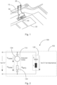
- Fig. 1 shows a sketch of a power module 10 with electronic components including power components such as semiconductor dies 30.
- a temperature sensor 40 such as a Negative Temperature Coefficient Thermistor (NTC) is arranged inside the power module 10.
- the NTC 40 is bonded to a substrate inside the power module 10 and bond wires 50 are lead to the terminals 20. Consequently, a magnetic coupling arises between the power loop defined by the devices and connections, through which high currents are running and the loop that is spanned by the bond wires 50 between the NTC 40 and the terminals 20. Due to this magnetic coupling, a switching-frequent voltage proportional to the dl/dt in the power path is induced along the bond wires 50 of the NTC 40.
- the amplitude of this voltage can be significant, for example about 500mV.
- This voltage is superimposed on the measurement. Due to a dissipation limit inside the NTC of typically 20mW, the voltage across the NTC is limited to about 1V, so that the induced voltage is in the same range as the voltage used to measure the NTC's resistance distorting the measurement. Therefore, the environment in which the temperature measurement arrangement is located is a noise voltage-inducing environment, caused by the magnetic coupling.
- a temperature measurement arrangement 100 that compensates the induced noise voltage in such an environment is shown in Fig. 2 .
- the temperature-sensing device is a resistor R_NTC 102, which is subject to the induced noise voltage, resulting in the NTC arrangement 110 including the noise voltage source 104.
- the noise voltage is switching-frequent. That is, the power devices 30, for example, semiconductors such as IGBTs, MOSFETs, etc., are switched at a certain frequency, for example 20 KHz, which causes the induced voltage.
- This induced noise voltage has as spectrum with a main peak at the same frequency, i.e., 20 kHz in this example.
- the noise voltage can be considered as noise voltage source 104 in series with the NTC, since it superimposes the actual voltage caused by the measurement current and the temperature dependent resistance of the NTC 102.
- the filter 120 is arranged in parallel to the terminals 20 of the NTC.
- the type of filter suitable for this task is therefore a notch filter 120 as shown in Fig. 2 .
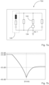
- An example of the frequency response of a notch filter with a resonance frequency at 20 KHz is shown in Fig. 3 .
- the notch filter 120 represents a very low impedance, which would be ideally 0 Ohms, but which is practically limited to the parasitic series resistance of the capacitor C and inductor L.
- the filter 120 short-circuits or nearly short-circuits the voltage of the series arrangement of NTC 102 and induced voltage represented by the noise voltage source 104 at the noise frequency, which is typically the switching frequency.
- the induced voltage is thus compensated at this frequency.
- the filter has further resonance frequencies.
- the noise voltage V_noise is negatively applied to the NTC resistance and the voltage that is measured at the module terminals, which is the sum of the noise source 104 and the voltage across the NTC resistance 102, is therefore close to zero. Independently of the circuit that is used to actually measure the NTC resistance 102.
- a low-pass filter would also be possible, which lets pass only frequencies below the switching frequency.
- a second notch filter in parallel to the notch filter may be applied. In this way, also other components of the spectrum of the induced noise voltage can be taken into account.
- the notch filter in Fig. 2 consists of a capacitor and an inductor. Depending on the requirements, e.g. width and slope of the frequency response of the filter, a more complex arrangement may be implemented.
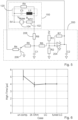
- Fig. 4 shows a schematic of the resistance-to-frequency converter 200, which is in an embodiment used as one measurement instance or evaluation instance of the entire temperature measurement arrangement.
- the resistance-to-frequency converter 200 uses a comparator 204 and a bipolar transistor 206, in this case a pnp transistor, as active elements.
- the bias resistor R1, 208 is used to narrow down the frequency range.
- the charging time of timing capacitor C1 is responsible for the measurement frequency. Its capacity and the temperature dependent resistance of the NTC 102 determine the charging time up to a voltage value equal to the reference voltage value of the comparator 204.
- the noise source is again represented as serial voltage source 104.
- the further elements in the schematics represent circuits for realizing the voltage comparison by comparator 204 and the discharging of the timing capacitor C1.
- the circuit for realizing the comparator 204 consists of the voltage divider R1, R2 for providing the reference voltage at the inverting input of the comparator 204, the current limiting resistor R6 for limiting the input current into the comparator 204, and a feedback resistor R7.
- the circuit for realizing the discharging the timing capacitor C1 consists of the bipolar pnp transistor 206 with current limiting resistors R5 at the emitter of the pnp transistor 206 and R4 at the base of the transistor 206.
- the transistor 206 is switched for discharging by applying the output voltage of comparator 204 to the base of transistor 206 via resistor R4.
- Resistor 208 also designated as R1 in Fig. 4 , is used for narrowing down frequency range of the measurement frequency, i.e., the output frequency of the resistance-to-frequency converter 200.
- Fig. 5 shows a schematic in which the resistance-to-frequency converter 200 is applied to the sensing circuit 150 that includes the NTC 102, the serial voltage source 104, and the notch filter 120.
- the timing capacitor C1 is charged by the current through NTC 102 and R8, which depends on the supply voltage, e.g., 5V plus V_noise 104 and the value of R8.
- the output frequency corresponding to the temperature sensed by the NTC 120 is provided at capacitor C2 that represents e.g. an oscilloscope probe and/or the input capacitance of a microcontroller's pin for detecting the measurement frequency.
- Fig. 6 shows a diagram with the charging time of the timing capacitor C1 for the different cases together with their error markers.
- the LC notch filter is clearly leading to very small errors compared to the uncompensated or the resistively compensated cases.
- Fig. 7a shows a schematic of sensing circuit 700 corresponding to the sensing circuit 150 with a notch filter 120 realized by an LC series connection.
- Fig. 7b shows a diagram of the frequency response of the sensing circuit 700 corresponding to the sensing circuit 150 with the notch filter 120 as shown in Fig. 7a according to a simulation.
- the damping at the switching frequency 20 kHz is higher than 65 dB.
- the results of the sensing circuit 150 with the notch filter 120 are compared to a sensing circuit 800 without compensation as shown in the schematics depicted in Fig. 8a and a sensing circuit 900 with a resistor 902 as compensating element as shown in the schematics depicted in Fig. 9a.
- Figs. 8b and 9b show the respective frequency responses.
- the damping at 20 kHz is 2.3 dB
- the damping at 20 kHz is 5.2 dB.
- Figs. 10a, 10b, and 10c show the influence of the power path current on the charging time of the capacitor, which is used as a measure for the NTC resistance.
- the switching signal I_AC 1002 of the power devices 30 in the power module 10 is represented by the dotted curves.
- the amplitude is +/- 150 A.
- Fig. 10a shows the charging time 1011 of the timing capacitor C1 without compensation.
- Fig. 10b shows the charging time 1012 of the timing capacitor with a resistor 902 as filter
- Fig. 10c shows the charging time 1012 of the timing capacitor C1 with a notch filter 120.
- notch filter compensation shown in Fig. 10c reduces the measurement noise significantly compared to a 2 kOhm compensation as shown in Fig. 10b , which again shows a reduced measurement noise compared to no compensation as shown in Fig. 10 a.
Landscapes
- Physics & Mathematics (AREA)
- General Physics & Mathematics (AREA)
- Nonlinear Science (AREA)
- Engineering & Computer Science (AREA)
- Microelectronics & Electronic Packaging (AREA)
- Electromagnetism (AREA)
- Measurement Of Current Or Voltage (AREA)
- Measuring Temperature Or Quantity Of Heat (AREA)
Abstract
Description
- The invention relates to a temperature measurement arrangement for measuring a temperature in a noise voltage-inducing environment such as a power module with switched semiconductors, a power module and a usage of a notch filter.
- For monitoring reasons and, for example, also for loss measurements, the temperature of semiconductor dies inside a power module is of high interest. For this reason, usually, an NTC is directly integrated on the substrate, preferably close to the semiconductor dies in order to estimate their temperature as accurately as possible. The close thermal coupling of the NTC to the semiconductor dies comes with a price, namely a significant magnetic coupling between the power loop and the loop that is spanned by the bond wires between the NTC and its terminals. Due to this magnetic coupling, a switching-frequent voltage proportional to the dl/dt in the power path is induced along the bond wires of the NTC. This voltage can be of a significant amplitude and is superimposed on the measurement. The induced voltage is in the same range as the voltage used to measure the NTC's resistance. Therefore, and independently of the measurement method, the measurement is typically strongly distorted and of poor accuracy during operation of the power device.
- There may be a desire to provide an arrangement that improves the temperature measurement.
- The problem is solved by the subject-matter of the independent claims. Embodiments are provided by the dependent claims, the following description and the accompanying figures.
- The described embodiments similarly pertain to the temperature measurement arrangement for measuring a temperature in a noise voltage inducing environment, a power module and a usage of a notch filter. Synergetic effects may arise from different combinations of the embodiments although they might not be described in detail.
- Technical terms are used by their common sense. If a specific meaning is conveyed to certain terms, definitions of terms will be given in the following in the context of which the terms are used.
- According to an aspect, a temperature measurement arrangement for measuring a temperature in a noise voltage-inducing environment is provided. The temperature measurement arrangement comprises a sensing circuit including a Negative Temperature Coefficient Thermistor (NTC) for sensing a temperature; and a filter for compensating the induced noise voltage at a filter frequency.
- The temperature measurement arrangement is an electrical circuit that comprises means to sense a temperature in the noise voltage-inducing environment. Herein, these means include a NTC that senses the temperature by changing its resistance in dependence on the temperature. In a noise voltage-inducing environment, the NTC is subject to a voltage superimposed to the voltage at the NTC, for example, the supply voltage for the NTC. More specifically, the bond wires from the solder points of the NTC to the terminals of the NTC form a loop through which flows a magnetic field that changes with time and induces the noise voltage. The magnetic field is caused by switched power devices nearby the loop formed by the bond wires. The noise voltage therefore has at least a frequency component at the switching frequency. The filter may be a resistor or a frequency dependent filter that filters at least a frequency, which has the same value as the switching frequency and is implemented such that it compensates the noise voltage at this frequency. "Compensating" means neutralizing the effect of the noise voltage at least in parts, i.e. not necessarily completely. Further, the effect of the noise voltage is that the voltage at the NTC varies, leading to a higher current through the NTC and thus to a noisy measurement if the further measurement circuit uses this current for measurements and evaluation. The noise voltage is represented in this disclosure as a voltage source in the schematics.
- According to an embodiment, the filter of the temperature measurement arrangement is arranged in parallel to the NTC.
- The filter may be arranged in parallel to the NTC. More specifically, the filter is arranged such that it is parallel to the noise voltage source and the NTC, which are not separable and which are represented as a series connection in an equivalent circuit diagram.
- According to an embodiment, the filter is a notch filter.
- The notch filter filters one distinct frequency, which in this case is the switching frequency of the power devices. In other words, the notch filter has a low impedance, ideally zero, at the switching frequency thereby short-circuiting, or nearly short-circuiting the series connection of the NTC and the noise voltage source.
- According to an embodiment, the temperature measurement arrangement further comprises a resistance-to-frequency converter, and wherein the sensing circuit is connected to the resistance-to-frequency converter for measuring a frequency corresponding to a resistance value of the NTC.
- That is, a known relation between a value of the NTC and the frequency is used to measure the temperature. The filtering is effective when using a resistance-to-frequency converter. As explained below in more detail, the resistance-to-frequency converter is realized for example by charging a timing capacity. The timing capacity is charged by the current dependent on the current value of the NTC. If the voltage at the timing capacity is "high", a comparator changes its output voltage and discharges the capacity again using, for example, a further active semiconductor. If the supply voltage of the NTC is not constant, which is the case here due to the superimposed noise voltage, the current for charging the timing capacitor is influenced leading to a noisy or even wrong or biased measurement.
- According to an embodiment, the temperature measurement arrangement further comprises a voltage divider or a Wheatstone bridge for measuring the resistance value of the NTC.
- A voltage divider or a Wheatstone bridge are alternative circuits that may be used for measuring the resistance value of the NTC. The filter is connected in parallel to the resistor to be measured, that is, the NTC including the unwanted voltage noise source.
- These alternative measurement circuits are simpler to realize, however their output signal is still analog and needs to be digitalized while the resistance-to-frequency converter directly generates a digital output signal that is more robust for transmission and easy to read in by a microprocessor or programmagle logic device. Nevertheless, the filter can be applied effectively also in these cases, improving the measurement results.
- According to an embodiment, the temperature measurement arrangement is integrated into a power electronic converter system.
- A power electronic converter system is one application where power components are used and the temperature is measured such that the high currents produce the noise voltage and thus the noise voltage-inducing environment.
- According to an embodiment, the NTC is arranged inside a power module.
- A power module is a device with a housing containing the power semiconductors and the NTC. As explained above, the switched current, which is running through the power module, i.e., through the power semiconductors generates the noise voltage-inducing environment inside the power module. The term "module" relates to a modular device.
- According to an embodiment, the NTC is arranged in vicinity of a switched power semiconductor, and the NTC is connected to the resistance-to-frequency converter through bond wires.
- The closer the NTC is placed to a switched power semiconductor or semiconductor die, the better the measurement becomes a representation of the actual die temperature, however at the price of higher induced noise. Using the filter as described herein therefore allows placing the NTC in even closer vicinity of a switched power semiconductor thereby maintaining or nearly maintaining the accuracy as if the NTC would be placed further away from the semiconductor die.
- According to an embodiment, a switching frequency of the switched semiconductor corresponds to the resonance frequency of the filter.
- "Corresponds" means that the two frequencies are the same, or nearly the same. In embodiments, "correspond" may mean further that the filter has for example additional resonance frequencies, which are harmonics of the switching frequency.
- According to an embodiment, a frequency of the resistance-to-frequency converter corresponding to the resistance of the NTC differs from the switching frequency of the semiconductor by at least one decade.
- A pre-requirement for the proper functionality of the measurement is that the measurement frequency and the frequency of the noise source, which is usually the switching frequency, must be significantly separated by, for example, at least one decade, i.e., at least 10 times higher than the switching frequency. In case of a voltage divider of a Wheatstone bridge, the pre-requirement of significantly separated frequencies is fulfilled automatically and the notch filter does not have any impact on the DC measurement.
- If the frequencies were equal or similar, the measurement signal could hardly be distinguished from the induced noise and therefore the measurement could be biased. If the frequencies differ significantly, a remaining ripple in the measurement output can be averaged out.
- According to an embodiment, resistance-to-frequency converter is connected to the sensing circuit through a connecting resistor configured to provide a current to the resistance-to-frequency converter for generating an oscillating voltage in dependence on the value of the current from the connecting resistor.
- The oscillating voltage is also referred to as measurement voltage or measurement output voltage of the resistance-to-frequency converter. The timing capacitor is charged with the current from the NTC through the connecting resistor.
- According to an embodiment, the resistance-to-frequency converter comprises a comparator, a bipolar transistor, and a timing capacitor. The timing capacitor is connected to the NTC and to the comparator for switching the comparator to generate the oscillating voltage, and the comparator is connected to the bipolar transistor for controlling the discharging of the timing capacitor.
- That is, the resistance-to-frequency converter comprises a comparator and a bipolar transistor as active elements. The timing capacitor voltage triggers the switching of the comparator, which again controls the transistor for discharging the timing capacitor such that an oscillation is generated. The charging time of the timing capacitor is determined by the temperature dependent resistance of the NTC
- More specifically, the NTC is arranged between the supply voltage of the measurement circuit and the connecting resistor. The same applies to the filter. The connecting resistor is connected to a first terminal of the timing capacitor, whose second terminal is further connected to ground. The voltage of the timing capacitor is input to the comparator. That is, the first terminal of the timing capacitor is connected for example via a current limiting resistor to the inverting input pin of the comparator. The reference voltage of the comparator may be provided to the non-inverting input pin of the comparator and might be realized by a voltage divider. By the voltage divider, the frequency range of the measurement frequency can be limited. This may be realized using a bias resistor, which may be one of the resistors of the voltage divider providing the reference voltage.
- The output of the comparator is connected to the base of a pnp transistor in order to control the discharging of the timing capacitor whose first terminal is connected to the emitter of the pnp transistor and whose collector is connected to ground. Of course, circuits fulfilling the same function may replace devices described herein, and the converter may comprise additional devices. Thus, the functionalities such as the connection between the sensing circuit and the converter, the discharging of the timing capacitor or the comparison may be realized in alternative ways that are known to a skilled person.
- According to an embodiment, power module comprising a temperature measurement arrangement as described herein is provided.
- According to an embodiment, the power module comprises at least one of an Insulated-Gate Bipolar Transistor (IGBT), a diode, a Silicon Carbid (SiC) MOSFET, an Integrated Gate Commutated Thyristors (IGCT), and a Galliumnitrid High-Electron-Mobility Transistor (GaN HEMT).
- According to an embodiment, a usage of a notch filter in a temperature measurement arrangement as described herein is provided.
-
- Fig. 1
- shows a sketch of a power module,
- Fig. 2
- shows a schematic of the sensing circuit including an NTC resistor,
- Fig. 3
- shows a diagram of the frequency response of a notch filter,
- Fig. 4
- shows a schematic of the resistance-to-frequency converter,
- Fig. 5
- shows a schematic, in which the resistance-to-frequency converter is applied to the sensing circuit,
- Fig. 6
- shows a diagram with the charging time of the timing capacitor for the different cases,
- Fig. 7a
- shows a schematic of a sensing circuit with a notch filter,
- Fig. 7b
- shows a diagram of the frequency response of the sensing circuit depicted in
Fig. 7a - Fig. 8a
- shows a schematic of a sensing circuit without a filter,
- Fig. 8b
- shows a diagram of the frequency response of the sensing circuit depicted in
Fig. 8a , - Fig. 9a
- shows a schematic of a sensing circuit with a parallel resistor,
- Fig. 9b
- shows a diagram of the frequency response of the sensing circuit depicted in
Fig. 9a , - Fig. 10a
- shows the charging time of the timing capacitor without compensation,
- Fig. 10b
- shows the charging time of the timing capacitor with a resistor as filter,
- Fig. 10c
- shows the charging time of the timing capacitor with a notch filter.
- Corresponding parts are provided with the same reference symbols in all figures.
-
Fig. 1 shows a sketch of apower module 10 with electronic components including power components such as semiconductor dies 30. Atemperature sensor 40, such as a Negative Temperature Coefficient Thermistor (NTC) is arranged inside thepower module 10. TheNTC 40 is bonded to a substrate inside thepower module 10 andbond wires 50 are lead to theterminals 20. Consequently, a magnetic coupling arises between the power loop defined by the devices and connections, through which high currents are running and the loop that is spanned by thebond wires 50 between theNTC 40 and theterminals 20. Due to this magnetic coupling, a switching-frequent voltage proportional to the dl/dt in the power path is induced along thebond wires 50 of theNTC 40. The amplitude of this voltage can be significant, for example about 500mV. This voltage is superimposed on the measurement. Due to a dissipation limit inside the NTC of typically 20mW, the voltage across the NTC is limited to about 1V, so that the induced voltage is in the same range as the voltage used to measure the NTC's resistance distorting the measurement. Therefore, the environment in which the temperature measurement arrangement is located is a noise voltage-inducing environment, caused by the magnetic coupling. - A
temperature measurement arrangement 100 that compensates the induced noise voltage in such an environment is shown inFig. 2 . The temperature-sensing device is aresistor R_NTC 102, which is subject to the induced noise voltage, resulting in theNTC arrangement 110 including thenoise voltage source 104. As already explained, the noise voltage is switching-frequent. That is, thepower devices 30, for example, semiconductors such as IGBTs, MOSFETs, etc., are switched at a certain frequency, for example 20 KHz, which causes the induced voltage. This induced noise voltage has as spectrum with a main peak at the same frequency, i.e., 20 kHz in this example. The noise voltage can be considered asnoise voltage source 104 in series with the NTC, since it superimposes the actual voltage caused by the measurement current and the temperature dependent resistance of theNTC 102. - For short-circuiting the induced voltage at least at the switching frequency, the
filter 120 is arranged in parallel to theterminals 20 of the NTC. The type of filter suitable for this task is therefore anotch filter 120 as shown inFig. 2 . An example of the frequency response of a notch filter with a resonance frequency at 20 KHz is shown inFig. 3 . For the noise voltage frequency, thenotch filter 120 represents a very low impedance, which would be ideally 0 Ohms, but which is practically limited to the parasitic series resistance of the capacitor C and inductor L. That is, thefilter 120 short-circuits or nearly short-circuits the voltage of the series arrangement ofNTC 102 and induced voltage represented by thenoise voltage source 104 at the noise frequency, which is typically the switching frequency. The induced voltage is thus compensated at this frequency. In embodiments, the filter has further resonance frequencies. - Due to this, the noise voltage V_noise is negatively applied to the NTC resistance and the voltage that is measured at the module terminals, which is the sum of the
noise source 104 and the voltage across theNTC resistance 102, is therefore close to zero. Independently of the circuit that is used to actually measure theNTC resistance 102. - Alternatively, a low-pass filter would also be possible, which lets pass only frequencies below the switching frequency. Further, instead of a single notch filter, a second notch filter in parallel to the notch filter may be applied. In this way, also other components of the spectrum of the induced noise voltage can be taken into account.
- The notch filter in
Fig. 2 consists of a capacitor and an inductor. Depending on the requirements, e.g. width and slope of the frequency response of the filter, a more complex arrangement may be implemented. -
Fig. 4 shows a schematic of the resistance-to-frequency converter 200, which is in an embodiment used as one measurement instance or evaluation instance of the entire temperature measurement arrangement. The resistance-to-frequency converter 200 uses acomparator 204 and abipolar transistor 206, in this case a pnp transistor, as active elements. The bias resistor R1, 208, is used to narrow down the frequency range. The charging time of timing capacitor C1 is responsible for the measurement frequency. Its capacity and the temperature dependent resistance of theNTC 102 determine the charging time up to a voltage value equal to the reference voltage value of thecomparator 204. The noise source is again represented asserial voltage source 104. The further elements in the schematics represent circuits for realizing the voltage comparison bycomparator 204 and the discharging of the timing capacitor C1. For example, the circuit for realizing thecomparator 204 consists of the voltage divider R1, R2 for providing the reference voltage at the inverting input of thecomparator 204, the current limiting resistor R6 for limiting the input current into thecomparator 204, and a feedback resistor R7. The circuit for realizing the discharging the timing capacitor C1 consists of thebipolar pnp transistor 206 with current limiting resistors R5 at the emitter of thepnp transistor 206 and R4 at the base of thetransistor 206. Thetransistor 206 is switched for discharging by applying the output voltage ofcomparator 204 to the base oftransistor 206 via resistor R4.Resistor 208, also designated as R1 inFig. 4 , is used for narrowing down frequency range of the measurement frequency, i.e., the output frequency of the resistance-to-frequency converter 200. -
Fig. 5 shows a schematic in which the resistance-to-frequency converter 200 is applied to thesensing circuit 150 that includes theNTC 102, theserial voltage source 104, and thenotch filter 120. The timing capacitor C1 is charged by the current throughNTC 102 and R8, which depends on the supply voltage, e.g.,5V plus V_noise 104 and the value of R8. The output frequency corresponding to the temperature sensed by theNTC 120 is provided at capacitor C2 that represents e.g. an oscilloscope probe and/or the input capacitance of a microcontroller's pin for detecting the measurement frequency. -
Fig. 6 shows a diagram with the charging time of the timing capacitor C1 for the different cases together with their error markers. The LC notch filter is clearly leading to very small errors compared to the uncompensated or the resistively compensated cases. -
Fig. 7a shows a schematic ofsensing circuit 700 corresponding to thesensing circuit 150 with anotch filter 120 realized by an LC series connection. -
Fig. 7b shows a diagram of the frequency response of thesensing circuit 700 corresponding to thesensing circuit 150 with thenotch filter 120 as shown inFig. 7a according to a simulation. The damping at theswitching frequency 20 kHz is higher than 65 dB. - The results of the
sensing circuit 150 with thenotch filter 120 are compared to asensing circuit 800 without compensation as shown in the schematics depicted inFig. 8a and asensing circuit 900 with aresistor 902 as compensating element as shown in the schematics depicted inFig. 9a. Figs. 8b and 9b show the respective frequency responses. In case of no compensation, the damping at 20 kHz is 2.3 dB, and in case of having aresistor 902 as compensating element, the damping at 20 kHz is 5.2 dB. -
Figs. 10a, 10b, and 10c show the influence of the power path current on the charging time of the capacitor, which is used as a measure for the NTC resistance. In the Figures, theswitching signal I_AC 1002 of thepower devices 30 in thepower module 10 is represented by the dotted curves. The amplitude is +/- 150 A.Fig. 10a shows the charging time 1011 of the timing capacitor C1 without compensation.Fig. 10b shows thecharging time 1012 of the timing capacitor with aresistor 902 as filter, andFig. 10c shows thecharging time 1012 of the timing capacitor C1 with anotch filter 120. - It is evident that the notch filter compensation shown in
Fig. 10c reduces the measurement noise significantly compared to a 2 kOhm compensation as shown inFig. 10b , which again shows a reduced measurement noise compared to no compensation as shown inFig. 10 a. - Other variations to the disclosed embodiments can be understood and effected by those skilled in the art in practicing the claimed invention, from the study of the drawings, the disclosure, and the appended claims. In the claims, the word "comprising" does not exclude other elements or steps and the indefinite article "a" or "an" does not exclude a plurality. A single processor or other unit may fulfill the functions of several items or steps recited in the claims. The mere fact that certain measures are recited in mutually different dependent claims does not indicate that a combination of these measures cannot be used to advantage. Any reference signs in the claims should not be construed as limiting the scope of the claims.
-
- 10
- Power module
- 20
- Terminals of a Temperature sensor/NTC
- 30
- Electronic components / power devices inside the power module
- 40
- Temperature sensor/NTC inside the power module
- 50
- Bond wires
- 100
- Temperature measurement arrangement
- 102
- NTC, R_NTC
- 104
- Noise voltage source, V_noise
- 110
- NTC arrangement: R_NTC including noise voltage source
- 120
- Filter
- 150
- Sensing circuit
- 200
- Resistance-to-frequency converter
- 204
- Comparator
- 206
- Transistor, bipolar pnp transistor
- 208
- Resistor for narrowing down frequency range
- 700
- Sensing circuit with LC filter / notch filter
- 800
- Sensing circuit without compensation
- 900
- Sensing circuit with a resistor
- 902
- Resistor of
sensing circuit 900 - 1002
- Switching signal IAC of the power devices in the power module
- 1011
- Charging time of the timing capacitor without compensation
- 1012
- Charging time of the timing capacitor with a resistor as filter
- 1013
- Charging time of the timing capacitor with a notch filter
Claims (15)
- Temperature measurement arrangement (100) for measuring a temperature in a noise voltage-inducing environment comprising a sensing circuit (150) includinga Negative Temperature Coefficient Thermistor, NTC, (102) for sensing a temperature; anda filter (120) for compensating the induced noise voltage at a filter frequency.
- Temperature measurement arrangement (100) according to claim 1, wherein the filter (120) is arranged in parallel to the NTC (102).
- Temperature measurement arrangement (100) according to claim 1 or 2, wherein the filter (120) is a notch filter (120).
- Temperature measurement arrangement (100) according to any one of the previous claims, wherein the temperature measurement arrangement (100) further comprises a resistance-to-frequency converter (200), and wherein the sensing circuit (150) is connected to the resistance-to-frequency converter (200) for measuring a frequency corresponding to a resistance value of the NTC (102).
- Temperature measurement arrangement (100) according to any one of the claims 1-3, wherein the temperature measurement arrangement (100) further comprises a voltage divider or a Wheatstone bridge for measuring the resistance value of the NTC (102).
- Temperature measurement arrangement (100) according to any one of the previous claims, wherein the temperature measurement arrangement (100) is integrated into a power electronic converter system.
- Temperature measurement arrangement (100) according to any one of the previous claims, wherein the NTC (102) is arranged inside a power module (10).
- Temperature measurement arrangement (100) according to any one of the previous claims, wherein the NTC (102) is arranged in vicinity of a switched power semiconductor, and the NTC (102) is connected to the resistance-to-frequency converter (200) through bond wires (50).
- Temperature measurement arrangement (100) according to any one of the previous claims, wherein a switching frequency of the switched semiconductor corresponds to the resonance frequency of the filter (120).
- Temperature measurement arrangement (100) according to any one of the claims 4 and 6-9, wherein a frequency of the resistance-to-frequency converter (200) corresponding to the resistance of the NTC (102) differs from the switching frequency of the semiconductor by at least one decade.
- Temperature measurement arrangement (100) according to any one of the claims 4 and 6-10, wherein the resistance-to-frequency converter (200) is connected to the sensing circuit (150) through a connecting resistor configured to provide a current to the resistance-to-frequency converter (200) for generating an oscillating voltage in dependence on the value of the current from the connecting resistor.
- Temperature measurement arrangement (100) according to any one of the claims 4 and 6-10, wherein the resistance-to-frequency converter (200) comprises a comparator (204), a bipolar transistor (206), and a timing capacitor;wherein the timing capacitor is connected to the NTC (102) and to the comparator (204) for switching the comparator (204) to generate the oscillating voltage; andwherein the comparator (204) is connected to the bipolar transistor (206) for controlling the discharging of the timing capacitor.
- Power module (10) comprising a temperature measurement arrangement (100) according to claim 1.
- Power module (10) according to claim 13, wherein the power module (10) comprises at least one of an IGBT, a diode, a SiC MOSFET, an IGCT, and a GaN HEMT.
- Usage of a notch filter (120) in a temperature measurement arrangement (100) according to claim 1.
Priority Applications (3)
| Application Number | Priority Date | Filing Date | Title |
|---|---|---|---|
| EP22185530.7A EP4310472A1 (en) | 2022-07-18 | 2022-07-18 | Temperature measurement arrangement in a power module |
| CN202310875164.8A CN117419822A (en) | 2022-07-18 | 2023-07-17 | Temperature measuring device in power module |
| US18/354,042 US20240019315A1 (en) | 2022-07-18 | 2023-07-18 | Temperature Measurement Arrangement in a Power Module |
Applications Claiming Priority (1)
| Application Number | Priority Date | Filing Date | Title |
|---|---|---|---|
| EP22185530.7A EP4310472A1 (en) | 2022-07-18 | 2022-07-18 | Temperature measurement arrangement in a power module |
Publications (1)
| Publication Number | Publication Date |
|---|---|
| EP4310472A1 true EP4310472A1 (en) | 2024-01-24 |
Family
ID=82655178
Family Applications (1)
| Application Number | Title | Priority Date | Filing Date |
|---|---|---|---|
| EP22185530.7A Pending EP4310472A1 (en) | 2022-07-18 | 2022-07-18 | Temperature measurement arrangement in a power module |
Country Status (3)
| Country | Link |
|---|---|
| US (1) | US20240019315A1 (en) |
| EP (1) | EP4310472A1 (en) |
| CN (1) | CN117419822A (en) |
Families Citing this family (2)
| Publication number | Priority date | Publication date | Assignee | Title |
|---|---|---|---|---|
| JP2025151347A (en) * | 2024-03-28 | 2025-10-09 | 新電元工業株式会社 | Semiconductor Module |
| CN121096906A (en) * | 2025-04-01 | 2025-12-09 | 深圳市鹏芯微集成电路制造有限公司 | Semiconductor temperature measuring device |
Citations (5)
| Publication number | Priority date | Publication date | Assignee | Title |
|---|---|---|---|---|
| CN208902298U (en) * | 2018-08-16 | 2019-05-24 | 江苏镇安欣润电力科技有限公司 | A kind of IGBT temperature detection circuit |
| CN110044510A (en) * | 2019-05-17 | 2019-07-23 | 上海希形科技有限公司 | IGBT module temperature measurement circuit, temp measuring method and computer readable storage medium |
| WO2021182012A1 (en) * | 2020-03-10 | 2021-09-16 | 株式会社デンソー | Temperature detection device |
| WO2021199418A1 (en) * | 2020-04-03 | 2021-10-07 | 三菱電機株式会社 | Temperature detecting circuit |
| CN215865544U (en) * | 2021-04-02 | 2022-02-18 | 广东朝阳电子科技股份有限公司 | Power supply structure of temperature sampling circuit of Bluetooth headset |
Family Cites Families (5)
| Publication number | Priority date | Publication date | Assignee | Title |
|---|---|---|---|---|
| US6129673A (en) * | 1998-06-08 | 2000-10-10 | Advanced Monitors, Corp. | Infrared thermometer |
| US6902318B2 (en) * | 2001-02-15 | 2005-06-07 | Oppama Industry Co., Ltd. | Thermometer for engine of vehicle |
| US7877022B2 (en) * | 2006-07-07 | 2011-01-25 | Walid Kamali | Circuits and methods of thermal gain compensation |
| US12156546B2 (en) * | 2019-04-23 | 2024-12-03 | Philip Morris Products S.A. | Aerosol-generating device with puff detection and method for puff detection |
| US20220018720A1 (en) * | 2020-07-20 | 2022-01-20 | Dana Tm4 Inc. | Sensing junction temperature of power transistors |
-
2022
- 2022-07-18 EP EP22185530.7A patent/EP4310472A1/en active Pending
-
2023
- 2023-07-17 CN CN202310875164.8A patent/CN117419822A/en active Pending
- 2023-07-18 US US18/354,042 patent/US20240019315A1/en active Pending
Patent Citations (5)
| Publication number | Priority date | Publication date | Assignee | Title |
|---|---|---|---|---|
| CN208902298U (en) * | 2018-08-16 | 2019-05-24 | 江苏镇安欣润电力科技有限公司 | A kind of IGBT temperature detection circuit |
| CN110044510A (en) * | 2019-05-17 | 2019-07-23 | 上海希形科技有限公司 | IGBT module temperature measurement circuit, temp measuring method and computer readable storage medium |
| WO2021182012A1 (en) * | 2020-03-10 | 2021-09-16 | 株式会社デンソー | Temperature detection device |
| WO2021199418A1 (en) * | 2020-04-03 | 2021-10-07 | 三菱電機株式会社 | Temperature detecting circuit |
| CN215865544U (en) * | 2021-04-02 | 2022-02-18 | 广东朝阳电子科技股份有限公司 | Power supply structure of temperature sampling circuit of Bluetooth headset |
Non-Patent Citations (1)
| Title |
|---|
| NATARAJAN S: "Widely Linear Temperature-to-Frequency Converters", IEEE TRANSACTIONS ON INSTRUMENTATION AND MEASUREMENT,, vol. IM-24, no. 3, 1 September 1975 (1975-09-01), pages 235 - 239, XP001412250 * |
Also Published As
| Publication number | Publication date |
|---|---|
| US20240019315A1 (en) | 2024-01-18 |
| CN117419822A (en) | 2024-01-19 |
Similar Documents
| Publication | Publication Date | Title |
|---|---|---|
| US20240019315A1 (en) | Temperature Measurement Arrangement in a Power Module | |
| US6400163B1 (en) | Circuit arrangement for monitoring an electronic switch controlling a load | |
| CN105556266B (en) | Method and apparatus for determining the actual junction temperature of an IGBT device | |
| JP4360202B2 (en) | Phase current detector | |
| Wang et al. | Infinity sensor: Temperature sensing in GaN power devices using peak di/dt | |
| Funk et al. | An integrated and galvanically isolated DC-to-15.3 MHz hybrid current sensor | |
| CN113949327B (en) | Power modules for operating electric vehicle drives | |
| CN104024814B (en) | Devices for measuring the temperature of power semiconductors | |
| Denk et al. | IGBT gate driver with accurate measurement of junction temperature and inverter output current | |
| Koch et al. | Design methodology for ultra-compact rogowski coils for current sensing in low-voltage high-current gan based dc/dc-converters | |
| US5226319A (en) | Hot wire air flow meter | |
| JPH06281693A (en) | Method for measuring thermal resistance of semiconductor device | |
| CN100563090C (en) | Phase current detector | |
| CN112752959B (en) | Temperature measurement of power semiconductor switching elements | |
| JP2003075487A (en) | Impedance detection device and capacitance detection device | |
| CN107535019A (en) | For the method for the power control circuit for calibrating induced cooking utensils | |
| JPH0261695B2 (en) | ||
| Fröhling et al. | Contact-integrated temperature measurement for power modules | |
| JPH08271204A (en) | Eddy current type displacement sensor | |
| US12607585B2 (en) | Method for measuring degradation of thermal resistance between power semiconductor and heat sink, and control device for power semiconductor | |
| JP2003207529A (en) | Sensor capacitance detecting device and sensor capacitance detecting method | |
| US7443232B2 (en) | Active load arrangement | |
| JP3019624B2 (en) | Current detector | |
| JPH05149996A (en) | Method for measuring thermal resistance of semiconductor device | |
| JPH08247815A (en) | Pulse output type hot wire air flow meter |
Legal Events
| Date | Code | Title | Description |
|---|---|---|---|
| PUAI | Public reference made under article 153(3) epc to a published international application that has entered the european phase |
Free format text: ORIGINAL CODE: 0009012 |
|
| STAA | Information on the status of an ep patent application or granted ep patent |
Free format text: STATUS: THE APPLICATION HAS BEEN PUBLISHED |
|
| AK | Designated contracting states |
Kind code of ref document: A1 Designated state(s): AL AT BE BG CH CY CZ DE DK EE ES FI FR GB GR HR HU IE IS IT LI LT LU LV MC MK MT NL NO PL PT RO RS SE SI SK SM TR |
|
| STAA | Information on the status of an ep patent application or granted ep patent |
Free format text: STATUS: REQUEST FOR EXAMINATION WAS MADE |
|
| 17P | Request for examination filed |
Effective date: 20240723 |
|
| RBV | Designated contracting states (corrected) |
Designated state(s): AL AT BE BG CH CY CZ DE DK EE ES FI FR GB GR HR HU IE IS IT LI LT LU LV MC MK MT NL NO PL PT RO RS SE SI SK SM TR |
|
| STAA | Information on the status of an ep patent application or granted ep patent |
Free format text: STATUS: EXAMINATION IS IN PROGRESS |
|
| 17Q | First examination report despatched |
Effective date: 20251111 |