EP4307565A1 - Substrate, production method for substrate, and production method for unit cell - Google Patents
Substrate, production method for substrate, and production method for unit cell Download PDFInfo
- Publication number
- EP4307565A1 EP4307565A1 EP22766661.7A EP22766661A EP4307565A1 EP 4307565 A1 EP4307565 A1 EP 4307565A1 EP 22766661 A EP22766661 A EP 22766661A EP 4307565 A1 EP4307565 A1 EP 4307565A1
- Authority
- EP
- European Patent Office
- Prior art keywords
- alkali metal
- substrate
- metal azide
- spot
- azide
- Prior art date
- Legal status (The legal status is an assumption and is not a legal conclusion. Google has not performed a legal analysis and makes no representation as to the accuracy of the status listed.)
- Pending
Links
Images

Classifications
-
- C—CHEMISTRY; METALLURGY
- C03—GLASS; MINERAL OR SLAG WOOL
- C03C—CHEMICAL COMPOSITION OF GLASSES, GLAZES OR VITREOUS ENAMELS; SURFACE TREATMENT OF GLASS; SURFACE TREATMENT OF FIBRES OR FILAMENTS MADE FROM GLASS, MINERALS OR SLAGS; JOINING GLASS TO GLASS OR OTHER MATERIALS
- C03C17/00—Surface treatment of glass, not in the form of fibres or filaments, by coating
- C03C17/22—Surface treatment of glass, not in the form of fibres or filaments, by coating with other inorganic material
-
- G—PHYSICS
- G04—HOROLOGY
- G04F—TIME-INTERVAL MEASURING
- G04F5/00—Apparatus for producing preselected time intervals for use as timing standards
- G04F5/14—Apparatus for producing preselected time intervals for use as timing standards using atomic clocks
-
- B—PERFORMING OPERATIONS; TRANSPORTING
- B32—LAYERED PRODUCTS
- B32B—LAYERED PRODUCTS, i.e. PRODUCTS BUILT-UP OF STRATA OF FLAT OR NON-FLAT, e.g. CELLULAR OR HONEYCOMB, FORM
- B32B17/00—Layered products essentially comprising sheet glass, or glass, slag, or like fibres
- B32B17/06—Layered products essentially comprising sheet glass, or glass, slag, or like fibres comprising glass as the main or only constituent of a layer, next to another layer of a specific material
- B32B17/10—Layered products essentially comprising sheet glass, or glass, slag, or like fibres comprising glass as the main or only constituent of a layer, next to another layer of a specific material of synthetic resin
-
- B—PERFORMING OPERATIONS; TRANSPORTING
- B32—LAYERED PRODUCTS
- B32B—LAYERED PRODUCTS, i.e. PRODUCTS BUILT-UP OF STRATA OF FLAT OR NON-FLAT, e.g. CELLULAR OR HONEYCOMB, FORM
- B32B27/00—Layered products comprising a layer of synthetic resin
- B32B27/28—Layered products comprising a layer of synthetic resin comprising synthetic resins not wholly covered by any one of the sub-groups B32B27/30 - B32B27/42
- B32B27/283—Layered products comprising a layer of synthetic resin comprising synthetic resins not wholly covered by any one of the sub-groups B32B27/30 - B32B27/42 comprising polysiloxanes
-
- B—PERFORMING OPERATIONS; TRANSPORTING
- B32—LAYERED PRODUCTS
- B32B—LAYERED PRODUCTS, i.e. PRODUCTS BUILT-UP OF STRATA OF FLAT OR NON-FLAT, e.g. CELLULAR OR HONEYCOMB, FORM
- B32B3/00—Layered products comprising a layer with external or internal discontinuities or unevennesses, or a layer of non-planar shape; Layered products comprising a layer having particular features of form
- B32B3/26—Layered products comprising a layer with external or internal discontinuities or unevennesses, or a layer of non-planar shape; Layered products comprising a layer having particular features of form characterised by a particular shape of the outline of the cross-section of a continuous layer; characterised by a layer with cavities or internal voids ; characterised by an apertured layer
- B32B3/266—Layered products comprising a layer with external or internal discontinuities or unevennesses, or a layer of non-planar shape; Layered products comprising a layer having particular features of form characterised by a particular shape of the outline of the cross-section of a continuous layer; characterised by a layer with cavities or internal voids ; characterised by an apertured layer characterised by an apertured layer, the apertures going through the whole thickness of the layer, e.g. expanded metal, perforated layer, slit layer regular cells B32B3/12
-
- B—PERFORMING OPERATIONS; TRANSPORTING
- B32—LAYERED PRODUCTS
- B32B—LAYERED PRODUCTS, i.e. PRODUCTS BUILT-UP OF STRATA OF FLAT OR NON-FLAT, e.g. CELLULAR OR HONEYCOMB, FORM
- B32B3/00—Layered products comprising a layer with external or internal discontinuities or unevennesses, or a layer of non-planar shape; Layered products comprising a layer having particular features of form
- B32B3/26—Layered products comprising a layer with external or internal discontinuities or unevennesses, or a layer of non-planar shape; Layered products comprising a layer having particular features of form characterised by a particular shape of the outline of the cross-section of a continuous layer; characterised by a layer with cavities or internal voids ; characterised by an apertured layer
- B32B3/30—Layered products comprising a layer with external or internal discontinuities or unevennesses, or a layer of non-planar shape; Layered products comprising a layer having particular features of form characterised by a particular shape of the outline of the cross-section of a continuous layer; characterised by a layer with cavities or internal voids ; characterised by an apertured layer characterised by a layer formed with recesses or projections, e.g. hollows, grooves, protuberances, ribs
-
- B—PERFORMING OPERATIONS; TRANSPORTING
- B32—LAYERED PRODUCTS
- B32B—LAYERED PRODUCTS, i.e. PRODUCTS BUILT-UP OF STRATA OF FLAT OR NON-FLAT, e.g. CELLULAR OR HONEYCOMB, FORM
- B32B37/00—Methods or apparatus for laminating, e.g. by curing or by ultrasonic bonding
- B32B37/14—Methods or apparatus for laminating, e.g. by curing or by ultrasonic bonding characterised by the properties of the layers
- B32B37/16—Methods or apparatus for laminating, e.g. by curing or by ultrasonic bonding characterised by the properties of the layers with all layers existing as coherent layers before laminating
- B32B37/18—Methods or apparatus for laminating, e.g. by curing or by ultrasonic bonding characterised by the properties of the layers with all layers existing as coherent layers before laminating involving the assembly of discrete sheets or panels only
- B32B37/182—Methods or apparatus for laminating, e.g. by curing or by ultrasonic bonding characterised by the properties of the layers with all layers existing as coherent layers before laminating involving the assembly of discrete sheets or panels only one or more of the layers being plastic
-
- B—PERFORMING OPERATIONS; TRANSPORTING
- B32—LAYERED PRODUCTS
- B32B—LAYERED PRODUCTS, i.e. PRODUCTS BUILT-UP OF STRATA OF FLAT OR NON-FLAT, e.g. CELLULAR OR HONEYCOMB, FORM
- B32B38/00—Ancillary operations in connection with laminating processes
- B32B38/0004—Cutting, tearing or severing, e.g. bursting; Cutter details
-
- B—PERFORMING OPERATIONS; TRANSPORTING
- B32—LAYERED PRODUCTS
- B32B—LAYERED PRODUCTS, i.e. PRODUCTS BUILT-UP OF STRATA OF FLAT OR NON-FLAT, e.g. CELLULAR OR HONEYCOMB, FORM
- B32B38/00—Ancillary operations in connection with laminating processes
- B32B38/0008—Electrical discharge treatment, e.g. corona, plasma treatment; wave energy or particle radiation
-
- G—PHYSICS
- G04—HOROLOGY
- G04F—TIME-INTERVAL MEASURING
- G04F5/00—Apparatus for producing preselected time intervals for use as timing standards
- G04F5/14—Apparatus for producing preselected time intervals for use as timing standards using atomic clocks
- G04F5/145—Apparatus for producing preselected time intervals for use as timing standards using atomic clocks using Coherent Population Trapping
-
- H—ELECTRICITY
- H03—ELECTRONIC CIRCUITRY
- H03L—AUTOMATIC CONTROL, STARTING, SYNCHRONISATION OR STABILISATION OF GENERATORS OF ELECTRONIC OSCILLATIONS OR PULSES
- H03L7/00—Automatic control of frequency or phase; Synchronisation
- H03L7/26—Automatic control of frequency or phase; Synchronisation using energy levels of molecules, atoms, or subatomic particles as a frequency reference
-
- B—PERFORMING OPERATIONS; TRANSPORTING
- B32—LAYERED PRODUCTS
- B32B—LAYERED PRODUCTS, i.e. PRODUCTS BUILT-UP OF STRATA OF FLAT OR NON-FLAT, e.g. CELLULAR OR HONEYCOMB, FORM
- B32B2250/00—Layers arrangement
- B32B2250/03—3 layers
-
- B—PERFORMING OPERATIONS; TRANSPORTING
- B32—LAYERED PRODUCTS
- B32B—LAYERED PRODUCTS, i.e. PRODUCTS BUILT-UP OF STRATA OF FLAT OR NON-FLAT, e.g. CELLULAR OR HONEYCOMB, FORM
- B32B2250/00—Layers arrangement
- B32B2250/40—Symmetrical or sandwich layers, e.g. ABA, ABCBA, ABCCBA
-
- B—PERFORMING OPERATIONS; TRANSPORTING
- B32—LAYERED PRODUCTS
- B32B—LAYERED PRODUCTS, i.e. PRODUCTS BUILT-UP OF STRATA OF FLAT OR NON-FLAT, e.g. CELLULAR OR HONEYCOMB, FORM
- B32B2255/00—Coating on the layer surface
- B32B2255/20—Inorganic coating
-
- B—PERFORMING OPERATIONS; TRANSPORTING
- B32—LAYERED PRODUCTS
- B32B—LAYERED PRODUCTS, i.e. PRODUCTS BUILT-UP OF STRATA OF FLAT OR NON-FLAT, e.g. CELLULAR OR HONEYCOMB, FORM
- B32B2310/00—Treatment by energy or chemical effects
- B32B2310/08—Treatment by energy or chemical effects by wave energy or particle radiation
- B32B2310/0806—Treatment by energy or chemical effects by wave energy or particle radiation using electromagnetic radiation
- B32B2310/0831—Treatment by energy or chemical effects by wave energy or particle radiation using electromagnetic radiation using UV radiation
-
- B—PERFORMING OPERATIONS; TRANSPORTING
- B32—LAYERED PRODUCTS
- B32B—LAYERED PRODUCTS, i.e. PRODUCTS BUILT-UP OF STRATA OF FLAT OR NON-FLAT, e.g. CELLULAR OR HONEYCOMB, FORM
- B32B2315/00—Other materials containing non-metallic inorganic compounds not provided for in groups B32B2311/00 - B32B2313/04
- B32B2315/08—Glass
-
- B—PERFORMING OPERATIONS; TRANSPORTING
- B32—LAYERED PRODUCTS
- B32B—LAYERED PRODUCTS, i.e. PRODUCTS BUILT-UP OF STRATA OF FLAT OR NON-FLAT, e.g. CELLULAR OR HONEYCOMB, FORM
- B32B2383/00—Polysiloxanes
-
- B—PERFORMING OPERATIONS; TRANSPORTING
- B32—LAYERED PRODUCTS
- B32B—LAYERED PRODUCTS, i.e. PRODUCTS BUILT-UP OF STRATA OF FLAT OR NON-FLAT, e.g. CELLULAR OR HONEYCOMB, FORM
- B32B2457/00—Electrical equipment
-
- B—PERFORMING OPERATIONS; TRANSPORTING
- B82—NANOTECHNOLOGY
- B82Y—SPECIFIC USES OR APPLICATIONS OF NANOSTRUCTURES; MEASUREMENT OR ANALYSIS OF NANOSTRUCTURES; MANUFACTURE OR TREATMENT OF NANOSTRUCTURES
- B82Y20/00—Nanooptics, e.g. quantum optics or photonic crystals
-
- C—CHEMISTRY; METALLURGY
- C03—GLASS; MINERAL OR SLAG WOOL
- C03C—CHEMICAL COMPOSITION OF GLASSES, GLAZES OR VITREOUS ENAMELS; SURFACE TREATMENT OF GLASS; SURFACE TREATMENT OF FIBRES OR FILAMENTS MADE FROM GLASS, MINERALS OR SLAGS; JOINING GLASS TO GLASS OR OTHER MATERIALS
- C03C2217/00—Coatings on glass
- C03C2217/20—Materials for coating a single layer on glass
- C03C2217/28—Other inorganic materials
-
- C—CHEMISTRY; METALLURGY
- C03—GLASS; MINERAL OR SLAG WOOL
- C03C—CHEMICAL COMPOSITION OF GLASSES, GLAZES OR VITREOUS ENAMELS; SURFACE TREATMENT OF GLASS; SURFACE TREATMENT OF FIBRES OR FILAMENTS MADE FROM GLASS, MINERALS OR SLAGS; JOINING GLASS TO GLASS OR OTHER MATERIALS
- C03C2218/00—Methods for coating glass
- C03C2218/10—Deposition methods
- C03C2218/11—Deposition methods from solutions or suspensions
-
- C—CHEMISTRY; METALLURGY
- C03—GLASS; MINERAL OR SLAG WOOL
- C03C—CHEMICAL COMPOSITION OF GLASSES, GLAZES OR VITREOUS ENAMELS; SURFACE TREATMENT OF GLASS; SURFACE TREATMENT OF FIBRES OR FILAMENTS MADE FROM GLASS, MINERALS OR SLAGS; JOINING GLASS TO GLASS OR OTHER MATERIALS
- C03C2218/00—Methods for coating glass
- C03C2218/30—Aspects of methods for coating glass not covered above
- C03C2218/34—Masking
-
- C—CHEMISTRY; METALLURGY
- C03—GLASS; MINERAL OR SLAG WOOL
- C03C—CHEMICAL COMPOSITION OF GLASSES, GLAZES OR VITREOUS ENAMELS; SURFACE TREATMENT OF GLASS; SURFACE TREATMENT OF FIBRES OR FILAMENTS MADE FROM GLASS, MINERALS OR SLAGS; JOINING GLASS TO GLASS OR OTHER MATERIALS
- C03C2218/00—Methods for coating glass
- C03C2218/30—Aspects of methods for coating glass not covered above
- C03C2218/355—Temporary coating
-
- G—PHYSICS
- G01—MEASURING; TESTING
- G01R—MEASURING ELECTRIC VARIABLES; MEASURING MAGNETIC VARIABLES
- G01R33/00—Arrangements or instruments for measuring magnetic variables
- G01R33/20—Arrangements or instruments for measuring magnetic variables involving magnetic resonance
- G01R33/24—Arrangements or instruments for measuring magnetic variables involving magnetic resonance for measuring direction or magnitude of magnetic fields or magnetic flux
- G01R33/26—Arrangements or instruments for measuring magnetic variables involving magnetic resonance for measuring direction or magnitude of magnetic fields or magnetic flux using optical pumping
-
- H—ELECTRICITY
- H01—ELECTRIC ELEMENTS
- H01S—DEVICES USING THE PROCESS OF LIGHT AMPLIFICATION BY STIMULATED EMISSION OF RADIATION [LASER] TO AMPLIFY OR GENERATE LIGHT; DEVICES USING STIMULATED EMISSION OF ELECTROMAGNETIC RADIATION IN WAVE RANGES OTHER THAN OPTICAL
- H01S1/00—Masers, i.e. devices using stimulated emission of electromagnetic radiation in the microwave range
- H01S1/06—Gaseous, i.e. beam masers
Definitions
- the present invention relates to a substrate, a method for producing the substrate, and a method for producing a unit cell using the substrate.
- a cell in which an atomic gas is sealed (hereinafter also referred to as a gas cell) is used in an atomic device such as a high-precision atomic clock based on the frequency of an electromagnetic wave absorbed by the atom, an atomic magnetic sensor which uses optical pumping of the atom, or the like.
- a gas cell a method is known in which a cell container is produced by glass fusion bonding or blowing, an alkali metal gas and a buffer gas are blown into the container, and the gases are sealed by pinching off (Non-Patent Documents 1 and 2).
- Non-Patent Documents 1 and 2 involve complicated operations, have difficulty in miniaturizing a cell, and are not suitable also for mass production. From the viewpoint of miniaturization of a cell and cost reduction through mass production, a method for producing a cell by a wafer process has been studied (Non-Patent Documents 3 and 4).
- Non-Patent Document 3 In the production method of a gas cell disclosed in Non-Patent Document 3, RbN 3 aqueous solution is pipetted into the cavities of a substrate where partition walls are formed to separate multiple cells, followed by drying, and the cavities are then hermetically sealed by anodic bonding of glass to the openings.
- the size and shape of a gas cell are required to be designed according to an atomic device to be used, whereas, in the production method of a gas cell disclosed in Non-Patent Document 3, the cell shape cannot be changed after dispensing the RbN 3 aqueous solution to the cells, and thus such a gas cell has less versatility.
- a CsN 3 film is formed by vapor-phase film formation by vapor deposition in the cavities of a substrate where partition walls are formed to separate multiple cells, and the cavities are then hermetically sealed by anodic bonding of glass to the openings.
- the cell shape cannot be changed after dispensing CsN 3 to the cells, and thus such a gas cell has less versatility.
- explosion and bumping of CsN 3 are likely to occur during heating, and the CsN 3 film formed may be non-uniform.
- the enclosed amount of Cs was not quantitative, and uniform unit cells could not be obtained.
- the present invention has been made by focusing on the above situation, and an object of the present invention is to provide a substrate with high versatility, a method for producing the substrate, and a method for producing a unit cell using the substrate.
- the gist of the present invention is as follows.
- the present invention it is possible to provide a substrate with high versatility, a method for producing the substrate, and a method for producing a unit cell using the substrate.
- the substrate can be easily produced.
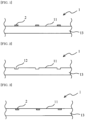
- a substrate 1 of the present invention includes a plurality of alkali metal azide spots 2 formed on a substantially flat surface 11.
- the substrate is also referred to as an "alkali metal azide spot-formed substrate”.
- a substrate prior to formation of alkali metal azide spots is also referred to as a "substrate member".
- the "substantially flat surface” of the substrate means a surface that does not have large irregularities that may serve as partition walls for separating a plurality of cells when the substrate is used to form a cell assembly.
- the “substantially flat surface” of the substrate may have slight irregularities that do not serve as the above partition walls.
- recesses 12 having a depth of 20% or less of the thickness of the substrate may be formed to be scattered in a spot-like pattern.
- the alkali metal azide spot-formed substrate 1 does not have an area that serves as partition walls for separating a plurality of cells when the substrate is used to form a cell assembly. Therefore, the alkali metal azide spot-formed substrate 1 has a high degree of flexibility in designing the size and shape of a unit cell produced and has high versatility.
- the alkali metal azide spot-formed substrate 1 does not have the above partition walls and hence can be produced without going through a complicated step of individually introducing a raw material as an alkali metal source into each of a plurality of separated cells. Therefore, if necessary, it is possible to easily produce the alkali metal azide spot-formed substrate 1.
- a material for the substrate member 13 is preferably a transparent material having optical transparency, and more preferably glass having heat resistance.
- the thickness of the substrate member 13 can be set appropriately, and is, for example, preferably 100 ⁇ m or more, and more preferably 500 ⁇ m or more from the viewpoint of strength, and is preferably 1.0 mm or less, and more preferably 0.8 mm or less from the viewpoint of light transmittance.
- the thickness of the substrate member 13 refers to the thickness of an area without the recesses 12.
- the alkali metal azide spots 2 are spots containing an alkali metal azide, and preferably spots composed of only an alkali metal azide.
- the alkali metal azide spots 2 composed of only an alkali metal azide are preferable because, when a gas cell is produced using the alkali metal azide spot-formed substrate 1, impurities that can adsorb a buffer gas are not generated in the cell. If a buffer gas in the cell is adsorbed to impurities, the internal pressure in the cell may change, which may result in a shift in the frequency of an electromagnetic wave absorbed by an alkali metal and a change in the temperature characteristics of an alkali metal.
- alkali metal azide examples include lithium azide, sodium azide, potassium azide, rubidium azide, and cesium azide. Among these, rubidium azide and cesium azide are preferred, and rubidium azide is more preferred.
- the transition frequency of rubidium atoms is lower than that of cesium atoms.
- alkali metal azides are stable substances at ordinary temperatures and ordinary pressures, the alkali metal azide spot-formed substrate 1 can be stored and transported at ordinary temperatures and ordinary pressures.
- the shape of the alkali metal azide spots 2 is not particularly limited, and may be, for example, circular, elliptical, or polygonal.
- the size of the alkali metal azide spots 2 can be set appropriately, but the circle-equivalent diameter of the alkali metal azide spots 2 is preferably 50 pm or more, more preferably 100 pm or more, and still more preferably 200 pm or more, and is preferably 2.0 mm or less, and more preferably 1.5 mm or less.
- the plurality of alkali metal azide spots 2 may have the same shape and size or different shapes and sizes, but preferably have the same shape and size. If the plurality of alkali metal azide spots 2 have the same shape and size, unit cells that are uniform in enclosed amount of the alkali metal can be easily produced using the alkali metal azide spot-formed substrate 1. More preferably, the plurality of the alkali metal azide spots 2 are formed as a uniform pattern.
- each of the alkali metal azide spots 2 may be formed in each of the recesses 12.
- the shape of the recesses 12 is not particularly limited, and may be, for example, a bowl, bottomed circular columnar, bottomed polygonal prismatic, inverted-conical, or inverted-polygonal pyramidal shape (a bottomed columnar shape in the illustrated example).
- the size of the recesses 12 can be set appropriately, but the outer diameter of the recesses 12 is, as a circle-equivalent diameter, for example, preferably 50 pm or more, more preferably 100 pm or more, and still more preferably 200 pm or more, and is preferably 2.0 mm or less, and more preferably 1.5 mm or less.
- the depth of the recesses 12 is preferably 1 pm or more, more preferably 10 pm or more, and still more preferably 20 pm or more from the viewpoint of reliably retaining the alkali metal azide-containing liquid in the recesses 12 in the formation of alkali metal azide spots 2 as described later; and is preferably 200 pm or less, more preferably 150 pm or less, and still more preferably 100 pm or less from the viewpoint of ensuring that the surface 11 is substantially flat.
- the ratio of the depth of the recesses 12 to the thickness of the substrate member 13 is preferably 0.1% or more, more preferably 1% or more, and still more preferably 10% or more, and is preferably 20% or less, more preferably 18% or less, and still more preferably 15% or less.
- the shape and size of the plurality of recesses 12 may be the same or different, but are preferably the same. If the shape and size of the plurality of recesses 12 are the same, the shape and size of the plurality of alkali metal azide spots 2 can be easily made the same, and unit cells that are uniform in enclosed amount of the alkali metal can be easily produced using the alkali metal azide spot-formed substrate 1.
- the substrate 1 having the plurality of alkali metal azide spots 2 formed on the substantially flat surface 11 can be produced by forming a coating formed from an alkali metal azide-containing liquid in a spot shape on the substrate member 13 having the substantially flat surface 11.
- alkali metal azide-containing liquid examples include a solution in which an alkali metal azide is dissolved and a dispersion liquid in which an alkali metal azide is dispersed.
- a solution in which an alkali metal azide is dissolved is preferred because it is easier to make the contents of an alkali metal azide in the plurality of alkali metal azide spots 2 more uniform.
- Examples of a solvent for the alkali metal azide-containing liquid include water, methanol, ethanol, isopropyl alcohol, acetonitrile, acetone, N-methylpyrrolidone, dimethyl sulfoxide, and N,N-dimethylformamide. Among these, water or methanol is preferred, and methanol is more preferred.
- the concentration of the alkali metal azide in the alkali metal azide-containing liquid is not particularly limited, and is, for example, preferably 0.5% by weight or more, and more preferably 1.0% by weight or more, and is preferably 15% by weight or less, and more preferably 10% by weight or less. If the concentration of the alkali metal azide is within the above range, a cell in which an alkali metal in an amount suitable for use in an atomic device is enclosed can be easily produced.
- the alkali metal azide-containing liquid As a method of forming the coating formed from the alkali metal azide-containing liquid in a spot shape on the substrate member 13, a method in which the alkali metal azide-containing liquid is dropped in appropriate amounts in a spot shape using an inkjet machine or dispenser can be given, but the following formation methods A, B and C are preferably given.
- the formation methods A, B, and C become enabled by the substrate member 13 having no large irregularities that may serve as partition walls for separating a plurality of cells when forming a cell assembly.
- the alkali metal azide spot-formed substrate 1 can be easily produced without a complicated process of individually introducing a raw material into each of a plurality of separated cells.
- the formation method A is a method in which a mask (mask layer) having holes scattered in a spot-like pattern is formed on the substantially flat surface 11 of the substrate member 13, the alkali metal azide-containing liquid is applied on the mask to form a coating, and then the mask is removed.
- the mask having holes scattered in a spot-like pattern is not particularly limited as long as it can be removed in a later step.
- the mask may be an adhesive tape with holes scattered in a spot-like pattern and may be a mask formed by generally called a lift-off method using a photoresist and a photomask.
- the application of the alkali metal azide-containing liquid in the formation method A may be performed using a coating machine such as a spin coater, and is performed so that a coating (that is, alkali metal azide spots 2) having a uniform thickness can be obtained after drying mentioned later.
- a coating that is, alkali metal azide spots 2 having a uniform thickness
- the dried coating has a uniform thickness, unit cells that are uniform in enclosed amount of an alkali metal can be easily produced using the alkali metal azide spot-formed substrate 1.
- the formation of the coating in the formation method A is performed by removing, in other words, drying the liquid component in the alkali metal azide-containing liquid.
- the drying method is not particularly limited, but drying by heating with hot air, a hot plate, or the like can be given.
- the removal of the mask in the formation method A can be performed by a suitable method selected according to the formed mask.
- a suitable method selected according to the formed mask For example, when an adhesive tape with holes scattered in a spot-like pattern is used to form the mask, the adhesive tape may be peeled off so that no adhesive remains.
- the formation method B is a method in which the alkali metal azide-containing liquid is applied on the substantially flat surface 11 of the substrate member 13 to form a coating, and then the coating is partially removed to leave the alkali metal azide in a spot-like pattern on the substantially flat surface 11.
- the application of the alkali metal azide-containing liquid and the formation of the coating in the formation method B are the same as the application of the alkali metal azide-containing liquid and the formation of the coating in the formation method A.
- etching method As a method of partially removing the coating and leaving the alkali metal azide in a spot-like pattern on the substantially flat surface 11, a method using a photoresist and a photomask, which is generally called an etching method, can be given.
- the formation method C is a method in which the alkali metal azide-containing liquid is applied on the substantially flat surface 11 of the substrate member 13 having a plurality of recesses 12 shown in FIG. 2 so as to remain only in the recesses 12 to form a coating in each of the recesses 12.
- the substrate member 13 used in the formation method C has a plurality of recesses 12 formed in advance on at least one side thereof.
- the method of forming the recesses 12 is not particularly limited, and any method that can form a plurality of uniform recesses 12 may be used. Examples thereof include a method of processing with an ultrashort pulse laser and a chemical etching method. Examples and preferred embodiments of the shape and size of the recesses 12 to be formed are the same as those described for the recesses 12 in the description on the substrate 1 mentioned above.
- the application of the alkali metal azide-containing liquid in the formation method C may be performed using a coating machine such as a spin coater, and is performed so that the alkali metal azide-containing liquid remains only in the recesses 12 of the substrate member 13.
- a coating machine such as a spin coater
- a rotary centrifugal force of the spin coater may be used to remove excess liquid other than the liquid in the recesses 12, or the substrate member 13 coated with the alkali metal azide-containing liquid may be tilted obliquely or turned vertically to remove excess liquid other than the liquid in the recesses 12.
- the formation of a mask prior to formation of the coating and the step of partially removing the formed coating are not necessary.
- the formation of the coating in the formation method C is the same as the formation of the coating in the formation method A.
- the method for producing a unit cell 7 shown in FIG. 5 includes steps of assembling a cell assembly 5 to laminate a partition layer 3 by which the alkali metal azide spots 2 are separated and a second substrate 4 facing the alkali metal azide spot-formed substrate 1 with the partition layer 3 interposed therebetween as shown in FIG. 4 , vaporizing the alkali metal azide by irradiating the cell assembly 5 with ultraviolet rays, and then cutting out a unit cell from the cell assembly 5.
- a conventional substrate which has partition walls for separating cells and on which an alkali metal raw material is placed has a low degree of flexibility in designing a unit cell.
- the shape of the partition layer 3 can be appropriately designed according to the use of a cell, and therefore, the unit cell 7 having any desired size and shape can be produced.
- the cell assembly 5 is a laminate structure in which the alkali metal azide spot-formed substrate 1 and the second substrate 4 are bonded via the partition layer 3. By sealing through holes 31 of the partition layer 3 with the alkali metal azide spot-formed substrate 1 and the second substrate 4, internal spaces 6 of the cells are formed as airtight spaces.
- the partition layer 3 serves to separate the alkali metal azide spots 2 and is a plate-like member having a plurality of through holes 31 in the thickness direction.
- a material for the partition layer 3 is not particularly limited, and examples thereof include glass, metals, resins, and silicones. Glass and silicones, which are suitable for microfabrication by etching or the like, are preferable, and silicones are more preferable.
- a thickness "a" (see FIG. 4 ) of the partition layer 3 can be appropriately set, but is preferably 0.1 mm or more, and more preferably 0.3 mm or more, and is preferably 5.0 mm or less, and more preferably 3.0 mm or less.
- the through holes 31 of the partition layer 3 can be formed by performing microfabrication by etching, blasting treatment, or the like.
- the size and shape of the through holes 31 can be appropriately set as long as the partition layer 3 and the alkali metal azide spots 2 of the alkali metal azide spot-formed substrate 1 do not overlap when the cell assembly 5 is assembled. Therefore, the unit cell 7 produced can have a desired size and shape according to the use of the cell.
- a material for the second substrate 4 is preferably a transparent member having optical transparency, and more preferably glass having heat resistance.
- the thickness of the second substrate 4 can be set appropriately, but, for example, is preferably 80 ⁇ m or more, and more preferably 100 ⁇ m or more, and is preferably 1.0 mm or less, and more preferably 0.8 mm or less.
- the method of bonding the partition layer 3 to the alkali metal azide spot-formed substrate 1 and the second substrate 4 can be appropriately selected according to the materials thereof, and is not particularly limited. Examples of the method of bonding them include anodic bonding, direct bonding, and surface activated bonding. The anodic bonding is preferred because it allows easily airtight bonding.
- bonding of the partition layer 3 to the alkali metal azide spot-formed substrate 1 and the second substrate 4 is preferably performed under a vacuum condition such as in a vacuum chamber.
- a vacuum condition such as in a vacuum chamber.
- a buffer gas inside the cells, and it is preferable to perform bonding of the partition layer 3 to the alkali metal azide spot-formed substrate 1 and the second substrate 4 (especially, bonding to form the internal spaces 6 of the cells as airtight spaces) in a buffer gas atmosphere created by introducing a buffer gas under a vacuum condition.
- the buffer gas include inert gases such as nitrogen gas, neon gas, argon gas, and a mixed gas of nitrogen gas and argon gas.
- the order of bonding the partition layer 3 to the alkali metal azide spot-formed substrate 1 and the second substrate 4 is not particularly limited.
- the partition layer 3 may be bonded to the second substrate 4 and then bonded to the alkali metal azide spot-formed substrate 1, the partition layer 3 may be bonded to the alkali metal azide spot-formed substrate 1 and then bonded to the second substrate 4, or the partition layer 3 may be bonded to the alkali metal azide spot-formed substrate 1 and to the second substrate 4 at the same time.
- the alkali metal azide spots 2 of the alkali metal azide spot-formed substrate 1 and the through holes 31 of the partition layer 3 are aligned with each other such that the alkali metal azide is not present on the bonding faces.
- the cell assembly 5 is irradiated with energy rays such as ultraviolet rays to vaporize by decomposing (reducing) the alkali metal azide, thereby generating an alkali metal gas in the internal spaces 6 of the cells separated by the alkali metal azide spot-formed substrate 1, the partition layer 3, and the second substrate 4.
- energy rays such as ultraviolet rays to vaporize by decomposing (reducing) the alkali metal azide, thereby generating an alkali metal gas in the internal spaces 6 of the cells separated by the alkali metal azide spot-formed substrate 1, the partition layer 3, and the second substrate 4.
- nitrogen gas is also generated by the above decomposition, nitrogen gas is an inert gas and thus can be used as a buffer gas. Therefore, if the raw material of the alkali metal is an alkali metal azide, no impurities other than an alkali metal gas and nitrogen gas serving as a buffer gas are generated, and thus the possibility that the properties of the alkali metal in the cells will change can be reduced.
- the cell assembly 5 can be separated along the dashed lines X shown in FIG. 4 by blade dicing, laser dicing, water dicing, or the like to cut out the unit cell 7.
- the unit cell 7 produced as described above can be used in atomic devices such as atomic clocks and atomic magnetic sensors.
Landscapes
- Physics & Mathematics (AREA)
- General Physics & Mathematics (AREA)
- Engineering & Computer Science (AREA)
- Chemical & Material Sciences (AREA)
- Life Sciences & Earth Sciences (AREA)
- Chemical Kinetics & Catalysis (AREA)
- General Chemical & Material Sciences (AREA)
- Geochemistry & Mineralogy (AREA)
- Materials Engineering (AREA)
- Organic Chemistry (AREA)
- Plasma & Fusion (AREA)
- Thermal Sciences (AREA)
- Spectroscopy & Molecular Physics (AREA)
- Ecology (AREA)
- Apparatus Associated With Microorganisms And Enzymes (AREA)
Abstract
Description
- The present invention relates to a substrate, a method for producing the substrate, and a method for producing a unit cell using the substrate.
- A cell in which an atomic gas is sealed (hereinafter also referred to as a gas cell) is used in an atomic device such as a high-precision atomic clock based on the frequency of an electromagnetic wave absorbed by the atom, an atomic magnetic sensor which uses optical pumping of the atom, or the like. As a production method of such a gas cell, a method is known in which a cell container is produced by glass fusion bonding or blowing, an alkali metal gas and a buffer gas are blown into the container, and the gases are sealed by pinching off (Non-Patent
Documents 1 and 2). - However, the production methods disclosed in
Non-Patent Documents Documents 3 and 4). -
- Non-Patent Document 1: J. Gouloumet, B. Leuenberger, C. Schori, S. Grop, and R. Rochat, "Progress towards a compact and low-power miniaturized Rubidium Oscillator (mRO™)" IEEE/MTT-S International Microwave Symposium, 2020, p.876-879
- Non-Patent Document 2: H. Zhang, H. Herdian, A. T. Narayanan, A. Shirane, M. Suzuki, K. Harasaka, K. Adachi, S. Goka, S. Yanagimachi, and K. Okada, "ULPAC: A Miniatured Ultralow-power Atomic Clock" IEEE Journal Of Solid-State Circuits, 2019, 54(11), p.3135-3148
- Non-Patent Document 3: S. Karlen, J. Gobet, T. Overstolz, J. Haesler, and S. Lecomte, "Lifetime assessment of RbN3-filled MEMS atomic vapor cells with Al2O3 coating" Optics express, 2017, 25(3), p.2187-2194
- Non-Patent Document 4: L. Liew, J. Moreland, and V. Gerginov, "Waferlevel filling of microfabricated atomic vapor cells based on thin-film deposition and photolysis of cesium azide" Applied Physics Letters, 2007, 90(11), 114106
- In the production method of a gas cell disclosed in
Non-Patent Document 3, RbN3 aqueous solution is pipetted into the cavities of a substrate where partition walls are formed to separate multiple cells, followed by drying, and the cavities are then hermetically sealed by anodic bonding of glass to the openings. The size and shape of a gas cell are required to be designed according to an atomic device to be used, whereas, in the production method of a gas cell disclosed in Non-PatentDocument 3, the cell shape cannot be changed after dispensing the RbN3 aqueous solution to the cells, and thus such a gas cell has less versatility. - In the production method of a gas cell disclosed in Non-Patent Document 4, a CsN3 film is formed by vapor-phase film formation by vapor deposition in the cavities of a substrate where partition walls are formed to separate multiple cells, and the cavities are then hermetically sealed by anodic bonding of glass to the openings. However, even in the production method disclosed in Non-Patent Document 4, the cell shape cannot be changed after dispensing CsN3 to the cells, and thus such a gas cell has less versatility. In addition, in the above vapor deposition, explosion and bumping of CsN3 are likely to occur during heating, and the CsN3 film formed may be non-uniform. Thus, the enclosed amount of Cs was not quantitative, and uniform unit cells could not be obtained.
- The present invention has been made by focusing on the above situation, and an object of the present invention is to provide a substrate with high versatility, a method for producing the substrate, and a method for producing a unit cell using the substrate.
- The gist of the present invention is as follows.
- [1] A substrate comprising a plurality of alkali metal azide spots on a substantially flat surface.
- [2] The substrate according to [1], wherein the substrate comprises a plurality of recesses scattered in a spot-like pattern on the substantially flat surface, and each of the alkali metal azide spots is formed in each of the recesses.
- [3] A method for producing the substrate according to [1] or [2], wherein a coating formed from an alkali metal azide-containing liquid is formed in a spot shape on a substrate member.
- [4] The method according to [3], wherein a mask having holes scattered in a spot-like pattern is formed on the substrate member, the alkali metal azide-containing liquid is applied on the mask to form the coating, and then the mask is removed.
- [5] The method according to [3], wherein the alkali metal azide-containing liquid is applied to the substrate member to form the coating, and then the coating is partially removed to leave the alkali metal azide in a spot-like pattern on the substantially flat surface.
- [6] A method for producing the substrate according to [2], wherein an alkali metal azide-containing liquid is applied to a substrate member so as to remain only in the recesses to form a coating formed from the alkali metal azide-containing liquid in a spot shape in each of the recesses.
- [7] A method for producing a unit cell comprising the steps of:
- assembling a cell assembly to laminate, on the substrate according to [1] or [2], a partition layer by which the alkali metal azide spots are separated and a second substrate facing the substrate with the partition layer interposed therebetween,
- vaporizing the alkali metal azide by irradiating the cell assembly with ultraviolet rays, and
- then cutting out a unit cell from the cell assembly.
- [8] The method according to [7], wherein the step of assembling the cell assembly is performed under a vacuum condition in which a buffer gas may be introduced.
- According to the present invention, it is possible to provide a substrate with high versatility, a method for producing the substrate, and a method for producing a unit cell using the substrate. In addition, the substrate can be easily produced.
-
-
FIG. 1 is a schematic cross-sectional view showing an example of a substrate according to an embodiment of the present invention. -
FIG. 2 is a schematic cross-sectional view showing an example of a member used in a production step of a substrate shown inFIG. 3 . -
FIG. 3 is a schematic cross-sectional view showing another example of a substrate according to an embodiment of the present invention. -
FIG. 4 is a schematic cross-sectional view showing an example of a step of assembling a cell assembly in a method for producing a unit cell according to an embodiment of the present invention. -
FIG. 5 is a schematic cross-sectional view showing an example of a unit cell obtained by a method for producing a unit cell according to an embodiment of the present invention. - Hereinafter, a substrate, a method for producing the substrate, and a method for producing a unit cell using the substrate according to the present invention will be specifically described with reference to the drawings as necessary. The present invention, however, is not limited by the following examples shown in the drawings but can also be absolutely carried out with appropriate changes to the examples within a scope in compliance with the intent of the present invention, and all the changes are to be encompassed within a technical scope of the present invention.
- As shown in
FIG. 1 and FIG. 3 , asubstrate 1 of the present invention includes a plurality of alkalimetal azide spots 2 formed on a substantiallyflat surface 11. In the following, the substrate is also referred to as an "alkali metal azide spot-formed substrate". A substrate prior to formation of alkali metal azide spots is also referred to as a "substrate member". In the present invention, the "substantially flat surface" of the substrate means a surface that does not have large irregularities that may serve as partition walls for separating a plurality of cells when the substrate is used to form a cell assembly. The "substantially flat surface" of the substrate may have slight irregularities that do not serve as the above partition walls. Specifically,recesses 12 having a depth of 20% or less of the thickness of the substrate may be formed to be scattered in a spot-like pattern. The alkali metal azide spot-formedsubstrate 1 does not have an area that serves as partition walls for separating a plurality of cells when the substrate is used to form a cell assembly. Therefore, the alkali metal azide spot-formedsubstrate 1 has a high degree of flexibility in designing the size and shape of a unit cell produced and has high versatility. In addition, the alkali metal azide spot-formedsubstrate 1 does not have the above partition walls and hence can be produced without going through a complicated step of individually introducing a raw material as an alkali metal source into each of a plurality of separated cells. Therefore, if necessary, it is possible to easily produce the alkali metal azide spot-formedsubstrate 1. - Since application examples of a gas cell using the alkali metal azide spot-formed
substrate 1 include an atomic clock, an atomic magnetic sensor, and a quantum gyro, which utilize laser spectroscopy, a material for thesubstrate member 13 is preferably a transparent material having optical transparency, and more preferably glass having heat resistance. - The thickness of the
substrate member 13 can be set appropriately, and is, for example, preferably 100 µm or more, and more preferably 500 µm or more from the viewpoint of strength, and is preferably 1.0 mm or less, and more preferably 0.8 mm or less from the viewpoint of light transmittance. When thesubstrate member 13 has therecesses 12, the thickness of thesubstrate member 13 refers to the thickness of an area without therecesses 12. - The alkali
metal azide spots 2 are spots containing an alkali metal azide, and preferably spots composed of only an alkali metal azide. The alkalimetal azide spots 2 composed of only an alkali metal azide are preferable because, when a gas cell is produced using the alkali metal azide spot-formedsubstrate 1, impurities that can adsorb a buffer gas are not generated in the cell. If a buffer gas in the cell is adsorbed to impurities, the internal pressure in the cell may change, which may result in a shift in the frequency of an electromagnetic wave absorbed by an alkali metal and a change in the temperature characteristics of an alkali metal. - Examples of the alkali metal azide include lithium azide, sodium azide, potassium azide, rubidium azide, and cesium azide. Among these, rubidium azide and cesium azide are preferred, and rubidium azide is more preferred. The transition frequency of rubidium atoms is lower than that of cesium atoms. When a gas cell using the alkali metal azide spot-formed
substrate 1 is used in an atomic clock or the like, if the alkali metal azide is rubidium azide, the power consumption of the electronic circuit can be kept low. - Since alkali metal azides are stable substances at ordinary temperatures and ordinary pressures, the alkali metal azide spot-formed
substrate 1 can be stored and transported at ordinary temperatures and ordinary pressures. - The shape of the alkali
metal azide spots 2 is not particularly limited, and may be, for example, circular, elliptical, or polygonal. The size of the alkalimetal azide spots 2 can be set appropriately, but the circle-equivalent diameter of the alkalimetal azide spots 2 is preferably 50 pm or more, more preferably 100 pm or more, and still more preferably 200 pm or more, and is preferably 2.0 mm or less, and more preferably 1.5 mm or less. - The plurality of alkali
metal azide spots 2 may have the same shape and size or different shapes and sizes, but preferably have the same shape and size. If the plurality of alkalimetal azide spots 2 have the same shape and size, unit cells that are uniform in enclosed amount of the alkali metal can be easily produced using the alkali metal azide spot-formedsubstrate 1. More preferably, the plurality of the alkalimetal azide spots 2 are formed as a uniform pattern. - When the
substrate member 13 has a plurality ofrecesses 12 scattered in a spot-like pattern on the substantiallyflat surface 11, each of the alkalimetal azide spots 2 may be formed in each of therecesses 12. - The shape of the
recesses 12 is not particularly limited, and may be, for example, a bowl, bottomed circular columnar, bottomed polygonal prismatic, inverted-conical, or inverted-polygonal pyramidal shape (a bottomed columnar shape in the illustrated example). The size of therecesses 12 can be set appropriately, but the outer diameter of therecesses 12 is, as a circle-equivalent diameter, for example, preferably 50 pm or more, more preferably 100 pm or more, and still more preferably 200 pm or more, and is preferably 2.0 mm or less, and more preferably 1.5 mm or less. The depth of therecesses 12 is preferably 1 pm or more, more preferably 10 pm or more, and still more preferably 20 pm or more from the viewpoint of reliably retaining the alkali metal azide-containing liquid in therecesses 12 in the formation of alkalimetal azide spots 2 as described later; and is preferably 200 pm or less, more preferably 150 pm or less, and still more preferably 100 pm or less from the viewpoint of ensuring that thesurface 11 is substantially flat. The ratio of the depth of therecesses 12 to the thickness of thesubstrate member 13 is preferably 0.1% or more, more preferably 1% or more, and still more preferably 10% or more, and is preferably 20% or less, more preferably 18% or less, and still more preferably 15% or less. - The shape and size of the plurality of
recesses 12 may be the same or different, but are preferably the same. If the shape and size of the plurality ofrecesses 12 are the same, the shape and size of the plurality of alkalimetal azide spots 2 can be easily made the same, and unit cells that are uniform in enclosed amount of the alkali metal can be easily produced using the alkali metal azide spot-formedsubstrate 1. - The
substrate 1 having the plurality of alkalimetal azide spots 2 formed on the substantially flat surface 11 (alkali metal azide spot-formed substrate) can be produced by forming a coating formed from an alkali metal azide-containing liquid in a spot shape on thesubstrate member 13 having the substantiallyflat surface 11. - Examples of the alkali metal azide-containing liquid include a solution in which an alkali metal azide is dissolved and a dispersion liquid in which an alkali metal azide is dispersed. A solution in which an alkali metal azide is dissolved is preferred because it is easier to make the contents of an alkali metal azide in the plurality of alkali
metal azide spots 2 more uniform. - Examples of a solvent for the alkali metal azide-containing liquid include water, methanol, ethanol, isopropyl alcohol, acetonitrile, acetone, N-methylpyrrolidone, dimethyl sulfoxide, and N,N-dimethylformamide. Among these, water or methanol is preferred, and methanol is more preferred.
- The concentration of the alkali metal azide in the alkali metal azide-containing liquid is not particularly limited, and is, for example, preferably 0.5% by weight or more, and more preferably 1.0% by weight or more, and is preferably 15% by weight or less, and more preferably 10% by weight or less. If the concentration of the alkali metal azide is within the above range, a cell in which an alkali metal in an amount suitable for use in an atomic device is enclosed can be easily produced.
- As a method of forming the coating formed from the alkali metal azide-containing liquid in a spot shape on the
substrate member 13, a method in which the alkali metal azide-containing liquid is dropped in appropriate amounts in a spot shape using an inkjet machine or dispenser can be given, but the following formation methods A, B and C are preferably given. The formation methods A, B, and C become enabled by thesubstrate member 13 having no large irregularities that may serve as partition walls for separating a plurality of cells when forming a cell assembly. By the formation methods A, B, and C, the alkali metal azide spot-formedsubstrate 1 can be easily produced without a complicated process of individually introducing a raw material into each of a plurality of separated cells. - The formation method A is a method in which a mask (mask layer) having holes scattered in a spot-like pattern is formed on the substantially
flat surface 11 of thesubstrate member 13, the alkali metal azide-containing liquid is applied on the mask to form a coating, and then the mask is removed. - In the formation method A, the mask having holes scattered in a spot-like pattern is not particularly limited as long as it can be removed in a later step. The mask may be an adhesive tape with holes scattered in a spot-like pattern and may be a mask formed by generally called a lift-off method using a photoresist and a photomask.
- The application of the alkali metal azide-containing liquid in the formation method A may be performed using a coating machine such as a spin coater, and is performed so that a coating (that is, alkali metal azide spots 2) having a uniform thickness can be obtained after drying mentioned later. When the dried coating has a uniform thickness, unit cells that are uniform in enclosed amount of an alkali metal can be easily produced using the alkali metal azide spot-formed
substrate 1. - The formation of the coating in the formation method A is performed by removing, in other words, drying the liquid component in the alkali metal azide-containing liquid. The drying method is not particularly limited, but drying by heating with hot air, a hot plate, or the like can be given.
- The removal of the mask in the formation method A can be performed by a suitable method selected according to the formed mask. For example, when an adhesive tape with holes scattered in a spot-like pattern is used to form the mask, the adhesive tape may be peeled off so that no adhesive remains.
- The formation method B is a method in which the alkali metal azide-containing liquid is applied on the substantially
flat surface 11 of thesubstrate member 13 to form a coating, and then the coating is partially removed to leave the alkali metal azide in a spot-like pattern on the substantiallyflat surface 11. - The application of the alkali metal azide-containing liquid and the formation of the coating in the formation method B are the same as the application of the alkali metal azide-containing liquid and the formation of the coating in the formation method A.
- In the formation method B, as a method of partially removing the coating and leaving the alkali metal azide in a spot-like pattern on the substantially
flat surface 11, a method using a photoresist and a photomask, which is generally called an etching method, can be given. - The formation method C is a method in which the alkali metal azide-containing liquid is applied on the substantially
flat surface 11 of thesubstrate member 13 having a plurality ofrecesses 12 shown inFIG. 2 so as to remain only in therecesses 12 to form a coating in each of therecesses 12. - The
substrate member 13 used in the formation method C has a plurality ofrecesses 12 formed in advance on at least one side thereof. The method of forming therecesses 12 is not particularly limited, and any method that can form a plurality ofuniform recesses 12 may be used. Examples thereof include a method of processing with an ultrashort pulse laser and a chemical etching method. Examples and preferred embodiments of the shape and size of therecesses 12 to be formed are the same as those described for therecesses 12 in the description on thesubstrate 1 mentioned above. - The application of the alkali metal azide-containing liquid in the formation method C may be performed using a coating machine such as a spin coater, and is performed so that the alkali metal azide-containing liquid remains only in the
recesses 12 of thesubstrate member 13. As a method of leaving the alkali metal azide-containing liquid only in therecesses 12 of thesubstrate member 13, for example, when a spin coater is used for the application, a rotary centrifugal force of the spin coater may be used to remove excess liquid other than the liquid in therecesses 12, or thesubstrate member 13 coated with the alkali metal azide-containing liquid may be tilted obliquely or turned vertically to remove excess liquid other than the liquid in therecesses 12. - When the
substrate member 13 has the plurality ofrecesses 12, the formation of a mask prior to formation of the coating and the step of partially removing the formed coating are not necessary. - The formation of the coating in the formation method C is the same as the formation of the coating in the formation method A.
- The method for producing a
unit cell 7 shown inFIG. 5 includes steps of assembling acell assembly 5 to laminate apartition layer 3 by which the alkalimetal azide spots 2 are separated and a second substrate 4 facing the alkali metal azide spot-formedsubstrate 1 with thepartition layer 3 interposed therebetween as shown inFIG. 4 , vaporizing the alkali metal azide by irradiating thecell assembly 5 with ultraviolet rays, and then cutting out a unit cell from thecell assembly 5. A conventional substrate which has partition walls for separating cells and on which an alkali metal raw material is placed has a low degree of flexibility in designing a unit cell. However, by using the alkali metal azide spot-formedsubstrate 1, the shape of thepartition layer 3 can be appropriately designed according to the use of a cell, and therefore, theunit cell 7 having any desired size and shape can be produced. - The
cell assembly 5 is a laminate structure in which the alkali metal azide spot-formedsubstrate 1 and the second substrate 4 are bonded via thepartition layer 3. By sealing through holes 31 of thepartition layer 3 with the alkali metal azide spot-formedsubstrate 1 and the second substrate 4,internal spaces 6 of the cells are formed as airtight spaces. - The
partition layer 3 serves to separate the alkalimetal azide spots 2 and is a plate-like member having a plurality of through holes 31 in the thickness direction. - A material for the
partition layer 3 is not particularly limited, and examples thereof include glass, metals, resins, and silicones. Glass and silicones, which are suitable for microfabrication by etching or the like, are preferable, and silicones are more preferable. - A thickness "a" (see
FIG. 4 ) of thepartition layer 3 can be appropriately set, but is preferably 0.1 mm or more, and more preferably 0.3 mm or more, and is preferably 5.0 mm or less, and more preferably 3.0 mm or less. - The through holes 31 of the
partition layer 3 can be formed by performing microfabrication by etching, blasting treatment, or the like. The size and shape of the through holes 31 can be appropriately set as long as thepartition layer 3 and the alkalimetal azide spots 2 of the alkali metal azide spot-formedsubstrate 1 do not overlap when thecell assembly 5 is assembled. Therefore, theunit cell 7 produced can have a desired size and shape according to the use of the cell. - Since a cell using the second substrate 4 is used in atomic clocks, atomic magnetic sensors, and the like, a material for the second substrate 4 is preferably a transparent member having optical transparency, and more preferably glass having heat resistance.
- The thickness of the second substrate 4 can be set appropriately, but, for example, is preferably 80 µm or more, and more preferably 100 µm or more, and is preferably 1.0 mm or less, and more preferably 0.8 mm or less.
- The method of bonding the
partition layer 3 to the alkali metal azide spot-formedsubstrate 1 and the second substrate 4 can be appropriately selected according to the materials thereof, and is not particularly limited. Examples of the method of bonding them include anodic bonding, direct bonding, and surface activated bonding. The anodic bonding is preferred because it allows easily airtight bonding. - Since an elemental alkali metal is oxidized in a short time in the presence of oxygen and moisture, bonding of the
partition layer 3 to the alkali metal azide spot-formedsubstrate 1 and the second substrate 4 (especially, bonding to form theinternal spaces 6 of the cells as airtight spaces) is preferably performed under a vacuum condition such as in a vacuum chamber. When an elemental alkali metal in the cell collides with the inner wall of the cell, the internal state of the alkali metal atom may change. Therefore, it is preferable to enclose a buffer gas inside the cells, and it is preferable to perform bonding of thepartition layer 3 to the alkali metal azide spot-formedsubstrate 1 and the second substrate 4 (especially, bonding to form theinternal spaces 6 of the cells as airtight spaces) in a buffer gas atmosphere created by introducing a buffer gas under a vacuum condition. Examples of the buffer gas include inert gases such as nitrogen gas, neon gas, argon gas, and a mixed gas of nitrogen gas and argon gas. - The order of bonding the
partition layer 3 to the alkali metal azide spot-formedsubstrate 1 and the second substrate 4 is not particularly limited. Thepartition layer 3 may be bonded to the second substrate 4 and then bonded to the alkali metal azide spot-formedsubstrate 1, thepartition layer 3 may be bonded to the alkali metal azide spot-formedsubstrate 1 and then bonded to the second substrate 4, or thepartition layer 3 may be bonded to the alkali metal azide spot-formedsubstrate 1 and to the second substrate 4 at the same time. When thepartition layer 3 is bonded to the alkali metal azide spot-formedsubstrate 1, the alkalimetal azide spots 2 of the alkali metal azide spot-formedsubstrate 1 and the through holes 31 of thepartition layer 3 are aligned with each other such that the alkali metal azide is not present on the bonding faces. By making the number of the alkalimetal azide spots 2 accommodated in the through holes 31 of thepartition layer 3 the same between the through holes 31,unit cells 7 that are uniform in enclosed amount of an alkali metal can be produced. - The
cell assembly 5 is irradiated with energy rays such as ultraviolet rays to vaporize by decomposing (reducing) the alkali metal azide, thereby generating an alkali metal gas in theinternal spaces 6 of the cells separated by the alkali metal azide spot-formedsubstrate 1, thepartition layer 3, and the second substrate 4. Although nitrogen gas is also generated by the above decomposition, nitrogen gas is an inert gas and thus can be used as a buffer gas. Therefore, if the raw material of the alkali metal is an alkali metal azide, no impurities other than an alkali metal gas and nitrogen gas serving as a buffer gas are generated, and thus the possibility that the properties of the alkali metal in the cells will change can be reduced. - The
cell assembly 5 can be separated along the dashed lines X shown inFIG. 4 by blade dicing, laser dicing, water dicing, or the like to cut out theunit cell 7. - The
unit cell 7 produced as described above can be used in atomic devices such as atomic clocks and atomic magnetic sensors. - The present application claims priority based on
Japanese Patent Application No. 2021-039388 filed on March 11, 2021 Japanese Patent Application No. 2021-039388 filed on March 11, 2021 -
- 1: substrate (alkali metal azide spot-formed substrate)
- 11: substantially flat surface
- 12: recess
- 13: substrate member
- 2: alkali metal azide spot
- 3: partition layer
- 31: through hole
- 4: second substrate
- 5: cell assembly
- 6: internal space of cell
- 7: unit cell
- a: thickness of partition layer
Claims (8)
- A substrate comprising a plurality of alkali metal azide spots on a substantially flat surface.
- The substrate according to claim 1, wherein the substrate comprises a plurality of recesses scattered in a spot-like pattern on the substantially flat surface, and each of the alkali metal azide spots is formed in each of the recesses.
- A method for producing the substrate according to claim 1 or 2, wherein a coating formed from an alkali metal azide-containing liquid is formed in a spot shape on a substrate member.
- The method according to claim 3, wherein a mask having holes scattered in a spot-like pattern is formed on the substrate member, the alkali metal azide-containing liquid is applied on the mask to form the coating, and then the mask is removed.
- The method according to claim 3, wherein the alkali metal azide-containing liquid is applied to the substrate member to form the coating, and then the coating is partially removed to leave the alkali metal azide in a spot-like pattern on the substantially flat surface.
- A method for producing the substrate according to claim 2, wherein an alkali metal azide-containing liquid is applied to a substrate member so as to remain only in the recesses to form a coating formed from the alkali metal azide-containing liquid in a spot shape in each of the recesses.
- A method for producing a unit cell comprising the steps of:assembling a cell assembly to laminate, on the substrate according to claim 1 or 2, a partition layer by which the alkali metal azide spots are separated and a second substrate facing the substrate with the partition layer interposed therebetween,vaporizing the alkali metal azide by irradiating the cell assembly with ultraviolet rays, andthen cutting out a unit cell from the cell assembly.
- The method according to claim 7, wherein the step of assembling the cell assembly is performed under a vacuum condition in which a buffer gas may be introduced.
Applications Claiming Priority (2)
| Application Number | Priority Date | Filing Date | Title |
|---|---|---|---|
| JP2021039388 | 2021-03-11 | ||
| PCT/JP2022/003180 WO2022190694A1 (en) | 2021-03-11 | 2022-01-27 | Substrate, production method for substrate, and production method for unit cell |
Publications (2)
| Publication Number | Publication Date |
|---|---|
| EP4307565A1 true EP4307565A1 (en) | 2024-01-17 |
| EP4307565A4 EP4307565A4 (en) | 2025-03-19 |
Family
ID=83226650
Family Applications (1)
| Application Number | Title | Priority Date | Filing Date |
|---|---|---|---|
| EP22766661.7A Pending EP4307565A4 (en) | 2021-03-11 | 2022-01-27 | Substrate, production method for substrate, and production method for unit cell |
Country Status (4)
| Country | Link |
|---|---|
| US (1) | US12617713B2 (en) |
| EP (1) | EP4307565A4 (en) |
| JP (1) | JP7730513B2 (en) |
| WO (1) | WO2022190694A1 (en) |
Family Cites Families (10)
| Publication number | Priority date | Publication date | Assignee | Title |
|---|---|---|---|---|
| JP5699725B2 (en) * | 2011-03-23 | 2015-04-15 | セイコーエプソン株式会社 | Gas cell manufacturing apparatus and gas cell manufacturing method |
| US9310447B2 (en) | 2011-11-18 | 2016-04-12 | Hitachi, Ltd. | Magnetic field measuring apparatus and method for manufacturing same |
| JP6248572B2 (en) * | 2012-11-21 | 2017-12-20 | 株式会社リコー | Method for producing alkali metal cell and method for producing atomic oscillator |
| JP2016029699A (en) | 2014-07-18 | 2016-03-03 | 株式会社リコー | Method of manufacturing substrate, method of manufacturing alkali metal cell, composite substrate, method of manufacturing composite substrate, and alkali metal cell |
| JP2016092465A (en) | 2014-10-30 | 2016-05-23 | セイコーエプソン株式会社 | Atomic cell manufacturing method, atomic cell, quantum interference device, atomic oscillator, electronic device, and moving body |
| JP2016207695A (en) | 2015-04-15 | 2016-12-08 | セイコーエプソン株式会社 | Atomic cell, method for manufacturing atomic cell, quantum interference device, atomic oscillator, electronic apparatus and mobile body |
| JP2017098373A (en) * | 2015-11-20 | 2017-06-01 | 株式会社リコー | Gas cell, gas cell manufacturing method, and atomic oscillator |
| JP6696589B2 (en) * | 2016-11-22 | 2020-05-20 | 株式会社村田製作所 | Atomic oscillator and electronic equipment |
| JP2021039388A (en) | 2017-12-26 | 2021-03-11 | パナソニックIpマネジメント株式会社 | Positioning device and vehicle |
| US11180844B2 (en) * | 2018-07-02 | 2021-11-23 | Government Of The United States Of America, As Represented By The Secretary Of Commerce | Process for making alkali metal vapor cells |
-
2022
- 2022-01-27 WO PCT/JP2022/003180 patent/WO2022190694A1/en not_active Ceased
- 2022-01-27 EP EP22766661.7A patent/EP4307565A4/en active Pending
- 2022-01-27 US US18/280,747 patent/US12617713B2/en active Active
- 2022-01-27 JP JP2023505195A patent/JP7730513B2/en active Active
Also Published As
| Publication number | Publication date |
|---|---|
| US12617713B2 (en) | 2026-05-05 |
| WO2022190694A1 (en) | 2022-09-15 |
| JPWO2022190694A1 (en) | 2022-09-15 |
| US20240150229A1 (en) | 2024-05-09 |
| EP4307565A4 (en) | 2025-03-19 |
| JP7730513B2 (en) | 2025-08-28 |
Similar Documents
| Publication | Publication Date | Title |
|---|---|---|
| US8906470B2 (en) | Method for producing a microfabricated atomic vapor cell | |
| CN104188626B (en) | Production method of gas cell, and gas cell, production method of magnetic measurement device and magnetic measurement device | |
| Liew et al. | Wafer-level filling of microfabricated atomic vapor cells based on thin-film deposition and photolysis of cesium azide | |
| Straessle et al. | Microfabricated alkali vapor cell with anti-relaxation wall coating | |
| Liew et al. | Microfabricated alkali atom vapor cells | |
| JP5961998B2 (en) | Method for manufacturing atomic oscillator | |
| US9498777B2 (en) | Cells having cavities and the manufacture and use of the same | |
| US20050007118A1 (en) | Micromachined alkali-atom vapor cells and method of fabrication | |
| JP6572528B2 (en) | Method for manufacturing atomic cell | |
| JP2016207695A (en) | Atomic cell, method for manufacturing atomic cell, quantum interference device, atomic oscillator, electronic apparatus and mobile body | |
| CN107850870A (en) | Gas cell suitable for atomic sensor and method of filling gas cell | |
| US7666485B2 (en) | Alkali metal-wax micropackets for alkali metal handling | |
| Bashir et al. | Plasma polymerization in a microcapillary using an atmospheric pressure dielectric barrier discharge | |
| JP7821810B2 (en) | Method for sealing a reference gas in a MEMS cell | |
| US12617713B2 (en) | Substrate, method for producing substrate, and method for producing unit cell | |
| JP6217261B2 (en) | Method for manufacturing atomic cell | |
| JP6179277B2 (en) | Method for producing alkali metal cell and method for producing atomic oscillator | |
| JP6036230B2 (en) | Method for producing alkali metal cell and method for producing atomic oscillator | |
| Liew et al. | Micromachined alkali atom vapor cells for chip-scale atomic clocks | |
| Kiyose et al. | Microfabricated alkali metal vapor cells filled with an on-chip dispensing component | |
| US7229669B2 (en) | Thin-film deposition methods and apparatuses | |
| US11899406B2 (en) | Devices, systems, and methods for fabricating alkali vapor cells | |
| JP6447678B2 (en) | Atomic cell manufacturing method, atomic cell, quantum interference device, atomic oscillator, and electronic device | |
| JP7780803B2 (en) | Metal gas filled cell and its manufacturing method | |
| Hirai et al. | Low temperature, wafer-level process of alkali-metal vapor cells for micro-fabricated atomic clocks |
Legal Events
| Date | Code | Title | Description |
|---|---|---|---|
| STAA | Information on the status of an ep patent application or granted ep patent |
Free format text: STATUS: THE INTERNATIONAL PUBLICATION HAS BEEN MADE |
|
| PUAI | Public reference made under article 153(3) epc to a published international application that has entered the european phase |
Free format text: ORIGINAL CODE: 0009012 |
|
| STAA | Information on the status of an ep patent application or granted ep patent |
Free format text: STATUS: REQUEST FOR EXAMINATION WAS MADE |
|
| 17P | Request for examination filed |
Effective date: 20230914 |
|
| AK | Designated contracting states |
Kind code of ref document: A1 Designated state(s): AL AT BE BG CH CY CZ DE DK EE ES FI FR GB GR HR HU IE IS IT LI LT LU LV MC MK MT NL NO PL PT RO RS SE SI SK SM TR |
|
| DAV | Request for validation of the european patent (deleted) | ||
| DAX | Request for extension of the european patent (deleted) | ||
| A4 | Supplementary search report drawn up and despatched |
Effective date: 20250219 |
|
| RIC1 | Information provided on ipc code assigned before grant |
Ipc: B82Y 20/00 20110101ALI20250213BHEP Ipc: B82B 1/00 20060101ALI20250213BHEP Ipc: G01N 21/11 20060101ALI20250213BHEP Ipc: G01N 21/03 20060101ALI20250213BHEP Ipc: H01J 65/04 20060101ALI20250213BHEP Ipc: G04F 5/14 20060101ALI20250213BHEP Ipc: G01C 19/62 20060101ALI20250213BHEP Ipc: H01S 1/06 20060101ALI20250213BHEP Ipc: H03L 7/26 20060101AFI20250213BHEP |