EP4307544A1 - Power supply device - Google Patents
Power supply device Download PDFInfo
- Publication number
- EP4307544A1 EP4307544A1 EP22766864.7A EP22766864A EP4307544A1 EP 4307544 A1 EP4307544 A1 EP 4307544A1 EP 22766864 A EP22766864 A EP 22766864A EP 4307544 A1 EP4307544 A1 EP 4307544A1
- Authority
- EP
- European Patent Office
- Prior art keywords
- voltage
- power supply
- circuit
- bus
- supply apparatus
- Prior art date
- Legal status (The legal status is an assumption and is not a legal conclusion. Google has not performed a legal analysis and makes no representation as to the accuracy of the status listed.)
- Pending
Links
- 230000001172 regenerating effect Effects 0.000 description 30
- 230000008929 regeneration Effects 0.000 description 20
- 238000011069 regeneration method Methods 0.000 description 20
- 238000010586 diagram Methods 0.000 description 14
- 239000003990 capacitor Substances 0.000 description 9
- 101100464779 Saccharomyces cerevisiae (strain ATCC 204508 / S288c) CNA1 gene Proteins 0.000 description 5
- 101100464782 Saccharomyces cerevisiae (strain ATCC 204508 / S288c) CMP2 gene Proteins 0.000 description 4
- 230000000694 effects Effects 0.000 description 3
- 238000004804 winding Methods 0.000 description 3
- 238000013459 approach Methods 0.000 description 2
- 230000005669 field effect Effects 0.000 description 1
- 238000012986 modification Methods 0.000 description 1
- 230000004048 modification Effects 0.000 description 1
- 230000007704 transition Effects 0.000 description 1
Images





Classifications
-
- H—ELECTRICITY
- H02—GENERATION; CONVERSION OR DISTRIBUTION OF ELECTRIC POWER
- H02M—APPARATUS FOR CONVERSION BETWEEN AC AND AC, BETWEEN AC AND DC, OR BETWEEN DC AND DC, AND FOR USE WITH MAINS OR SIMILAR POWER SUPPLY SYSTEMS; CONVERSION OF DC OR AC INPUT POWER INTO SURGE OUTPUT POWER; CONTROL OR REGULATION THEREOF
- H02M1/00—Details of apparatus for conversion
- H02M1/32—Means for protecting converters other than automatic disconnection
-
- H—ELECTRICITY
- H02—GENERATION; CONVERSION OR DISTRIBUTION OF ELECTRIC POWER
- H02H—EMERGENCY PROTECTIVE CIRCUIT ARRANGEMENTS
- H02H9/00—Emergency protective circuit arrangements for limiting excess current or voltage without disconnection
- H02H9/04—Emergency protective circuit arrangements for limiting excess current or voltage without disconnection responsive to excess voltage
- H02H9/041—Emergency protective circuit arrangements for limiting excess current or voltage without disconnection responsive to excess voltage using a short-circuiting device
-
- H—ELECTRICITY
- H02—GENERATION; CONVERSION OR DISTRIBUTION OF ELECTRIC POWER
- H02M—APPARATUS FOR CONVERSION BETWEEN AC AND AC, BETWEEN AC AND DC, OR BETWEEN DC AND DC, AND FOR USE WITH MAINS OR SIMILAR POWER SUPPLY SYSTEMS; CONVERSION OF DC OR AC INPUT POWER INTO SURGE OUTPUT POWER; CONTROL OR REGULATION THEREOF
- H02M1/00—Details of apparatus for conversion
- H02M1/32—Means for protecting converters other than automatic disconnection
- H02M1/322—Means for rapidly discharging a capacitor of the converter for protecting electrical components or for preventing electrical shock
-
- H—ELECTRICITY
- H02—GENERATION; CONVERSION OR DISTRIBUTION OF ELECTRIC POWER
- H02M—APPARATUS FOR CONVERSION BETWEEN AC AND AC, BETWEEN AC AND DC, OR BETWEEN DC AND DC, AND FOR USE WITH MAINS OR SIMILAR POWER SUPPLY SYSTEMS; CONVERSION OF DC OR AC INPUT POWER INTO SURGE OUTPUT POWER; CONTROL OR REGULATION THEREOF
- H02M3/00—Conversion of DC power input into DC power output
- H02M3/22—Conversion of DC power input into DC power output with intermediate conversion into AC
- H02M3/24—Conversion of DC power input into DC power output with intermediate conversion into AC by static converters
- H02M3/28—Conversion of DC power input into DC power output with intermediate conversion into AC by static converters using discharge tubes with control electrode or semiconductor devices with control electrode to produce the intermediate AC
- H02M3/325—Conversion of DC power input into DC power output with intermediate conversion into AC by static converters using discharge tubes with control electrode or semiconductor devices with control electrode to produce the intermediate AC using devices of a triode or a transistor type requiring continuous application of a control signal
- H02M3/335—Conversion of DC power input into DC power output with intermediate conversion into AC by static converters using discharge tubes with control electrode or semiconductor devices with control electrode to produce the intermediate AC using devices of a triode or a transistor type requiring continuous application of a control signal using semiconductor devices only
- H02M3/33507—Conversion of DC power input into DC power output with intermediate conversion into AC by static converters using discharge tubes with control electrode or semiconductor devices with control electrode to produce the intermediate AC using devices of a triode or a transistor type requiring continuous application of a control signal using semiconductor devices only with automatic control of the output voltage or current, e.g. flyback converters
-
- H—ELECTRICITY
- H02—GENERATION; CONVERSION OR DISTRIBUTION OF ELECTRIC POWER
- H02M—APPARATUS FOR CONVERSION BETWEEN AC AND AC, BETWEEN AC AND DC, OR BETWEEN DC AND DC, AND FOR USE WITH MAINS OR SIMILAR POWER SUPPLY SYSTEMS; CONVERSION OF DC OR AC INPUT POWER INTO SURGE OUTPUT POWER; CONTROL OR REGULATION THEREOF
- H02M3/00—Conversion of DC power input into DC power output
- H02M3/22—Conversion of DC power input into DC power output with intermediate conversion into AC
- H02M3/24—Conversion of DC power input into DC power output with intermediate conversion into AC by static converters
- H02M3/28—Conversion of DC power input into DC power output with intermediate conversion into AC by static converters using discharge tubes with control electrode or semiconductor devices with control electrode to produce the intermediate AC
- H02M3/325—Conversion of DC power input into DC power output with intermediate conversion into AC by static converters using discharge tubes with control electrode or semiconductor devices with control electrode to produce the intermediate AC using devices of a triode or a transistor type requiring continuous application of a control signal
- H02M3/335—Conversion of DC power input into DC power output with intermediate conversion into AC by static converters using discharge tubes with control electrode or semiconductor devices with control electrode to produce the intermediate AC using devices of a triode or a transistor type requiring continuous application of a control signal using semiconductor devices only
- H02M3/33569—Conversion of DC power input into DC power output with intermediate conversion into AC by static converters using discharge tubes with control electrode or semiconductor devices with control electrode to produce the intermediate AC using devices of a triode or a transistor type requiring continuous application of a control signal using semiconductor devices only having several active switching elements
Definitions
- the present disclosure relates to a power supply apparatus.
- Patent Document 1 discloses a direct current (DC) stabilized power supply system capable of absorbing power fluctuation to maintain power supply quality when a motor generates regenerative power.
- DC direct current
- PATENT DOCUMENT 1 Japanese Patent No. JP 6502758 B
- the voltage of its preceding circuits such as a DC bus of the power supply apparatus
- the power supply apparatus determines that it is not necessary to further supply power, and stops operation of the circuit (for example, switching operation of the inverter).
- the consumed power of the load apparatus rapidly increases during a period in which the circuit is not in operation, it may take a long response time to supply required power to the load apparatus, and the DC bus voltage may decrease. Therefore, even when the regenerative power and the consumed power of the load apparatus fluctuate rapidly, it is required to reduce the fluctuation of the DC bus voltage to stably maintain the DC bus voltage.
- An object of the present disclosure is to provide a power supply apparatus capable of reducing fluctuation of a DC bus voltage caused by regenerative power and consumed power of a load apparatus to stably maintain the DC bus voltage, without significantly increasing the circuit size.
- the power supply apparatus for supplying DC power to a load apparatus is provided with: a direct current (DC) bus, an overvoltage protection circuit, a discharge circuit, and a discharge control circuit.
- the direct current (DC) bus is connected to the load apparatus.
- the overvoltage protection circuit is configured to stop supplying power from the power supply apparatus to the load apparatus, when a voltage of the DC bus exceeds a predetermined overvoltage threshold.
- the discharge circuit is connected to the DC bus.
- the discharge control circuit is configured to control the discharge circuit to consume power of the DC bus to reduce the voltage of the DC bus, when the voltage of the DC bus exceeds a discharge threshold, the discharge threshold being higher than a target voltage of the DC bus and lower than the overvoltage threshold.
- the overvoltage protection circuit is configured to monitor the voltage of the DC bus at a first node.
- the discharge control circuit is configured to monitor the voltage of the DC bus at a second node closer to the load apparatus than the first node.
- the power supply apparatus is further provided with a diode configured to block a current flowing from the second node to the first node.
- the power supply apparatus is further provided with: a transformer, a power converter circuit, a voltage control circuit, and a voltage feedback circuit.
- the power converter circuit is provided on a primary side of the transformer, and configured to convert an input voltage into an output voltage and supply the output voltage to the transformer.
- the voltage control circuit is provided on the primary side of the transformer, and configured to control an output voltage of the power converter circuit.
- the voltage feedback circuit is provided on a secondary side of the transformer, and configured to monitor the voltage of the DC bus.
- the overvoltage protection circuit, the voltage control circuit, and the discharge control circuit obtain the voltage of the DC bus from the voltage feedback circuit.
- the overvoltage protection circuit, the voltage control circuit, and the discharge control circuit can monitor the voltage of the DC bus.
- the voltage feedback circuit is provided with a variable resistor configured to set the target voltage of the DC bus.
- the discharge control circuit is configured to obtain a voltage applied to the variable resistor, as the voltage of the DC bus.
- the discharge threshold can be changed in response to the increase or decrease of the target voltage of the DC bus.
- the power supply apparatus is further provided with an anomaly determination circuit configured to determine an anomaly of the power converter circuit or the voltage control circuit.
- the anomaly determination circuit is configured to control the discharge circuit to stop consuming the power of the DC bus, when an anomaly occurs in the power converter circuit or the voltage control circuit.
- the discharge threshold has hysteresis.
- the load apparatus includes a motor.
- the power supply apparatus can supply power to the load apparatus that generate the regenerative power.
- the power supply apparatus of one aspect of the present disclosure it is possible to reduce the fluctuation of the DC bus voltage caused by the regenerative power and the consumed power of the load apparatus to stably maintain the DC bus voltage, without significantly increasing the circuit size.
- Fig. 1 is a block diagram showing an exemplary configuration of a power system according to a first embodiment.
- the power system of Fig. 1 is provided with: an AC power supply 1, a power supply apparatus 2, a motor controller 3, and a motor 4.
- the AC power supply 1 may be, for example, a commercial single-phase or three-phase AC power supply.
- the power supply apparatus 2 is supplied with power from the AC power supply 1, and then supplies DC power to the motor controller 3 and the motor 4, which are load apparatuses.
- the power supply apparatus 2 is provided with, at least, DC buses 20a and 20b, an overvoltage protection circuit 23a, a switch Q1, a resistor R1, and a discharge control circuit 26.
- the DC buses 20a and 20b are connected to the motor controller 3 and the motor 4.
- the overvoltage protection circuit 23a stops supplying power from the power supply apparatus 2 to the motor controller 3 and the motor 4, when the voltage of the DC buses 20a and 20b exceeds a predetermined overvoltage threshold.
- the voltage of the DC buses 20a and 20b indicates a voltage difference between the positive DC bus 20a and the negative DC bus 20b.
- the switch Q1 and the resistor R1 form a discharge circuit connected to the DC buses 20a and 20b.
- the switch Q1 is, for example, a field effect transistor.
- the discharge control circuit 26 turns on the switch Q1, and therefore, the power of the DC buses 20a and 20b is consumed by the resistor R1 to reduce the voltage of the DC buses 20a and 20b.
- the motor controller 3 is supplied with power from the power supply apparatus 2, and controls operation of the motor 4.
- the motor 4 may generate regenerative power, and the generated regenerative power flows to the DC buses 20a and 20b of the power supply apparatus 2 via the motor controller 3.
- the motor controller 3 is provided with a regeneration control circuit 3a that consumes regenerative power to reduce the voltage of its internal bus (not shown), when the internal bus voltage exceeds a predetermined regeneration threshold due to the regenerative power.
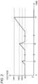
- Fig. 2 is a graph showing an exemplary voltage of the DC buses 20a and 20b of the power system of Fig. 1 .
- V0 denotes a target voltage of the DC buses 20a and 20b.
- the power supply apparatus 2 operates such that the voltage of the DC buses 20a and 20b matches or approaches the target voltage V0.
- Vth1 denotes an overvoltage threshold of the overvoltage protection circuit 23a.
- Vth2 denotes a regeneration threshold of the regeneration control circuit 3a.
- Vth3 denotes a discharge threshold of the discharge control circuit 26.
- the overvoltage protection circuit 23a stops supplying power from the power supply apparatus 2 to the motor controller 3 and the motor 4 as described above, and therefore, the voltage of the DC buses 20a and 20b becomes zero.
- the internal bus voltage of the motor controller 3 exceeds the regeneration threshold Vth2 due to the regenerative power of the motor 4
- the voltage of the DC buses 20a and 20b also exceeds the regeneration threshold Vth2 (time t2).
- the regeneration control circuit 3a consumes the regenerative power to reduce the internal bus voltage as described above, and therefore, the voltage of the DC buses 20a and 20b is reduced to the target voltage V0.
- the regeneration threshold Vth2 is set to a considerable voltage, and the regeneration control circuit 3a does not operate as long as the internal bus voltage of the motor controller 3 does not exceed the regeneration threshold Vth2, and therefore, the internal bus voltage and the DC buses 20a and 20b can not be reduced.
- the discharge threshold Vth3 is set to be smaller than the regeneration threshold Vth2, it is possible to immediately turn on the switch Q1 in response to the increase in the voltage of the DC buses 20a and 20b, to immediately reduce the voltage of the DC buses 20a and 20b.
- the power supply apparatus 2 of the embodiment it is possible to reduce the fluctuation of the voltage of the DC buses 20a and 20b, without mounting a large number of capacitors.
- the switch Q1 when the voltage of the DC buses 20a and 20b increases due to the regenerative power of the motor 4, the switch Q1 is turned on, and the power of the DC buses 20a and 20b is consumed by the resistor R1, and therefore, it is possible to reduce the fluctuation of the voltage of the DC buses 20a and 20b caused by the regenerative power of the motor 4.
- the power supply apparatus 2 of the embodiment when the voltage of the DC buses 20a and 20b increases due to the regenerative power of the motor 4, the power supply apparatus 2 continues to supply power to the motor controller 3 and the motor 4 without stopping. Therefore, then, even if the consumed power of the motor 4 rapidly increases, the power supply apparatus 2 can immediately increase its output power to supply required power to the motor 4. As described above, according to the power supply apparatus 2 of the embodiment, it is possible to reduce the fluctuation of the voltage of the DC buses 20a and 20b caused by the regenerative power and the consumed power of the motor 4 to stably maintain the voltage of the DC buses 20a and 20b, without significantly increasing the circuit size.
- the power supply apparatus 2 is provided with: a rectifier circuit 21, an inverter 22, a voltage control circuit 23, a transformer T1, a rectifier circuit 24, and a voltage feedback circuit 25, as well as the DC buses 20a and 20b, the overvoltage protection circuit 23a, the switch Q1, the resistor R1, and the discharge control circuit 26.
- the rectifier circuit 21 rectifies the AC power supplied from the AC power supply 1, into DC power.
- the inverter 22 is a power converter circuit that is provided on the primary side of the transformer T1, converts the DC power inputted from the rectifier circuit 21, into AC power at a certain voltage, and supplies the AC power to the transformer T1.
- the voltage control circuit 23 is provided on the primary side of the transformer T1, and controls the output voltage of the inverter 22 (that is, the voltage applied to a primary winding of the transformer T1). In the example of Fig. 1 , the overvoltage protection circuit 23a is integrated with the voltage control circuit 23.
- the rectifier circuit 24 rectifies AC power generated in a secondary winding of the transformer T1, and outputs the rectified AC power to the DC buses 20a and 20b.
- the voltage feedback circuit 25 is provided on the secondary side of the transformer T1, and monitors the voltage of the DC buses 20a and 20b.
- the voltage control circuit 23 and the overvoltage protection circuit 23a obtain the voltage of the DC buses 20a and 20b, from the voltage feedback circuit 25.
- the voltage control circuit 23 controls the output voltage of the inverter 22 based on the voltage of the DC buses 20a and 20b, such that the voltage of the DC buses 20a and 20b matches or approaches the target voltage V0.
- the power supply apparatus 2 is configured as an isolated power converter circuit including the transformer T1.
- Fig. 3 is a circuit diagram showing an exemplary configuration of the power supply apparatus 2 of Fig. 1 .
- Fig. 3 illustrates only a secondary circuit of the transformer T1 for ease of illustration.
- the power supply apparatus 2 is provided with the rectifier circuit 24, the voltage feedback circuit 25, the discharge control circuit 26, the switch Q1, and the resistor R1 described with reference to Fig. 1 , and further provided with an electrolytic capacitor C2 and resistors R5 and R6.
- the rectifier circuit 24 is provided with a diode D1 and an electrolytic capacitor C1.
- the diode D1 is connected to the secondary winding of the transformer T1.
- the electrolytic capacitor C1 is connected between the DC buses 20a and 20b, and smooths the voltage rectified by the diode D1.
- the voltage feedback circuit 25 is provided with: resistors R2 to R4, a variable resistor RV, a shunt regulator SRI, and a light emitting diode LED.
- the resistor R2, the shunt regulator SRI, and the light emitting diode LED are connected in series between the DC buses 20a and 20b.
- the resistors R3 and R4 are also connected in series between the DC buses 20a and 20b, and the variable resistor RV is connected in parallel to the resistor R4.
- the target voltage of the DC buses 20a and 20b is set according to the resistance of the variable resistor RV.
- the voltage of the DC buses 20a and 20b is divided by the resistors R3 and R4 and the variable resistor RV, and the divided voltage is applied to the reference terminal of the shunt regulator SR1.
- a photocoupler is constituted by the light emitting diode LED as well as a phototransistor (not illustrated) provided in a primary circuit of the transformer T1, and the light emitting diode LED notifies the voltage control circuit 23 and the overvoltage protection circuit 23a of the voltage of the DC buses 20a and 20b at a node N1.
- the resistors R5 and R6 are connected in series between the DC buses 20a and 20b, divide the voltage of the DC buses 20a and 20b at a node N2, and pass the divided voltage to the discharge control circuit 26.
- the electrolytic capacitor C2 is connected between the DC buses 20a and 20b, and smooths the voltage of the DC buses 20a and 20b.
- the discharge control circuit 26 is provided with: resistors R7 to R9, a switch Q2, a comparator CMP1, and a diode D2.
- the resistors R7 to R9 and the switch Q2 form a voltage source of a reference voltage corresponding to the discharge threshold Vth3.
- the comparator CMP1 compares the voltage of the DC buses 20a and 20b divided by the resistors R5 and R6, with the discharge threshold Vth3, and turns on the switch Q1 when the voltage of the DC buses 20a and 20b exceeds the discharge threshold Vth3.
- the discharge threshold Vth3 has hysteresis.
- the switch Q1 When the switch Q1 is turned on, the switch Q2 is also turned on at the same time, and therefore, the discharge threshold Vth3 varies.
- the discharge threshold Vth3 for turning on the switch Q1 is set to 55 V
- the discharge threshold Vth3 for turning off the switch Q1 is set to 50 V.
- the overvoltage protection circuit 23a stops supplying power from the power supply apparatus 2 to the motor controller 3 and the motor 4, before the regeneration control circuit 3a operates.
- the power supply apparatus 2 and the motor controller 3 should be configured to always satisfy Vth1 > Vth2.
- Fig. 4 is a circuit diagram showing an exemplary configuration of a power supply apparatus 2A according to a first modified embodiment of the first embodiment.
- the power supply apparatus 2A is configured in a manner similar to that of the power supply apparatus 2 of Fig. 3 , with the resistors R5 and R6 being removed.
- the discharge control circuit 26 obtains the voltage of the DC buses 20a and 20b from the voltage feedback circuit 25. Specifically, the discharge control circuit 26 obtains the voltage of the DC buses 20a and 20b at the node N2 divided by the resistors R3 and R4 and the variable resistor RV, that is, the voltage applied to the variable resistor RV, as the voltage of the DC buses 20a and 20b.
- the comparator CMP1 compares the voltage applied to the variable resistor RV, with the discharge threshold Vth3.
- the target voltage V0 of the DC buses 20a and 20b is set according to the resistance of the variable resistor RV.
- the voltage inputted from the voltage feedback circuit 25 to the comparator CMP1 is the same as that before changing the resistance of the variable resistor RV. Therefore, the discharge threshold Vth3 equivalently varies in response to the increase or decrease of the target voltage V0 of the DC buses 20a and 20b. According to the power supply apparatus 2A of Fig.
- the discharge control circuit 26 is operable to turn on the switch Q1 when the voltage of the DC buses 20a and 20b reaches a predetermined multiple of the target voltage V0, for example, 1.3 times, regardless of the magnitude of the target voltage V0 of the DC buses 20a and 20b. For example, in the case where the target voltage V0 is 50 V, the discharge control circuit 26 turns on the switch Q1 when the voltage of the DC buses 20a and 20b reaches 65 V. In addition, in the case where the target voltage V0 is 55 V, the discharge control circuit 26 turns on the switch Q1 when the voltage of the DC buses 20a and 20b reaches 71.5 V.
- Fig. 5 is a circuit diagram showing an exemplary configuration of a power supply apparatus 2B according to a second modified embodiment of the first embodiment.
- the power supply apparatus 2B is provided with a diode D3, as well as the components of the power supply apparatus 2A of Fig. 4 .
- the overvoltage protection circuit 23a obtains the voltage of the DC buses 20a and 20b at the node N1, from the voltage feedback circuit 25.
- the discharge control circuit 26 obtains the voltage of the DC buses 20a and 20b at the node N2 divided by the resistors R3 and R4 and the variable resistor RV, from the voltage feedback circuit 25.
- the node N2 is provided closer to the motor controller 3 than the node N1.
- the diode D3 is inserted into the DC bus 20a so as to block the current flowing from the node N2 to the node N1.
- the power supply apparatus 2 and the motor controller 3 should be configured to always satisfy Vth1 > Vth2, in order to operate the regeneration control circuit 3a without stopping supplying power from the power supply apparatus 2 to the motor controller 3 and the motor 4, as described above.
- the power supply apparatus 2B of Fig. 4 since the diode D3 is inserted between the nodes N1 and N2, even if the voltage of the node N2 increases due to the regenerative power, the voltage of the node N1 does not increase.
- the voltage control circuit 23 obtains the voltage of the DC buses 20a and 20b at the node N2, from the voltage feedback circuit 25. As described above, the voltage of the DC buses 20a and 20b at the node N2 divided by the resistors R3 and R4 and the variable resistor RV is applied to the reference terminal of the shunt regulator SRI, and this voltage is notified to the voltage control circuit 23 via the photocoupler including the light emitting diode LED.
- the power supply apparatuses 2, 2A, and 2B of the first embodiment it is possible to reduce the fluctuation of the voltage of the DC buses 20a and 20b caused by the regenerative power and the consumed power of the motor 4 to stably maintain the voltage of the DC buses 20a and 20b, without significantly increasing the circuit size.
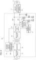
- Fig. 6 is a block diagram showing an exemplary configuration of a power system according to a second embodiment.
- the power system of Fig. 6 is provided with a power supply apparatus 2C, instead of the power supply apparatus 2 for the power system of Fig. 1 .
- the power supply apparatus 2C is provided with an anomaly determination circuit 27 and a switch Q3, as well as the components of the power supply apparatus 2 of Fig. 1 .
- the anomaly determination circuit 27 determines anomaly of a primary circuit of the transformer T1, that is, the inverter 22 or the voltage control circuit 23.
- the anomaly of the inverter 22 or the voltage control circuit 23 includes, for example, an excessively high output voltage being generated from the inverter 22 due to a failure of the inverter 22 or the voltage control circuit 23, or due to a failure in voltage feedback.
- the gate of the switch Q1 is grounded via the switch Q3.
- the anomaly determination circuit 27 turns on the switch Q3 to control the switch Q1 to stop consuming power of DC buses 20a and 20b.
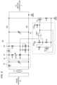
- Fig. 7 is a circuit diagram showing an exemplary configuration of the power supply apparatus 2C of Fig. 6 .
- Fig. 7 illustrates only a secondary circuit of the transformer T1 for ease of illustration.
- the anomaly determination circuit 27 is provided with the reference voltage source E1 and the comparator CMP2.
- the comparator CMP2 compares the voltage at a node on the secondary circuit of the transformer T1, with the voltage of the reference voltage source E1, and determines that an anomaly has occurred in the inverter 22 or the voltage control circuit 23, when the voltage of the voltage feedback circuit 25 exceeds the voltage of the reference voltage source E1.
- the comparator CMP2 monitors the voltage at the node N1.
- the voltage of the node N1 in the secondary circuit of the transformer T1 increases. Since the diode D3 is inserted into the DC bus 20a so as to block the current flowing from the node N2 to the node N1 as described above, the voltage at the node N1 does not increase due to the regenerative power of the motor 4.
- the other components of the power supply apparatus 2C are configured in a manner similar to that of the corresponding components of the power supply apparatus 2B of Fig. 5 .
- Fig. 8 is a circuit diagram showing an exemplary configuration of a power supply apparatus 2D according to a modified embodiment of the second embodiment.
- the power supply apparatus 2D is provided with a voltage feedback circuit 25D and a discharge control circuit 26D, instead of the voltage feedback circuit 25 and the discharge control circuit 26 of Fig. 7 , and further provided with resistors R15 and R16.
- the voltage feedback circuit 25D is configured in a manner similar to that of the voltage feedback circuit 25 of Fig. 7 , with the variable resistor RV being removed.
- the discharge control circuit 26D is provided with: resistors R11 to R14, a shunt regulator SR2, a switch Q11, and a diode D11.
- the switch Q11 is, for example, a bipolar transistor.
- the emitter of the switch Q11 is connected to the DC bus 20a, and the collector of the switch Q11 is grounded via the resistors R15 and R16 connected in series with each other.
- the connection point between the resistors R15 and R16 is connected to the gate of the switch Q1.
- the base of the switch Q11 is connected to the cathode of the shunt regulator SR2 via the resistor R13.
- the resistors R11 and R12 divide the voltage of the DC buses 20a and 20b at the node N2, apply the divided voltage to the control terminal of the shunt regulator SR2, and apply the divided voltage to the cathode of the diode D11 via the resistor R14.
- the anode of diode D11 is connected to the collector of switch Q11.
- the cathode of the shunt regulator SR2 becomes a low level, and the switch Q11 is turned on.
- the gate voltage of the switch Q1 becomes a high level, and the switch Q1 is turned on.
- the discharge threshold Vth3 for turning on the switch Q1 has hysteresis due to the diode D11 and the resistor R14.
- the diode D3 is inserted into the DC bus 20a so as to block the current flowing from the node N2 to the node N1.
- the power supply apparatus 2D of Fig. 8 is provided with the anomaly determination circuit 27, it is possible to prevent the switch Q1 and the resistor R1 from generating excessively high heat, even if an anomaly occurs in the inverter 22 or the voltage control circuit 23, in a manner similar to that of the power supply apparatus 2C of Fig. 7 .
- the power supply apparatuses 2C and 2D of the second embodiment it is possible to reduce the fluctuation of the voltage of the DC buses 20a and 20b caused by the regenerative power and the consumed power of the motor 4 to stably maintain the voltage of the DC buses 20a and 20b, without significantly increasing the circuit size, in a manner similar to that of the power supply apparatuses 2, 2A, and 2B of the first embodiment.
- the power supply apparatuses 2C and 2D of the second embodiment even if an anomaly occurs in the inverter 22 or the voltage control circuit 23, it is possible to prevent the switch Q1 and the resistor R1 from generating excessively high heat.
- Fig. 3 and others illustrate exemplary cases where the rectifier circuit 24 is configured as a half-wave rectifier circuit including one diode D1
- the rectifier circuit may be configured as a full-wave rectifier circuit.
- the power supply apparatus may be configured to be supplied with power from a DC power supply, instead of the AC power supply.
- the power supply apparatus may be configured as a non-isolated power converter circuit not including a transformer.
- FIGs. 1 and 6 illustrate exemplary cases where the regeneration control circuit 3a is integrated with the motor controller 3, the regeneration control circuit 3a may be provided separately from the motor controller 3.
- the power supply apparatus may be configured to supply power to any load apparatus that generates regenerative power, without being limited to the motor controller 3 and the motor 4.
- the power supply apparatuses according to aspects of the present disclosure may be expressed as follows.
- the power supply apparatus 2, 2A to 2D for supplying DC power to a load apparatus is provided with: a direct current (DC) buses 20a and 20b, an overvoltage protection circuit 23a, a discharge circuit, and a discharge control circuit 26.
- the direct current (DC) bus (20a, 20b) are connected to the load apparatus.
- the overvoltage protection circuit 23a is configured to stop supplying power from the power supply apparatus 2 to the load apparatus, when a voltage of the DC bus (20a, 20b) exceeds a predetermined overvoltage threshold.
- the discharge circuit is connected to the DC bus (20a, 20b).
- the discharge control circuit 26 is configured to control the discharge circuit to consume power of the DC bus (20a, 20b) to reduce the voltage of the DC bus (20a, 20b), when the voltage of the DC bus (20a, 20b) exceeds a discharge threshold, the discharge threshold being higher than a target voltage of the DC bus (20a, 20b) and lower than the overvoltage threshold.
- the overvoltage protection circuit 23a is configured to monitor the voltage of the DC bus (20a, 20b) at a first node N1.
- the discharge control circuit 26 is configured to monitor the voltage of the DC bus (20a, 20b) at a second node N2 closer to the load apparatus than the first node N1.
- the power supply apparatus 2 is further provided with a diode D3 configured to block a current flowing from the second node N2 to the first node N1.
- the power supply apparatus 2A to 2C is further provided with: a transformer T1, a inverter 22, a voltage control circuit 23, and a voltage feedback circuit 25.
- the inverter 22 is provided on a primary side of the transformer T1, and configured to convert an input voltage into an output voltage and supply the output voltage to the transformer T1.
- the voltage control circuit 23 is provided on the primary side of the transformer T1, and configured to control an output voltage of the inverter 22.
- the voltage feedback circuit 25 is provided on a secondary side of the transformer T1, and configured to monitor the voltage of the DC bus (20a, 20b).
- the overvoltage protection circuit 23a, the voltage control circuit 23, and the discharge control circuit 26 obtain the voltage of the DC bus (20a, 20b) from the voltage feedback circuit 25.
- the voltage feedback circuit 25 is provided with a variable resistor RV configured to set the target voltage of the DC bus (20a, 20b).
- the discharge control circuit 26 is configured to obtain a voltage applied to the variable resistor RV, as the voltage of the DC bus (20a, 20b).
- the power supply apparatus 2C, 2D is further provided with an anomaly determination circuit 27 configured to determine an anomaly of the inverter 22 or the voltage control circuit 23.
- the anomaly determination circuit 27 is configured to control the discharge circuit to stop consuming the power of the DC bus (20a, 20b), when an anomaly occurs in the inverter 22 or the voltage control circuit 23.
- the discharge threshold has hysteresis.
- the load apparatus includes a motor 4.
- the power supply apparatus is available to supply power to a load apparatus that generates regenerative power.
Landscapes
- Engineering & Computer Science (AREA)
- Power Engineering (AREA)
- Inverter Devices (AREA)
- Direct Current Feeding And Distribution (AREA)
- Dc-Dc Converters (AREA)
- Emergency Protection Circuit Devices (AREA)
- Stopping Of Electric Motors (AREA)
Abstract
Description
- The present disclosure relates to a power supply apparatus.
- When a load apparatus includes a motor, the motor's regenerative power may flow to preceding circuits (motor controller, power supply apparatus, and the like). For example,
Patent Document 1 discloses a direct current (DC) stabilized power supply system capable of absorbing power fluctuation to maintain power supply quality when a motor generates regenerative power. - PATENT DOCUMENT 1: Japanese Patent No.
JP 6502758 B - When a motor generates regenerative power, the voltage of its preceding circuits, such as a DC bus of the power supply apparatus, may increase. Typically, when the DC bus voltage has increased, the power supply apparatus determines that it is not necessary to further supply power, and stops operation of the circuit (for example, switching operation of the inverter). When the consumed power of the load apparatus rapidly increases during a period in which the circuit is not in operation, it may take a long response time to supply required power to the load apparatus, and the DC bus voltage may decrease. Therefore, even when the regenerative power and the consumed power of the load apparatus fluctuate rapidly, it is required to reduce the fluctuation of the DC bus voltage to stably maintain the DC bus voltage.
- In addition, in order to reduce the fluctuation of the DC bus voltage caused by the regenerative power and the consumed power of the load apparatus, for example, it may be possible to connect a large number of capacitors to the DC bus. However, in this case, the size of the power supply apparatus increases in order to mount the large number of capacitors. In addition, since the capacitors simply receive the regenerative power, the DC bus voltage itself increases, and it is not possible to sufficiently reduce the fluctuation of the DC bus voltage.
- An object of the present disclosure is to provide a power supply apparatus capable of reducing fluctuation of a DC bus voltage caused by regenerative power and consumed power of a load apparatus to stably maintain the DC bus voltage, without significantly increasing the circuit size.
- According to a power supply apparatus of an aspect of the present disclosure, the power supply apparatus for supplying DC power to a load apparatus is provided with: a direct current (DC) bus, an overvoltage protection circuit, a discharge circuit, and a discharge control circuit. The direct current (DC) bus is connected to the load apparatus. The overvoltage protection circuit is configured to stop supplying power from the power supply apparatus to the load apparatus, when a voltage of the DC bus exceeds a predetermined overvoltage threshold. The discharge circuit is connected to the DC bus. The discharge control circuit is configured to control the discharge circuit to consume power of the DC bus to reduce the voltage of the DC bus, when the voltage of the DC bus exceeds a discharge threshold, the discharge threshold being higher than a target voltage of the DC bus and lower than the overvoltage threshold.
- With such a configuration, it is possible to reduce the fluctuation of the DC bus voltage caused by the regenerative power and the consumed power of the load apparatus to stably maintain the DC bus voltage, without significantly increasing the circuit size.
- According to a power supply apparatus of an aspect of the present disclosure, the overvoltage protection circuit is configured to monitor the voltage of the DC bus at a first node. The discharge control circuit is configured to monitor the voltage of the DC bus at a second node closer to the load apparatus than the first node. The power supply apparatus is further provided with a diode configured to block a current flowing from the second node to the first node.
- With such a configuration, even if the overvoltage threshold is lower than a regeneration threshold, it is possible to consume the regenerative power using the discharge circuit, without stopping supplying power from the power supply apparatus to the load apparatus, and consume the regenerative power by the load apparatus itself.
- According to a power supply apparatus of an aspect of the present disclosure, the power supply apparatus is further provided with: a transformer, a power converter circuit, a voltage control circuit, and a voltage feedback circuit. The power converter circuit is provided on a primary side of the transformer, and configured to convert an input voltage into an output voltage and supply the output voltage to the transformer. The voltage control circuit is provided on the primary side of the transformer, and configured to control an output voltage of the power converter circuit. The voltage feedback circuit is provided on a secondary side of the transformer, and configured to monitor the voltage of the DC bus. The overvoltage protection circuit, the voltage control circuit, and the discharge control circuit obtain the voltage of the DC bus from the voltage feedback circuit.
- With such a configuration, the overvoltage protection circuit, the voltage control circuit, and the discharge control circuit can monitor the voltage of the DC bus.
- According to a power supply apparatus of an aspect of the present disclosure, the voltage feedback circuit is provided with a variable resistor configured to set the target voltage of the DC bus. The discharge control circuit is configured to obtain a voltage applied to the variable resistor, as the voltage of the DC bus.
- With such a configuration, the discharge threshold can be changed in response to the increase or decrease of the target voltage of the DC bus.
- According to a power supply apparatus of an aspect of the present disclosure, the power supply apparatus is further provided with an anomaly determination circuit configured to determine an anomaly of the power converter circuit or the voltage control circuit. The anomaly determination circuit is configured to control the discharge circuit to stop consuming the power of the DC bus, when an anomaly occurs in the power converter circuit or the voltage control circuit.
- With such a configuration, even if an anomaly occurs in the power converter circuit or the voltage control circuit, it is possible to prevent the discharge circuit from generating excessively high heat.
- According to a power supply apparatus of an aspect of the present disclosure, the discharge threshold has hysteresis.
- With such a configuration, it is possible to reduce the number of transitions between on and off of the discharge circuit to stably operate the power supply apparatus.
- According to a power supply apparatus of an aspect of the present disclosure, the load apparatus includes a motor.
- With such a configuration, the power supply apparatus can supply power to the load apparatus that generate the regenerative power.
- According to the power supply apparatus of one aspect of the present disclosure, it is possible to reduce the fluctuation of the DC bus voltage caused by the regenerative power and the consumed power of the load apparatus to stably maintain the DC bus voltage, without significantly increasing the circuit size.
-
-
Fig. 1 is a block diagram showing an exemplary configuration of a power system according to a first embodiment. -
Fig. 2 is a graph showing an exemplary voltage ofDC buses Fig. 1 . -
Fig. 3 is a circuit diagram showing an exemplary configuration of apower supply apparatus 2 ofFig. 1 . -
Fig. 4 is a circuit diagram showing an exemplary configuration of apower supply apparatus 2A according to a first modified embodiment of the first embodiment. -
Fig. 5 is a circuit diagram showing an exemplary configuration of apower supply apparatus 2B according to a second modified embodiment of the first embodiment. -
Fig. 6 is a block diagram showing an exemplary configuration of a power system according to a second embodiment. -
Fig. 7 is a circuit diagram showing an exemplary configuration of apower supply apparatus 2C ofFig. 6 . -
Fig. 8 is a circuit diagram showing an exemplary configuration of apower supply apparatus 2D according to a modified embodiment of the second embodiment. - Hereinafter, an embodiment according to one aspect of the present disclosure will be described with reference to the drawings. In the drawings, the same reference signs denote similar components.
-
Fig. 1 is a block diagram showing an exemplary configuration of a power system according to a first embodiment. The power system ofFig. 1 is provided with: anAC power supply 1, apower supply apparatus 2, amotor controller 3, and a motor 4. - The
AC power supply 1 may be, for example, a commercial single-phase or three-phase AC power supply. - The
power supply apparatus 2 is supplied with power from theAC power supply 1, and then supplies DC power to themotor controller 3 and the motor 4, which are load apparatuses. Thepower supply apparatus 2 is provided with, at least,DC buses overvoltage protection circuit 23a, a switch Q1, a resistor R1, and adischarge control circuit 26. TheDC buses motor controller 3 and the motor 4. Theovervoltage protection circuit 23a stops supplying power from thepower supply apparatus 2 to themotor controller 3 and the motor 4, when the voltage of theDC buses DC buses positive DC bus 20a and thenegative DC bus 20b. The switch Q1 and the resistor R1 form a discharge circuit connected to theDC buses DC buses DC buses discharge control circuit 26 turns on the switch Q1, and therefore, the power of theDC buses DC buses - The
motor controller 3 is supplied with power from thepower supply apparatus 2, and controls operation of the motor 4. The motor 4 may generate regenerative power, and the generated regenerative power flows to theDC buses power supply apparatus 2 via themotor controller 3. Themotor controller 3 is provided with aregeneration control circuit 3a that consumes regenerative power to reduce the voltage of its internal bus (not shown), when the internal bus voltage exceeds a predetermined regeneration threshold due to the regenerative power. -
Fig. 2 is a graph showing an exemplary voltage of theDC buses Fig. 1 . V0 denotes a target voltage of theDC buses power supply apparatus 2 operates such that the voltage of theDC buses overvoltage protection circuit 23a. Vth2 denotes a regeneration threshold of theregeneration control circuit 3a. Vth3 denotes a discharge threshold of thedischarge control circuit 26. - When the voltage of the
DC buses overvoltage protection circuit 23a stops supplying power from thepower supply apparatus 2 to themotor controller 3 and the motor 4 as described above, and therefore, the voltage of theDC buses motor controller 3 exceeds the regeneration threshold Vth2 due to the regenerative power of the motor 4, the voltage of theDC buses regeneration control circuit 3a consumes the regenerative power to reduce the internal bus voltage as described above, and therefore, the voltage of theDC buses regeneration control circuit 3a does not operate as long as the internal bus voltage of themotor controller 3 does not exceed the regeneration threshold Vth2, and therefore, the internal bus voltage and theDC buses power supply apparatus 2 ofFig. 1 , since the discharge threshold Vth3 is set to be smaller than the regeneration threshold Vth2, it is possible to immediately turn on the switch Q1 in response to the increase in the voltage of theDC buses DC buses - According to the
power supply apparatus 2 of the embodiment, it is possible to reduce the fluctuation of the voltage of theDC buses power supply apparatus 2 of the embodiment, when the voltage of theDC buses DC buses DC buses power supply apparatus 2 of the embodiment, when the voltage of theDC buses power supply apparatus 2 continues to supply power to themotor controller 3 and the motor 4 without stopping. Therefore, then, even if the consumed power of the motor 4 rapidly increases, thepower supply apparatus 2 can immediately increase its output power to supply required power to the motor 4. As described above, according to thepower supply apparatus 2 of the embodiment, it is possible to reduce the fluctuation of the voltage of theDC buses DC buses - Hereinafter, the power supply apparatus according to the first embodiment will be further described.
- Referring to
Fig. 1 , thepower supply apparatus 2 is provided with: arectifier circuit 21, aninverter 22, avoltage control circuit 23, a transformer T1, arectifier circuit 24, and avoltage feedback circuit 25, as well as theDC buses overvoltage protection circuit 23a, the switch Q1, the resistor R1, and thedischarge control circuit 26. - The
rectifier circuit 21 rectifies the AC power supplied from theAC power supply 1, into DC power. Theinverter 22 is a power converter circuit that is provided on the primary side of the transformer T1, converts the DC power inputted from therectifier circuit 21, into AC power at a certain voltage, and supplies the AC power to the transformer T1. Thevoltage control circuit 23 is provided on the primary side of the transformer T1, and controls the output voltage of the inverter 22 (that is, the voltage applied to a primary winding of the transformer T1). In the example ofFig. 1 , theovervoltage protection circuit 23a is integrated with thevoltage control circuit 23. Therectifier circuit 24 rectifies AC power generated in a secondary winding of the transformer T1, and outputs the rectified AC power to theDC buses voltage feedback circuit 25 is provided on the secondary side of the transformer T1, and monitors the voltage of theDC buses voltage control circuit 23 and theovervoltage protection circuit 23a obtain the voltage of theDC buses voltage feedback circuit 25. Thevoltage control circuit 23 controls the output voltage of theinverter 22 based on the voltage of theDC buses DC buses - In the example of
Fig. 1 , thepower supply apparatus 2 is configured as an isolated power converter circuit including the transformer T1. -
Fig. 3 is a circuit diagram showing an exemplary configuration of thepower supply apparatus 2 ofFig. 1 .Fig. 3 illustrates only a secondary circuit of the transformer T1 for ease of illustration. Thepower supply apparatus 2 is provided with therectifier circuit 24, thevoltage feedback circuit 25, thedischarge control circuit 26, the switch Q1, and the resistor R1 described with reference toFig. 1 , and further provided with an electrolytic capacitor C2 and resistors R5 and R6. - The
rectifier circuit 24 is provided with a diode D1 and an electrolytic capacitor C1. The diode D1 is connected to the secondary winding of the transformer T1. The electrolytic capacitor C1 is connected between theDC buses - The
voltage feedback circuit 25 is provided with: resistors R2 to R4, a variable resistor RV, a shunt regulator SRI, and a light emitting diode LED. The resistor R2, the shunt regulator SRI, and the light emitting diode LED are connected in series between theDC buses DC buses DC buses DC buses voltage control circuit 23 and theovervoltage protection circuit 23a of the voltage of theDC buses - The resistors R5 and R6 are connected in series between the
DC buses DC buses discharge control circuit 26. - The electrolytic capacitor C2 is connected between the
DC buses DC buses - The
discharge control circuit 26 is provided with: resistors R7 to R9, a switch Q2, a comparator CMP1, and a diode D2. The resistors R7 to R9 and the switch Q2 form a voltage source of a reference voltage corresponding to the discharge threshold Vth3. The comparator CMP1 compares the voltage of theDC buses DC buses Fig. 3 , the discharge threshold Vth3 has hysteresis. When the switch Q1 is turned on, the switch Q2 is also turned on at the same time, and therefore, the discharge threshold Vth3 varies. For example, when the target voltage V0 of theDC buses - In the example of
Fig. 3 , when the switch Q1 is turned on, a constant current flows through the switch Q1 and the resistor R1. - In the case where the regeneration threshold Vth2 is higher than the overvoltage threshold Vth1, when the voltage of the
DC buses overvoltage protection circuit 23a stops supplying power from thepower supply apparatus 2 to themotor controller 3 and the motor 4, before theregeneration control circuit 3a operates. In order to operate theregeneration control circuit 3a without stopping supplying power from thepower supply apparatus 2 to themotor controller 3 and the motor 4, thepower supply apparatus 2 and themotor controller 3 should be configured to always satisfy Vth1 > Vth2. -
Fig. 4 is a circuit diagram showing an exemplary configuration of apower supply apparatus 2A according to a first modified embodiment of the first embodiment. Thepower supply apparatus 2A is configured in a manner similar to that of thepower supply apparatus 2 ofFig. 3 , with the resistors R5 and R6 being removed. Further, referring toFig. 4 , thedischarge control circuit 26 obtains the voltage of theDC buses voltage feedback circuit 25. Specifically, thedischarge control circuit 26 obtains the voltage of theDC buses DC buses DC buses power supply apparatus 2A ofFig. 4 , even if the voltage of theDC buses voltage feedback circuit 25 to the comparator CMP1 is the same as that before changing the resistance of the variable resistor RV. Therefore, the discharge threshold Vth3 equivalently varies in response to the increase or decrease of the target voltage V0 of theDC buses power supply apparatus 2A ofFig. 4 , thedischarge control circuit 26 is operable to turn on the switch Q1 when the voltage of theDC buses DC buses discharge control circuit 26 turns on the switch Q1 when the voltage of theDC buses discharge control circuit 26 turns on the switch Q1 when the voltage of theDC buses -
Fig. 5 is a circuit diagram showing an exemplary configuration of apower supply apparatus 2B according to a second modified embodiment of the first embodiment. Thepower supply apparatus 2B is provided with a diode D3, as well as the components of thepower supply apparatus 2A ofFig. 4 . As described above, theovervoltage protection circuit 23a obtains the voltage of theDC buses voltage feedback circuit 25. In addition, thedischarge control circuit 26 obtains the voltage of theDC buses voltage feedback circuit 25. The node N2 is provided closer to themotor controller 3 than the node N1. The diode D3 is inserted into theDC bus 20a so as to block the current flowing from the node N2 to the node N1. In the configurations of thepower supply apparatus 2 ofFig. 3 and thepower supply apparatus 2A ofFig. 4 , thepower supply apparatus 2 and themotor controller 3 should be configured to always satisfy Vth1 > Vth2, in order to operate theregeneration control circuit 3a without stopping supplying power from thepower supply apparatus 2 to themotor controller 3 and the motor 4, as described above. On the other hand, according to thepower supply apparatus 2B ofFig. 4 , since the diode D3 is inserted between the nodes N1 and N2, even if the voltage of the node N2 increases due to the regenerative power, the voltage of the node N1 does not increase. Therefore, it is possible to prevent theovervoltage protection circuit 23a from erroneously stopping supplying power from thepower supply apparatus 2B to themotor controller 3 and the motor 4. Therefore, according to thepower supply apparatus 2B ofFig. 4 , even if Vth1 < Vth2, it is possible to consume the regenerative power using thedischarge control circuit 26, the switch Q1, and the resistor R1, without stopping supplying power from thepower supply apparatus 2 to themotor controller 3 and the motor 4, and operate theregeneration control circuit 3a. - Note that in the example of
Fig. 5 , thevoltage control circuit 23 obtains the voltage of theDC buses voltage feedback circuit 25. As described above, the voltage of theDC buses voltage control circuit 23 via the photocoupler including the light emitting diode LED. - According to the
power supply apparatuses DC buses DC buses - Hereinafter, a power supply apparatus according to a second embodiment will be described.
-
Fig. 6 is a block diagram showing an exemplary configuration of a power system according to a second embodiment. The power system ofFig. 6 is provided with apower supply apparatus 2C, instead of thepower supply apparatus 2 for the power system ofFig. 1 . Thepower supply apparatus 2C is provided with ananomaly determination circuit 27 and a switch Q3, as well as the components of thepower supply apparatus 2 ofFig. 1 . - The
anomaly determination circuit 27 determines anomaly of a primary circuit of the transformer T1, that is, theinverter 22 or thevoltage control circuit 23. The anomaly of theinverter 22 or thevoltage control circuit 23 includes, for example, an excessively high output voltage being generated from theinverter 22 due to a failure of theinverter 22 or thevoltage control circuit 23, or due to a failure in voltage feedback. The gate of the switch Q1 is grounded via the switch Q3. When an anomaly occurs in theinverter 22 or thevoltage control circuit 23, theanomaly determination circuit 27 turns on the switch Q3 to control the switch Q1 to stop consuming power ofDC buses -
Fig. 7 is a circuit diagram showing an exemplary configuration of thepower supply apparatus 2C ofFig. 6 .Fig. 7 illustrates only a secondary circuit of the transformer T1 for ease of illustration. Theanomaly determination circuit 27 is provided with the reference voltage source E1 and the comparator CMP2. The comparator CMP2 compares the voltage at a node on the secondary circuit of the transformer T1, with the voltage of the reference voltage source E1, and determines that an anomaly has occurred in theinverter 22 or thevoltage control circuit 23, when the voltage of thevoltage feedback circuit 25 exceeds the voltage of the reference voltage source E1. In the example ofFig. 7 , the comparator CMP2 monitors the voltage at the node N1. When an anomaly occurs in theinverter 22 or thevoltage control circuit 23, and an excessively high voltage is generated in a primary circuit of the transformer T1, the voltage of the node N1 in the secondary circuit of the transformer T1 increases. Since the diode D3 is inserted into theDC bus 20a so as to block the current flowing from the node N2 to the node N1 as described above, the voltage at the node N1 does not increase due to the regenerative power of the motor 4. The other components of thepower supply apparatus 2C are configured in a manner similar to that of the corresponding components of thepower supply apparatus 2B ofFig. 5 . In the case where the voltage of theDC buses discharge control circuit 26 turns on the switch Q1, the switch Q1 and the resistor R1 may be damaged by generating excessively high heat. On the other hand, when thepower supply apparatus 2C ofFig. 7 determines that an anomaly has occurred in theinverter 22 or thevoltage control circuit 23, thepower supply apparatus 2C forcibly turns off the switch Q1 by turning on the switch Q3. As a result, even if an anomaly occurs in theinverter 22 or thevoltage control circuit 23, it is possible to prevent the switch Q1 and the resistor R1 from generating excessively high heat. -
Fig. 8 is a circuit diagram showing an exemplary configuration of apower supply apparatus 2D according to a modified embodiment of the second embodiment. Thepower supply apparatus 2D is provided with avoltage feedback circuit 25D and adischarge control circuit 26D, instead of thevoltage feedback circuit 25 and thedischarge control circuit 26 ofFig. 7 , and further provided with resistors R15 and R16. - The
voltage feedback circuit 25D is configured in a manner similar to that of thevoltage feedback circuit 25 ofFig. 7 , with the variable resistor RV being removed. - The
discharge control circuit 26D is provided with: resistors R11 to R14, a shunt regulator SR2, a switch Q11, and a diode D11. The switch Q11 is, for example, a bipolar transistor. The emitter of the switch Q11 is connected to theDC bus 20a, and the collector of the switch Q11 is grounded via the resistors R15 and R16 connected in series with each other. The connection point between the resistors R15 and R16 is connected to the gate of the switch Q1. The base of the switch Q11 is connected to the cathode of the shunt regulator SR2 via the resistor R13. The resistors R11 and R12 divide the voltage of theDC buses DC buses - The diode D3 is inserted into the
DC bus 20a so as to block the current flowing from the node N2 to the node N1. - Since the
power supply apparatus 2D ofFig. 8 is provided with theanomaly determination circuit 27, it is possible to prevent the switch Q1 and the resistor R1 from generating excessively high heat, even if an anomaly occurs in theinverter 22 or thevoltage control circuit 23, in a manner similar to that of thepower supply apparatus 2C ofFig. 7 . - According to the
power supply apparatuses DC buses DC buses power supply apparatuses power supply apparatuses inverter 22 or thevoltage control circuit 23, it is possible to prevent the switch Q1 and the resistor R1 from generating excessively high heat. - Although the embodiments of the present disclosure have been described in detail above, the above descriptions are mere examples of the present disclosure in all respects. Needless to say, various improvements and modifications can be made without departing from the scope of the present disclosure. For example, the following changes can be made. Hereinafter, components similar to those of the above embodiments are indicated by similar reference signs, and points similar to those of the above embodiments will be omitted as appropriate. The following modified embodiments can be combined as appropriate.
- Although
Fig. 3 and others illustrate exemplary cases where therectifier circuit 24 is configured as a half-wave rectifier circuit including one diode D1, the rectifier circuit may be configured as a full-wave rectifier circuit. - In addition, the power supply apparatus may be configured to be supplied with power from a DC power supply, instead of the AC power supply.
- In addition, the power supply apparatus may be configured as a non-isolated power converter circuit not including a transformer.
- Although
Figs. 1 and6 illustrate exemplary cases where theregeneration control circuit 3a is integrated with themotor controller 3, theregeneration control circuit 3a may be provided separately from themotor controller 3. - The power supply apparatus may be configured to supply power to any load apparatus that generates regenerative power, without being limited to the
motor controller 3 and the motor 4. - The power supply apparatuses according to aspects of the present disclosure may be expressed as follows.
- According to a power supply apparatus of an aspect of the present disclosure, the
power supply apparatus buses overvoltage protection circuit 23a, a discharge circuit, and adischarge control circuit 26. The direct current (DC) bus (20a, 20b) are connected to the load apparatus. Theovervoltage protection circuit 23a is configured to stop supplying power from thepower supply apparatus 2 to the load apparatus, when a voltage of the DC bus (20a, 20b) exceeds a predetermined overvoltage threshold. The discharge circuit is connected to the DC bus (20a, 20b). Thedischarge control circuit 26 is configured to control the discharge circuit to consume power of the DC bus (20a, 20b) to reduce the voltage of the DC bus (20a, 20b), when the voltage of the DC bus (20a, 20b) exceeds a discharge threshold, the discharge threshold being higher than a target voltage of the DC bus (20a, 20b) and lower than the overvoltage threshold. - According to a
power supply apparatus 2B to 2D of an aspect of the present disclosure, theovervoltage protection circuit 23a is configured to monitor the voltage of the DC bus (20a, 20b) at a first node N1. Thedischarge control circuit 26 is configured to monitor the voltage of the DC bus (20a, 20b) at a second node N2 closer to the load apparatus than the first node N1. Thepower supply apparatus 2 is further provided with a diode D3 configured to block a current flowing from the second node N2 to the first node N1. - According to a
power supply apparatus 2A to 2C of an aspect of the present disclosure, thepower supply apparatus 2A to 2C is further provided with: a transformer T1, ainverter 22, avoltage control circuit 23, and avoltage feedback circuit 25. Theinverter 22 is provided on a primary side of the transformer T1, and configured to convert an input voltage into an output voltage and supply the output voltage to the transformer T1. Thevoltage control circuit 23 is provided on the primary side of the transformer T1, and configured to control an output voltage of theinverter 22. Thevoltage feedback circuit 25 is provided on a secondary side of the transformer T1, and configured to monitor the voltage of the DC bus (20a, 20b). Theovervoltage protection circuit 23a, thevoltage control circuit 23, and thedischarge control circuit 26 obtain the voltage of the DC bus (20a, 20b) from thevoltage feedback circuit 25. - According to a
power supply apparatus voltage feedback circuit 25 is provided with a variable resistor RV configured to set the target voltage of the DC bus (20a, 20b). Thedischarge control circuit 26 is configured to obtain a voltage applied to the variable resistor RV, as the voltage of the DC bus (20a, 20b). - According to a
power supply apparatus power supply apparatus anomaly determination circuit 27 configured to determine an anomaly of theinverter 22 or thevoltage control circuit 23. Theanomaly determination circuit 27 is configured to control the discharge circuit to stop consuming the power of the DC bus (20a, 20b), when an anomaly occurs in theinverter 22 or thevoltage control circuit 23. - According to a
power supply apparatus - According to a
power supply apparatus - The power supply apparatus according to each aspect of the present disclosure is available to supply power to a load apparatus that generates regenerative power.
-
- 1: AC power supply
- 2, 2A to 2D: power supply apparatus
- 3: motor controller
- 3a: regeneration control circuit
- 4: motor
- 20a, 20b: direct current (DC) bus
- 21: rectifier circuit
- 22: inverter
- 23, voltage control circuit
- 23a: overvoltage protection circuit
- 24: rectifier circuit
- 25, 25D: voltage feedback circuit
- 26: discharge control circuit
- 27: anomaly determination circuit
- C1, C2: electrolytic capacitor
- CMP1, CMP2: comparator
- D1 to D3, D11: diode
- E1: reference voltage source
- LED: light emitting diode
- Q1 to Q3: switch
- R1 to R9, R11 to R16: resistor
- SR1, SR2: shunt regulator
- T1: transformer
- RV: variable resistor
Claims (7)
- A power supply apparatus for supplying DC power to a load apparatus, the power supply apparatus comprising:a direct current (DC) bus connected to the load apparatus;an overvoltage protection circuit configured to stop supplying power from the power supply apparatus to the load apparatus, when a voltage of the DC bus exceeds a predetermined overvoltage threshold;a discharge circuit connected to the DC bus; anda discharge control circuit configured to control the discharge circuit to consume power of the DC bus to reduce the voltage of the DC bus, when the voltage of the DC bus exceeds a discharge threshold, the discharge threshold being higher than a target voltage of the DC bus and lower than the overvoltage threshold.
- The power supply apparatus as claimed in claim 1,wherein the overvoltage protection circuit is configured to monitor the voltage of the DC bus at a first node,wherein the discharge control circuit is configured to monitor the voltage of the DC bus at a second node closer to the load apparatus than the first node, andwherein the power supply apparatus further comprises a diode configured to block a current flowing from the second node to the first node.
- The power supply apparatus as claimed in claim 1 or 2, further comprising:a transformer;a power converter circuit provided on a primary side of the transformer, and configured to convert an input voltage into an output voltage and supply the output voltage to the transformer;a voltage control circuit provided on the primary side of the transformer, and configured to control an output voltage of the power converter circuit; anda voltage feedback circuit provided on a secondary side of the transformer, and configured to monitor the voltage of the DC bus,wherein the overvoltage protection circuit, the voltage control circuit, and the discharge control circuit obtain the voltage of the DC bus from the voltage feedback circuit.
- The power supply apparatus as claimed in claim 3,wherein the voltage feedback circuit comprises a variable resistor configured to set the target voltage of the DC bus, andwherein the discharge control circuit is configured to obtain a voltage applied to the variable resistor, as the voltage of the DC bus.
- The power supply apparatus as claimed in claim 3 or 4, further comprising an anomaly determination circuit configured to determine an anomaly of the power converter circuit or the voltage control circuit,
wherein the anomaly determination circuit is configured to control the discharge circuit to stop consuming the power of the DC bus, when an anomaly occurs in the power converter circuit or the voltage control circuit. - The power supply apparatus as claimed in any one of claims 1 to 5,
wherein the discharge threshold has hysteresis. - The power supply apparatus as claimed in any one of claims 1 to 6,
wherein the load apparatus includes a motor.
Applications Claiming Priority (2)
| Application Number | Priority Date | Filing Date | Title |
|---|---|---|---|
| JP2021040531A JP7690755B2 (en) | 2021-03-12 | 2021-03-12 | power supply |
| PCT/JP2022/007952 WO2022190905A1 (en) | 2021-03-12 | 2022-02-25 | Power supply device |
Publications (2)
| Publication Number | Publication Date |
|---|---|
| EP4307544A1 true EP4307544A1 (en) | 2024-01-17 |
| EP4307544A4 EP4307544A4 (en) | 2025-02-05 |
Family
ID=83226794
Family Applications (1)
| Application Number | Title | Priority Date | Filing Date |
|---|---|---|---|
| EP22766864.7A Pending EP4307544A4 (en) | 2021-03-12 | 2022-02-25 | POWER SUPPLY DEVICE |
Country Status (4)
| Country | Link |
|---|---|
| EP (1) | EP4307544A4 (en) |
| JP (1) | JP7690755B2 (en) |
| CN (1) | CN116918231A (en) |
| WO (1) | WO2022190905A1 (en) |
Families Citing this family (1)
| Publication number | Priority date | Publication date | Assignee | Title |
|---|---|---|---|---|
| JP7655825B2 (en) * | 2021-09-03 | 2025-04-02 | 株式会社メガチップス | Protection Circuit |
Family Cites Families (14)
| Publication number | Priority date | Publication date | Assignee | Title |
|---|---|---|---|---|
| JPS5876397A (en) | 1981-10-30 | 1983-05-09 | Sanshin Ind Co Ltd | Thrust bearing holding structure for outboard engine |
| JPH02114858A (en) * | 1988-10-22 | 1990-04-26 | Nippon Chemicon Corp | Overvoltage protection circuit |
| JPH05199743A (en) * | 1992-01-16 | 1993-08-06 | Ricoh Co Ltd | Power-supply circuit for direct current output |
| JPH0622544A (en) * | 1992-06-30 | 1994-01-28 | Ricoh Co Ltd | Switching regulator |
| JP3689313B2 (en) * | 2000-06-06 | 2005-08-31 | デンヨー株式会社 | Inverter overvoltage protection device |
| JP4186721B2 (en) | 2003-06-16 | 2008-11-26 | 株式会社日立製作所 | Motor drive system |
| JP5284672B2 (en) | 2008-04-15 | 2013-09-11 | 株式会社マキタ | Charging device and charging system |
| JP2011200034A (en) * | 2010-03-19 | 2011-10-06 | Aiphone Co Ltd | Switching power supply apparatus |
| KR102314037B1 (en) | 2014-06-09 | 2021-10-15 | 엘지전자 주식회사 | Mootor driver and air conditioner including the same |
| JP6204283B2 (en) | 2014-07-14 | 2017-09-27 | 東芝三菱電機産業システム株式会社 | Uninterruptible power supply and control method thereof |
| US9960664B2 (en) * | 2014-12-07 | 2018-05-01 | Alpha And Omega Semiconductor Incorporated | Voltage converter |
| JP6376026B2 (en) | 2015-04-03 | 2018-08-22 | トヨタ自動車株式会社 | Power control system |
| US10541622B2 (en) * | 2016-06-15 | 2020-01-21 | Mitsubishi Electric Corporation | Electric motor drive device |
| JP2018007334A (en) | 2016-06-28 | 2018-01-11 | 東芝シュネデール・インバータ株式会社 | Motor drive device |
-
2021
- 2021-03-12 JP JP2021040531A patent/JP7690755B2/en active Active
-
2022
- 2022-02-25 CN CN202280017947.6A patent/CN116918231A/en active Pending
- 2022-02-25 WO PCT/JP2022/007952 patent/WO2022190905A1/en not_active Ceased
- 2022-02-25 EP EP22766864.7A patent/EP4307544A4/en active Pending
Also Published As
| Publication number | Publication date |
|---|---|
| WO2022190905A1 (en) | 2022-09-15 |
| JP2022139940A (en) | 2022-09-26 |
| EP4307544A4 (en) | 2025-02-05 |
| CN116918231A (en) | 2023-10-20 |
| JP7690755B2 (en) | 2025-06-11 |
Similar Documents
| Publication | Publication Date | Title |
|---|---|---|
| US10158282B1 (en) | Switching power supply device | |
| US9543839B2 (en) | Voltage stabilizing circuit | |
| KR100806774B1 (en) | AC / DC converter and method of converting AC / DC using the same | |
| US8867245B1 (en) | Switching power supply having high-power integrated circuit and monolithic integrated circuit therefor | |
| US8284578B2 (en) | Power supply apparatus | |
| CN107148728A (en) | Supply unit | |
| US20100133910A1 (en) | Uninterruptible power supply | |
| KR20140081666A (en) | Start-up circuit for a switching power supply | |
| US20230143191A1 (en) | Integrated circuit and power supply circuit | |
| CN101379686B (en) | Method and circuit for adjusting voltage | |
| EP4307544A1 (en) | Power supply device | |
| JP2008048515A (en) | Switching power supply | |
| US10833587B1 (en) | Control circuit having extended hold-up time and conversion system having extended hold-up time | |
| CN101752880B (en) | UPS | |
| US20230318443A1 (en) | Power supply apparatus | |
| JP6513546B2 (en) | LED power supply | |
| JP2004127907A (en) | Lighting system | |
| CN210297332U (en) | Control circuit with prolonged holding time and conversion system thereof | |
| KR20230117661A (en) | Electric power supply circuit and motor device | |
| KR102160670B1 (en) | LED driving apparatus for reducing ripple | |
| US12362674B2 (en) | Control circuit and switching power source | |
| JP2005019266A (en) | Power supply circuit for discharge lamp including power factor control circuit | |
| JP6173183B2 (en) | Emergency lighting unit and emergency light fixture | |
| CN112421743B (en) | Control circuit with extended holding time and conversion system thereof | |
| KR20180054275A (en) | Direct current uninterruptible power supply system for stabilizing output voltage |
Legal Events
| Date | Code | Title | Description |
|---|---|---|---|
| STAA | Information on the status of an ep patent application or granted ep patent |
Free format text: STATUS: THE INTERNATIONAL PUBLICATION HAS BEEN MADE |
|
| PUAI | Public reference made under article 153(3) epc to a published international application that has entered the european phase |
Free format text: ORIGINAL CODE: 0009012 |
|
| STAA | Information on the status of an ep patent application or granted ep patent |
Free format text: STATUS: REQUEST FOR EXAMINATION WAS MADE |
|
| 17P | Request for examination filed |
Effective date: 20230901 |
|
| AK | Designated contracting states |
Kind code of ref document: A1 Designated state(s): AL AT BE BG CH CY CZ DE DK EE ES FI FR GB GR HR HU IE IS IT LI LT LU LV MC MK MT NL NO PL PT RO RS SE SI SK SM TR |
|
| TPAC | Observations filed by third parties |
Free format text: ORIGINAL CODE: EPIDOSNTIPA |
|
| DAV | Request for validation of the european patent (deleted) | ||
| DAX | Request for extension of the european patent (deleted) | ||
| REG | Reference to a national code |
Ref country code: DE Ref legal event code: R079 Free format text: PREVIOUS MAIN CLASS: H02M0003000000 Ipc: H02M0001320000 |
|
| A4 | Supplementary search report drawn up and despatched |
Effective date: 20250109 |
|
| RIC1 | Information provided on ipc code assigned before grant |
Ipc: H02H 9/04 20060101ALI20250102BHEP Ipc: H02M 3/335 20060101ALI20250102BHEP Ipc: H02M 1/32 20070101AFI20250102BHEP |