EP4307351A1 - Packaging structure, packaging method, and semiconductor device - Google Patents
Packaging structure, packaging method, and semiconductor device Download PDFInfo
- Publication number
- EP4307351A1 EP4307351A1 EP22782811.8A EP22782811A EP4307351A1 EP 4307351 A1 EP4307351 A1 EP 4307351A1 EP 22782811 A EP22782811 A EP 22782811A EP 4307351 A1 EP4307351 A1 EP 4307351A1
- Authority
- EP
- European Patent Office
- Prior art keywords
- pad
- layer
- redistribution layer
- type test
- interconnecting
- Prior art date
- Legal status (The legal status is an assumption and is not a legal conclusion. Google has not performed a legal analysis and makes no representation as to the accuracy of the status listed.)
- Granted
Links
Images







Classifications
-
- H—ELECTRICITY
- H10—SEMICONDUCTOR DEVICES; ELECTRIC SOLID-STATE DEVICES NOT OTHERWISE PROVIDED FOR
- H10P—GENERIC PROCESSES OR APPARATUS FOR THE MANUFACTURE OR TREATMENT OF DEVICES COVERED BY CLASS H10
- H10P74/00—Testing or measuring during manufacture or treatment of wafers, substrates or devices
- H10P74/27—Structural arrangements therefor
- H10P74/273—Interconnections for measuring or testing, e.g. probe pads
-
- H—ELECTRICITY
- H10—SEMICONDUCTOR DEVICES; ELECTRIC SOLID-STATE DEVICES NOT OTHERWISE PROVIDED FOR
- H10P—GENERIC PROCESSES OR APPARATUS FOR THE MANUFACTURE OR TREATMENT OF DEVICES COVERED BY CLASS H10
- H10P74/00—Testing or measuring during manufacture or treatment of wafers, substrates or devices
- H10P74/20—Testing or measuring during manufacture or treatment of wafers, substrates or devices characterised by the properties tested or measured, e.g. structural or electrical properties
- H10P74/207—Electrical properties, e.g. testing or measuring of resistance, deep levels or capacitance-voltage characteristics
-
- H—ELECTRICITY
- H10—SEMICONDUCTOR DEVICES; ELECTRIC SOLID-STATE DEVICES NOT OTHERWISE PROVIDED FOR
- H10P—GENERIC PROCESSES OR APPARATUS FOR THE MANUFACTURE OR TREATMENT OF DEVICES COVERED BY CLASS H10
- H10P74/00—Testing or measuring during manufacture or treatment of wafers, substrates or devices
- H10P74/27—Structural arrangements therefor
- H10P74/277—Circuits for electrically characterising or monitoring manufacturing processes, e.g. circuits in tested chips or circuits in testing wafers
-
- H—ELECTRICITY
- H10—SEMICONDUCTOR DEVICES; ELECTRIC SOLID-STATE DEVICES NOT OTHERWISE PROVIDED FOR
- H10W—GENERIC PACKAGES, INTERCONNECTIONS, CONNECTORS OR OTHER CONSTRUCTIONAL DETAILS OF DEVICES COVERED BY CLASS H10
- H10W20/00—Interconnections in chips, wafers or substrates
- H10W20/01—Manufacture or treatment
- H10W20/031—Manufacture or treatment of conductive parts of the interconnections
- H10W20/056—Manufacture or treatment of conductive parts of the interconnections by filling conductive material into holes, grooves or trenches
-
- H—ELECTRICITY
- H10—SEMICONDUCTOR DEVICES; ELECTRIC SOLID-STATE DEVICES NOT OTHERWISE PROVIDED FOR
- H10W—GENERIC PACKAGES, INTERCONNECTIONS, CONNECTORS OR OTHER CONSTRUCTIONAL DETAILS OF DEVICES COVERED BY CLASS H10
- H10W20/00—Interconnections in chips, wafers or substrates
- H10W20/01—Manufacture or treatment
- H10W20/071—Manufacture or treatment of dielectric parts thereof
- H10W20/081—Manufacture or treatment of dielectric parts thereof by forming openings in the dielectric parts
- H10W20/089—Manufacture or treatment of dielectric parts thereof by forming openings in the dielectric parts using processes for implementing desired shapes or dispositions of the openings, e.g. double patterning
-
- H—ELECTRICITY
- H10—SEMICONDUCTOR DEVICES; ELECTRIC SOLID-STATE DEVICES NOT OTHERWISE PROVIDED FOR
- H10W—GENERIC PACKAGES, INTERCONNECTIONS, CONNECTORS OR OTHER CONSTRUCTIONAL DETAILS OF DEVICES COVERED BY CLASS H10
- H10W20/00—Interconnections in chips, wafers or substrates
- H10W20/40—Interconnections external to wafers or substrates, e.g. back-end-of-line [BEOL] metallisations or vias connecting to gate electrodes
- H10W20/41—Interconnections external to wafers or substrates, e.g. back-end-of-line [BEOL] metallisations or vias connecting to gate electrodes characterised by their conductive parts
- H10W20/42—Vias, e.g. via plugs
-
- H—ELECTRICITY
- H10—SEMICONDUCTOR DEVICES; ELECTRIC SOLID-STATE DEVICES NOT OTHERWISE PROVIDED FOR
- H10W—GENERIC PACKAGES, INTERCONNECTIONS, CONNECTORS OR OTHER CONSTRUCTIONAL DETAILS OF DEVICES COVERED BY CLASS H10
- H10W20/00—Interconnections in chips, wafers or substrates
- H10W20/40—Interconnections external to wafers or substrates, e.g. back-end-of-line [BEOL] metallisations or vias connecting to gate electrodes
- H10W20/41—Interconnections external to wafers or substrates, e.g. back-end-of-line [BEOL] metallisations or vias connecting to gate electrodes characterised by their conductive parts
- H10W20/435—Cross-sectional shapes or dispositions of interconnections
-
- H—ELECTRICITY
- H10—SEMICONDUCTOR DEVICES; ELECTRIC SOLID-STATE DEVICES NOT OTHERWISE PROVIDED FOR
- H10W—GENERIC PACKAGES, INTERCONNECTIONS, CONNECTORS OR OTHER CONSTRUCTIONAL DETAILS OF DEVICES COVERED BY CLASS H10
- H10W20/00—Interconnections in chips, wafers or substrates
- H10W20/40—Interconnections external to wafers or substrates, e.g. back-end-of-line [BEOL] metallisations or vias connecting to gate electrodes
- H10W20/495—Capacitive arrangements or effects of, or between wiring layers
-
- H—ELECTRICITY
- H10—SEMICONDUCTOR DEVICES; ELECTRIC SOLID-STATE DEVICES NOT OTHERWISE PROVIDED FOR
- H10W—GENERIC PACKAGES, INTERCONNECTIONS, CONNECTORS OR OTHER CONSTRUCTIONAL DETAILS OF DEVICES COVERED BY CLASS H10
- H10W70/00—Package substrates; Interposers; Redistribution layers [RDL]
- H10W70/60—Insulating or insulated package substrates; Interposers; Redistribution layers
-
- H—ELECTRICITY
- H10—SEMICONDUCTOR DEVICES; ELECTRIC SOLID-STATE DEVICES NOT OTHERWISE PROVIDED FOR
- H10W—GENERIC PACKAGES, INTERCONNECTIONS, CONNECTORS OR OTHER CONSTRUCTIONAL DETAILS OF DEVICES COVERED BY CLASS H10
- H10W72/00—Interconnections or connectors in packages
- H10W72/01—Manufacture or treatment
- H10W72/019—Manufacture or treatment of bond pads
-
- H—ELECTRICITY
- H10—SEMICONDUCTOR DEVICES; ELECTRIC SOLID-STATE DEVICES NOT OTHERWISE PROVIDED FOR
- H10W—GENERIC PACKAGES, INTERCONNECTIONS, CONNECTORS OR OTHER CONSTRUCTIONAL DETAILS OF DEVICES COVERED BY CLASS H10
- H10W72/00—Interconnections or connectors in packages
- H10W72/50—Bond wires
-
- H—ELECTRICITY
- H10—SEMICONDUCTOR DEVICES; ELECTRIC SOLID-STATE DEVICES NOT OTHERWISE PROVIDED FOR
- H10W—GENERIC PACKAGES, INTERCONNECTIONS, CONNECTORS OR OTHER CONSTRUCTIONAL DETAILS OF DEVICES COVERED BY CLASS H10
- H10W72/00—Interconnections or connectors in packages
- H10W72/90—Bond pads, in general
-
- H—ELECTRICITY
- H10—SEMICONDUCTOR DEVICES; ELECTRIC SOLID-STATE DEVICES NOT OTHERWISE PROVIDED FOR
- H10W—GENERIC PACKAGES, INTERCONNECTIONS, CONNECTORS OR OTHER CONSTRUCTIONAL DETAILS OF DEVICES COVERED BY CLASS H10
- H10W90/00—Package configurations
-
- H—ELECTRICITY
- H10—SEMICONDUCTOR DEVICES; ELECTRIC SOLID-STATE DEVICES NOT OTHERWISE PROVIDED FOR
- H10P—GENERIC PROCESSES OR APPARATUS FOR THE MANUFACTURE OR TREATMENT OF DEVICES COVERED BY CLASS H10
- H10P74/00—Testing or measuring during manufacture or treatment of wafers, substrates or devices
- H10P74/20—Testing or measuring during manufacture or treatment of wafers, substrates or devices characterised by the properties tested or measured, e.g. structural or electrical properties
-
- H—ELECTRICITY
- H10—SEMICONDUCTOR DEVICES; ELECTRIC SOLID-STATE DEVICES NOT OTHERWISE PROVIDED FOR
- H10W—GENERIC PACKAGES, INTERCONNECTIONS, CONNECTORS OR OTHER CONSTRUCTIONAL DETAILS OF DEVICES COVERED BY CLASS H10
- H10W70/00—Package substrates; Interposers; Redistribution layers [RDL]
- H10W70/01—Manufacture or treatment
- H10W70/05—Manufacture or treatment of insulating or insulated package substrates, or of interposers, or of redistribution layers
-
- H—ELECTRICITY
- H10—SEMICONDUCTOR DEVICES; ELECTRIC SOLID-STATE DEVICES NOT OTHERWISE PROVIDED FOR
- H10W—GENERIC PACKAGES, INTERCONNECTIONS, CONNECTORS OR OTHER CONSTRUCTIONAL DETAILS OF DEVICES COVERED BY CLASS H10
- H10W70/00—Package substrates; Interposers; Redistribution layers [RDL]
- H10W70/01—Manufacture or treatment
- H10W70/05—Manufacture or treatment of insulating or insulated package substrates, or of interposers, or of redistribution layers
- H10W70/08—Manufacture or treatment of insulating or insulated package substrates, or of interposers, or of redistribution layers by depositing layers on the chip or wafer, e.g. "chip-first" RDLs
- H10W70/09—Manufacture or treatment of insulating or insulated package substrates, or of interposers, or of redistribution layers by depositing layers on the chip or wafer, e.g. "chip-first" RDLs extending onto an encapsulation that laterally surrounds the chip or wafer, e.g. fan-out wafer level package [FOWLP] RDLs
-
- H—ELECTRICITY
- H10—SEMICONDUCTOR DEVICES; ELECTRIC SOLID-STATE DEVICES NOT OTHERWISE PROVIDED FOR
- H10W—GENERIC PACKAGES, INTERCONNECTIONS, CONNECTORS OR OTHER CONSTRUCTIONAL DETAILS OF DEVICES COVERED BY CLASS H10
- H10W70/00—Package substrates; Interposers; Redistribution layers [RDL]
- H10W70/60—Insulating or insulated package substrates; Interposers; Redistribution layers
- H10W70/611—Insulating or insulated package substrates; Interposers; Redistribution layers for connecting multiple chips together
- H10W70/614—Insulating or insulated package substrates; Interposers; Redistribution layers for connecting multiple chips together the multiple chips being integrally enclosed
-
- H—ELECTRICITY
- H10—SEMICONDUCTOR DEVICES; ELECTRIC SOLID-STATE DEVICES NOT OTHERWISE PROVIDED FOR
- H10W—GENERIC PACKAGES, INTERCONNECTIONS, CONNECTORS OR OTHER CONSTRUCTIONAL DETAILS OF DEVICES COVERED BY CLASS H10
- H10W70/00—Package substrates; Interposers; Redistribution layers [RDL]
- H10W70/60—Insulating or insulated package substrates; Interposers; Redistribution layers
- H10W70/62—Insulating or insulated package substrates; Interposers; Redistribution layers characterised by their interconnections
- H10W70/65—Shapes or dispositions of interconnections
-
- H—ELECTRICITY
- H10—SEMICONDUCTOR DEVICES; ELECTRIC SOLID-STATE DEVICES NOT OTHERWISE PROVIDED FOR
- H10W—GENERIC PACKAGES, INTERCONNECTIONS, CONNECTORS OR OTHER CONSTRUCTIONAL DETAILS OF DEVICES COVERED BY CLASS H10
- H10W70/00—Package substrates; Interposers; Redistribution layers [RDL]
- H10W70/60—Insulating or insulated package substrates; Interposers; Redistribution layers
- H10W70/62—Insulating or insulated package substrates; Interposers; Redistribution layers characterised by their interconnections
- H10W70/65—Shapes or dispositions of interconnections
- H10W70/652—Cross-sectional shapes
-
- H—ELECTRICITY
- H10—SEMICONDUCTOR DEVICES; ELECTRIC SOLID-STATE DEVICES NOT OTHERWISE PROVIDED FOR
- H10W—GENERIC PACKAGES, INTERCONNECTIONS, CONNECTORS OR OTHER CONSTRUCTIONAL DETAILS OF DEVICES COVERED BY CLASS H10
- H10W70/00—Package substrates; Interposers; Redistribution layers [RDL]
- H10W70/60—Insulating or insulated package substrates; Interposers; Redistribution layers
- H10W70/62—Insulating or insulated package substrates; Interposers; Redistribution layers characterised by their interconnections
- H10W70/66—Conductive materials thereof
-
- H—ELECTRICITY
- H10—SEMICONDUCTOR DEVICES; ELECTRIC SOLID-STATE DEVICES NOT OTHERWISE PROVIDED FOR
- H10W—GENERIC PACKAGES, INTERCONNECTIONS, CONNECTORS OR OTHER CONSTRUCTIONAL DETAILS OF DEVICES COVERED BY CLASS H10
- H10W72/00—Interconnections or connectors in packages
- H10W72/90—Bond pads, in general
- H10W72/961—Functions of bonds pads
- H10W72/967—Multiple bond pads having different functions
-
- H—ELECTRICITY
- H10—SEMICONDUCTOR DEVICES; ELECTRIC SOLID-STATE DEVICES NOT OTHERWISE PROVIDED FOR
- H10W—GENERIC PACKAGES, INTERCONNECTIONS, CONNECTORS OR OTHER CONSTRUCTIONAL DETAILS OF DEVICES COVERED BY CLASS H10
- H10W90/00—Package configurations
- H10W90/20—Configurations of stacked chips
- H10W90/284—Configurations of stacked chips characterised by structural arrangements for measuring or testing
-
- H—ELECTRICITY
- H10—SEMICONDUCTOR DEVICES; ELECTRIC SOLID-STATE DEVICES NOT OTHERWISE PROVIDED FOR
- H10W—GENERIC PACKAGES, INTERCONNECTIONS, CONNECTORS OR OTHER CONSTRUCTIONAL DETAILS OF DEVICES COVERED BY CLASS H10
- H10W90/00—Package configurations
- H10W90/701—Package configurations characterised by the relative positions of pads or connectors relative to package parts
- H10W90/751—Package configurations characterised by the relative positions of pads or connectors relative to package parts of bond wires
-
- H—ELECTRICITY
- H10—SEMICONDUCTOR DEVICES; ELECTRIC SOLID-STATE DEVICES NOT OTHERWISE PROVIDED FOR
- H10W—GENERIC PACKAGES, INTERCONNECTIONS, CONNECTORS OR OTHER CONSTRUCTIONAL DETAILS OF DEVICES COVERED BY CLASS H10
- H10W90/00—Package configurations
- H10W90/701—Package configurations characterised by the relative positions of pads or connectors relative to package parts
- H10W90/751—Package configurations characterised by the relative positions of pads or connectors relative to package parts of bond wires
- H10W90/754—Package configurations characterised by the relative positions of pads or connectors relative to package parts of bond wires between a chip and a stacked insulating package substrate, interposer or RDL
Definitions
- the disclosure relates to a technical field of semiconductors, particularly to, but is not limited to a package structure, a packaging method and a semiconductor device.
- embodiments of the disclosure provide a package structure, a packaging method and a semiconductor device.
- a packaging method including the following operations.
- a semiconductor functional structure in which an interconnecting layer is disposed on a surface of the semiconductor functional structure;
- the method further includes the following operation.
- Part of the interconnecting layer is removed to reduce a total area of the interconnecting layer corresponding to the redistribution layer before forming the isolation layer.
- the method further comprises the following operation.
- Part of the first pad is removed to form a fourth pad after completing the first type test, in which an area of the fourth pad is smaller than an area of the first pad.
- forming the redistribution layer on the first pad and the isolation layer includes the following operation.
- the redistribution layer is formed on the first pad and the isolation layer by a maskless deposition process.
- the method further includes the following operation.
- a second insulating layer is formed in a groove surrounded by the redistribution layer, in which a hardness of a material of the second insulating layer is less than a hardness of a material of the redistribution layer.
- the method further includes the following operation.
- a conductive pillar is formed on the first pad after completing the first type test.
- the operation of forming the redistribution layer on the first pad and the isolation layer includes the following operation.
- the redistribution layer is formed on the conductive pillar and the isolation layer, in which the redistribution layer and the interconnecting layer are electrically connected by the conductive pillar.
- a package structure includes: an isolation layer with a via hole, a fourth pad, a redistribution layer and a first insulating layer.
- the isolation layer covers a surface of an interconnecting layer, the via hole exposes part of an interconnecting layer, and the interconnecting layer is disposed on a surface of a semiconductor functional structure.
- the fourth pad consists of the interconnecting layer exposed by the isolation layer, an area of the fourth pad is less than a cross-sectional area of the via hole, and the cross-sectional area of the via hole is disposed according to requirements of a first type test.
- the redistribution layer covers the isolation layer and is electrically connected with the fourth pad.
- the first insulating layer covers the redistribution layer and exposes parts of the redistribution layer.
- the exposed parts of the redistribution layer include a second pad and a third pad, the second pad is used for performing a second type test, and the third pad is used for executing a functional interaction corresponding to contents of the second type test.
- a running speed of the semiconductor functional structure when performing the first type test is lower than a running speed of the semiconductor functional structure when performing the second type test.
- the package structure further includes a conductive pillar, located between the fourth pad and the redistribution layer, in which the redistribution layer and the interconnecting layer are electrically connected by the conductive pillar.
- a number of the conductive pillar is one or more.
- the package structure further includes a second insulating layer located in a groove surrounded by the redistribution layer, in which a hardness of a material of the second insulating layer is less than a hardness of a material of the redistribution layer.
- the second pad is located at a side close to an edge of the semiconductor functional structure; and the third pad is located at a side away from the edge of the semiconductor functional structure.
- a semiconductor device includes the package structure described in the foregoing embodiments of the disclosure.
- the semiconductor device further includes: a substrate; and a plurality of bare chips.
- each die comprises a semiconductor functional structure and a package structure located on the semiconductor functional structure, and each die is electrically connected to the substrate by a lead on a third pad of the package structure.
- the first pad is disposed in the semiconductor functional structure, which is used for performing the first type test when the semiconductor functional structure's running speed is low; after completing the first type test, the redistribution layer and the insulating layer are formed on the first pad to further form the second pad and the third pad, and the second pad is used for performing the second type test when the semiconductor functional structure's running speed is high, and the third pad is used for executing the functional interaction corresponding to the contents of the second type test.
- the package structure compatible with the two types of tests adopted in the disclosure can satisfy the semiconductor functional structure subjecting to different types of tests in different process stages, thereby improving flexibility of testing, shortening production cycle and reducing manufacturing costs.
- the term "A is connected to B" includes the situation that A and B are in direct contact, and the situation that A and B are indirectly in contact through an intermediate conductive structure.
- the term "layer" refers to part of material that includes a region having a thickness.
- a layer may extend over a surface of a lower or upper structure, or may have an area smaller than an extent of the lower or upper structure.
- a layer may be a region of a homogeneous or heterogeneous continuous structure, having a thickness less than the thickness of the continuous structure.
- a layer may be between a top surface and the bottom surface of a continuous structure, or the layer may be between any horizontal planes at the top and bottom surfaces of a continuous structure.
- a layer may extend horizontally, vertically and/or along an inclined surface.
- a layer may include multiple sub-layers.
- an interconnection layer may include one or more conductors and contact sub-layers (in which interconnecting wires and/or via hole contacts are formed), and one or more dielectric sub-layers.
- a semiconductor functional structure described in the embodiments of the disclosure is used for subsequent processes and forms part of a final semiconductor device, and is a core part to realize a main function of the semiconductor device.
- the final semiconductor device may include, but is not limited to a memory.
- a pad (also called bonding pad) can be disposed in two manners: one is top metal layer windowing, and the other is redistribution layer (RDL) windowing.
- DRAM dynamic random access memory
- RDL redistribution layer
- the top metal layer windowing refers to that a passivation layer or an insulating layer is formed on a top metal layer of the semiconductor functional structure to protect the semiconductor functional structure from being damaged, and then a windowing region is formed in the passivation layer or the insulating layer to expose part of the top metal layer and thus form the pad.
- a prode card sticking test may be carried out on the pad to realize an electrical property test of the semiconductor functional structure, and a bonding wire may be leaded out from the pad to realize an electrical leading out of the semiconductor functional structure.
- the redistribution layer windowing refers to that a redistribution layer is formed on a top metal layer of the semiconductor functional structure, and a passivation layer or an insulating layer is formed on the redistribution layer, and then a windowing region is formed in the passivation layer or the insulating layer to expose part of the redistribution layer and thus form two pads arranged side by side.
- One of the two pads is used for performing a probe card sticking test, and the other pad is used for leading out a bonding wire therefrom.
- the redistribution layer can play a role of adjusting a position of a pad in a semiconductor device, and can also play a role of enhancing a power supplying network of a power ground.
- the top metal layer is relatively thin, and there is a gasket structure below it, which can support the probe card sticking test first, and then the bonding wire packaging in a packaging factory on the same windowing metal region without affecting the yield of packaging and wiring.
- the material of the redistribution layer is generally a metal, and the redistribution layer is thicker than the top metal layer, and thus there are usually deep and rough sticking traces on the surface after the probe card sticking test. Such sticking traces may affect the yield of packaging and wiring. Therefore, in the redistribution layer, the pad used for testing and the pad used for leading out bonding wires are different. No matter which of the above windowing manners is adopted in a package structure, it has little influence on the function of a semiconductor device. The redistribution layer windowing is beneficial to improving the performance, but it increases the production cycle and production cost.
- one of the above two windowing manners is generally selected to design a package structure according to an actual requirement of a semiconductor device.
- the requirement is no single, and there are often multiple requirements.
- multiple requirements are several examples of such multiple requirements.
- a test for the same semiconductor functional structure can be classified into a standard grade test and an advanced grade test according to different demands.
- the requirements for windowing modes of the different test grades of the semiconductor functional structure are also different.
- the standard grade test is performed on the semiconductor functional structure, the top metal layer windowing can be adopted for the packaging and testing, and the role of a redistribution layer is not apparent.
- the advanced grade test is performed on the semiconductor functional structure, the redistribution layer windowing is needed to be adopted for the packaging and testing, to improve the performance of the product.
- the embodiments of disclosure provides a package structure, a packaging method and a semiconductor device, which are compatible with the two types of tests, meet the requirements that a semiconductor functional structure can be subjected to different types of tests in different manufacturing process stages, improve flexibility of testing, shorten the production cycle and reduce manufacturing cost.
- FIG. 1 is a schematic flowchart of a method for manufacturing a package structure provided by an embodiment of the disclosure. As shown in FIG. 1 , a method for manufacturing a package structure provided by an embodiment of the disclosure includes the following operations.
- a semiconductor functional structure in which an interconnecting layer is disposed on a surface of the semiconductor functional structure.
- an isolation layer exposing part of the interconnecting layer is formed, in which the exposed part of the interconnecting layer acts as a first pad, and the first pad is used for performing a first type test.
- a redistribution layer is formed on the first pad and the isolation layer, in which the redistribution layer and the interconnecting layer are electrically connected.
- a first insulating layer exposing parts of the redistribution layer is formed, in which the exposed parts of the redistribution layer act as a second pad and a third pad, respectively, the second pad is used for performing a second type test, and the third pad is used for executing a functional interaction corresponding to contents of the second type test; and a running speed of the semiconductor functional structure when performing the first type test is lower than a running speed when performing the second type test.
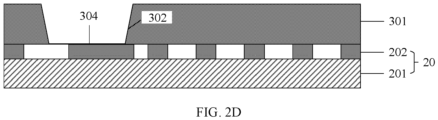
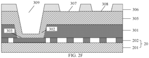
- FIG. 2A to FIG. 2G are cross-sectional diagrams of structures during a manufacturing process of an package structure provided by an embodiment of the disclosure
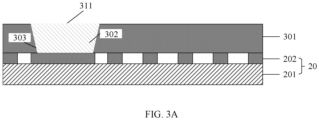
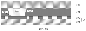
- FIG. 3A to FIG. 3B are cross-sectional diagrams of structures during a manufacturing process of a conductive pillar provided by an embodiments of the disclosure
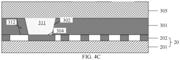
- FIG. 4A to FIG. 4C are cross-sectional diagrams of structures during a manufacturing process of another package structure provided by an embodiments of the disclosure.
- the method for manufacturing an package structure provided by the embodiment of the disclosure will be described in detail below with reference to FIG. 1 , FIG. 2A to FIG. 2G , FIG. 3A to FIG. 3C and FIG. 4A to FIG. 4D .
- a semiconductor functional structure 20 is provided.
- providing the semiconductor functional structure 20 includes providing a substrate (not shown in FIG. 2A ), in which a semiconductor functional layer 201 is provided on the substrate, and an interconnecting layer 202 is provided on the semiconductor functional layer 201.
- the material constituting the substrate may include silicon (Si), germanium (Ge), silicon germanium (SiGe) or the like.
- the material of the substrate may also include a silicon-on-insulator (SOI) or a germanium-on-insulator (GOI).
- the semiconductor functional layer 201 includes a monolayer thin film or multilayer thin films.
- the semiconductor functional layer 201 has a conductive layer and/or a dielectric layer.
- multiple microstructure layers may be provided in the semiconductor functional layer 201, in which formation methods of the various microstructure layers may be the same or different.
- a process for forming the semiconductor functional layer 201 includes but is not limited to a process of epitaxis, deposition, etching, polishing and grinding, or the like.
- the interconnecting layer 202 can be used for electrically connecting electrical signals of the semiconductor functional layer 201 with other interconnecting structures (for example, a conductive pillar, a interconnecting layer, etc.) and may also be used for playing a supporting role.
- the interconnecting layer may include a top metal layer.
- the material of the interconnecting layer includes, but is not limited to copper (Cu).
- the interconnecting layer 202 may be formed on the semiconductor functional layer 201 by a process of physical vapor deposition (PVD), chemical vapor deposition (CVD), atomic layer deposition (ALD), or the like.
- PVD physical vapor deposition
- CVD chemical vapor deposition
- ALD atomic layer deposition
- any signal connected by the redistribution layer formed in the subsequent manufacturing process is connected to the interconnecting layer 202, that is, the function of the semiconductor functional structure 20 is guaranteed to be complete even without the redistribution layer.
- parts of the interconnecting layer 202 are removed before forming the isolation layer 301 to reduce the total area of the interconnecting layer corresponding to the redistribution layer.
- the removed parts of the interconnecting layer 202 are the parts that are not physically connected to other interconnecting structures.
- the process for removing the part of the interconnecting layer 202 includes, but is not limited to an etching process.
- reducing the total area of the interconnecting layer is equivalent to reduction of an area of a electrode of the parasitic capacitance formed by the interconnecting layer and the redistribution layer, so that the reduction of the total area of the interconnecting layer 202 is beneficial to reducing additional parasitic capacitance caused by the interconnecting layer 202.
- FIG. 2B shows a cross-sectional diagram of a partial section after parts of the interconnecting layer 202 are removed.
- the parts of the interconnecting layer are not separated, but interconnected, that is, from another cross section view, the parts of the interconnecting layer are continuous.
- the first pad for performing a first type test is formed.
- the isolation layer 301 is formed on the interconnecting layer 202.
- the isolation layer 301 is used to protect the interconnecting layer 202 from being damaged.
- the material of the isolation layer 301 includes, but is not limited to, tetraethyl orthosilicate (TEOS).
- a process for forming the isolation layer 301 includes, but is not limited to, a process of PVD, CVD, ALD or the like.
- a part region of the isolation layer 301 is removed so that the isolation layer 301 has a plurality of via holes 302.
- Each via hole 302 exposes part of the interconnecting layer 202, and the exposed part of the interconnecting layer 202 acts as the first pad 303.
- the via hole 302 may have a shape of a cylinder or an inverted trapezoid or any suitable shapes.
- a cross-sectional area of the via hole includes an area of the orthographic projection of the via hole 302 on the plane where the interconnecting layer is located.
- the cross-sectional area of the first pad 303 is the smallest cross-sectional area of the via hole 302.
- the first pad 303 can be used for performing the first type test; on the other hand, it can be used for executing functional interactions corresponding to contents of the first type test.
- the first type test can be understood as some tests performed on the semiconductor functional structure when a running speed is low.
- a running speed refers to the reading or writing speed of the memory.
- the first pad 303 can be used to contact with a probe card to realize an electrical connection between the interconnecting layer and other test systems when performing the first type test, and can also be used for leading out a bonding wire which is electrically connected to the interconnecting layer 202 by the first pad 303.
- windowing region that is, the area of the first pad
- the redistribution layer windowing manner there is only a limitation of the minimum area of the region connected to the interconnecting layer.
- the large top metal layer prepared for windowing can be tailored, provided that it meets the design requirements.
- the first pad can be cut to reduce its area to a minimum area as long as it satisfies the connection between the redistribution layer an the interconnecting layer.
- part of the first pad 303 is removed to form a fourth pad 304.
- the area of the fourth pad 304 is smaller than an area of the first pad 303.
- the removed part of the interconnecting layer 202 is the part of the first pad 303, and the remaining part of the first pad 303 is the fourth pad 304.
- the area of the first pad 303 is slightly greater than a cross-sectional area of the via hole 302, and the area of the fourth pad 304 is apparently less than the cross-sectional area of the via hole 302. Based on this, it can be understood that the area of fourth pad 304 is less than the cross-sectional area of the via hole 302.
- the first pad 303 and the fourth pad 304 have other forms.
- the area of the first pad 303 is reduced to the area of the fourth pad 304, and the parasitic capacitance of a semiconductor device is decreased by 5.3%.
- FIG. 2E shows corresponding top views of FIG. 2C and FIG. 2D .
- whether to reduce the area of the first pad to the area of the fourth pad can be selected according to actual requirements. It is preferred to reduce the area of first pad to the area of fourth pad.
- a redistribution layer 305 is formed.
- completing the first type test includes performing and passing the first type test. Passing the first type test includes that a result of the first type test meets the preset conditions.
- the preset conditions can be understood as the test requirements set for the semiconductor functional structure 20 according to actual requirements.
- the redistribution layer 305 is formed on the first pad 303 and the isolation layer 301.
- the redistribution layer 305 and the interconnecting layer 202 are electrically connected.
- the subsequent process of the packaging method provided by the embodiment of the disclosure for the further manufacture may not be carried out, and the tested semiconductor functional structure 20 is adjusted until a result of the first type test meets the preset condition, and then the subsequent process of the packaging method provided by the embodiment of the disclosure for the further manufacture is carried out.
- the material constituting the redistribution layer 305 includes, but is not limited to, a metal.
- the material of the redistribution layer is aluminum (Al).
- a specific manner of forming the redistribution layer 305 includes: forming a new wire pattern on the isolation layer 301 in an exposure and development manner, and then forming the redistribution layer 305 according to the new wire pattern by an electroplating technique.
- the redistribution layer 305 includes new wire paths, which are electrically connected to the interconnecting layer 202.
- forming the redistribution layer on the first pad and the isolation layer includes: forming the redistribution layer 305 on the first pad 303 and the isolation layer 301 by a maskless deposition process.
- the maskless deposition process can be understood as forming the redistribution layer 305 directly on the first pad 303 and the isolation layer 301 without forming a mask.
- adopting the maskless deposition process can not only save costs of a mask plate and a manufacturing equipment thereof, but also improves flexibility of the deposition process and improves the production efficiency, thereby shortening the production cycle and reducing the manufacturing costs.
- a first insulating layer 306 is formed on the redistribution layer 305.
- the first insulating layer 306 covers the redistribution layer to protect the redistribution layer 305 from being damaged. In addition, parts of the first insulating layer 306 are removed, to expose parts of the redistribution layer 305.
- the material of the first insulating layer 306 includes, but is not limited to, polyimide (PI).
- a process for forming the first insulating layer 306 includes, but is not limited to, a PVD process, a CVD process, an ALD process or the like.
- the removal process includes, but is not limited to, an etching process or the like.
- the first insulating layer 306 not only exposes parts of the redistribution layer to form a second pad 307 and a third pad 308, but also exposes the redistribution layer 305 located on the first pad 303, such that a second insulating layer is filled in a groove formed by the redistribution layer 305 subsequently.
- the density of the second insulating layer may be equal to or less than the density of the first insulating layer 306.
- the first insulating layer 306 also covers the bottom surface and the sidewalls of the groove formed by the redistribution layer 305, and the second insulating layer is subsequently formed in a groove formed by the first insulating layer 306.
- the exposed parts of the redistribution layer include the second pad 307 and the third pad 308.
- the second pad 307 is used for performing a second type test
- the third pad 308 is used for executing a functional interaction corresponding to the contents of the second type test.
- the second type test can be understood as some tests performed on the semiconductor functional structure when the running speed is high. Executing a functional interaction corresponding to the contents of the second type test can be understood as leading out a bonding wire from the third pad.
- positions of the second pad 307 and the third pad 308 can be selected and disposed according to actual requirements.
- the redistribution layer 305 and the interconnecting layer 202 are electrically connected to lead out the electrical signals of the semiconductor functional structure 20. Then, windowing positions of the second pad 307 and the third pad 308 are disposed according to actual requirements. Next, the electrical test and the functional interaction thereof are performed on the semiconductor functional structure 20 by the second pad 307 and the third pad 308.
- the redistribution layer 305 is used to redistribute wire paths based on the layout of the wire paths of the first pad 303.
- the redistributed wire paths are more conducive to the electrical test and functional interaction thereof of the semiconductor device.
- the second pad 307 is located at a side close to an edge of the semiconductor functional structure; and the third pad 308 is located at a side away from the edge of the semiconductor functional structure.
- controllability or adjustability of a process for leading out the bonding wire on the pad is relatively flexible, and a process for aligning the pad with the probe card is relatively difficult.
- the second pad 307 is disposed at a side close to the edge of the semiconductor functional structure; it is beneficial to reducing the difficulty of aligning the pad and the probe card, thereby reserving more flexibility for the probe card during performing the test.
- the second pad 307 is located at a side away from the edge of the semiconductor functional structure, and the third pad 308 is located at a side close to the edge of the semiconductor functional structure.
- the groove 309 is provided in the middle region of the redistribution layer 305 on the first pad 303.
- the method further includes forming a second insulating layer 310 in the groove 309 enclosed with the redistribution layer.
- a hardness of the material of the second insulating layer 310 is less than a hardness of the material of the redistribution layer 305.
- the hardness of the material of the second insulating layer 310 is smaller, on the one hand, it is beneficial to reduce the stress of the package structure, and increase the reliability; on the other hand, compared to the case of filling the groove with the redistribution layer, filling the groove 309 with the material of the second insulating layer 310 can avoid generating greater parasitic capacitance.
- the material constituting the second insulating layer 310 includes, but is not limited to, polyimide (PI).
- a process for forming the second insulating layer 310 includes, but is not limited to, a process of PVD, CVD, ALD or the like.
- materials of the second insulating layer 310 and the first insulating layer 306 may be the same.
- the second insulating layer 310 may be formed in the same operation for forming the first insulating layer 306.
- the second insulating layer 310 and the first insulating layer 306 are an integrated structure.
- the redistribution layer 305 is formed directly on the first pad 303 and the isolation layer 301 by the maskless deposition process, so that the redistribution layer 305 and the first pad 303 are electrically conductive by a physical contact manner.
- the redistribution layer 305 and the first pad 303 are electrically conductive by a conductive pillar. This manner is described in detail with reference to FIG. 3A , FIG. 3B and FIG. 3C .
- the method further includes the following operations.
- a conductive pillar 311 is formed on the first pad 303; and forming the redistribution layer 305 on the first pad 303 and the isolation layer 301 includes: forming the redistribution layer 305 on the conductive pillar 311 and the isolation layer 301.
- the redistribution layer 305 and the interconnecting layer 202 are electrically connected by the conductive pillar 311.
- the material of the conductive pillar 311 and the material of the redistribution layer 305 may be the same or different. It should be noted that the height of the conductive pillar 311 may be equal to or less than the depth of the via hole 302, and FIG. 3A shows the case that the height of the conductive pillar 311 is equal to the depth of the via hole 302.
- the material constituting the conductive pillar 311 includes Al, copper (Cu) or the like.
- a process for forming the conductive pillar includes, but is not limited to, a process of PVD, CVD, ALD or the like.
- the redistribution layer 305 is formed on the first pad 303 and the isolation layer 301.
- the redistribution layer 305 and the interconnecting layer 202 are electrically connected by the conductive pillar 311.
- a first insulating layer 306 is formed on the redistribution layer 305, and parts of the first insulating layer 306 are removed, exposing parts of the redistribution layer 305.
- the exposed parts of the redistribution layer 305 include a second pad 307 and a third pad 308.
- the second pad 307 is used for performing a second type test
- the third pad 308 is used for executing the functional interaction corresponding to the contents of the second type test.
- positions of the second pad 307 and the third pad are selected and disposed according to actual requirements.
- the conductive pillar 311 is formed on the surface of the fourth pad 304.
- the deposition process may be performed by using the mask for etching the first pad 303 to form the fourth pad 304, to form a third insulating layer 312 filling part of the via hole 302, and after the third insulating layer 311 is formed, the conductive pillar 311 is formed, filling up the via hole 302.
- the material of the third insulating layer 312 includes, but is not limited to, polyimide (PI).
- a process for forming the third insulating layer 312 includes, but is not limited to, a process of PVD, CVD, ALD or the like.
- the redistribution layer 305 is formed on the conductive pillar 311 and the isolation layer 301.
- the conductive pillar 311 is located between the fourth pad 304 and the redistribution layer 305, and the redistribution layer 305 and the interconnecting layer 202 are electrically connected by the conductive pillar 311.
- FIG. 4C shows the cross-sectional diagram where the conductive pillar 311 has filled part of the via hole 302.
- the conductive pillar 311 may also be disposed with other shapes or at other positions.
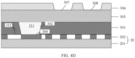
- a first insulating layer 306 is formed on the redistribution layer 305, and parts of the first insulating layer 306 are removed, exposing parts of the redistribution layer 305.
- the exposed parts of the redistribution layer 305 include a second pad 307 and a third pad 308.
- the second pad 307 is used for performing a second type test
- the third pad 308 is used for executing the functional interaction corresponding to the contents of the second type test.
- positions of the second pad 307 and the third pad can be selected and disposed according to actual requirements.
- each conductive pillar 311 formed in the same via hole 302 in the above embodiment may be one or more. Accordingly, each conductive pillar 311 corresponds to a fourth pad 304, that is, when the number of conductive pillar 311 is more than one, a plurality of fourth pad 304 are provided at the bottom of the same one via hole 302.
- the multiple conductive pillars 311 are respectively connected to the redistribution layer 305 and the interconnecting layer 202, so that reliability of the electrical connection between the redistribution layer 305 and the interconnecting layer 202 can be increased.
- the other conductive pillars can connect the redistribution layer and the interconnecting layer, thereby improving the reliability of the electrical connection between the redistribution layer, the conductive pillars and the interconnecting layer.
- the first pad is disposed on the semiconductor functional structure, which is used for performing the first type test when the running speed of the semiconductor functional structure is low,; after completing the first type test, the redistribution layer and the insulating layer are formed on the first pad to further form the second pad and the third pad, and the second pad is used for performing the second type test when the running speed of the semiconductor functional structure is high, and the third pad is used for executing the functional interaction corresponding to the contents of the second type test.
- the package structure compatible with the two types of tests is adopted in the disclosure, so that the semiconductor functional structure is satisfied with different types of tests in different process stages, thereby improving flexibility of testing, shortening the production cycle and reducing the manufacturing costs.
- embodiments of the disclosure further provide a package structure, including: an isolation layer with a via hole, a fourth pad, a redistribution layer and a first insulating layer.
- the isolation layer covers a surface of an interconnecting layer, the via hole exposes part of the interconnecting layer, and the interconnecting layer is disposed on a surface of a semiconductor functional structure.
- the fourth pad consists of the interconnecting layer exposed by the isolation layer, an area of the fourth pad is less than a cross-sectional area of the via hole, and the cross-sectional area of the via hole is set according to requirements of a first type test.
- the redistribution layer covers the isolation layer and is electrically connected with the fourth pad.
- the first insulating layer covers and exposes parts of the redistribution layer.
- the exposed parts of the redistribution layer include a second pad and a third pad.
- the second pad is used for performing a second type test
- the third pad is used for executing a functional interaction corresponding to contents of the second type test.
- a running speed of the semiconductor functional structure when performing the first type test is lower than a running speed when performing the second type test.
- the package structure further includes a conductive pillar.
- the conductive pillar is located between the fourth pad and the redistribution layer, and the redistribution layer and the interconnecting layer are electrically connected by the conductive pillar.
- the number of the conductive pillar is one or more.
- the package structure further includes: a second insulating layer.
- the second insulating layer is located in a groove surrounded the redistribution layer.
- a hardness of a material of the second insulating layer is less than a hardness of a material of the redistribution layer.
- the second pad is located at a side close to an edge of the semiconductor functional structure; and the third pad is located at a side away from the edge of the semiconductor functional structure.
- embodiments of the disclosure further provide a semiconductor device, including: the package structure described in the foregoing embodiments of the disclosure.
- the semiconductor device further includes: a substrate and a plurality of bare chips.
- each die includes a semiconductor functional structure and the package structure located on the semiconductor functional structure.
- Each die is electrically connected to the substrate by a lead on a third pad of the package structure.
- the package structure compatible with the two types of tests is adopted, so that the semiconductor functional structure can satisfied with the different types of tests in different manufacture procedure stages.
- the position of the via hole of the redistribution layer needs to be reserved on the top metal layer to ensure that when the redistribution layer needs to be added, it is not necessary to modify the top metal layer or any photolithography plate and the process.
- the layout design it is necessary to consider the layout of the top metal layer and its windowing (such as, the interconnecting layer and the first pad) and the layout of the redistribution layer and its windowing (the second pad and the third pad) at the same time.
- the two windowing regions cannot be opened at the same time.
- a semiconductor device layout structure including: a semiconductor functional structure layout layer 501 and a package structure layout layer 502 which are stacked.
- the package structure layout layer 502 includes a plurality of first type pad regions 5021, in which each first type pad region includes a partial interconnecting layer region 5021a and a first pad region5021b located in the partial interconnecting layer region 5021b; a plurality of conductive pillar regions 5022, in which each conductive pillar region is located on a corresponding first type pad region; and a plurality of second type pad regions 5023, in which each second type pad region is located on a corresponding conductive pillar region of the first type pad region, and includes: a redistribution layer region 5023a, and a second pad region 5023b and a third pad region 5023c located in the redistribution layer region.
- An orthographic projection of the first pad region on a preset plane and an orthographic projection of the redistribution layer region on the preset plane have an overlapping region, an orthographic projection of the conductive pillar region on the preset plane is located in the overlapping region, and the preset plane is perpendicular to the stacking direction.
- embodiments of the disclosure also provide an application method of the semiconductor device layout structure, which includes: by utilizing the semiconductor device layout structure described in the above embodiments of the disclosure, forming a semiconductor functional structure and a plurality of first type pads, or forming a semiconductor functional structure, a plurality of first type pads, and a plurality of second type pads.
- the layout of the top metal layer windowing (the first type pad regions) and the layout of the redistribution layer windowing (the second type pad regions) are designed at the same time, but the two windowing correspond to different layout levels or photolithography plates, that is, it is guaranteed that two windowing regions cannot be opened at the same time. That is, the semiconductor functional structure, the plurality of first type pads, the plurality of second type pads and their corresponding layout structures illustrated in the embodiments of the disclosure can be used separately.
- the disclosed devices and methods may be implemented in a non-target way.
- the above-described device embodiments are only schematic.
- the division of the units is only a logical function division, and there may be other division modes in actual implementation, such as, multiple units or components may be combined or integrated into another system, or some features may be omitted or not executed.
- the components shown or discussed may be coupled, or directly coupled to each other.
- the units described above as separate parts may or may not be physically separate, and the parts shown as a unit may or may not be a physical units, that is, they may be located in one place or distributed to multiple network units. Some or all of the units may be selected according to actual requirements to achieve the purpose of the solutions of the embodiments of the disclosure.
- a package structure compatible with two types of tests is adopted in the disclosure, so that a semiconductor functional structure can be subjected to different types of tests in different process stages, thereby improving flexibility of testing, shortening the production cycle and reducing the manufacturing costs.
Landscapes
- Internal Circuitry In Semiconductor Integrated Circuit Devices (AREA)
- Engineering & Computer Science (AREA)
- Manufacturing & Machinery (AREA)
- Automation & Control Theory (AREA)
- Testing Or Measuring Of Semiconductors Or The Like (AREA)
Abstract
Description
- This application is based on and claims priority to
Chinese Patent Application No.202210621408.5, filed on June 01, 2022 - The disclosure relates to a technical field of semiconductors, particularly to, but is not limited to a package structure, a packaging method and a semiconductor device.
- With the rapid increase in the popularity rate of electronic equipment and the vigorous development of the electronic equipment market, electronic products are increasingly required to evolve towards miniaturization and thinness while having a high performance, multifunctionality, high reliability and convenience. Such requirements put forward better, lighter, thinner, higher package density, better electrical and thermal properties, higher reliability and higher cost performance requirements for packaging of semiconductor devices.
- In order to ensure the performance of a semiconductor device to meet corresponding requirements, it is necessary to prepare ports for testing and executing functional interactions on a package structure.
- Based on this, in order to solve one or more problems of the related art, embodiments of the disclosure provide a package structure, a packaging method and a semiconductor device.
- According to embodiments of the disclosure, a packaging method is provided, including the following operations.
- A semiconductor functional structure is provided, in which an interconnecting layer is disposed on a surface of the semiconductor functional structure;
- An isolation layer exposing part of the interconnecting layer is formed, in which the exposed part of the interconnecting layer acts as a first pad, and the first pad is used for performing a first type test;
- A redistribution layer is formed on the first pad and the isolation layer, in which the redistribution layer and the interconnecting layer are electrically connected after completing the first type test.
- A first insulating layer exposing part of the redistribution layer is formed, in which the exposed parts of the redistribution layer act as a second pad and a third pad, and the second pad is used for performing a second type test, and the third pad is used for executing a functional interaction corresponding to contents of the second type test. A running speed of the semiconductor functional structure when performing the first type test is lower than a running speed of the semiconductor functional structure when performing the second type test.
- In the above solutions, the method further includes the following operation.
- Part of the interconnecting layer is removed to reduce a total area of the interconnecting layer corresponding to the redistribution layer before forming the isolation layer.
- In the above solutions, the method further comprises the following operation.
- Part of the first pad is removed to form a fourth pad after completing the first type test, in which an area of the fourth pad is smaller than an area of the first pad.
- In the above solutions, forming the redistribution layer on the first pad and the isolation layer includes the following operation.
- The redistribution layer is formed on the first pad and the isolation layer by a maskless deposition process.
- The method further includes the following operation.
- A second insulating layer is formed in a groove surrounded by the redistribution layer, in which a hardness of a material of the second insulating layer is less than a hardness of a material of the redistribution layer.
- In the above solutions, the method further includes the following operation.
- A conductive pillar is formed on the first pad after completing the first type test.
- The operation of forming the redistribution layer on the first pad and the isolation layer includes the following operation.
- The redistribution layer is formed on the conductive pillar and the isolation layer, in which the redistribution layer and the interconnecting layer are electrically connected by the conductive pillar.
- According to embodiments of the disclosure, a package structure is provided. The package structure includes: an isolation layer with a via hole, a fourth pad, a redistribution layer and a first insulating layer.
- The isolation layer covers a surface of an interconnecting layer, the via hole exposes part of an interconnecting layer, and the interconnecting layer is disposed on a surface of a semiconductor functional structure.
- The fourth pad consists of the interconnecting layer exposed by the isolation layer, an area of the fourth pad is less than a cross-sectional area of the via hole, and the cross-sectional area of the via hole is disposed according to requirements of a first type test.
- The redistribution layer covers the isolation layer and is electrically connected with the fourth pad.
- The first insulating layer covers the redistribution layer and exposes parts of the redistribution layer.
- The exposed parts of the redistribution layer include a second pad and a third pad, the second pad is used for performing a second type test, and the third pad is used for executing a functional interaction corresponding to contents of the second type test. A running speed of the semiconductor functional structure when performing the first type test is lower than a running speed of the semiconductor functional structure when performing the second type test.
- In the above solutions, the package structure further includes a conductive pillar, located between the fourth pad and the redistribution layer, in which the redistribution layer and the interconnecting layer are electrically connected by the conductive pillar.
- In the above solutions, a number of the conductive pillar is one or more.
- In the above solutions, the package structure further includes a second insulating layer located in a groove surrounded by the redistribution layer, in which a hardness of a material of the second insulating layer is less than a hardness of a material of the redistribution layer.
- In the above solutions, the second pad is located at a side close to an edge of the semiconductor functional structure; and the third pad is located at a side away from the edge of the semiconductor functional structure.
- According to embodiments of the disclosure, a semiconductor device is provided. The semiconductor device includes the package structure described in the foregoing embodiments of the disclosure.
- In the above solutions, the semiconductor device further includes: a substrate; and a plurality of bare chips.
- The plurality of dies are stacked, in which each die comprises a semiconductor functional structure and a package structure located on the semiconductor functional structure, and each die is electrically connected to the substrate by a lead on a third pad of the package structure.
- In the embodiments of the disclosure, the first pad is disposed in the semiconductor functional structure, which is used for performing the first type test when the semiconductor functional structure's running speed is low; after completing the first type test, the redistribution layer and the insulating layer are formed on the first pad to further form the second pad and the third pad, and the second pad is used for performing the second type test when the semiconductor functional structure's running speed is high, and the third pad is used for executing the functional interaction corresponding to the contents of the second type test. In this way, the package structure compatible with the two types of tests adopted in the disclosure can satisfy the semiconductor functional structure subjecting to different types of tests in different process stages, thereby improving flexibility of testing, shortening production cycle and reducing manufacturing costs.
-
-
FIG. 1 is a schematic flowchart of a method for manufacturing a package structure provided by an embodiment of the disclosure; -
FIG. 2A to FIG. 2G are cross-sectional schematic diagrams during a manufacturing process of an package structure provided by an embodiment of the disclosure; -
FIG. 3A to FIG. 3B are cross-sectional schematic diagrams during a manufacturing process of a conductive pillar provided by an embodiments of the disclosure; -
FIG. 4A to FIG. 4D are cross-sectional schematic diagrams during a manufacturing process of another package structure provided by an embodiment of the disclosure; and -
FIG. 5 is a schematic top view of a layout structure of a semiconductor device provided in an embodiment of the disclosure. - 20, semiconductor functional structure; 201, semiconductor functional layer; 202, interconnecting layer; 301, isolation layer; 302, via hole; 303, first pad; 304, fourth pad; 305, redistribution layer; 306, first insulating layer; 307, second pad; 308, third pad; 309, groove; 310, second insulating layer; 311, conductive pillar; 312, third insulating layer; 501, semiconductor functional structure layout layer; 502, package structure layout layer; 5021, first type pad region; 5021a, partial interconnecting layer region; 5021b, first pad region; 5022, conductive pillar region; 5023, second type pad region; 5023a, redistribution layer region; 5023b, second pad region; and 5023c, third pad region.
- In the above drawings (which are not necessarily drawn to scale), similar reference numerals may describe similar parts in different views. Similar reference numerals with different letter suffixes may represent similar parts in different examples. The various embodiments discussed herein are generally shown in the accompanying drawings by way of example, but not limitation.
- The technical solutions of the disclosure will be further described in detail below with reference to the drawings and embodiments. While exemplary implementing modes of the disclosure are shown in the drawings it should be understood that the disclosure may be implemented in various forms and should not be limited by the embodiments set forth herein. In contrast, these embodiments are provided to enable a more thorough understanding of the disclosure and to fully convey the scope of the disclosure to a person skilled in the art.
- The embodiments of the disclosure are described in more detail by way of example in the following paragraphs with reference to the drawings. The advantages and features of the disclosure will become clearer according to the following descriptions and claims. It should be noted that the accompanying drawings are all in very simplified forms and in inaccurate scales, and are only used to facilitate and clearly assist the purpose of explaining the embodiments of the disclosure.
- It is understood that the meanings of "on", "above" and "over" of the disclosure should be interpreted in the widest manner so that "on" not only means that it is "on" something without an intervening feature or layer being in between (i.e. directly on something), but also includes that it is "above" something with an intervening feature or layer being in between.
- In the embodiments of the disclosure, the term "A is connected to B" includes the situation that A and B are in direct contact, and the situation that A and B are indirectly in contact through an intermediate conductive structure.
- In the embodiments of the disclosure, the terms "first "and "second", etc. are used to distinguish similar objects and are not necessarily used to describe a specific order or sequence.
- In the embodiments of the disclosure, the term "layer" refers to part of material that includes a region having a thickness. A layer may extend over a surface of a lower or upper structure, or may have an area smaller than an extent of the lower or upper structure. Furthermore, a layer may be a region of a homogeneous or heterogeneous continuous structure, having a thickness less than the thickness of the continuous structure. For example, a layer may be between a top surface and the bottom surface of a continuous structure, or the layer may be between any horizontal planes at the top and bottom surfaces of a continuous structure. A layer may extend horizontally, vertically and/or along an inclined surface. A layer may include multiple sub-layers. For example, an interconnection layer may include one or more conductors and contact sub-layers (in which interconnecting wires and/or via hole contacts are formed), and one or more dielectric sub-layers.
- It should be noted that technical solutions described in the embodiments of the disclosure can be arbitrarily combined as long as there is no conflict.
- A semiconductor functional structure described in the embodiments of the disclosure is used for subsequent processes and forms part of a final semiconductor device, and is a core part to realize a main function of the semiconductor device. Here, the final semiconductor device may include, but is not limited to a memory.
- In a design of a packaging structure of a semiconductor device, such as a dynamic random access memory (DRAM), a pad (also called bonding pad) can be disposed in two manners: one is top metal layer windowing, and the other is redistribution layer (RDL) windowing.
- The top metal layer windowing refers to that a passivation layer or an insulating layer is formed on a top metal layer of the semiconductor functional structure to protect the semiconductor functional structure from being damaged, and then a windowing region is formed in the passivation layer or the insulating layer to expose part of the top metal layer and thus form the pad. A prode card sticking test may be carried out on the pad to realize an electrical property test of the semiconductor functional structure, and a bonding wire may be leaded out from the pad to realize an electrical leading out of the semiconductor functional structure.
- The redistribution layer windowing refers to that a redistribution layer is formed on a top metal layer of the semiconductor functional structure, and a passivation layer or an insulating layer is formed on the redistribution layer, and then a windowing region is formed in the passivation layer or the insulating layer to expose part of the redistribution layer and thus form two pads arranged side by side. One of the two pads is used for performing a probe card sticking test, and the other pad is used for leading out a bonding wire therefrom. Here, the redistribution layer can play a role of adjusting a position of a pad in a semiconductor device, and can also play a role of enhancing a power supplying network of a power ground.
- Understandably, the top metal layer is relatively thin, and there is a gasket structure below it, which can support the probe card sticking test first, and then the bonding wire packaging in a packaging factory on the same windowing metal region without affecting the yield of packaging and wiring. The material of the redistribution layer is generally a metal, and the redistribution layer is thicker than the top metal layer, and thus there are usually deep and rough sticking traces on the surface after the probe card sticking test. Such sticking traces may affect the yield of packaging and wiring. Therefore, in the redistribution layer, the pad used for testing and the pad used for leading out bonding wires are different. No matter which of the above windowing manners is adopted in a package structure, it has little influence on the function of a semiconductor device. The redistribution layer windowing is beneficial to improving the performance, but it increases the production cycle and production cost.
- In the related art, one of the above two windowing manners is generally selected to design a package structure according to an actual requirement of a semiconductor device. However, in practical applications, in a production process of semiconductor devices, the requirement is no single, and there are often multiple requirements. Here are several examples of such multiple requirements.
- Exemplarily, before a mass production of a semiconductor device (or referred to as "product"), there is a long term of the functional debugging process. In the debugging process, a test is completed with a low running speed of a semiconductor functional structure. In this situation, only the top metal windowing is needed to be adopted to complete the packaging and the testing of the semiconductor functional structure. However, when the manufacturing process of the product is mature and it is necessary to test the semiconductor functional structure under a state of running at a high speed, the redistribution layer windowing is needed to be adopted for a packaging test.
- Exemplarily, when a semiconductor functional structure itself has different functional demands, a test for the same semiconductor functional structure can be classified into a standard grade test and an advanced grade test according to different demands. The requirements for windowing modes of the different test grades of the semiconductor functional structure are also different. When the standard grade test is performed on the semiconductor functional structure, the top metal layer windowing can be adopted for the packaging and testing, and the role of a redistribution layer is not apparent. When the advanced grade test is performed on the semiconductor functional structure, the redistribution layer windowing is needed to be adopted for the packaging and testing, to improve the performance of the product.
- To sum up, in the related art, adopts one of the two windowing manners in a package structure of a semiconductor functional structure cannot meet different test demands to the semiconductor functional structure of a semiconductor device during different manufacturing process stages. In view of this, in order to solve at least one of the above problems, the embodiments of disclosure provides a package structure, a packaging method and a semiconductor device, which are compatible with the two types of tests, meet the requirements that a semiconductor functional structure can be subjected to different types of tests in different manufacturing process stages, improve flexibility of testing, shorten the production cycle and reduce manufacturing cost.
-
FIG. 1 is a schematic flowchart of a method for manufacturing a package structure provided by an embodiment of the disclosure. As shown inFIG. 1 , a method for manufacturing a package structure provided by an embodiment of the disclosure includes the following operations. - At S101, a semiconductor functional structure is provided, in which an interconnecting layer is disposed on a surface of the semiconductor functional structure.
- At S102, an isolation layer exposing part of the interconnecting layer is formed, in which the exposed part of the interconnecting layer acts as a first pad, and the first pad is used for performing a first type test.
- At S103, after completing the first type test, a redistribution layer is formed on the first pad and the isolation layer, in which the redistribution layer and the interconnecting layer are electrically connected.
- At S104, a first insulating layer exposing parts of the redistribution layer is formed, in which the exposed parts of the redistribution layer act as a second pad and a third pad, respectively, the second pad is used for performing a second type test, and the third pad is used for executing a functional interaction corresponding to contents of the second type test; and a running speed of the semiconductor functional structure when performing the first type test is lower than a running speed when performing the second type test.
- It should be understood that the operations shown in
FIG. 1 are not exclusive and that other operations may be performed before, after, or between any of the operations; and the order of the operations shown inFIG. 1 can be adjusted according to actual requirements.FIG. 2A to FIG. 2G are cross-sectional diagrams of structures during a manufacturing process of an package structure provided by an embodiment of the disclosure;FIG. 3A to FIG. 3B are cross-sectional diagrams of structures during a manufacturing process of a conductive pillar provided by an embodiments of the disclosure; andFIG. 4A to FIG. 4C are cross-sectional diagrams of structures during a manufacturing process of another package structure provided by an embodiments of the disclosure. The method for manufacturing an package structure provided by the embodiment of the disclosure will be described in detail below with reference toFIG. 1 ,FIG. 2A to FIG. 2G ,FIG. 3A to FIG. 3C andFIG. 4A to FIG. 4D . - At S101, a semiconductor
functional structure 20 is provided. - Referring to
FIG. 2A , providing the semiconductorfunctional structure 20 includes providing a substrate (not shown inFIG. 2A ), in which a semiconductorfunctional layer 201 is provided on the substrate, and aninterconnecting layer 202 is provided on the semiconductorfunctional layer 201. - Here, the material constituting the substrate may include silicon (Si), germanium (Ge), silicon germanium (SiGe) or the like. In other embodiments, the material of the substrate may also include a silicon-on-insulator (SOI) or a germanium-on-insulator (GOI).
- The semiconductor
functional layer 201 includes a monolayer thin film or multilayer thin films. The semiconductorfunctional layer 201 has a conductive layer and/or a dielectric layer. According to actual requirements, multiple microstructure layers may be provided in the semiconductorfunctional layer 201, in which formation methods of the various microstructure layers may be the same or different. Based on this, a process for forming the semiconductorfunctional layer 201 includes but is not limited to a process of epitaxis, deposition, etching, polishing and grinding, or the like. - The interconnecting
layer 202 can be used for electrically connecting electrical signals of the semiconductorfunctional layer 201 with other interconnecting structures (for example, a conductive pillar, a interconnecting layer, etc.) and may also be used for playing a supporting role. In some embodiments, the interconnecting layer may include a top metal layer. In some specific embodiments, the material of the interconnecting layer includes, but is not limited to copper (Cu). - Here, the interconnecting
layer 202 may be formed on the semiconductorfunctional layer 201 by a process of physical vapor deposition (PVD), chemical vapor deposition (CVD), atomic layer deposition (ALD), or the like. - It should be noted that any signal connected by the redistribution layer formed in the subsequent manufacturing process is connected to the interconnecting
layer 202, that is, the function of the semiconductorfunctional structure 20 is guaranteed to be complete even without the redistribution layer. - In some embodiments, referring to
FIG. 2B , parts of the interconnectinglayer 202 are removed before forming theisolation layer 301 to reduce the total area of the interconnecting layer corresponding to the redistribution layer. - Here, the removed parts of the interconnecting
layer 202 are the parts that are not physically connected to other interconnecting structures. The process for removing the part of the interconnectinglayer 202 includes, but is not limited to an etching process. - Understandably, considering that parasitic capacitance may be introduced with the introduction of the redistribution layer to the large area where the top metal layer is windowed in a subsequent process, reducing the total area of the interconnecting layer is equivalent to reduction of an area of a electrode of the parasitic capacitance formed by the interconnecting layer and the redistribution layer, so that the reduction of the total area of the interconnecting
layer 202 is beneficial to reducing additional parasitic capacitance caused by the interconnectinglayer 202. - It should be noted that
FIG. 2B shows a cross-sectional diagram of a partial section after parts of the interconnectinglayer 202 are removed. In practical application, the parts of the interconnecting layer are not separated, but interconnected, that is, from another cross section view, the parts of the interconnecting layer are continuous. - At S102, the first pad for performing a first type test is formed.
- Specifically, referring to
FIG. 2C , theisolation layer 301 is formed on the interconnectinglayer 202. - Here, the
isolation layer 301 is used to protect theinterconnecting layer 202 from being damaged. The material of theisolation layer 301 includes, but is not limited to, tetraethyl orthosilicate (TEOS). A process for forming theisolation layer 301 includes, but is not limited to, a process of PVD, CVD, ALD or the like. - In the embodiment of the disclosure, a part region of the
isolation layer 301 is removed so that theisolation layer 301 has a plurality of viaholes 302. Each viahole 302 exposes part of the interconnectinglayer 202, and the exposed part of the interconnectinglayer 202 acts as thefirst pad 303. - Here, the via
hole 302 may have a shape of a cylinder or an inverted trapezoid or any suitable shapes. A cross-sectional area of the via hole includes an area of the orthographic projection of the viahole 302 on the plane where the interconnecting layer is located. However, it should be noted that when the viahole 302 has a shape of inverted trapezoid, the cross-sectional area of thefirst pad 303 is the smallest cross-sectional area of the viahole 302. - In practical application, on the one hand, the
first pad 303 can be used for performing the first type test; on the other hand, it can be used for executing functional interactions corresponding to contents of the first type test. - The first type test can be understood as some tests performed on the semiconductor functional structure when a running speed is low.
- It should be noted that in a memory, a running speed refers to the reading or writing speed of the memory.
- Here, the
first pad 303 can be used to contact with a probe card to realize an electrical connection between the interconnecting layer and other test systems when performing the first type test, and can also be used for leading out a bonding wire which is electrically connected to the interconnectinglayer 202 by thefirst pad 303. - On the one hand, it is understandable that due to the limitation of a test probe card and a pad of wire bonding package, there is a minimum area requirement for windowing region (that is, the area of the first pad) in the top metal layer windowing manner. While, in the redistribution layer windowing manner, there is only a limitation of the minimum area of the region connected to the interconnecting layer.
- On the other hand, considering that in the embodiment of the disclosure, both the top metal layer windowing manner and the redistribution layer windowing manner are adopted, a top metal layer and a redistribution layer respectively with a large area are inevitably required, either of which introduces additional parasitic capacitance. Exemplarily, the introduced additional parasitic capacitance is detrimental to high-speed ports of a low power double data rate (LPDDR).
- Based on this, after that the test at a low speed is stable (after first type test meets a preset condition) and the process is mature, it is necessary to start to debug the performance at a high speed, and pads of the redistribution layer are needed. In this case, the large top metal layer prepared for windowing can be tailored, provided that it meets the design requirements.
- After completing the first type test, the first pad can be cut to reduce its area to a minimum area as long as it satisfies the connection between the redistribution layer an the interconnecting layer.
- In view of this, in some embodiments, referring to
FIG. 2D , after completing the first type test, part of thefirst pad 303 is removed to form afourth pad 304. The area of thefourth pad 304 is smaller than an area of thefirst pad 303. - Here, the removed part of the interconnecting
layer 202 is the part of thefirst pad 303, and the remaining part of thefirst pad 303 is thefourth pad 304. As can be seen from the embodiment of the drawings, the area of thefirst pad 303 is slightly greater than a cross-sectional area of the viahole 302, and the area of thefourth pad 304 is apparently less than the cross-sectional area of the viahole 302. Based on this, it can be understood that the area offourth pad 304 is less than the cross-sectional area of the viahole 302. In other embodiments, thefirst pad 303 and thefourth pad 304 have other forms. - It is understandable that, by reducing the area of the
first pad 303, on one hand, additional parasitic capacitance caused by thefirst pad 303 can be reduced; on the other hand, parasitic resistance and electro-migration are reduced, thereby further meeting the production requirements. - Exemplarily, referring to
FIG. 2E , the area of thefirst pad 303 is reduced to the area of thefourth pad 304, and the parasitic capacitance of a semiconductor device is decreased by 5.3%. - It should be noted that
FIG. 2E shows corresponding top views ofFIG. 2C andFIG. 2D . - In an actual manufacturing process, whether to reduce the area of the first pad to the area of the fourth pad can be selected according to actual requirements. It is preferred to reduce the area of first pad to the area of fourth pad.
- However, in order to clearly describe the disclosure, in the following embodiments, description is made by taking the case that the first pad area is not reduced as an example. That is, in
FIG. 2F to FIG. 2G , the redistribution layer is still formed on the basis of the first pad. - At S103, referring to
FIG. 2F , after completing the first type test, aredistribution layer 305 is formed. - It should be noted that completing the first type test includes performing and passing the first type test. Passing the first type test includes that a result of the first type test meets the preset conditions. The preset conditions can be understood as the test requirements set for the semiconductor
functional structure 20 according to actual requirements. - Here, after the result of the first type test meets the preset conditions, the
redistribution layer 305 is formed on thefirst pad 303 and theisolation layer 301. Theredistribution layer 305 and the interconnectinglayer 202 are electrically connected. - In some embodiments, when the result of the first type test does not meet the preset conditions, the subsequent process of the packaging method provided by the embodiment of the disclosure for the further manufacture may not be carried out, and the tested semiconductor
functional structure 20 is adjusted until a result of the first type test meets the preset condition, and then the subsequent process of the packaging method provided by the embodiment of the disclosure for the further manufacture is carried out. - Here, the material constituting the
redistribution layer 305 includes, but is not limited to, a metal. Preferably, the material of the redistribution layer is aluminum (Al). - In some specific embodiments, a specific manner of forming the
redistribution layer 305 includes: forming a new wire pattern on theisolation layer 301 in an exposure and development manner, and then forming theredistribution layer 305 according to the new wire pattern by an electroplating technique. Theredistribution layer 305 includes new wire paths, which are electrically connected to the interconnectinglayer 202. - In some specific embodiments, forming the redistribution layer on the first pad and the isolation layer includes: forming the
redistribution layer 305 on thefirst pad 303 and theisolation layer 301 by a maskless deposition process. - The maskless deposition process can be understood as forming the
redistribution layer 305 directly on thefirst pad 303 and theisolation layer 301 without forming a mask. - In this way, adopting the maskless deposition process can not only save costs of a mask plate and a manufacturing equipment thereof, but also improves flexibility of the deposition process and improves the production efficiency, thereby shortening the production cycle and reducing the manufacturing costs.
- At S104, referring to
FIG. 2F , a first insulatinglayer 306 is formed on theredistribution layer 305. - The first insulating
layer 306 covers the redistribution layer to protect theredistribution layer 305 from being damaged. In addition, parts of the first insulatinglayer 306 are removed, to expose parts of theredistribution layer 305. - The material of the first insulating
layer 306 includes, but is not limited to, polyimide (PI). - Here, a process for forming the first insulating
layer 306 includes, but is not limited to, a PVD process, a CVD process, an ALD process or the like. The removal process includes, but is not limited to, an etching process or the like. It should be noted that, in the embodiment, the first insulatinglayer 306 not only exposes parts of the redistribution layer to form asecond pad 307 and athird pad 308, but also exposes theredistribution layer 305 located on thefirst pad 303, such that a second insulating layer is filled in a groove formed by theredistribution layer 305 subsequently. At this time, the density of the second insulating layer may be equal to or less than the density of the first insulatinglayer 306. In other embodiments, the first insulatinglayer 306 also covers the bottom surface and the sidewalls of the groove formed by theredistribution layer 305, and the second insulating layer is subsequently formed in a groove formed by the first insulatinglayer 306. - Referring to
FIG. 2F , the exposed parts of the redistribution layer include thesecond pad 307 and thethird pad 308. Thesecond pad 307 is used for performing a second type test, and thethird pad 308 is used for executing a functional interaction corresponding to the contents of the second type test. - The second type test can be understood as some tests performed on the semiconductor functional structure when the running speed is high. Executing a functional interaction corresponding to the contents of the second type test can be understood as leading out a bonding wire from the third pad.
- Here, positions of the
second pad 307 and thethird pad 308 can be selected and disposed according to actual requirements. - That is, in the embodiment of the disclosure, the
redistribution layer 305 and the interconnectinglayer 202 are electrically connected to lead out the electrical signals of the semiconductorfunctional structure 20. Then, windowing positions of thesecond pad 307 and thethird pad 308 are disposed according to actual requirements. Next, the electrical test and the functional interaction thereof are performed on the semiconductorfunctional structure 20 by thesecond pad 307 and thethird pad 308. - In other words, the
redistribution layer 305 is used to redistribute wire paths based on the layout of the wire paths of thefirst pad 303. Here, the redistributed wire paths are more conducive to the electrical test and functional interaction thereof of the semiconductor device. - In some embodiments, the
second pad 307 is located at a side close to an edge of the semiconductor functional structure; and thethird pad 308 is located at a side away from the edge of the semiconductor functional structure. - It is understandable that, controllability or adjustability of a process for leading out the bonding wire on the pad is relatively flexible, and a process for aligning the pad with the probe card is relatively difficult. Here, when the
second pad 307 is disposed at a side close to the edge of the semiconductor functional structure; it is beneficial to reducing the difficulty of aligning the pad and the probe card, thereby reserving more flexibility for the probe card during performing the test. - In other embodiments, the
second pad 307 is located at a side away from the edge of the semiconductor functional structure, and thethird pad 308 is located at a side close to the edge of the semiconductor functional structure. - It is understandable that, referring to
FIG. 2F , when thethird pad 308 is disposed at the side close to the edge of the semiconductor functional structure, it is beneficial to shorten the length of a bonding wire welded on thethird pad 308, and enlarge the bonding process window. - In some embodiments, referring to
FIG. 2F , after theredistribution layer 305 is formed, thegroove 309 is provided in the middle region of theredistribution layer 305 on thefirst pad 303. - Referring to
FIG. 2G , the method further includes forming a second insulatinglayer 310 in thegroove 309 enclosed with the redistribution layer. A hardness of the material of the second insulatinglayer 310 is less than a hardness of the material of theredistribution layer 305. - Here, as the hardness of the material of the second insulating
layer 310 is smaller, on the one hand, it is beneficial to reduce the stress of the package structure, and increase the reliability; on the other hand, compared to the case of filling the groove with the redistribution layer, filling thegroove 309 with the material of the second insulatinglayer 310 can avoid generating greater parasitic capacitance. - Exemplarily, the material constituting the second insulating
layer 310 includes, but is not limited to, polyimide (PI). A process for forming the second insulatinglayer 310 includes, but is not limited to, a process of PVD, CVD, ALD or the like. - In some embodiments, materials of the second insulating
layer 310 and the first insulatinglayer 306 may be the same. Correspondingly, the second insulatinglayer 310 may be formed in the same operation for forming the first insulatinglayer 306. The secondinsulating layer 310 and the first insulatinglayer 306 are an integrated structure. - As mentioned above, the
redistribution layer 305 is formed directly on thefirst pad 303 and theisolation layer 301 by the maskless deposition process, so that theredistribution layer 305 and thefirst pad 303 are electrically conductive by a physical contact manner. - Here, another conductive manner between the
redistribution layer 305 and thefirst pad 303 is provided, that is, theredistribution layer 305 and thefirst pad 303 are electrically conductive by a conductive pillar. This manner is described in detail with reference toFIG. 3A ,FIG. 3B andFIG. 3C . - In some embodiments, referring to
FIG. 3A ,FIG. 3B andFIG. 3C , the method further includes the following operations. - After completing the first type test, a
conductive pillar 311 is formed on thefirst pad 303; and forming theredistribution layer 305 on thefirst pad 303 and theisolation layer 301 includes: forming theredistribution layer 305 on theconductive pillar 311 and theisolation layer 301. Theredistribution layer 305 and the interconnectinglayer 202 are electrically connected by theconductive pillar 311. - Referring to
FIG. 3A , the material of theconductive pillar 311 and the material of theredistribution layer 305 may be the same or different. It should be noted that the height of theconductive pillar 311 may be equal to or less than the depth of the viahole 302, andFIG. 3A shows the case that the height of theconductive pillar 311 is equal to the depth of the viahole 302. - Exemplarily, the material constituting the
conductive pillar 311 includes Al, copper (Cu) or the like. A process for forming the conductive pillar includes, but is not limited to, a process of PVD, CVD, ALD or the like. - Referring to
FIG. 3B , theredistribution layer 305 is formed on thefirst pad 303 and theisolation layer 301. Here, theredistribution layer 305 and the interconnectinglayer 202 are electrically connected by theconductive pillar 311. - Referring to
FIG. 3C , a first insulatinglayer 306 is formed on theredistribution layer 305, and parts of the first insulatinglayer 306 are removed, exposing parts of theredistribution layer 305. - Referring to
FIG. 3C , the exposed parts of theredistribution layer 305 include asecond pad 307 and athird pad 308. Thesecond pad 307 is used for performing a second type test, and thethird pad 308 is used for executing the functional interaction corresponding to the contents of the second type test. - Here, positions of the
second pad 307 and the third pad are selected and disposed according to actual requirements. - It should be noted that the processes for forming the
redistribution layer 305, the first insulatinglayer 306, thesecond pad 307 and thethird pad 308 have been described above and will not be repeated here. - It should be noted that, in still other embodiments, referring to
FIG. 4A , when the first type test is completed, part of thefirst pad 303 is removed to form afourth pad 304. - Referring to
FIG. 4B , theconductive pillar 311 is formed on the surface of thefourth pad 304. - Since the area of the
fourth pad 304 is less than the area of the viahole 302, actually, theconductive pillar 311 need not to fill up the viahole 302, since filing up the viahole 302 will increase additional parasitic capacitance. In actual operations of the process, the deposition process may be performed by using the mask for etching thefirst pad 303 to form thefourth pad 304, to form a thirdinsulating layer 312 filling part of the viahole 302, and after the third insulatinglayer 311 is formed, theconductive pillar 311 is formed, filling up the viahole 302. - The material of the third insulating
layer 312 includes, but is not limited to, polyimide (PI). A process for forming the third insulatinglayer 312 includes, but is not limited to, a process of PVD, CVD, ALD or the like. - Referring to
FIG. 4C , theredistribution layer 305 is formed on theconductive pillar 311 and theisolation layer 301. - In other words, the
conductive pillar 311 is located between thefourth pad 304 and theredistribution layer 305, and theredistribution layer 305 and the interconnectinglayer 202 are electrically connected by theconductive pillar 311. - It should be noted that
FIG. 4C shows the cross-sectional diagram where theconductive pillar 311 has filled part of the viahole 302. In practical application, theconductive pillar 311 may also be disposed with other shapes or at other positions. - Referring to
FIG. 4D , a first insulatinglayer 306 is formed on theredistribution layer 305, and parts of the first insulatinglayer 306 are removed, exposing parts of theredistribution layer 305. - The exposed parts of the
redistribution layer 305 include asecond pad 307 and athird pad 308. Thesecond pad 307 is used for performing a second type test, and thethird pad 308 is used for executing the functional interaction corresponding to the contents of the second type test. - Here, positions of the
second pad 307 and the third pad can be selected and disposed according to actual requirements. - It should be noted that the processes for forming the
fourth pad 304, theconductive pillar 311, theredistribution layer 305, the first insulatinglayer 306, thesecond pad 307 and thethird pad 308 are described above and will not be repeated here. - The number of the
conductive pillar 311 formed in the same viahole 302 in the above embodiment may be one or more. Accordingly, eachconductive pillar 311 corresponds to afourth pad 304, that is, when the number ofconductive pillar 311 is more than one, a plurality offourth pad 304 are provided at the bottom of the same one viahole 302. - It can be understood that when the number of
conductive pillar 311 includes multiple ones, the multipleconductive pillars 311 are respectively connected to theredistribution layer 305 and the interconnectinglayer 202, so that reliability of the electrical connection between theredistribution layer 305 and the interconnectinglayer 202 can be increased. - In other words, in a package structure with multiple
conductive pillars 311, when one conductive pillar fails to electrically connect to theredistribution layer 305 and the interconnectinglayer 202, the other conductive pillars can connect the redistribution layer and the interconnecting layer, thereby improving the reliability of the electrical connection between the redistribution layer, the conductive pillars and the interconnecting layer. - Based on this, in the embodiments of the disclosure, the first pad is disposed on the semiconductor functional structure, which is used for performing the first type test when the running speed of the semiconductor functional structure is low,; after completing the first type test, the redistribution layer and the insulating layer are formed on the first pad to further form the second pad and the third pad, and the second pad is used for performing the second type test when the running speed of the semiconductor functional structure is high, and the third pad is used for executing the functional interaction corresponding to the contents of the second type test. In this way, the package structure compatible with the two types of tests is adopted in the disclosure, so that the semiconductor functional structure is satisfied with different types of tests in different process stages, thereby improving flexibility of testing, shortening the production cycle and reducing the manufacturing costs.
- According to another aspect of the disclosure, embodiments of the disclosure further provide a package structure, including: an isolation layer with a via hole, a fourth pad, a redistribution layer and a first insulating layer.
- The isolation layer covers a surface of an interconnecting layer, the via hole exposes part of the interconnecting layer, and the interconnecting layer is disposed on a surface of a semiconductor functional structure.
- The fourth pad consists of the interconnecting layer exposed by the isolation layer, an area of the fourth pad is less than a cross-sectional area of the via hole, and the cross-sectional area of the via hole is set according to requirements of a first type test.
- The redistribution layer covers the isolation layer and is electrically connected with the fourth pad.
- The first insulating layer covers and exposes parts of the redistribution layer.
- The exposed parts of the redistribution layer include a second pad and a third pad. The second pad is used for performing a second type test, and the third pad is used for executing a functional interaction corresponding to contents of the second type test. A running speed of the semiconductor functional structure when performing the first type test is lower than a running speed when performing the second type test.
- In some embodiments, the package structure further includes a conductive pillar.
- The conductive pillar is located between the fourth pad and the redistribution layer, and the redistribution layer and the interconnecting layer are electrically connected by the conductive pillar.
- In some embodiments, the number of the conductive pillar is one or more.
- In some embodiments, the package structure further includes: a second insulating layer.
- The second insulating layer is located in a groove surrounded the redistribution layer.
- A hardness of a material of the second insulating layer is less than a hardness of a material of the redistribution layer.
- In some embodiments, the second pad is located at a side close to an edge of the semiconductor functional structure; and the third pad is located at a side away from the edge of the semiconductor functional structure.
- According to another aspect of the disclosure, embodiments of the disclosure further provide a semiconductor device, including: the package structure described in the foregoing embodiments of the disclosure.
- In some embodiments, the semiconductor device further includes: a substrate and a plurality of bare chips.
- The plurality of dies are stacked, each die includes a semiconductor functional structure and the package structure located on the semiconductor functional structure.
- Each die is electrically connected to the substrate by a lead on a third pad of the package structure.
- It should be noted that in the above embodiment of the disclosure, the package structure compatible with the two types of tests is adopted, so that the semiconductor functional structure can satisfied with the different types of tests in different manufacture procedure stages. However, it should be noted that in a layout design of the package structure, the position of the via hole of the redistribution layer needs to be reserved on the top metal layer to ensure that when the redistribution layer needs to be added, it is not necessary to modify the top metal layer or any photolithography plate and the process.
- In addition, in the layout design, it is necessary to consider the layout of the top metal layer and its windowing (such as, the interconnecting layer and the first pad) and the layout of the redistribution layer and its windowing (the second pad and the third pad) at the same time. When a process is performed corresponding to different layout levels or photolithography plates, the two windowing regions cannot be opened at the same time.
- Based on this, referring to
FIG. 5 , according to an aspect of embodiments of the disclosure, a semiconductor device layout structure is also provided, including: a semiconductor functionalstructure layout layer 501 and a packagestructure layout layer 502 which are stacked. The packagestructure layout layer 502 includes a plurality of firsttype pad regions 5021, in which each first type pad region includes a partialinterconnecting layer region 5021a and a first pad region5021b located in the partialinterconnecting layer region 5021b; a plurality ofconductive pillar regions 5022, in which each conductive pillar region is located on a corresponding first type pad region; and a plurality of secondtype pad regions 5023, in which each second type pad region is located on a corresponding conductive pillar region of the first type pad region, and includes: aredistribution layer region 5023a, and asecond pad region 5023b and athird pad region 5023c located in the redistribution layer region. An orthographic projection of the first pad region on a preset plane and an orthographic projection of the redistribution layer region on the preset plane have an overlapping region, an orthographic projection of the conductive pillar region on the preset plane is located in the overlapping region, and the preset plane is perpendicular to the stacking direction. - Based on the above semiconductor device layout structure, embodiments of the disclosure also provide an application method of the semiconductor device layout structure, which includes: by utilizing the semiconductor device layout structure described in the above embodiments of the disclosure, forming a semiconductor functional structure and a plurality of first type pads, or forming a semiconductor functional structure, a plurality of first type pads, and a plurality of second type pads.
- It should be noted that in a design, the layout of the top metal layer windowing (the first type pad regions) and the layout of the redistribution layer windowing (the second type pad regions) are designed at the same time, but the two windowing correspond to different layout levels or photolithography plates, that is, it is guaranteed that two windowing regions cannot be opened at the same time. That is, the semiconductor functional structure, the plurality of first type pads, the plurality of second type pads and their corresponding layout structures illustrated in the embodiments of the disclosure can be used separately.
- In several embodiments provided by the disclosure, it should be understood that the disclosed devices and methods may be implemented in a non-target way. The above-described device embodiments are only schematic. For example, the division of the units is only a logical function division, and there may be other division modes in actual implementation, such as, multiple units or components may be combined or integrated into another system, or some features may be omitted or not executed. In addition, the components shown or discussed may be coupled, or directly coupled to each other.
- The units described above as separate parts may or may not be physically separate, and the parts shown as a unit may or may not be a physical units, that is, they may be located in one place or distributed to multiple network units. Some or all of the units may be selected according to actual requirements to achieve the purpose of the solutions of the embodiments of the disclosure.
- The features disclosed in several embodiments of the method or the device provided by the disclosure may be arbitrarily combined, as long as there is no conflict, to obtain a new embodiment of the method or a new embodiment of the device.
- The above are only specific embodiments of the disclosure, and the scope of protection of the disclosure is not limited to this. Changes or replacements can be easily conceived of by any person skilled in the art and such changes or replacements should be covered by the protection scope of the disclosure. Therefore, the protection scope of the disclosure is defined by the protection scope of the claims.
- A package structure compatible with two types of tests is adopted in the disclosure, so that a semiconductor functional structure can be subjected to different types of tests in different process stages, thereby improving flexibility of testing, shortening the production cycle and reducing the manufacturing costs.
Claims (12)
- A packaging method, comprising:providing a semiconductor functional structure, an interconnecting layer being provided on a surface of the semiconductor functional structure;forming an isolation layer exposing part of the interconnecting layer, the exposed part of the interconnecting layer acting as a first pad, and the first pad being used for performing a first type test;after completing the first type test, forming a redistribution layer on the first pad and the isolation layer, the redistribution layer and the interconnecting layer being electrically connected; andforming a first insulating layer exposing parts of the redistribution layer, the exposed parts of the redistribution layer acting as a second pad and a third pad, the second pad being used for performing a second type test, and the third pad being used for executing a functional interaction corresponding to contents of the second type test; wherein a running speed of the semiconductor functional structure when performing the first type test is lower than a running speed of the semiconductor functional structure when performing the second type test.
- The packaging method according to claim 1, further comprising:
before forming the isolation layer, removing part of the interconnecting layer to reduce a total area of the interconnecting layer corresponding to the redistribution layer. - The packaging method according to claim 1, further comprising:after completing the first type test, removing part of the first pad to form a fourth pad,wherein an area of the fourth pad is smaller than an area of the first pad.
- The packaging method according to claim 1, wherein forming the redistribution layer on the first pad and the isolation layer comprises:forming the redistribution layer on the first pad and the isolation layer by a maskless deposition process; andthe method further comprises:
forming a second insulating layer in a groove surrounded by the redistribution layer, wherein a hardness of a material of the second insulating layer is less than a hardness of a material of the redistribution layer. - The packaging method according to claim 1, further comprising:after completing the first type test, forming a conductive pillar on the first pad,wherein forming the redistribution layer on the first pad and the isolation layer comprises:
forming the redistribution layer on the conductive pillar and the isolation layer, wherein the redistribution layer and the interconnecting layer are electrically connected by the conductive pillar. - A package structure, comprising:an isolation layer with a via hole, the isolation layer covering a surface of an interconnecting layer, the via hole exposing part of the interconnecting layer, and the interconnecting layer being disposed on a surface of a semiconductor functional structure;a fourth pad consisting of the interconnecting layer exposed by the isolation layer, an area of the fourth pad being less than a cross-sectional area of the via hole, and the cross-sectional area of the via hole being set based on requirements of a first type test;a redistribution layer covering the isolation layer and being electrically connected with the fourth pad; anda first insulating layer covering and exposing part of the redistribution layer,wherein the exposed parts of the redistribution layer comprise a second pad and a third pad, the second pad is used for performing a second type test, and the third pad is used for executing a functional interaction corresponding to contents of the second type test; and a running speed of the semiconductor functional structure when performing the first type test is lower than a running speed of the semiconductor functional structure when performing the second type test.
- The package structure according to claim 6, further comprising:
a conductive pillar located between the fourth pad and the redistribution layer, and the redistribution layer and the interconnecting layer being electrically connected by the conductive pillar. - The package structure according to claim 7, wherein a number of the conductive pillar is one or more.
- The package structure according to claim 7, further comprising:
a second insulating layer, located in a groove surrounded by the redistribution layer, wherein a hardness of a material of the second insulating layer is less than a hardness of a material of the redistribution layer. - The package structure according to claim 7, wherein the second pad is located at a side close to an edge of the semiconductor functional structure; and the third pad is located at a side away from the edge of the semiconductor functional structure.
- A semiconductor device, comprising the package structure according to any one of claims 6 to 10.
- The semiconductor device according to claim 11, further comprising:a substrate; anda plurality of stacked dies, each die comprising the semiconductor functional structure and the package structure located on the semiconductor functional structure,wherein each die is electrically connected to the substrate by a lead on the third pad of the package structure.
Applications Claiming Priority (2)
| Application Number | Priority Date | Filing Date | Title |
|---|---|---|---|
| CN202210621408.5A CN117198988A (en) | 2022-06-01 | 2022-06-01 | Packaging structure, packaging method and semiconductor device |
| PCT/CN2022/098437 WO2023231080A1 (en) | 2022-06-01 | 2022-06-13 | Packaging structure, packaging method, and semiconductor device |
Publications (3)
| Publication Number | Publication Date |
|---|---|
| EP4307351A1 true EP4307351A1 (en) | 2024-01-17 |
| EP4307351A4 EP4307351A4 (en) | 2024-05-22 |
| EP4307351B1 EP4307351B1 (en) | 2025-08-06 |
Family
ID=84046070
Family Applications (1)
| Application Number | Title | Priority Date | Filing Date |
|---|---|---|---|
| EP22782811.8A Active EP4307351B1 (en) | 2022-06-01 | 2022-06-13 | Packaging structure, packaging method, and semiconductor device |
Country Status (4)
| Country | Link |
|---|---|
| US (1) | US20230028628A1 (en) |
| EP (1) | EP4307351B1 (en) |
| JP (1) | JP7578713B2 (en) |
| KR (1) | KR102774965B1 (en) |
Families Citing this family (1)
| Publication number | Priority date | Publication date | Assignee | Title |
|---|---|---|---|---|
| CN117976660B (en) * | 2024-03-27 | 2024-06-21 | 湖北江城实验室 | Semiconductor structure and thermal test method thereof |
Family Cites Families (9)
| Publication number | Priority date | Publication date | Assignee | Title |
|---|---|---|---|---|
| US6429532B1 (en) * | 2000-05-09 | 2002-08-06 | United Microelectronics Corp. | Pad design |
| US6573113B1 (en) * | 2001-09-04 | 2003-06-03 | Lsi Logic Corporation | Integrated circuit having dedicated probe pads for use in testing densely patterned bonding pads |
| JP2007059700A (en) * | 2005-08-25 | 2007-03-08 | Hitachi Ulsi Systems Co Ltd | Semiconductor device and its manufacturing method |
| JP2009246218A (en) * | 2008-03-31 | 2009-10-22 | Renesas Technology Corp | Semiconductor device and method for manufacturing the same |
| US9899329B2 (en) * | 2010-11-23 | 2018-02-20 | X-Celeprint Limited | Interconnection structures and methods for transfer-printed integrated circuit elements with improved interconnection alignment tolerance |
| KR101429347B1 (en) * | 2012-08-30 | 2014-08-12 | 앰코 테크놀로지 코리아 주식회사 | Semiconductor package and fabricating method thereof |
| US9673093B2 (en) | 2013-08-06 | 2017-06-06 | STATS ChipPAC Pte. Ltd. | Semiconductor device and method of making wafer level chip scale package |
| JP6329059B2 (en) * | 2014-11-07 | 2018-05-23 | ルネサスエレクトロニクス株式会社 | Manufacturing method of semiconductor device |
| KR102372355B1 (en) * | 2015-08-26 | 2022-03-11 | 삼성전자주식회사 | Semiconductor chip, method for fabricating the same, and semiconductor package comprising the same |
-
2022
- 2022-06-13 EP EP22782811.8A patent/EP4307351B1/en active Active
- 2022-06-13 JP JP2022562390A patent/JP7578713B2/en active Active
- 2022-06-13 KR KR1020227035540A patent/KR102774965B1/en active Active
- 2022-09-29 US US17/955,681 patent/US20230028628A1/en active Pending
Also Published As
| Publication number | Publication date |
|---|---|
| EP4307351A4 (en) | 2024-05-22 |
| KR102774965B1 (en) | 2025-02-28 |
| JP7578713B2 (en) | 2024-11-06 |
| US20230028628A1 (en) | 2023-01-26 |
| EP4307351B1 (en) | 2025-08-06 |
| JP2024523065A (en) | 2024-06-28 |
| KR20220146659A (en) | 2022-11-01 |
Similar Documents
| Publication | Publication Date | Title |
|---|---|---|
| KR101524318B1 (en) | Method for manufacturing stacked chip packages | |
| KR101211044B1 (en) | Semiconductor integrated circuit having multi-chip structure | |
| JP2008527710A (en) | Method and apparatus for realizing structure support for wiring pad while increasing signal conduction efficiency | |
| KR20230039144A (en) | Semiconductor package | |
| TWI857381B (en) | Package structure and manufacturing method thereof, and semiconductor device | |
| US20230028628A1 (en) | Package structure, packaging method and semiconductor device | |
| US10879170B2 (en) | Semiconductor package and manufacturing method thereof | |
| US20230395441A1 (en) | Package structure and method for manufacturing same, semiconductor device | |
| US20230395543A1 (en) | Package structure and manufacturing method thereof, and semiconductor device | |
| CN120637348A (en) | A fan-out packaging structure and preparation method thereof | |
| US20250279386A1 (en) | Semiconductor package and method for manufacturing the same | |
| TWI830417B (en) | Package structure, packaging method and semiconductor device | |
| RU2826108C2 (en) | Packet structure, method of assembling packet and semiconductor device | |
| TWI865948B (en) | Package structure and method for manufacturing same, semiconductor device | |
| US11688707B2 (en) | Semiconductor package | |
| TWI826243B (en) | Package structure and method for manufacturing same | |
| EP4546407B1 (en) | Semiconductor chip | |
| TWI900147B (en) | Semiconductor structure and manufacturing method thereof | |
| US20230069294A1 (en) | Multi-die communications couplings using a single bridge die |
Legal Events
| Date | Code | Title | Description |
|---|---|---|---|
| STAA | Information on the status of an ep patent application or granted ep patent |
Free format text: STATUS: UNKNOWN |
|
| STAA | Information on the status of an ep patent application or granted ep patent |
Free format text: STATUS: THE INTERNATIONAL PUBLICATION HAS BEEN MADE |
|
| PUAI | Public reference made under article 153(3) epc to a published international application that has entered the european phase |
Free format text: ORIGINAL CODE: 0009012 |
|
| STAA | Information on the status of an ep patent application or granted ep patent |
Free format text: STATUS: REQUEST FOR EXAMINATION WAS MADE |
|
| 17P | Request for examination filed |
Effective date: 20221012 |
|
| AK | Designated contracting states |
Kind code of ref document: A1 Designated state(s): AL AT BE BG CH CY CZ DE DK EE ES FI FR GB GR HR HU IE IS IT LI LT LU LV MC MK MT NL NO PL PT RO RS SE SI SK SM TR |
|
| RIC1 | Information provided on ipc code assigned before grant |
Ipc: H01L 23/00 20060101ALI20240109BHEP Ipc: H01L 23/538 20060101ALI20240109BHEP Ipc: H01L 23/522 20060101ALI20240109BHEP Ipc: H01L 21/66 20060101AFI20240109BHEP |
|
| A4 | Supplementary search report drawn up and despatched |
Effective date: 20240422 |
|
| RIC1 | Information provided on ipc code assigned before grant |
Ipc: H01L 23/00 20060101ALI20240416BHEP Ipc: H01L 23/538 20060101ALI20240416BHEP Ipc: H01L 23/522 20060101ALI20240416BHEP Ipc: H01L 21/66 20060101AFI20240416BHEP |
|
| GRAP | Despatch of communication of intention to grant a patent |
Free format text: ORIGINAL CODE: EPIDOSNIGR1 |
|
| STAA | Information on the status of an ep patent application or granted ep patent |
Free format text: STATUS: GRANT OF PATENT IS INTENDED |
|
| DAV | Request for validation of the european patent (deleted) | ||
| DAX | Request for extension of the european patent (deleted) | ||
| INTG | Intention to grant announced |
Effective date: 20250128 |
|
| P01 | Opt-out of the competence of the unified patent court (upc) registered |
Free format text: CASE NUMBER: APP_7122/2025 Effective date: 20250212 |
|
| GRAS | Grant fee paid |
Free format text: ORIGINAL CODE: EPIDOSNIGR3 |
|
| GRAA | (expected) grant |
Free format text: ORIGINAL CODE: 0009210 |
|
| STAA | Information on the status of an ep patent application or granted ep patent |
Free format text: STATUS: THE PATENT HAS BEEN GRANTED |
|
| AK | Designated contracting states |
Kind code of ref document: B1 Designated state(s): AL AT BE BG CH CY CZ DE DK EE ES FI FR GB GR HR HU IE IS IT LI LT LU LV MC MK MT NL NO PL PT RO RS SE SI SK SM TR |
|
| REG | Reference to a national code |
Ref country code: GB Ref legal event code: FG4D |
|
| REG | Reference to a national code |
Ref country code: CH Ref legal event code: EP |
|
| REG | Reference to a national code |
Ref country code: IE Ref legal event code: FG4D |
|
| REG | Reference to a national code |
Ref country code: DE Ref legal event code: R096 Ref document number: 602022019063 Country of ref document: DE |
|
| REG | Reference to a national code |
Ref country code: DE Ref legal event code: R079 Ref document number: 602022019063 Country of ref document: DE Free format text: PREVIOUS MAIN CLASS: H01L0021660000 Ipc: H10P0074000000 |
|
| REG | Reference to a national code |
Ref country code: NL Ref legal event code: MP Effective date: 20250806 |
|
| PG25 | Lapsed in a contracting state [announced via postgrant information from national office to epo] |
Ref country code: IS Free format text: LAPSE BECAUSE OF FAILURE TO SUBMIT A TRANSLATION OF THE DESCRIPTION OR TO PAY THE FEE WITHIN THE PRESCRIBED TIME-LIMIT Effective date: 20251206 |
|
| PG25 | Lapsed in a contracting state [announced via postgrant information from national office to epo] |
Ref country code: NO Free format text: LAPSE BECAUSE OF FAILURE TO SUBMIT A TRANSLATION OF THE DESCRIPTION OR TO PAY THE FEE WITHIN THE PRESCRIBED TIME-LIMIT Effective date: 20251106 |
|
| REG | Reference to a national code |
Ref country code: LT Ref legal event code: MG9D |
|
| PG25 | Lapsed in a contracting state [announced via postgrant information from national office to epo] |
Ref country code: PT Free format text: LAPSE BECAUSE OF FAILURE TO SUBMIT A TRANSLATION OF THE DESCRIPTION OR TO PAY THE FEE WITHIN THE PRESCRIBED TIME-LIMIT Effective date: 20251209 |
|
| PG25 | Lapsed in a contracting state [announced via postgrant information from national office to epo] |
Ref country code: FI Free format text: LAPSE BECAUSE OF FAILURE TO SUBMIT A TRANSLATION OF THE DESCRIPTION OR TO PAY THE FEE WITHIN THE PRESCRIBED TIME-LIMIT Effective date: 20250806 |
|
| PG25 | Lapsed in a contracting state [announced via postgrant information from national office to epo] |
Ref country code: HR Free format text: LAPSE BECAUSE OF FAILURE TO SUBMIT A TRANSLATION OF THE DESCRIPTION OR TO PAY THE FEE WITHIN THE PRESCRIBED TIME-LIMIT Effective date: 20250806 Ref country code: NL Free format text: LAPSE BECAUSE OF FAILURE TO SUBMIT A TRANSLATION OF THE DESCRIPTION OR TO PAY THE FEE WITHIN THE PRESCRIBED TIME-LIMIT Effective date: 20250806 |
|
| PG25 | Lapsed in a contracting state [announced via postgrant information from national office to epo] |
Ref country code: GR Free format text: LAPSE BECAUSE OF FAILURE TO SUBMIT A TRANSLATION OF THE DESCRIPTION OR TO PAY THE FEE WITHIN THE PRESCRIBED TIME-LIMIT Effective date: 20251107 |
|
| PG25 | Lapsed in a contracting state [announced via postgrant information from national office to epo] |
Ref country code: SE Free format text: LAPSE BECAUSE OF FAILURE TO SUBMIT A TRANSLATION OF THE DESCRIPTION OR TO PAY THE FEE WITHIN THE PRESCRIBED TIME-LIMIT Effective date: 20250806 |
|
| PG25 | Lapsed in a contracting state [announced via postgrant information from national office to epo] |
Ref country code: LV Free format text: LAPSE BECAUSE OF FAILURE TO SUBMIT A TRANSLATION OF THE DESCRIPTION OR TO PAY THE FEE WITHIN THE PRESCRIBED TIME-LIMIT Effective date: 20250806 |
|
| PG25 | Lapsed in a contracting state [announced via postgrant information from national office to epo] |
Ref country code: BG Free format text: LAPSE BECAUSE OF FAILURE TO SUBMIT A TRANSLATION OF THE DESCRIPTION OR TO PAY THE FEE WITHIN THE PRESCRIBED TIME-LIMIT Effective date: 20250806 Ref country code: PL Free format text: LAPSE BECAUSE OF FAILURE TO SUBMIT A TRANSLATION OF THE DESCRIPTION OR TO PAY THE FEE WITHIN THE PRESCRIBED TIME-LIMIT Effective date: 20250806 |
|
| PG25 | Lapsed in a contracting state [announced via postgrant information from national office to epo] |
Ref country code: RS Free format text: LAPSE BECAUSE OF FAILURE TO SUBMIT A TRANSLATION OF THE DESCRIPTION OR TO PAY THE FEE WITHIN THE PRESCRIBED TIME-LIMIT Effective date: 20251106 |
|
| PG25 | Lapsed in a contracting state [announced via postgrant information from national office to epo] |
Ref country code: ES Free format text: LAPSE BECAUSE OF FAILURE TO SUBMIT A TRANSLATION OF THE DESCRIPTION OR TO PAY THE FEE WITHIN THE PRESCRIBED TIME-LIMIT Effective date: 20250806 |
|
| REG | Reference to a national code |
Ref country code: AT Ref legal event code: MK05 Ref document number: 1822985 Country of ref document: AT Kind code of ref document: T Effective date: 20250806 |
|
| PG25 | Lapsed in a contracting state [announced via postgrant information from national office to epo] |
Ref country code: SM Free format text: LAPSE BECAUSE OF FAILURE TO SUBMIT A TRANSLATION OF THE DESCRIPTION OR TO PAY THE FEE WITHIN THE PRESCRIBED TIME-LIMIT Effective date: 20250806 |
|
| PG25 | Lapsed in a contracting state [announced via postgrant information from national office to epo] |
Ref country code: DK Free format text: LAPSE BECAUSE OF FAILURE TO SUBMIT A TRANSLATION OF THE DESCRIPTION OR TO PAY THE FEE WITHIN THE PRESCRIBED TIME-LIMIT Effective date: 20250806 |
|
| PG25 | Lapsed in a contracting state [announced via postgrant information from national office to epo] |
Ref country code: AT Free format text: LAPSE BECAUSE OF FAILURE TO SUBMIT A TRANSLATION OF THE DESCRIPTION OR TO PAY THE FEE WITHIN THE PRESCRIBED TIME-LIMIT Effective date: 20250806 |
|
| PG25 | Lapsed in a contracting state [announced via postgrant information from national office to epo] |
Ref country code: IT Free format text: LAPSE BECAUSE OF FAILURE TO SUBMIT A TRANSLATION OF THE DESCRIPTION OR TO PAY THE FEE WITHIN THE PRESCRIBED TIME-LIMIT Effective date: 20250806 |
|
| PG25 | Lapsed in a contracting state [announced via postgrant information from national office to epo] |
Ref country code: CZ Free format text: LAPSE BECAUSE OF FAILURE TO SUBMIT A TRANSLATION OF THE DESCRIPTION OR TO PAY THE FEE WITHIN THE PRESCRIBED TIME-LIMIT Effective date: 20250806 |
|
| PG25 | Lapsed in a contracting state [announced via postgrant information from national office to epo] |
Ref country code: EE Free format text: LAPSE BECAUSE OF FAILURE TO SUBMIT A TRANSLATION OF THE DESCRIPTION OR TO PAY THE FEE WITHIN THE PRESCRIBED TIME-LIMIT Effective date: 20250806 Ref country code: SK Free format text: LAPSE BECAUSE OF FAILURE TO SUBMIT A TRANSLATION OF THE DESCRIPTION OR TO PAY THE FEE WITHIN THE PRESCRIBED TIME-LIMIT Effective date: 20250806 |