EP4305928B1 - Led driving circuit, led powering circuit, and led lighting device - Google Patents
Led driving circuit, led powering circuit, and led lighting device Download PDFInfo
- Publication number
- EP4305928B1 EP4305928B1 EP22713390.7A EP22713390A EP4305928B1 EP 4305928 B1 EP4305928 B1 EP 4305928B1 EP 22713390 A EP22713390 A EP 22713390A EP 4305928 B1 EP4305928 B1 EP 4305928B1
- Authority
- EP
- European Patent Office
- Prior art keywords
- led
- capacitor
- circuit
- buffer
- output
- Prior art date
- Legal status (The legal status is an assumption and is not a legal conclusion. Google has not performed a legal analysis and makes no representation as to the accuracy of the status listed.)
- Active
Links
Images


Classifications
-
- H—ELECTRICITY
- H05—ELECTRIC TECHNIQUES NOT OTHERWISE PROVIDED FOR
- H05B—ELECTRIC HEATING; ELECTRIC LIGHT SOURCES NOT OTHERWISE PROVIDED FOR; CIRCUIT ARRANGEMENTS FOR ELECTRIC LIGHT SOURCES, IN GENERAL
- H05B45/00—Circuit arrangements for operating light-emitting diodes [LED]
- H05B45/30—Driver circuits
- H05B45/36—Circuits for reducing or suppressing harmonics, ripples or electromagnetic interferences [EMI]
-
- H—ELECTRICITY
- H05—ELECTRIC TECHNIQUES NOT OTHERWISE PROVIDED FOR
- H05B—ELECTRIC HEATING; ELECTRIC LIGHT SOURCES NOT OTHERWISE PROVIDED FOR; CIRCUIT ARRANGEMENTS FOR ELECTRIC LIGHT SOURCES, IN GENERAL
- H05B45/00—Circuit arrangements for operating light-emitting diodes [LED]
- H05B45/50—Circuit arrangements for operating light-emitting diodes [LED] responsive to malfunctions or undesirable behaviour of LEDs; responsive to LED life; Protective circuits
- H05B45/59—Circuit arrangements for operating light-emitting diodes [LED] responsive to malfunctions or undesirable behaviour of LEDs; responsive to LED life; Protective circuits for reducing or suppressing flicker or glow effects
-
- H—ELECTRICITY
- H05—ELECTRIC TECHNIQUES NOT OTHERWISE PROVIDED FOR
- H05B—ELECTRIC HEATING; ELECTRIC LIGHT SOURCES NOT OTHERWISE PROVIDED FOR; CIRCUIT ARRANGEMENTS FOR ELECTRIC LIGHT SOURCES, IN GENERAL
- H05B47/00—Circuit arrangements for operating light sources in general, i.e. where the type of light source is not relevant
- H05B47/10—Controlling the light source
- H05B47/17—Operational modes, e.g. switching from manual to automatic mode or prohibiting specific operations
Definitions
- This invention relates to a LED driving circuit.
- a LED driving circuit with both advantages of low flicker in normal operation and fast start-up.
- SVM Stroboscopic Visibility Measure
- the LED driving circuit has two stages, a first stage for power factor correction, PFC, whose output has large ripples, and a second stage to convert the output of the PFC stage into a smoother current so it can more or less solve the SVM requirement.
- PFC power factor correction
- a new trend is reducing the LED driving circuit into one stage or 1.5 stage, which has to implement PFC so its output to the LED still has considerable ripples.
- a further solution to make the ripple current acceptable is to increase significantly the capacitance of the output capacitor to smoothen the ripple.
- Such an output capacitor could be as large as hundreds of ⁇ F or even a thousand ⁇ F.
- the start-up time of LED lighting products needs to be less than 0.5s. If the LED lighting circuit is working in a dimming mode, and the power supply's output current is less than the maximum value, it takes quite a longer time to charge the large output capacitor before the LED starts to emit light, and this may not fulfill above requirement of the start-up time.
- US2020205265A1 discloses providing a larger capacitance when the input voltage is 220V to 240V VAC and providing a smaller capacitance when the input volage is 100V to 120V VAC to meet requirement on harmonics.
- WO2012059853A1 discloses a valley fill technology wherein a capacitor is switched in to be charged by the input voltage at the moment the input voltage is sufficient to drive the LED via a power converter, and the capacitor is discharged to power the LED when the input voltage drops thereby no energy can be drawn from the input voltage.
- the embodiments of the invention aim to provide both low flicker and fast start-up.
- the basic idea of the embodiments of the invention is dynamically changing the buffer capability of the buffer circuit of the LED driving circuit, providing a relatively low buffer capability in start-up so the output voltage can be fast built up to turn on the LED; and then increasing the buffer capability in normal operation after the start up so as to smooth the ripple. Therefore, the start-up time is shortened and the flicker in normal operation is reduced.
- a LED driving circuit which comprises: an input to receive a LED driving current, a buffer circuit adapted to buffer said LED driving current, and an output to be connected to an LED and adapted to output the LED driving current, after buffered, to the LED, characterized in that the LED driving circuit further comprises a buffer adjustment circuit adapted to adjust the buffer capability of the buffer circuit at a first level, in a start-up phase of the LED driving circuit when the LED driving circuit starts to receive said LED driving current, and adjust the buffer capability of the buffer circuit at a second level larger than the first level in a normal operation phase later than the start-up phase.
- the buffer circuit since in the start-up phase the buffer capability is not so high, the buffer circuit builds up to a sufficient electrical level to turn on the LED, namely starting-up the LED quickly; after the start-up, the buffer capability is increased so as to absorb the ripple in the LED driving current and to meet the requirement of low flicker. This achieves a balance of fast start up and low flicker in normal operation for LED lighting.
- the buffer circuit comprises at least one capacitor, and the buffer adjustment circuit is adapted to adjust an effective capacitance of the buffer circuit.
- the time for the buffer circuit to build a voltage to turn on the LED is shortened, and its buffer capability is then increased to meet both requirement of fast start-up and low flicker.
- the start-up phase is a phase in which a voltage on the output and the at least one capacitor is being built and insufficient to turn on the LED
- the normal operation phase is a phase in which the voltage on the output and the at least one capacitor has been built up sufficient and turned on the LED, and the nominal light output ripple has been provided.
- the buffer circuit comprises a first capacitor and a second capacitor connected in parallel across the output, and the buffer adjustment circuit comprises a switch in series with the second capacitor across the output.
- This embodiment gives a relatively simple circuit to provide an adjustable effective capacitance providing a first capacitor as a base capacitance and controlling how much is the involvement of a second capacitor via a switch.
- the buffer adjustment circuit is adapted to connect the first capacitor across the output and disconnect the second capacitor from the output in the start-up phase, by opening the switch; and connect both of the first capacitor and the second capacitor across the output in the normal operation phase, by closing the switch.
- This embodiment switches out the second capacitor in the start-up phase and let the first capacitor to build the LED forward voltage, so the start-up time is short; after start-up, this embodiment switches in the second capacitor to absorb ripple and reduce ripple.
- the buffer adjustment circuit is adapted to make the switch operate in a current limiting mode to limit the current flowing through the second capacitor and the switch during a transition of connecting the second capacitor across the output, and make the switch operate in fully conduction mode in the normal operation mode.
- the buffer adjustment circuit further comprises an impedance in series with the second capacitor and in parallel with the switch.
- this alternative embodiment switches an extra impedance in series with the second capacitor so as to change a time response of the second capacitor.
- the buffer adjustment circuit is adapted to connect the first capacitor and a series connection of the second capacitor and the impedance across the output in the start-up phase, by opening the switch; and connect the first capacitor and the second capacitor across the output while bypassing the impedance in the normal operation phase, by closing the switch.
- the buffer adjustment circuit further comprises a bias circuit connected to a control terminal of the switch and adapted to apply a bias voltage to the control terminal to close the switch; a voltage detection circuit connected to the second capacitor, adapted to detect a signal indicative of the voltage on the second capacitor, and to disable the bias voltage when the voltage on the second capacitor is below a threshold; to enable the bias voltage when the voltage on the second capacitor is above the threshold.
- This embodiment provides a detection on the charging of the second capacitor: if it is detected that the second capacitor is already charged sufficiently, the impedance can be bypassed, and the second capacitor can be used more efficiently without influencing the light output.
- a LED powering circuit comprising a power supply adapted to connect to a power source and converter an energy of the power source into the LED driving current, and the LED driving circuit of the first aspect.
- This aspect provides a power electronic circuit as a whole, including the power supply function and the buffer function, with fast start-up and low flicker advantage.
- the LED powering circuit could be a standalone LED driver.
- a LED lighting device comprising LED and the LED powering circuit according to the second aspect.
- This aspect provides a lighting device as a whole, including the LED and the LED powering circuit.
- the LED lighting device could be either a bulb, or a luminaire.
- a LED driving circuit comprising:
- the buffer circuit is capacitive, and comprises at least one capacitor, and the buffer adjustment circuit is adapted to adjust an effective capacitance of the buffer circuit.
- Capacitive buffering is a widely used implementation in LED driving.
- the start-up phase is a phase in which a voltage on the output and the at least one capacitor is being built up and insufficient to turn on the LED
- the normal operation phase is a phase in which the voltage on the output and the at least one capacitor has been built up sufficiently and turned on the LED and the nominal light output ripple has been provided.
- the buffer circuit comprises a first capacitor C1 and a second capacitor C2 and the buffer adjustment circuit.
- the buffer adjustment circuit comprises a switch M1 in series with the second capacitor C2 while the series connection of the second capacitor C2 and the switch M1 is across the output LED+ and LED-.
- the series connection of the second capacitor C2 and the buffer adjustment circuit is placed in parallel with the first capacitor C1.
- the LED driving current flows in at the Vbus terminal.
- the buffer adjustment circuit is adapted to allow the first capacitor C1 being connected across the output and disconnect the second capacitor C2 from the output or input in the start-up phase, by opening the switch M1 and connect both of the first capacitor C1 and the second capacitor C2 across the output in the normal operation phase, by closing the switch M1.
- the trigger of the switch M1 can originate from an established LED forward voltage, meaning that when the LED has been turned on, a current flows through the LED, the switch M1 closes and connects the second capacitor C2 to the Vbus terminal.
- the GS terminal may be tapped from a segment of LEDs whose forward voltage is preferably 5V or 10V. When the LED is on, this GS voltage is applied to the gate of the MOSFET M1 and closes the MOSFET M1.
- An optional resistor R0 is connected between the gate and source of the MOSFET M1 to protect the gate of the MOSFET M1 from an overvoltage. The resistance of the resistor R0 could be 47K Ohm.
- the buffer adjustment circuit is adapted to make the switch M1 operate in a current limiting mode to limit the current flowing through the second capacitor C2 and the switch M1 during a transition of connecting the second capacitor C2 across the output.
- the limited current is preferably at an amplitude that it would not cause unacceptable light output drop.
- the real value can be designed by those skilled in the art according to practical needs.
- the Vcc is used to provide a power supply to an op-amp U1 and retrieve a reference signal, via a voltage divider formed by the resistors R5 and R6, from the Vcc.
- the reference signal is connected to the positive input of the op-amp U1A.
- a small sensing resistor R4 is connected in series with the capacitor C2 to sense the charging current of C2, and the current is feedback to the negative input of the op-amp U1. In order to reduce power losses, the resistance of the sensing resistor R4 could be up to 10 Ohm.
- the op-amp When the LED is on and the Vcc voltage is available, the op-amp is turned on and compares the sensed charging current and the reference, and outputs a signal to drive the MOSFET M1 in such a way that the charging current conforms to the reference.
- An unshown detection circuit may detect that the second capacitor C2 is charged to substantially the LED forward voltage, or almost equal to the voltage on the first capacitor C1, and injects a high voltage gate driving signal GD to the gate of the MOSFET M1 to override the signal from the op-amp.
- the high voltage gate driving signal GD makes the switch M1 enter a fully conduction mode, not limiting the current flowing through the second capacitor C2 anymore. Then the two capacitors C1 and C2 are in substantially pure parallel connection with a large capacitance that is the sum of both capacitances.
- the capacitance of C1 is 1 ⁇ F and the capacitance of C2 is 150 ⁇ F, as shown in the figures 1 and 2 , but this is only an example. Those skilled in the art are knowledgeable to select proper values according to the real requirement in start-up time and light output ripple.
- the second capacitor is totally cut off from the output and not charged at all in the start-up phase.
- the LED driving circuit can allow the second capacitor also being charged but use a large impedance to limit its charging in the start-up phase, so it is still mainly the first capacitor C1 to be charged by the power supply and to build the LED forward voltage quickly.
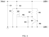
- Figure 3 shows this alternative embodiment.
- the buffer adjustment circuit further comprises an impedance R1 in series with the second capacitor C2 to limit the charging of the second capacitor C2, and the impedance R1 is in parallel with the switch M1.
- the buffer adjustment circuit is adapted to connect the first capacitor C1 and a series connection of the second capacitor C2 and the impedance R1 across the output in the start-up phase, by opening the switch M1 and connect the first capacitor C1 and the second capacitor C2 across the output while bypassing the impedance R1 in the normal operation phase, by closing the switch M1.
- the buffer adjustment circuit further comprises a bias circuit R7, R2 connected to a control terminal of the switch M1 and adapted to apply a bias voltage to the control terminal to close the switch M1, and a voltage detection circuit including resistor R3, resistor R8 and switch Q1 connected to the second capacitor C2, adapted to detect a signal indicative of the voltage across the impedance R1.
- the voltage detection circuit R3, R8, Q1 enables the bias voltage when the voltage across the impedance R1 is below a threshold. This occurs for example when the charging current for the second capacitor C2, also flowing through the impedance R1, is too low, indicating that the second capacitor is charged enough. This allows the switch M1 to close and enter the normal operation mode.
- the voltage detection circuit R3, R8, Q1 disables the bias voltage when the voltage across the impedance R1 is above the threshold. This means that the current through the second capacitor C2 and the impedance R1 is high, indicating that the second capacitor C2 is still charging, and that therefore the switch M1 needs to remain open.
- the LED driving circuit circuitry includes the first capacitor C1 and the second capacitor C2, and M1, R2, D3, Q1, R7, R3, R8 and R1.
- the MOSFET M1 is open and the transistor Q1 is also open since there is no voltage on both capacitors.
- the start-up phase begins once the power supply starts to output the LED driving current at the Vbus terminal, which will charge the output capacitors C1 and C2.
- R1 can be a fixed resistor (providing a fixed slow charging rate) or even a PTC resistor (providing a slower and slower charging rate as the PTC resistor becomes hot due to current flowing through it).
- the LED starts to give light, though temporarily not giving the nominal low ripple.
- the start-up phase ends.
- the capacitor C2 is charged to the voltage of the capacitor C1 as well as the LED forward voltage, and it will stop substantially charging (except for absorbing the ripple which current is relatively small).
- the charging current of capacitor C2 decreases, so decreases the voltage on the resistor R1.
- the transistor Q1 becomes open if the voltage VR1 on the resistor R1 is ⁇ 0.7*(R3+R6)/R6.
- the MOSFET M1 will be closed via a bias voltage from the Vbus, provided by the bias circuit R4 connected to the Vbus, and optionally via R2. So the capacitor C2 is directly connected to the Vbus without the extra impedance R1. It had better be that to select proper values of those components and make the capacitor C2 is almost at the same level as the capacitor C1 when the MOSFET M1 is closed, to avoid a large current sinking by the capacitor C2, thereby avoiding a dip in the LED driving current to the LED and avoiding light output flicker.
- the two capacitors C1 and C2 are in parallel afterwards, and provide a large capacitance to absorb the ripple in the LED driving current, the nominal light output ripple has been provided, and the normal operation phase starts.
- the Zener diode D3 at the gate of the MOSFET M1 is to protect the gate of the MOSFET M1 from a too high voltage.
- the Zener diode D3 can be replaced by a resistor.
- An advantage of the second embodiment is that the voltage detection circuit connects to the second capacitor, not to the LED directly, so it saves a wire to the LED board if the LED driving circuit is placed is a different board from the LED board, such as that the LED driving circuit is put in a standalone driver separate from the LED board.
- the capacitance of the capacitor C1 could be 330 ⁇ F and the capacitance of the capacitor C2 could be 660 ⁇ F.
- the resistances of R1, R2, R3, R4 and R6 could be 150Ohm, 22Ohm, 100K Ohm, 1000K Ohm and 100K Ohm respectively. Those values are all by way of example.
- the above LED driving circuit can be a part of a standalone LED powering circuit such as an electronic power driver for LED.
- the LED powering circuit comprises a power supply adapted to connect to a power source, such as AC mains and output a LED driving current, and the LED driving circuit as discussed above.
- the above LED powering circuit and a LED to be driven by the LED powering circuit can be combined together to form a standalone LED lighting device.
- the LED lighting device could be as small as a bulb, and as big as a luminaire.
- the buffer circuit can also be implemented in an inductive manner, since inductance is also capable of buffering the ripple in the LED driving current. More specifically, in the start-up phase the buffer circuit is adjusted by the buffer adjustment circuit with a smaller inductance to fast provide the driving current to the LED; and in the normal operation phase the buffer circuit adjusted by the buffer adjustment circuit with a larger inductance to buffer the ripple. Therefore, the way to dynamically change the inductance is similar as the above-mentioned way to dynamically change the capacitance, in terms of providing a fast start up in start-up phase and low ripple in normal operation phase are similar. Given description had described the invention mainly by taking capacitance buffering as example, those skilled in the art would implement the invention by inductive buffering and the application will not give detailed descriptions.
Landscapes
- Physics & Mathematics (AREA)
- Electromagnetism (AREA)
- Circuit Arrangement For Electric Light Sources In General (AREA)
- Led Devices (AREA)
Description
- This invention relates to a LED driving circuit. In particular it relates to a LED driving circuit with both advantages of low flicker in normal operation and fast start-up.
- With the continuous update of the technical requirements of LED lighting products, in the new Single Lighting Regulation (SLR) standards released in Europe, there are clear requirements for the Stroboscopic Visibility Measure (SVM) to measure the light output ripple. It temporarily requires SVM<0.4, and the final version after consultation and revision may require SVM<0.9. This means the current to the LED should have much less ripple than now.
- Traditionally the LED driving circuit has two stages, a first stage for power factor correction, PFC, whose output has large ripples, and a second stage to convert the output of the PFC stage into a smoother current so it can more or less solve the SVM requirement. However, a new trend is reducing the LED driving circuit into one stage or 1.5 stage, which has to implement PFC so its output to the LED still has considerable ripples. A further solution to make the ripple current acceptable is to increase significantly the capacitance of the output capacitor to smoothen the ripple. Such an output capacitor could be as large as hundreds of µF or even a thousand µF.
- However, another problem rises with the large output capacitor. The larger the output capacitor, the longer the time it takes to charge the output capacitor to a voltage that is sufficient to turn on the LED. According to EU requirements, the start-up time of LED lighting products needs to be less than 0.5s. If the LED lighting circuit is working in a dimming mode, and the power supply's output current is less than the maximum value, it takes quite a longer time to charge the large output capacitor before the LED starts to emit light, and this may not fulfill above requirement of the start-up time.
-
US2020205265A1 discloses providing a larger capacitance when the input voltage is 220V to 240V VAC and providing a smaller capacitance when the input volage is 100V to 120V VAC to meet requirement on harmonics. -
WO2012059853A1 discloses a valley fill technology wherein a capacitor is switched in to be charged by the input voltage at the moment the input voltage is sufficient to drive the LED via a power converter, and the capacitor is discharged to power the LED when the input voltage drops thereby no energy can be drawn from the input voltage. - The embodiments of the invention aim to provide both low flicker and fast start-up. The basic idea of the embodiments of the invention is dynamically changing the buffer capability of the buffer circuit of the LED driving circuit, providing a relatively low buffer capability in start-up so the output voltage can be fast built up to turn on the LED; and then increasing the buffer capability in normal operation after the start up so as to smooth the ripple. Therefore, the start-up time is shortened and the flicker in normal operation is reduced.
- According to a first aspect of the invention, a LED driving circuit is provided, which comprises: an input to receive a LED driving current, a buffer circuit adapted to buffer said LED driving current, and an output to be connected to an LED and adapted to output the LED driving current, after buffered, to the LED, characterized in that the LED driving circuit further comprises a buffer adjustment circuit adapted to adjust the buffer capability of the buffer circuit at a first level, in a start-up phase of the LED driving circuit when the LED driving circuit starts to receive said LED driving current, and adjust the buffer capability of the buffer circuit at a second level larger than the first level in a normal operation phase later than the start-up phase.
- According to this aspect, since in the start-up phase the buffer capability is not so high, the buffer circuit builds up to a sufficient electrical level to turn on the LED, namely starting-up the LED quickly; after the start-up, the buffer capability is increased so as to absorb the ripple in the LED driving current and to meet the requirement of low flicker. This achieves a balance of fast start up and low flicker in normal operation for LED lighting.
- In a detailed embodiment, the buffer circuit comprises at least one capacitor, and the buffer adjustment circuit is adapted to adjust an effective capacitance of the buffer circuit.
- In this embodiment, by dynamically adjusting the effective capacitance, the time for the buffer circuit to build a voltage to turn on the LED is shortened, and its buffer capability is then increased to meet both requirement of fast start-up and low flicker.
- In the invention the start-up phase is a phase in which a voltage on the output and the at least one capacitor is being built and insufficient to turn on the LED, and the normal operation phase is a phase in which the voltage on the output and the at least one capacitor has been built up sufficient and turned on the LED, and the nominal light output ripple has been provided.
- Thus the start-up phase is building the output voltage to reach the LED forward voltage before the LED can be turned on; and the normal operation phase is the phase where the output voltage has reached the LED forward voltage and the LED is turned on, and the nominal light output ripple has been provided.
- In a detailed embodiment, the buffer circuit comprises a first capacitor and a second capacitor connected in parallel across the output, and the buffer adjustment circuit comprises a switch in series with the second capacitor across the output.
- This embodiment gives a relatively simple circuit to provide an adjustable effective capacitance providing a first capacitor as a base capacitance and controlling how much is the involvement of a second capacitor via a switch.
- In a further embodiment, the buffer adjustment circuit is adapted to connect the first capacitor across the output and disconnect the second capacitor from the output in the start-up phase, by opening the switch; and connect both of the first capacitor and the second capacitor across the output in the normal operation phase, by closing the switch.
- This embodiment switches out the second capacitor in the start-up phase and let the first capacitor to build the LED forward voltage, so the start-up time is short; after start-up, this embodiment switches in the second capacitor to absorb ripple and reduce ripple.
- In a further embodiment, in order to avoid a sudden switching in of the second capacitor and causing a large current sinking effect, the buffer adjustment circuit is adapted to make the switch operate in a current limiting mode to limit the current flowing through the second capacitor and the switch during a transition of connecting the second capacitor across the output, and make the switch operate in fully conduction mode in the normal operation mode.
- This embodiment limits the current sinking by the second capacitor, and avoids a sudden drop of current to the LED and avoid dip/flicker in light output.
- In an alternative embodiment, the buffer adjustment circuit further comprises an impedance in series with the second capacitor and in parallel with the switch.
- Instead of switching the second capacitor, this alternative embodiment switches an extra impedance in series with the second capacitor so as to change a time response of the second capacitor.
- Preferably, the buffer adjustment circuit is adapted to connect the first capacitor and a series connection of the second capacitor and the impedance across the output in the start-up phase, by opening the switch; and connect the first capacitor and the second capacitor across the output while bypassing the impedance in the normal operation phase, by closing the switch.
- In this preferred embodiment, the second capacitor is also charged, though slowly, in the start-up phase, thus the second capacitor can smoothly transition into the normal operation phase without sinking much current from the first capacitor and the LED. This avoids a high visible light drop.
- More specifically, the buffer adjustment circuit further comprises a bias circuit connected to a control terminal of the switch and adapted to apply a bias voltage to the control terminal to close the switch; a voltage detection circuit connected to the second capacitor, adapted to detect a signal indicative of the voltage on the second capacitor, and to disable the bias voltage when the voltage on the second capacitor is below a threshold; to enable the bias voltage when the voltage on the second capacitor is above the threshold.
- This embodiment provides a detection on the charging of the second capacitor: if it is detected that the second capacitor is already charged sufficiently, the impedance can be bypassed, and the second capacitor can be used more efficiently without influencing the light output.
- In a second aspect of the invention, a LED powering circuit is provided and comprising a power supply adapted to connect to a power source and converter an energy of the power source into the LED driving current, and the LED driving circuit of the first aspect.
- This aspect provides a power electronic circuit as a whole, including the power supply function and the buffer function, with fast start-up and low flicker advantage. The LED powering circuit could be a standalone LED driver.
- In a third aspect of the invention, a LED lighting device is provided, comprising LED and the LED powering circuit according to the second aspect.
- This aspect provides a lighting device as a whole, including the LED and the LED powering circuit. The LED lighting device could be either a bulb, or a luminaire.
- These and other aspects of the invention will be apparent from and elucidated with reference to the embodiment(s) described hereinafter.
- For a better understanding of the invention, and to show more clearly how it may be carried into effect, reference will now be made, by way of example only, to the accompanying drawings, in which:
-
Fig. 1 shows a LED driving circuit according to one embodiment of the invention; -
Fig. 2 shows an improvement of the embodiment shown infig. 1 ; and -
Fig. 3 shows another LED driving circuit according to another embodiment of the invention. - The invention will be described with reference to the Figures.
- It should be understood that the detailed description and specific examples, while indicating exemplary embodiments of the apparatus, systems and methods, are intended for purposes of illustration only and are not intended to limit the scope of the invention. These and other features, aspects, and advantages of the apparatus, systems and methods of the present invention will become better understood from the following description, appended claims, and accompanying drawings. It should be understood that the Figures are merely schematic and are not drawn to scale. It should also be understood that the same reference numerals are used throughout the Figures to indicate the same or similar parts.
- As shown in
figures 1 ,2 and3 , embodiments of the invention propose a LED driving circuit comprising: - an input Vbus to receive a LED driving current,
- a buffer circuit C1 and C2 adapted to buffer said LED driving current, and
- an output LED+ and LED- to be connected to LED and adapted to output the LED driving current, after buffered, to the LED,
characterized in that the LED driving circuit further comprises - a buffer adjustment circuit including M1, among other components, adapted to
- adjust the buffer capability of the buffer circuit at a first level, in a start-up phase of the LED driving circuit when the LED driving circuit starts to receive said LED driving current, and
- adjust the buffer capability of the buffer circuit at a second level larger than the first level in a normal operation phase later than the start-up phase.
- In a preferred embodiment, the buffer circuit is capacitive, and comprises at least one capacitor, and the buffer adjustment circuit is adapted to adjust an effective capacitance of the buffer circuit. Capacitive buffering is a widely used implementation in LED driving.
- The start-up phase is a phase in which a voltage on the output and the at least one capacitor is being built up and insufficient to turn on the LED, and the normal operation phase is a phase in which the voltage on the output and the at least one capacitor has been built up sufficiently and turned on the LED and the nominal light output ripple has been provided. There could be a transition between the start-up phase and the normal operation phase, during which the capacitance is being adjusted. Below description will describe this.
- In order to implement an adjustable capacitance, an easy topology is to provide two capacitors wherein one capacitor is associated with a switch to control the charging of that capacitor. More specifically, as shown in
figures 1 and2 , the buffer circuit comprises a first capacitor C1 and a second capacitor C2 and the buffer adjustment circuit. The buffer adjustment circuit comprises a switch M1 in series with the second capacitor C2 while the series connection of the second capacitor C2 and the switch M1 is across the output LED+ and LED-. Preferably, the series connection of the second capacitor C2 and the buffer adjustment circuit is placed in parallel with the first capacitor C1. - In the embodiment shown in
figure 1 , the LED driving current, from a power supply, flows in at the Vbus terminal. In order to change the effective capacitance of the two capacitors C1 and C2, the buffer adjustment circuit is adapted to allow the first capacitor C1 being connected across the output and disconnect the second capacitor C2 from the output or input in the start-up phase, by opening the switch M1 and connect both of the first capacitor C1 and the second capacitor C2 across the output in the normal operation phase, by closing the switch M1. The trigger of the switch M1 can originate from an established LED forward voltage, meaning that when the LED has been turned on, a current flows through the LED, the switch M1 closes and connects the second capacitor C2 to the Vbus terminal. - More specifically, the GS terminal may be tapped from a segment of LEDs whose forward voltage is preferably 5V or 10V. When the LED is on, this GS voltage is applied to the gate of the MOSFET M1 and closes the MOSFET M1. An optional resistor R0 is connected between the gate and source of the MOSFET M1 to protect the gate of the MOSFET M1 from an overvoltage. The resistance of the resistor R0 could be 47K Ohm.
- Since the second capacitor may be empty when the switch M1 is to switch on, the second capacitor would intend to sink a large current from the LED driving current or even from the first capacitor C1, which may cause a dip in the LED driving current to the LED. In order to have a smooth connection of the second capacitor C2, in the improved embodiment shown in
figure 2 , the buffer adjustment circuit is adapted to make the switch M1 operate in a current limiting mode to limit the current flowing through the second capacitor C2 and the switch M1 during a transition of connecting the second capacitor C2 across the output. The limited current is preferably at an amplitude that it would not cause unacceptable light output drop. The real value can be designed by those skilled in the art according to practical needs. - In the embodiment in
figure 2 , the Vcc is used to provide a power supply to an op-amp U1 and retrieve a reference signal, via a voltage divider formed by the resistors R5 and R6, from the Vcc. The reference signal is connected to the positive input of the op-amp U1A. A small sensing resistor R4 is connected in series with the capacitor C2 to sense the charging current of C2, and the current is feedback to the negative input of the op-amp U1. In order to reduce power losses, the resistance of the sensing resistor R4 could be up to 10 Ohm. When the LED is on and the Vcc voltage is available, the op-amp is turned on and compares the sensed charging current and the reference, and outputs a signal to drive the MOSFET M1 in such a way that the charging current conforms to the reference. This a common way of a current source in controlling a current. An unshown detection circuit may detect that the second capacitor C2 is charged to substantially the LED forward voltage, or almost equal to the voltage on the first capacitor C1, and injects a high voltage gate driving signal GD to the gate of the MOSFET M1 to override the signal from the op-amp. The high voltage gate driving signal GD makes the switch M1 enter a fully conduction mode, not limiting the current flowing through the second capacitor C2 anymore. Then the two capacitors C1 and C2 are in substantially pure parallel connection with a large capacitance that is the sum of both capacitances. - The capacitance of C1 is 1µF and the capacitance of C2 is 150µF, as shown in the
figures 1 and2 , but this is only an example. Those skilled in the art are knowledgeable to select proper values according to the real requirement in start-up time and light output ripple. - In the above embodiment, the second capacitor is totally cut off from the output and not charged at all in the start-up phase. In an alternative embodiment, the LED driving circuit can allow the second capacitor also being charged but use a large impedance to limit its charging in the start-up phase, so it is still mainly the first capacitor C1 to be charged by the power supply and to build the LED forward voltage quickly.
Figure 3 shows this alternative embodiment. The buffer adjustment circuit further comprises an impedance R1 in series with the second capacitor C2 to limit the charging of the second capacitor C2, and the impedance R1 is in parallel with the switch M1. - The buffer adjustment circuit is adapted to connect the first capacitor C1 and a series connection of the second capacitor C2 and the impedance R1 across the output in the start-up phase, by opening the switch M1 and connect the first capacitor C1 and the second capacitor C2 across the output while bypassing the impedance R1 in the normal operation phase, by closing the switch M1. The buffer adjustment circuit further comprises a bias circuit R7, R2 connected to a control terminal of the switch M1 and adapted to apply a bias voltage to the control terminal to close the switch M1, and a voltage detection circuit including resistor R3, resistor R8 and switch Q1 connected to the second capacitor C2, adapted to detect a signal indicative of the voltage across the impedance R1. The voltage detection circuit R3, R8, Q1 enables the bias voltage when the voltage across the impedance R1 is below a threshold. This occurs for example when the charging current for the second capacitor C2, also flowing through the impedance R1, is too low, indicating that the second capacitor is charged enough. This allows the switch M1 to close and enter the normal operation mode. The voltage detection circuit R3, R8, Q1 disables the bias voltage when the voltage across the impedance R1 is above the threshold. This means that the current through the second capacitor C2 and the impedance R1 is high, indicating that the second capacitor C2 is still charging, and that therefore the switch M1 needs to remain open.
- More specifically, referring to
figure 3 , the LED driving circuit circuitry includes the first capacitor C1 and the second capacitor C2, and M1, R2, D3, Q1, R7, R3, R8 and R1. Before the start-up phase, there is no electrical charge in this circuit. Both capacitors C1 and C2 are fully empty and their voltages are 0V, the MOSFET M1 is open and the transistor Q1 is also open since there is no voltage on both capacitors. The start-up phase begins once the power supply starts to output the LED driving current at the Vbus terminal, which will charge the output capacitors C1 and C2. C1 has no problem of being charged at a normal rate, but the capacitor C2 will be charged with a smaller current/low rate due to that the impedance R1, implemented by a resistor, is in series with the capacitor C2. R1 can be a fixed resistor (providing a fixed slow charging rate) or even a PTC resistor (providing a slower and slower charging rate as the PTC resistor becomes hot due to current flowing through it). When the capacitor C2 is still being charged, there is a charging current also flowing through the resistor R1, thus across the resistor R1 there will be a voltage VR1>0.7*(R3+R6)/R6, wherein the 0.7V is the close threshold of the transistor Q1, so that transistor Q1 is close via the voltage divider R3 and R6, the transistor Q1 shunts the gate of the MOSFET M1 to ground, and the MOSFET M1 remains open. The power supply is loaded mainly with the capacitor C1, and very slightly with the series connection of the capacitor C2 and the resistor R1. The LED driving current would go to the capacitor C1 by a large portion to charge it. Once the voltage on the capacitor C1 reaches the LED forward voltage, the LED starts to give light, though temporarily not giving the nominal low ripple. The start-up phase ends. In a transition phase between the start-up phase to the normal operation phase, the capacitor C2 is charged to the voltage of the capacitor C1 as well as the LED forward voltage, and it will stop substantially charging (except for absorbing the ripple which current is relatively small). The charging current of capacitor C2 decreases, so decreases the voltage on the resistor R1. The transistor Q1 becomes open if the voltage VR1 on the resistor R1 is <0.7*(R3+R6)/R6. Once the transistor Q1 is open, the MOSFET M1 will be closed via a bias voltage from the Vbus, provided by the bias circuit R4 connected to the Vbus, and optionally via R2. So the capacitor C2 is directly connected to the Vbus without the extra impedance R1. It had better be that to select proper values of those components and make the capacitor C2 is almost at the same level as the capacitor C1 when the MOSFET M1 is closed, to avoid a large current sinking by the capacitor C2, thereby avoiding a dip in the LED driving current to the LED and avoiding light output flicker. The two capacitors C1 and C2 are in parallel afterwards, and provide a large capacitance to absorb the ripple in the LED driving current, the nominal light output ripple has been provided, and the normal operation phase starts. After the MOSFET M1 is close, VR1=0 and the transistor Q1 remains open afterward. In this way the MOSFET M1 is always close and latched, as long as the power supply is still powered on and providing the LED driving current. The effective capacitance/buffer capability of the circuitry in the normal operation phase is higher than that in the start-up phase. The Zener diode D3 at the gate of the MOSFET M1 is to protect the gate of the MOSFET M1 from a too high voltage. The Zener diode D3 can be replaced by a resistor. - An advantage of the second embodiment is that the voltage detection circuit connects to the second capacitor, not to the LED directly, so it saves a wire to the LED board if the LED driving circuit is placed is a different board from the LED board, such as that the LED driving circuit is put in a standalone driver separate from the LED board.
- The capacitance of the capacitor C1 could be 330µF and the capacitance of the capacitor C2 could be 660µF. The resistances of R1, R2, R3, R4 and R6 could be 150Ohm, 22Ohm, 100K Ohm, 1000K Ohm and 100K Ohm respectively. Those values are all by way of example.
- The above LED driving circuit can be a part of a standalone LED powering circuit such as an electronic power driver for LED. The LED powering circuit comprises a power supply adapted to connect to a power source, such as AC mains and output a LED driving current, and the LED driving circuit as discussed above.
- The above LED powering circuit and a LED to be driven by the LED powering circuit can be combined together to form a standalone LED lighting device. The LED lighting device could be as small as a bulb, and as big as a luminaire.
- The above embodiment uses capacitors to describe the buffering circuit, and the applicant submits that this is not the only choice. Alternatively, the buffer circuit can also be implemented in an inductive manner, since inductance is also capable of buffering the ripple in the LED driving current. More specifically, in the start-up phase the buffer circuit is adjusted by the buffer adjustment circuit with a smaller inductance to fast provide the driving current to the LED; and in the normal operation phase the buffer circuit adjusted by the buffer adjustment circuit with a larger inductance to buffer the ripple. Therefore, the way to dynamically change the inductance is similar as the above-mentioned way to dynamically change the capacitance, in terms of providing a fast start up in start-up phase and low ripple in normal operation phase are similar. Given description had described the invention mainly by taking capacitance buffering as example, those skilled in the art would implement the invention by inductive buffering and the application will not give detailed descriptions.
- Variations to the disclosed embodiments can be understood and effected by those skilled in the art in practicing the claimed invention, from a study of the drawings, the disclosure and the appended claims. In the claims, the word "comprising" does not exclude other elements or steps, and the indefinite article "a" or "an" does not exclude a plurality.
- The mere fact that certain measures are recited in mutually different dependent claims does not indicate that a combination of these measures cannot be used to advantage.
- If the term "adapted to" is used in the claims or description, it is noted the term "adapted to" is intended to be equivalent to the term "configured to".
- Any reference signs in the claims should not be construed as limiting the scope.
Claims (9)
- A LED driving circuit comprising:- an input (Vbus) to receive a LED driving current,- a buffer circuit adapted to buffer said LED driving current, and- an output (LED+, LED-) to be connected to a LED and adapted to output the LED driving current to the LED,- a buffer adjustment circuit adapted to:adjust the buffer capability of the buffer circuit at a first level, in a start-up phase of the LED driving circuit when the LED driving circuit starts to receive said LED driving current, andadjust the buffer capability of the buffer circuit at a second level larger than the first level in a normal operation phase later than the start-up phase,whereinthe buffer circuit comprises at least one capacitor, and the buffer adjustment circuit is adapted to adjust an effective capacitance of the buffer circuit;characterised in that the start-up phase is a phase in which a voltage on the output (LED+, LED-) and the at least one capacitor is being built and insufficient to turn on the LED, and the normal operation phase is a phase in which the voltage on the output (LED+, LED-) and the at least one capacitor has been built sufficient and turned on the LED, and the nominal light output ripple has been provided.
- The LED driving circuit according to claim 1, wherein the buffer circuit comprisesa first capacitor (C1) and a second capacitor (C2) connected in parallel across the output (LED+, LED-), andthe buffer adjustment circuit comprises a switch (M1) in series with the second capacitor (C2) across the output (LED+, LED-).
- The LED driving circuit according to claim 2, wherein the buffer adjustment circuit is adapted to:connect the first capacitor (C1) across the output (LED+, LED-) and disconnect the second capacitor (C2) from the output in the start-up phase, by opening the switch (M1); andconnect both of the first capacitor (C1) and the second capacitor (C2) across the output (LED+, LED-) in the normal operation phase, by closing the switch (M1).
- The LED driving circuit according to claim 3, wherein the buffer adjustment circuit is adapted tomake the switch (M1) operate in a current limiting mode to limit the current flowing through the second capacitor (C2) and the switch (M1) during a transition of connecting the second capacitor (C2) across the output (LED+, LED-); andmake the switch (M1) operate in fully conduction mode in the normal operation mode.
- The LED driving circuit according to claim 4, wherein the buffer adjustment circuit further comprises an impedance (R1) in series with the second capacitor (C2) and in parallel with the switch (M1).
- The LED driving circuit according to claim 5, wherein the buffer adjustment circuit is adapted toconnect the first capacitor (C1) and a series connection of the second capacitor (C2) and the impedance (R1) across the output (LED+, LED-) in the start-up phase, by opening the switch (M1); andconnect the first capacitor (C1) and the second capacitor (C2) across the output (LED+, LED-) while bypassing the impedance (R1) in the normal operation phase, by closing the switch (M1).
- The LED driving circuit according to claim 5, wherein the buffer adjustment circuit further comprisesa bias circuit (R4) connected to a control terminal of the switch (M1) and adapted to apply a bias voltage to the control terminal to close the switch (M1); anda voltage detection circuit (R3, R6, Q1) connected to the second capacitor (C2), adapted to detect a signal indicative of the voltage on the second capacitor (C2), andto disable the bias voltage when the voltage on the second capacitor (C2) is below a threshold; andto enable the bias voltage when the voltage on the second capacitor (C2) is above the threshold.
- A LED powering circuit comprisinga power supply adapted to connect to a power source, and convert an energy of the power source into the LED driving current; andthe LED driving circuit according to any one of claims 1 to 7.
- A LED lighting device, comprising LED; and
the LED powering circuit according to claim 8.
Applications Claiming Priority (3)
| Application Number | Priority Date | Filing Date | Title |
|---|---|---|---|
| CN2021079758 | 2021-03-09 | ||
| EP21185094 | 2021-07-12 | ||
| PCT/EP2022/055682 WO2022189326A1 (en) | 2021-03-09 | 2022-03-07 | Led driving circuit, led powering circuit, and led lighting device |
Publications (2)
| Publication Number | Publication Date |
|---|---|
| EP4305928A1 EP4305928A1 (en) | 2024-01-17 |
| EP4305928B1 true EP4305928B1 (en) | 2025-05-21 |
Family
ID=80953268
Family Applications (1)
| Application Number | Title | Priority Date | Filing Date |
|---|---|---|---|
| EP22713390.7A Active EP4305928B1 (en) | 2021-03-09 | 2022-03-07 | Led driving circuit, led powering circuit, and led lighting device |
Country Status (6)
| Country | Link |
|---|---|
| US (1) | US12526894B2 (en) |
| EP (1) | EP4305928B1 (en) |
| JP (1) | JP2024511568A (en) |
| CN (1) | CN116998221A (en) |
| ES (1) | ES3034406T3 (en) |
| WO (1) | WO2022189326A1 (en) |
Families Citing this family (1)
| Publication number | Priority date | Publication date | Assignee | Title |
|---|---|---|---|---|
| EP4483675B1 (en) * | 2022-02-24 | 2025-10-01 | Signify Holding B.V. | Dual tapped l2 supply configuration for tled lamps |
Family Cites Families (13)
| Publication number | Priority date | Publication date | Assignee | Title |
|---|---|---|---|---|
| JP2009519787A (en) * | 2005-12-19 | 2009-05-21 | テックミン ピーティーワイ リミテッド | Management and display of medical devices |
| JP5042879B2 (en) | 2007-09-25 | 2012-10-03 | パナソニック株式会社 | Switching power supply |
| WO2012059853A1 (en) | 2010-11-03 | 2012-05-10 | Koninklijke Philips Electronics N.V. | Driver device and driving method for driving a load, in particular an led unit |
| JP2012147521A (en) | 2011-01-07 | 2012-08-02 | Seiko Epson Corp | Power circuit, electronic apparatus, and control method |
| US8749163B2 (en) | 2011-09-22 | 2014-06-10 | Astec International Limited | LED driver circuits |
| DE102011088407A1 (en) * | 2011-12-13 | 2013-06-13 | Osram Gmbh | Circuit arrangement and method for operating an LED chain and lighting device with such a circuit arrangement and an LED chain |
| JP2013128372A (en) | 2011-12-19 | 2013-06-27 | Hitachi Cable Ltd | Dc power supply circuit |
| US10136480B2 (en) | 2012-03-16 | 2018-11-20 | Philips Lighting Holding B.V. | Circuit arrangement |
| US9215765B1 (en) | 2012-10-26 | 2015-12-15 | Philips International, B.V. | Systems and methods for low-power lamp compatibility with an electronic transformer |
| JP6883153B2 (en) * | 2018-03-29 | 2021-06-09 | シグニファイ ホールディング ビー ヴィSignify Holding B.V. | Lighting unit and driving method |
| JP6892410B2 (en) | 2018-04-13 | 2021-06-23 | きらぼしテック株式会社 | Payroll prepayment system, payroll prepayment device, program, and payroll prepayment method |
| CN109862655A (en) | 2018-10-17 | 2019-06-07 | 矽力杰半导体技术(杭州)有限公司 | Integrated circuit, dimmable LED driving circuit and driving method thereof |
| CN111343768A (en) * | 2018-12-19 | 2020-06-26 | 台达电子企业管理(上海)有限公司 | LED driving device and LED driving method |
-
2022
- 2022-03-07 JP JP2023555181A patent/JP2024511568A/en active Pending
- 2022-03-07 US US18/279,278 patent/US12526894B2/en active Active
- 2022-03-07 ES ES22713390T patent/ES3034406T3/en active Active
- 2022-03-07 EP EP22713390.7A patent/EP4305928B1/en active Active
- 2022-03-07 WO PCT/EP2022/055682 patent/WO2022189326A1/en not_active Ceased
- 2022-03-07 CN CN202280020415.8A patent/CN116998221A/en active Pending
Also Published As
| Publication number | Publication date |
|---|---|
| US20240121871A1 (en) | 2024-04-11 |
| US12526894B2 (en) | 2026-01-13 |
| CN116998221A (en) | 2023-11-03 |
| EP4305928A1 (en) | 2024-01-17 |
| JP2024511568A (en) | 2024-03-14 |
| ES3034406T3 (en) | 2025-08-18 |
| WO2022189326A1 (en) | 2022-09-15 |
Similar Documents
| Publication | Publication Date | Title |
|---|---|---|
| US8829812B2 (en) | Dimmable lighting system | |
| EP2630842B1 (en) | Led retrofit lamp | |
| JP6921138B2 (en) | Dimmable lighting system | |
| KR101682722B1 (en) | Inrush current limiter for an led driver | |
| KR101997888B1 (en) | Adaptive circuit | |
| US9060396B2 (en) | Mechanisms for anti-flickering | |
| US9769890B1 (en) | Circuit and method for eliminating power-off flash for LED drivers | |
| CN103999548B (en) | Circuit arrangement and method for operating an LED chain with alternating voltage | |
| US20160262234A1 (en) | Circuit assembly for operating at least a first and a second cascade of leds | |
| EP2709252B1 (en) | LED lighting device | |
| US20140361691A1 (en) | Lighting system | |
| US12526894B2 (en) | LED driving circuit, LED powering circuit, and LED lighting device | |
| JP2019536405A (en) | AC / DC converter with power factor correction | |
| CN106489303B (en) | Apparatus and method for phase-cut power control | |
| CN101820706B (en) | Device and method for dimming light sources | |
| CN107820348B (en) | Linear full-voltage variable-frequency constant-current circuit and LED lamp with same | |
| CN110035579B (en) | High-power-factor non-stroboscopic linear control method compatible with silicon controlled rectifier dimmer and control device used in method | |
| US20140021872A1 (en) | Circuit for controlling a lighting unit with light-emitting diodes | |
| EP3874910A1 (en) | Led lighting driver and drive method | |
| CN2842869Y (en) | Constant voltage-current charging circuit | |
| KR102130176B1 (en) | Power supply circuit for alteration of flicker frequency of light emitting diode | |
| EP3322081A1 (en) | Pre-regulator for a dimmer | |
| JP2025524307A (en) | LED lighting circuit and LED lighting fixture having LED lighting circuit | |
| WO2020083876A1 (en) | Electronic controller apparatus and control method | |
| JPS5936506B2 (en) | AC power control circuit |
Legal Events
| Date | Code | Title | Description |
|---|---|---|---|
| STAA | Information on the status of an ep patent application or granted ep patent |
Free format text: STATUS: UNKNOWN |
|
| STAA | Information on the status of an ep patent application or granted ep patent |
Free format text: STATUS: THE INTERNATIONAL PUBLICATION HAS BEEN MADE |
|
| PUAI | Public reference made under article 153(3) epc to a published international application that has entered the european phase |
Free format text: ORIGINAL CODE: 0009012 |
|
| STAA | Information on the status of an ep patent application or granted ep patent |
Free format text: STATUS: REQUEST FOR EXAMINATION WAS MADE |
|
| 17P | Request for examination filed |
Effective date: 20231009 |
|
| AK | Designated contracting states |
Kind code of ref document: A1 Designated state(s): AL AT BE BG CH CY CZ DE DK EE ES FI FR GB GR HR HU IE IS IT LI LT LU LV MC MK MT NL NO PL PT RO RS SE SI SK SM TR |
|
| DAV | Request for validation of the european patent (deleted) | ||
| DAX | Request for extension of the european patent (deleted) | ||
| GRAP | Despatch of communication of intention to grant a patent |
Free format text: ORIGINAL CODE: EPIDOSNIGR1 |
|
| STAA | Information on the status of an ep patent application or granted ep patent |
Free format text: STATUS: GRANT OF PATENT IS INTENDED |
|
| INTG | Intention to grant announced |
Effective date: 20241213 |
|
| GRAS | Grant fee paid |
Free format text: ORIGINAL CODE: EPIDOSNIGR3 |
|
| GRAA | (expected) grant |
Free format text: ORIGINAL CODE: 0009210 |
|
| STAA | Information on the status of an ep patent application or granted ep patent |
Free format text: STATUS: THE PATENT HAS BEEN GRANTED |
|
| AK | Designated contracting states |
Kind code of ref document: B1 Designated state(s): AL AT BE BG CH CY CZ DE DK EE ES FI FR GB GR HR HU IE IS IT LI LT LU LV MC MK MT NL NO PL PT RO RS SE SI SK SM TR |
|
| P01 | Opt-out of the competence of the unified patent court (upc) registered |
Free format text: CASE NUMBER: APP_17598/2025 Effective date: 20250410 |
|
| REG | Reference to a national code |
Ref country code: GB Ref legal event code: FG4D |
|
| REG | Reference to a national code |
Ref country code: CH Ref legal event code: EP |
|
| REG | Reference to a national code |
Ref country code: DE Ref legal event code: R096 Ref document number: 602022014943 Country of ref document: DE |
|
| REG | Reference to a national code |
Ref country code: IE Ref legal event code: FG4D |
|
| REG | Reference to a national code |
Ref country code: SE Ref legal event code: TRGR |
|
| REG | Reference to a national code |
Ref country code: ES Ref legal event code: FG2A Ref document number: 3034406 Country of ref document: ES Kind code of ref document: T3 Effective date: 20250818 |
|
| REG | Reference to a national code |
Ref country code: NL Ref legal event code: MP Effective date: 20250521 |
|
| PG25 | Lapsed in a contracting state [announced via postgrant information from national office to epo] |
Ref country code: FI Free format text: LAPSE BECAUSE OF FAILURE TO SUBMIT A TRANSLATION OF THE DESCRIPTION OR TO PAY THE FEE WITHIN THE PRESCRIBED TIME-LIMIT Effective date: 20250521 Ref country code: PT Free format text: LAPSE BECAUSE OF FAILURE TO SUBMIT A TRANSLATION OF THE DESCRIPTION OR TO PAY THE FEE WITHIN THE PRESCRIBED TIME-LIMIT Effective date: 20250922 |
|
| REG | Reference to a national code |
Ref country code: LT Ref legal event code: MG9D |
|
| PG25 | Lapsed in a contracting state [announced via postgrant information from national office to epo] |
Ref country code: NO Free format text: LAPSE BECAUSE OF FAILURE TO SUBMIT A TRANSLATION OF THE DESCRIPTION OR TO PAY THE FEE WITHIN THE PRESCRIBED TIME-LIMIT Effective date: 20250821 Ref country code: GR Free format text: LAPSE BECAUSE OF FAILURE TO SUBMIT A TRANSLATION OF THE DESCRIPTION OR TO PAY THE FEE WITHIN THE PRESCRIBED TIME-LIMIT Effective date: 20250822 |
|
| PG25 | Lapsed in a contracting state [announced via postgrant information from national office to epo] |
Ref country code: NL Free format text: LAPSE BECAUSE OF FAILURE TO SUBMIT A TRANSLATION OF THE DESCRIPTION OR TO PAY THE FEE WITHIN THE PRESCRIBED TIME-LIMIT Effective date: 20250521 Ref country code: PL Free format text: LAPSE BECAUSE OF FAILURE TO SUBMIT A TRANSLATION OF THE DESCRIPTION OR TO PAY THE FEE WITHIN THE PRESCRIBED TIME-LIMIT Effective date: 20250521 |
|
| PG25 | Lapsed in a contracting state [announced via postgrant information from national office to epo] |
Ref country code: BG Free format text: LAPSE BECAUSE OF FAILURE TO SUBMIT A TRANSLATION OF THE DESCRIPTION OR TO PAY THE FEE WITHIN THE PRESCRIBED TIME-LIMIT Effective date: 20250521 |
|
| PG25 | Lapsed in a contracting state [announced via postgrant information from national office to epo] |
Ref country code: HR Free format text: LAPSE BECAUSE OF FAILURE TO SUBMIT A TRANSLATION OF THE DESCRIPTION OR TO PAY THE FEE WITHIN THE PRESCRIBED TIME-LIMIT Effective date: 20250521 |
|
| PG25 | Lapsed in a contracting state [announced via postgrant information from national office to epo] |
Ref country code: RS Free format text: LAPSE BECAUSE OF FAILURE TO SUBMIT A TRANSLATION OF THE DESCRIPTION OR TO PAY THE FEE WITHIN THE PRESCRIBED TIME-LIMIT Effective date: 20250821 |
|
| PG25 | Lapsed in a contracting state [announced via postgrant information from national office to epo] |
Ref country code: IS Free format text: LAPSE BECAUSE OF FAILURE TO SUBMIT A TRANSLATION OF THE DESCRIPTION OR TO PAY THE FEE WITHIN THE PRESCRIBED TIME-LIMIT Effective date: 20250921 |
|
| PG25 | Lapsed in a contracting state [announced via postgrant information from national office to epo] |
Ref country code: LV Free format text: LAPSE BECAUSE OF FAILURE TO SUBMIT A TRANSLATION OF THE DESCRIPTION OR TO PAY THE FEE WITHIN THE PRESCRIBED TIME-LIMIT Effective date: 20250521 |
|
| REG | Reference to a national code |
Ref country code: AT Ref legal event code: MK05 Ref document number: 1798027 Country of ref document: AT Kind code of ref document: T Effective date: 20250521 |
|
| PG25 | Lapsed in a contracting state [announced via postgrant information from national office to epo] |
Ref country code: AT Free format text: LAPSE BECAUSE OF FAILURE TO SUBMIT A TRANSLATION OF THE DESCRIPTION OR TO PAY THE FEE WITHIN THE PRESCRIBED TIME-LIMIT Effective date: 20250521 Ref country code: SM Free format text: LAPSE BECAUSE OF FAILURE TO SUBMIT A TRANSLATION OF THE DESCRIPTION OR TO PAY THE FEE WITHIN THE PRESCRIBED TIME-LIMIT Effective date: 20250521 Ref country code: DK Free format text: LAPSE BECAUSE OF FAILURE TO SUBMIT A TRANSLATION OF THE DESCRIPTION OR TO PAY THE FEE WITHIN THE PRESCRIBED TIME-LIMIT Effective date: 20250521 |
|
| PG25 | Lapsed in a contracting state [announced via postgrant information from national office to epo] |
Ref country code: CZ Free format text: LAPSE BECAUSE OF FAILURE TO SUBMIT A TRANSLATION OF THE DESCRIPTION OR TO PAY THE FEE WITHIN THE PRESCRIBED TIME-LIMIT Effective date: 20250521 |
|
| PG25 | Lapsed in a contracting state [announced via postgrant information from national office to epo] |
Ref country code: EE Free format text: LAPSE BECAUSE OF FAILURE TO SUBMIT A TRANSLATION OF THE DESCRIPTION OR TO PAY THE FEE WITHIN THE PRESCRIBED TIME-LIMIT Effective date: 20250521 |
|
| PG25 | Lapsed in a contracting state [announced via postgrant information from national office to epo] |
Ref country code: SK Free format text: LAPSE BECAUSE OF FAILURE TO SUBMIT A TRANSLATION OF THE DESCRIPTION OR TO PAY THE FEE WITHIN THE PRESCRIBED TIME-LIMIT Effective date: 20250521 |
|
| REG | Reference to a national code |
Ref country code: DE Ref legal event code: R097 Ref document number: 602022014943 Country of ref document: DE |
|
| PLBE | No opposition filed within time limit |
Free format text: ORIGINAL CODE: 0009261 |
|
| STAA | Information on the status of an ep patent application or granted ep patent |
Free format text: STATUS: NO OPPOSITION FILED WITHIN TIME LIMIT |
|
| REG | Reference to a national code |
Ref country code: CH Ref legal event code: L10 Free format text: ST27 STATUS EVENT CODE: U-0-0-L10-L00 (AS PROVIDED BY THE NATIONAL OFFICE) Effective date: 20260402 |
|
| PGFP | Annual fee paid to national office [announced via postgrant information from national office to epo] |
Ref country code: SE Payment date: 20260323 Year of fee payment: 5 |
|
| PGFP | Annual fee paid to national office [announced via postgrant information from national office to epo] |
Ref country code: GB Payment date: 20260319 Year of fee payment: 5 |
|
| PGFP | Annual fee paid to national office [announced via postgrant information from national office to epo] |
Ref country code: IT Payment date: 20260320 Year of fee payment: 5 |
|
| PGFP | Annual fee paid to national office [announced via postgrant information from national office to epo] |
Ref country code: FR Payment date: 20260323 Year of fee payment: 5 |
|
| 26N | No opposition filed |
Effective date: 20260224 |