EP4303916A1 - Semiconductor module - Google Patents
Semiconductor module Download PDFInfo
- Publication number
- EP4303916A1 EP4303916A1 EP21929087.1A EP21929087A EP4303916A1 EP 4303916 A1 EP4303916 A1 EP 4303916A1 EP 21929087 A EP21929087 A EP 21929087A EP 4303916 A1 EP4303916 A1 EP 4303916A1
- Authority
- EP
- European Patent Office
- Prior art keywords
- support member
- resin mold
- outer terminals
- terminal
- terminals
- Prior art date
- Legal status (The legal status is an assumption and is not a legal conclusion. Google has not performed a legal analysis and makes no representation as to the accuracy of the status listed.)
- Granted
Links
Images




Classifications
-
- H—ELECTRICITY
- H02—GENERATION; CONVERSION OR DISTRIBUTION OF ELECTRIC POWER
- H02M—APPARATUS FOR CONVERSION BETWEEN AC AND AC, BETWEEN AC AND DC, OR BETWEEN DC AND DC, AND FOR USE WITH MAINS OR SIMILAR POWER SUPPLY SYSTEMS; CONVERSION OF DC OR AC INPUT POWER INTO SURGE OUTPUT POWER; CONTROL OR REGULATION THEREOF
- H02M7/00—Conversion of AC power input into DC power output; Conversion of DC power input into AC power output
- H02M7/003—Constructional details, e.g. physical layout, assembly, wiring or busbar connections
-
- H—ELECTRICITY
- H10—SEMICONDUCTOR DEVICES; ELECTRIC SOLID-STATE DEVICES NOT OTHERWISE PROVIDED FOR
- H10W—GENERIC PACKAGES, INTERCONNECTIONS, CONNECTORS OR OTHER CONSTRUCTIONAL DETAILS OF DEVICES COVERED BY CLASS H10
- H10W70/00—Package substrates; Interposers; Redistribution layers [RDL]
- H10W70/40—Leadframes
- H10W70/421—Shapes or dispositions
- H10W70/424—Cross-sectional shapes
- H10W70/427—Bent parts
-
- H—ELECTRICITY
- H10—SEMICONDUCTOR DEVICES; ELECTRIC SOLID-STATE DEVICES NOT OTHERWISE PROVIDED FOR
- H10W—GENERIC PACKAGES, INTERCONNECTIONS, CONNECTORS OR OTHER CONSTRUCTIONAL DETAILS OF DEVICES COVERED BY CLASS H10
- H10W70/00—Package substrates; Interposers; Redistribution layers [RDL]
- H10W70/40—Leadframes
- H10W70/421—Shapes or dispositions
- H10W70/435—Shapes or dispositions of insulating layers on leadframes, e.g. bridging members
-
- H—ELECTRICITY
- H10—SEMICONDUCTOR DEVICES; ELECTRIC SOLID-STATE DEVICES NOT OTHERWISE PROVIDED FOR
- H10W—GENERIC PACKAGES, INTERCONNECTIONS, CONNECTORS OR OTHER CONSTRUCTIONAL DETAILS OF DEVICES COVERED BY CLASS H10
- H10W70/00—Package substrates; Interposers; Redistribution layers [RDL]
- H10W70/40—Leadframes
- H10W70/464—Additional interconnections in combination with leadframes
- H10W70/465—Bumps or wires
-
- H—ELECTRICITY
- H10—SEMICONDUCTOR DEVICES; ELECTRIC SOLID-STATE DEVICES NOT OTHERWISE PROVIDED FOR
- H10W—GENERIC PACKAGES, INTERCONNECTIONS, CONNECTORS OR OTHER CONSTRUCTIONAL DETAILS OF DEVICES COVERED BY CLASS H10
- H10W70/00—Package substrates; Interposers; Redistribution layers [RDL]
- H10W70/40—Leadframes
- H10W70/464—Additional interconnections in combination with leadframes
- H10W70/466—Tape carriers or flat leads
-
- H—ELECTRICITY
- H10—SEMICONDUCTOR DEVICES; ELECTRIC SOLID-STATE DEVICES NOT OTHERWISE PROVIDED FOR
- H10W—GENERIC PACKAGES, INTERCONNECTIONS, CONNECTORS OR OTHER CONSTRUCTIONAL DETAILS OF DEVICES COVERED BY CLASS H10
- H10W70/00—Package substrates; Interposers; Redistribution layers [RDL]
- H10W70/40—Leadframes
- H10W70/481—Leadframes for devices being provided for in groups H10D8/00 - H10D48/00
-
- H—ELECTRICITY
- H10—SEMICONDUCTOR DEVICES; ELECTRIC SOLID-STATE DEVICES NOT OTHERWISE PROVIDED FOR
- H10W—GENERIC PACKAGES, INTERCONNECTIONS, CONNECTORS OR OTHER CONSTRUCTIONAL DETAILS OF DEVICES COVERED BY CLASS H10
- H10W70/00—Package substrates; Interposers; Redistribution layers [RDL]
- H10W70/60—Insulating or insulated package substrates; Interposers; Redistribution layers
- H10W70/611—Insulating or insulated package substrates; Interposers; Redistribution layers for connecting multiple chips together
-
- H—ELECTRICITY
- H10—SEMICONDUCTOR DEVICES; ELECTRIC SOLID-STATE DEVICES NOT OTHERWISE PROVIDED FOR
- H10W—GENERIC PACKAGES, INTERCONNECTIONS, CONNECTORS OR OTHER CONSTRUCTIONAL DETAILS OF DEVICES COVERED BY CLASS H10
- H10W72/00—Interconnections or connectors in packages
-
- H—ELECTRICITY
- H10—SEMICONDUCTOR DEVICES; ELECTRIC SOLID-STATE DEVICES NOT OTHERWISE PROVIDED FOR
- H10W—GENERIC PACKAGES, INTERCONNECTIONS, CONNECTORS OR OTHER CONSTRUCTIONAL DETAILS OF DEVICES COVERED BY CLASS H10
- H10W72/00—Interconnections or connectors in packages
- H10W72/071—Connecting or disconnecting
- H10W72/075—Connecting or disconnecting of bond wires
-
- H—ELECTRICITY
- H10—SEMICONDUCTOR DEVICES; ELECTRIC SOLID-STATE DEVICES NOT OTHERWISE PROVIDED FOR
- H10W—GENERIC PACKAGES, INTERCONNECTIONS, CONNECTORS OR OTHER CONSTRUCTIONAL DETAILS OF DEVICES COVERED BY CLASS H10
- H10W72/00—Interconnections or connectors in packages
- H10W72/50—Bond wires
-
- H—ELECTRICITY
- H10—SEMICONDUCTOR DEVICES; ELECTRIC SOLID-STATE DEVICES NOT OTHERWISE PROVIDED FOR
- H10W—GENERIC PACKAGES, INTERCONNECTIONS, CONNECTORS OR OTHER CONSTRUCTIONAL DETAILS OF DEVICES COVERED BY CLASS H10
- H10W72/00—Interconnections or connectors in packages
- H10W72/851—Dispositions of multiple connectors or interconnections
- H10W72/874—On different surfaces
- H10W72/884—Die-attach connectors and bond wires
-
- H—ELECTRICITY
- H10—SEMICONDUCTOR DEVICES; ELECTRIC SOLID-STATE DEVICES NOT OTHERWISE PROVIDED FOR
- H10W—GENERIC PACKAGES, INTERCONNECTIONS, CONNECTORS OR OTHER CONSTRUCTIONAL DETAILS OF DEVICES COVERED BY CLASS H10
- H10W90/00—Package configurations
- H10W90/701—Package configurations characterised by the relative positions of pads or connectors relative to package parts
- H10W90/751—Package configurations characterised by the relative positions of pads or connectors relative to package parts of bond wires
- H10W90/753—Package configurations characterised by the relative positions of pads or connectors relative to package parts of bond wires between laterally-adjacent chips
-
- H—ELECTRICITY
- H10—SEMICONDUCTOR DEVICES; ELECTRIC SOLID-STATE DEVICES NOT OTHERWISE PROVIDED FOR
- H10W—GENERIC PACKAGES, INTERCONNECTIONS, CONNECTORS OR OTHER CONSTRUCTIONAL DETAILS OF DEVICES COVERED BY CLASS H10
- H10W70/00—Package substrates; Interposers; Redistribution layers [RDL]
- H10W70/01—Manufacture or treatment
- H10W70/04—Manufacture or treatment of leadframes
- H10W70/048—Mechanical treatments, e.g. punching, cutting, deforming or cold welding
-
- H—ELECTRICITY
- H10—SEMICONDUCTOR DEVICES; ELECTRIC SOLID-STATE DEVICES NOT OTHERWISE PROVIDED FOR
- H10W—GENERIC PACKAGES, INTERCONNECTIONS, CONNECTORS OR OTHER CONSTRUCTIONAL DETAILS OF DEVICES COVERED BY CLASS H10
- H10W70/00—Package substrates; Interposers; Redistribution layers [RDL]
- H10W70/40—Leadframes
- H10W70/421—Shapes or dispositions
-
- H—ELECTRICITY
- H10—SEMICONDUCTOR DEVICES; ELECTRIC SOLID-STATE DEVICES NOT OTHERWISE PROVIDED FOR
- H10W—GENERIC PACKAGES, INTERCONNECTIONS, CONNECTORS OR OTHER CONSTRUCTIONAL DETAILS OF DEVICES COVERED BY CLASS H10
- H10W70/00—Package substrates; Interposers; Redistribution layers [RDL]
- H10W70/40—Leadframes
- H10W70/421—Shapes or dispositions
- H10W70/424—Cross-sectional shapes
- H10W70/427—Bent parts
- H10W70/429—Bent parts being the outer leads
-
- H—ELECTRICITY
- H10—SEMICONDUCTOR DEVICES; ELECTRIC SOLID-STATE DEVICES NOT OTHERWISE PROVIDED FOR
- H10W—GENERIC PACKAGES, INTERCONNECTIONS, CONNECTORS OR OTHER CONSTRUCTIONAL DETAILS OF DEVICES COVERED BY CLASS H10
- H10W72/00—Interconnections or connectors in packages
- H10W72/851—Dispositions of multiple connectors or interconnections
- H10W72/853—On the same surface
- H10W72/871—Bond wires and strap connectors
-
- H—ELECTRICITY
- H10—SEMICONDUCTOR DEVICES; ELECTRIC SOLID-STATE DEVICES NOT OTHERWISE PROVIDED FOR
- H10W—GENERIC PACKAGES, INTERCONNECTIONS, CONNECTORS OR OTHER CONSTRUCTIONAL DETAILS OF DEVICES COVERED BY CLASS H10
- H10W74/00—Encapsulations, e.g. protective coatings
- H10W74/10—Encapsulations, e.g. protective coatings characterised by their shape or disposition
- H10W74/111—Encapsulations, e.g. protective coatings characterised by their shape or disposition the semiconductor body being completely enclosed
-
- H—ELECTRICITY
- H10—SEMICONDUCTOR DEVICES; ELECTRIC SOLID-STATE DEVICES NOT OTHERWISE PROVIDED FOR
- H10W—GENERIC PACKAGES, INTERCONNECTIONS, CONNECTORS OR OTHER CONSTRUCTIONAL DETAILS OF DEVICES COVERED BY CLASS H10
- H10W90/00—Package configurations
- H10W90/701—Package configurations characterised by the relative positions of pads or connectors relative to package parts
- H10W90/751—Package configurations characterised by the relative positions of pads or connectors relative to package parts of bond wires
- H10W90/756—Package configurations characterised by the relative positions of pads or connectors relative to package parts of bond wires between a chip and a stacked lead frame, conducting package substrate or heat sink
-
- H—ELECTRICITY
- H10—SEMICONDUCTOR DEVICES; ELECTRIC SOLID-STATE DEVICES NOT OTHERWISE PROVIDED FOR
- H10W—GENERIC PACKAGES, INTERCONNECTIONS, CONNECTORS OR OTHER CONSTRUCTIONAL DETAILS OF DEVICES COVERED BY CLASS H10
- H10W90/00—Package configurations
- H10W90/701—Package configurations characterised by the relative positions of pads or connectors relative to package parts
- H10W90/761—Package configurations characterised by the relative positions of pads or connectors relative to package parts of strap connectors
- H10W90/763—Package configurations characterised by the relative positions of pads or connectors relative to package parts of strap connectors between laterally-adjacent chips
-
- H—ELECTRICITY
- H10—SEMICONDUCTOR DEVICES; ELECTRIC SOLID-STATE DEVICES NOT OTHERWISE PROVIDED FOR
- H10W—GENERIC PACKAGES, INTERCONNECTIONS, CONNECTORS OR OTHER CONSTRUCTIONAL DETAILS OF DEVICES COVERED BY CLASS H10
- H10W90/00—Package configurations
- H10W90/701—Package configurations characterised by the relative positions of pads or connectors relative to package parts
- H10W90/761—Package configurations characterised by the relative positions of pads or connectors relative to package parts of strap connectors
- H10W90/766—Package configurations characterised by the relative positions of pads or connectors relative to package parts of strap connectors between a chip and a stacked lead frame, conducting package substrate or heat sink
-
- H—ELECTRICITY
- H10—SEMICONDUCTOR DEVICES; ELECTRIC SOLID-STATE DEVICES NOT OTHERWISE PROVIDED FOR
- H10W—GENERIC PACKAGES, INTERCONNECTIONS, CONNECTORS OR OTHER CONSTRUCTIONAL DETAILS OF DEVICES COVERED BY CLASS H10
- H10W90/00—Package configurations
- H10W90/811—Multiple chips on leadframes
Definitions
- the present disclosure relates to a semiconductor module.
- Such a semiconductor module includes, for example, a plurality of terminals, a plurality of semiconductor switching elements, a wirings connecting between the terminals, a wiring connecting the terminal and the semiconductor switching element, or the like.
- the plurality of the terminals are, for example, a positive-pole power supply terminal, a negative-pole power supply terminal, an output terminal (load terminal), a control terminal, or the like.
- Patent Literature 1 a three-dimensional structure having a control terminal and a power terminal which are bent is described.
- Patent Literature 2 a member that is formed around a terminal and made of a high thermal conductive resin is described.
- Patent Literatures 1 and 2 there is a problem in that positional displacement or deformation of a terminal occurs due to warpage, deformation, or spring back of the terminal generated on a resin mold.
- the present disclosure was made in order to solve the above problem and has an object to provide a semiconductor module can suppress positional displacement or deformation of a terminal.
- a semiconductor module includes: a plurality of semiconductor switching elements; a resin mold having a side surface and surrounding the plurality of the semiconductor switching elements; a terminal member having a plurality of inner terminals electrically connected to the plurality of the semiconductor switching elements inside the resin mold and a plurality of outer terminals protruding from the side surface of the resin mold; and a support member disposed at a position apart from the side surface of the resin mold, the support member extending in a direction in which the plurality of the outer terminals are arrayed, the support member covering a part of an outer-periphery of each of the plurality of the outer terminals, the support member fixing the plurality of the outer terminals such that the plurality of the outer terminals are spaced from each other.
- a semiconductor module can suppress positional displacement or deformation of a terminal.
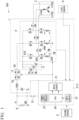
- FIG. 1 is a circuit diagram showing an overall structure (system overall structure) of a vehicle electric power steering device including a semiconductor module according to a first embodiment.
- the vehicle electric power steering device 100 includes, for example, a control unit 1, a motor 2, a first sensor 6, a second sensor 8, a battery 9 (power supply), an ignition switch 10, or the like.
- the control unit 1 includes a semiconductor module 60a (refer to FIG. 2 , described hereinbelow) including a plurality of semiconductor switching elements built therein.
- the control unit 1 includes, for example, a control circuit 3, an inverter circuit 4, a power relay 5, capacitors 7U, 7V, and 7W, or the like.
- the control circuit 3 is connected to the battery 9 with the ignition switch 10 interposed therebetween.
- the control circuit 3 includes, for example, a CPU 30, a drive circuit 31, an input circuit 32, and a power supply circuit 33.
- the power relay 5 is disposed at an upstream side of the inverter circuit 4, that is, disposed between the inverter circuit 4 and the battery 9.
- the power relay 5 includes two switching elements 5a and 5b connected in series to each other.
- the power relay 5 has a relay function of connecting or cutting off between the battery 9 and the inverter circuit 4. That is, the power relay 5 carries out switching power supply to the inverter circuit 4.
- the capacitors 7U, 7V, and 7W are smoothing capacitors and are arranged parallel to each other. Each of the capacitors 7U, 7V, and 7W is connected between a positive electrode and a ground (a negative electrode) of the battery 9.
- the inverter circuit 4 supplies a current to a winding of the motor 2.
- the inverter circuit 4 includes a plurality of switching elements (semiconductor switching element).
- the power relay 5 is connected to the battery 9.
- the inverter circuit 4 includes three bridge circuits corresponding to three-phase windings (U-phase, V-phase, and W-phase) constituting the motor 2.
- the three phases are configured by the same circuit as each other.
- one of phases (the U-phase) will be described, and explanation regarding the V-phase and the W-phase is omitted.
- a high-potential-side switching element 41U and a low-potential-side switching element 42U are connected in series.
- a relay switching element 44U is connected to an intermediate connection portion located between the high-potential-side switching element 41U and the low-potential-side switching element 42U.
- the relay switching element 44U has a relay function of connecting or cutting off between a coil of the motor 2 and the inverter circuit 4 in accordance with a load applied to the coil of the motor 2 or an output from the coil.
- a shunt resistance 43U that detects current is connected to the downstream side of the low-potential-side switching element 42U (on the opposite side of the high-potential-side switching element 41U).
- An end terminal group TM is provided at both ends of the shunt resistance 43U.
- the end terminal group TM is used to detect difference in electrical potential between both ends of the shunt resistance 43U and convert it into a current value.
- a monitor terminal used to detect a state of the inverter circuit 4 (monitor signal) is provided at the inverter circuit 4. The monitor signal is transmitted to the CPU 30 via the input circuit 32 of the control circuit 3.
- the motor 2 is a brushless motor including three phase windings (U-phase, V-phase, and W-phase).
- the U-phase winding, the V-phase winding, and the W-phase winding correspond to the three bridge circuits of the inverter circuit 4.
- the first sensor 6 is a rotation sensor that detects a rotation angle of a motor and is disposed adjacent to the motor 2. A rotation angle signal detected by the first sensor 6 is output from the first sensor 6 and is input to the control circuit 3.
- the second sensor 8 is a torque sensor that detects steering force of the steering wheel, a vehicle speed sensor that detects a speed of a vehicle, or the like.
- the signal detected by the second sensor 8 is output from the second sensor 8 and is input to the control circuit 3.
- the CPU 30 of the control circuit 3 calculates a current value necessary for rotation of the motor 2 and outputs a control signal based on the calculation result to the drive circuit 31.
- the drive circuit 31 drives each of the plurality of the switching elements constituting the inverter circuit 4.
- the inverter circuit 4 detects electrical current and outputs a current detection signal to the control circuit 3.
- the current detection signal is input to the control circuit 3, the control circuit 3 carries out feedback control between the control circuit 3 and the inverter circuit 4.
- All of the switching elements described above are controlled by an output signal of the drive circuit 31 in accordance with a command of the CPU 30.
- the circuit built in the semiconductor module 60a constituting the control unit 1 is not limited to the configuration shown in FIG. 1 .
- the number of the bridge circuits of the inverter circuit 4 built in the semiconductor module 60a may be one to three or greater than or equal to four.
- a circuit excluding the power relay 5, a circuit excluding the shunt resistance 43U, a circuit excluding a part of the switching elements, or the like, may be built in the semiconductor module 60a.
- FIG. 2 is a plan view showing an inner structure of the semiconductor module 60a.
- a resin mold 70 is omitted in the drawing in order to explain the inner structure of the semiconductor module 60a, and an outer-periphery 70a of the resin mold 70 is shown by a dashed-two dotted line.
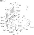
- FIG. 3 is a perspective view showing the semiconductor module 60a.
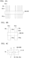
- FIG. 4A is a plan view showing a relevant part of the semiconductor module 60a and is an explanatory view showing a structure of a control terminal 50i.
- FIG. 4B is a plan view showing a relevant part of the semiconductor module 60a and is an explanatory view showing a structure of power terminals 50c and 50e.
- FIG. 4C is an enlarged cross-sectional view showing a relevant part of the semiconductor module 60a and an explanatory view showing a positional relationship between a first support member 60A and the control terminal 50i and a positional relationship between a second support member 60B and the power terminals 50c and 50e.
- the semiconductor module 60a includes the high-potential-side switching element 41U (semiconductor switching element), the low-potential-side switching element 42U (semiconductor switching element), the shunt resistance 43U, the relay switching element 44U (semiconductor switching element), the resin mold 70, and a terminal member 50.
- the resin mold 70 is formed so as to cover the entirety of the semiconductor module 60a.
- the resin mold 70 encloses the switching elements 41U, 42U, and 44U, and the shunt resistance 43U.
- the switching elements 41U, 42U, and 44U, and the shunt resistance 43U are disposed in a region 70b provided at the inside of the outer-periphery 70a of the resin mold 70.
- a known resin is used for a constituent material of the resin mold 70, and the type of materials is not limited.
- the resin mold 70 is formed by molding a resin only on one surface of the terminal member 50.
- the terminal member 50 includes inner terminals 50a, 50g, 50f, 50g, 50h, 50j, and 50k which are disposed inside the resin mold 70, the plurality of the power terminals 50c, 50d, and 50e (outer terminal) which are disposed outside the resin mold 70, and a plurality of control terminals 50i (outer terminal).
- the inner terminal 50a is connected to the relay switching element 44U.
- the inner terminal 50b is connected to the high-potential-side switching element 41U.
- the inner terminal 50f is connected to the low-potential-side switching element 42U.
- the inner terminals 50g, 50h, 50j, and 50k are connected to the control terminals 50i.
- the plurality of the power terminals 50c, 50d, and 50e and the plurality of the control terminals 50i protrude from a side surface 70c of the resin mold 70 (refer to FIG. 3 ). In other words, the power terminals 50c, 50d, and 50e and the control terminals 50i are drawn out from the resin mold 70.
- Connection wirings 45a, 45b, 46a, 46b, 46c are provided inside the resin mold 70.
- connection wiring 45a electrically connects the high-potential-side switching element 41U, the relay switching element 44U, and the inner terminal 50f.
- connection wiring 45b electrically connects the low-potential-side switching element 42U and the inner terminal 50g.
- connection wiring 46a electrically connects the low-potential-side switching element 42U and a first control terminal 50ia serving as one of the plurality of the control terminals 50i.
- connection wiring 46b electrically connects the inner terminal 50a and a second control terminal 50ib serving as one of the plurality of the control terminals 50i.
- connection wiring 46c electrically connects the relay switching element 44U and a third control terminal 50ic serving as one of the plurality of the control terminals 50i.
- connection wiring 46d electrically connects the high-potential-side switching element 41U and a fourth control terminal 50id serving as one of the plurality of the control terminals 50i.
- the shunt resistance 43U electrically connects the inner terminal 50g and the inner terminal 50g.
- the semiconductor module 60a includes a support member 60. At the outside of the resin mold 70, the support member 60 fixes the power terminals 50c and 50e and the control terminals 50i drawn out from the side surface 70c of the resin mold 70.
- the support member 60 includes the first support member 60A that fixes the plurality of the control terminals 50i and the second support member 60B that fixes the power terminals 50c and 50e.
- a known resin is used for a constituent material of the first support member 60A and the second support member 60B, and the type of materials is not limited.
- the first support member 60A is disposed at a position apart from the side surface 70c of the resin mold 70 and extends in a direction in which the plurality of the control terminals 50i are arrayed. That is, the first support member 60A extends in a direction substantially perpendicularly crossing to a direction in which each of the plurality of the control terminals 50i extends.
- the first support member 60A covers part of the outer-periphery of each of the plurality of the control terminals 50i, and fixes the plurality of the control terminals 50i such that the plurality of the control terminals 50i are spaced from each other. In other words, the first support member 60A bundles the plurality of the control terminals 50i and maintains the distance between the control terminals 50i adjacent to each other.
- Each of the plurality of the control terminals 50i has an end portion 50ie located on the opposite side of the side surface 70c of the resin mold 70.
- the first support member 60A is disposed closer to the end portion 50ie than the side surface 70c of the resin mold 70.
- Each of the plurality of the control terminals 50i has a bent portion 50if located between the side surface 70c of the resin mold 70 and the first support member 60A.
- each of the plurality of the control terminals 50i has: a first terminal portion 50ig protruding from the side surface 70c of the resin mold 70; and a second terminal portion 50ih having the end portion 50ie.
- the second terminal portion 50ih is continuous to the first terminal portion 50ig.
- the second terminal portion 50ih has a width smaller than the width of the first terminal portion 50ig in the direction in which the plurality of the control terminals 50i are arrayed.
- the first support member 60A covers part of the outer-periphery of the second terminal portion 50ih, and fixes the second terminal portion 50ih.
- the first support member 60A is disposed at a boundary between the first terminal portion 50ig and the second terminal portion 50ih. In other words, the first support member 60A is formed so as to cover a level-difference portion formed between the first terminal portion 50ig and the second terminal portion 50ih.
- the second support member 60B is disposed at a position apart from the side surface 70c of the resin mold 70 and extends in a direction in which the plurality of the power terminals 50c and 50e are arrayed. That is, the second support member 60B extends in a direction substantially perpendicularly crossing to a direction in which each of the plurality of the power terminals 50c and 50e extends.
- the second support member 60B covers part of the outer-periphery of each of the plurality of the power terminals 50c and 50e, and fixes the plurality of the power terminals 50c and 50e such that the plurality of the power terminals 50c and 50e are spaced from each other. In other words, the second support member 60B bundles the plurality of the power terminals 50c and 50e and maintains the distance between the power terminals 50c and 50e.
- the power terminal 50c has an end portion 50ce located on the opposite side of the side surface 70c of the resin mold 70.
- the power terminal 50e has an end portion 50ee located on the opposite side of the side surface 70c of the resin mold 70.
- the second support member 60B is disposed closer to the end portions 50ce and 50ee than the side surface 70c of the resin mold 70.
- the power terminal 50c has a bent portion 50cf located between the side surface 70c of the resin mold 70 and the second support member 60B.
- the power terminal 50e has a bent portion 50ef located between the side surface 70c of the resin mold 70 and the second support member 60B.
- the power terminal 50c has: a first terminal portion 50cg protruding from the side surface 70c of the resin mold 70; and a second terminal portion 50ch having the end portion 50ce.
- the second terminal portion 50ch is continuous to the first terminal portion 50cg.
- the second terminal portion 50ch has a width smaller than the width of the first terminal portion 50cg in the direction in which the power terminals 50c and 50e are arrayed.
- the power terminal 50e has: a first terminal portion 50eg protruding from the side surface 70c of the resin mold 70; and a second terminal portion 50eh having the end portion 50ee.
- the second terminal portion 50eh is continuous to the first terminal portion 50eg.
- the second terminal portion 50eh has a width smaller than the width of the first terminal portion 50eg in the direction in which the power terminals 50c and 50e are arrayed.
- the power terminal 50d is not shown in FIG. 4B , the same configuration as those of the power terminals 50c and 50e may be applied to the power terminal 50d.
- the power terminal 50d has: a first terminal portion 50dg protruding from the side surface 70c of the resin mold 70; and a second terminal portion 50dh having an end portion 50de.
- the second terminal portion 50dh is continuous to the first terminal portion 50dg.
- the second terminal portion 50dh has a width smaller than the width of the first terminal portion 50dg in a direction in which the plurality of the power terminals are arrayed.
- the second support member 60B covers part of the outer-periphery of the second terminal portions 50ch and 50eh, and fixes the second terminal portions 50ch and 50eh.
- the second support member 60B is disposed at a boundary between the first terminal portion 50cg and the second terminal portion 50ch and is disposed at a boundary between the first terminal portion 50eg and the second terminal portion 50eh.
- the second support member 60B is formed so as to cover a level-difference portion formed between the first terminal portion 50eg and the second terminal portion 50eh and a level-difference portion formed between the first terminal portion 50cg and the second terminal portion 50ch.
- Each of the shapes of the first support member 60A and the second support member 60B is, for example, a rectangular parallelepiped shape.
- the rectangular parallelepiped shape is a shape having a long side extending in the direction of the side of the resin mold 70.
- Each of the first support member 60A and the second support member 60B is disposed parallel to the side surface 70c of the resin mold 70.
- a center position P1 of the first support member 60A coincides with a center position P2 of the control terminal 50i.
- the thickness of the first support member 60A is greater than or equal to the thickness of the control terminal 50i. That is, the thickness of the first support member 60A and the thickness of the control terminal 50i are determined such that the structure of the first support member 60A and the structure of the control terminal 50i are symmetrical with respect to the center line C passing through the center positions P1 and P2.
- the center position of the second support member 60B coincides with the center position of each of the power terminals 50c and 50e.
- the thickness of the second support member 60B is greater than or equal to the thickness of each of the power terminals 50c and 50e. That is, the power terminals 50c and 50e is fixed by the second support member 60B such that the second support member 60B and the power terminals 50c and 50e are symmetrical with respect to the center line C passing through the center positions P1 and P2.
- Each of the plurality of the control terminals 50i has two first surfaces F and two second surfaces S.
- the first surface F is a surface parallel to the direction (reference numeral D3 shown in FIG. 3 ) orthogonal to the direction in which the control terminal 50i extends (reference numeral D1 shown in FIG. 3 ) and the direction in which the control terminals 50i are arrayed (reference numeral D2 shown in FIG. 3 ).
- the second surface S is a surface parallel to the direction in which the control terminals 50i are arrayed (reference numeral D2 shown in FIG. 3 ).
- the first support member 60A covers the two first surfaces F and the two second surfaces S of each of the plurality of the control terminals 50i.
- each of the power terminals 50c and 50e has two first surfaces F and two second surfaces S.
- the first surface F is a surface parallel to the direction (reference numeral E3 shown in FIG. 3 ) orthogonal to the direction in which the power terminals 50c and 50e extend (reference numeral E1 shown in FIG. 3 ) and the direction in which the power terminals 50c and 50e are arrayed (reference numeral E2 shown in FIG. 3 ).
- the second surface S is a surface parallel to the direction in which the power terminals 50c and 50e are arrayed (reference numeral E2 shown in FIG. 3 ).
- the second support member 60B covers the two first surfaces F and the two second surfaces S of each of the power terminals 50c and 50e.
- the thickness of the support member 60 is less than or equal to the thickness of the resin mold 70.
- the support member 60 only fixes the control terminals 50i and the power terminals 50c and 50e, and a pressure applied to the support member 60 is low, as compared to the resin mold 70 covering the plurality of the semiconductor switching elements, the terminal members, and the connection wirings.
- FIGS. 5A and 5B are enlarged cross-sectional views showing a relevant part of the semiconductor module 60a and are views showing a step of bending the outer terminal.
- the first support member 60A is formed at the plurality of the control terminals 50i.
- the position at which the first support member 60A is formed is a position closer to the end portion 50ie than the side surface 70c of the resin mold 70. Consequently, the plurality of the control terminals 50i is bundled together by the first support member 60A.
- a jig 200 is disposed under the control terminal 50i, and the jig 200 moves upward from the lower side.
- the jig 200 comes into contact with the control terminal 50i.
- the jig 200 bends the control terminal 50i in accordance with the upward movement of the jig 200. Therefore, the bent portion 50if is formed at the control terminal 50i between the side surface 70c of the resin mold 70 and the first support member 60A.
- the plurality of the control terminals 50i can be bundled together by the first support member 60A.
- the plurality of the power terminals 50c and 50e can be bundled together by the second support member 60B. Consequently, deformation of the terminal member 50 is suppressed when working the terminal member 50, and it is possible to stabilize the size of each of the plurality of the control terminals 50i and the plurality of the power terminals 50c and 50e after machining.
- each of the first support member 60A and the second support member 60B has the rectangular parallelepiped shape, the shape of each of the first support member 60A and the second support member 60B can be the minimum size. Consequently, the shape of the semiconductor module 60a attached to each of the first support member 60A and the second support member 60B can be downsized.
- the center position of the support member 60 coincides with the center positions of the outer terminals (the control terminals 50i and the power terminals 50c and 50e) in the thickness direction TH. For this reason, deformation of the support member 60 such as warpage, torsion, or the like is suppressed, and it is possible to stabilize accuracy of dimensions of the control terminals 50i and the power terminals 50c and 50e.
- the outer terminals (the control terminals 50i and the power terminals 50c and 50e) are fixed by the support member 60, a stress applied to the outer terminals can be absorbed by the support member 60 when cutting the outer terminals in the step of manufacturing the semiconductor module 60a. Accordingly, the resin forming the resin mold 70 is suppressed from being peeled off from the outer terminals in the step of forming the resin mold 70 and the outer terminals. Moreover, due to provision of the support member 60, deformation of the outer terminal such as torsion, twist, or the like can be suppressed in the step of forming the outer terminals.
- the first support member 60A is disposed closer to the end portion 50ie than the side surface 70c of the resin mold 70 in the first embodiment.
- the second support member 60B is disposed closer to the end portions 50ce and 50ee than the side surface 70c of the resin mold 70. Consequently, even in a case in which the positions of the outer terminals (the control terminals 50i and the power terminals 50c and 50e) are displaced in the step of forming the semiconductor module 60a, an effect of restoring the positions of the outer terminals to original positions by the support member 60 (the first support member 60A and the second support member 60B), that is, an effect of rectifying the positions of the outer terminals can be obtained.
- the support member 60 (the first support member 60A and the second support member 60B) extends in a direction in which the plurality of the outer terminals (the control terminals 50i and the power terminals 50c and 50e) are arrayed. Additionally, the support member 60 is not formed at a portion at which the outer terminal is not formed. Therefore, the length of the support member 60 can be shorter, and it contributes to downsizing of the semiconductor module 60a.
- the first support member 60A covers the two first surfaces F and the two second surfaces S of each of the plurality of the control terminals 50i, it is possible to suppress deformation of the plurality of the control terminals 50i in the direction parallel to each of the first surface F and the second surface S.
- the second support member 60B covers the two first surfaces F and the two second surfaces S of each of the power terminals 50c and 50e, it is possible to suppress deformation of the power terminals 50c and 50e in the direction parallel to each of the first surface F and the second surface S.
- the first support member 60A is disposed closer to the end portion 50ie than the side surface 70c of the resin mold 70, it is possible to avoid interference such that the jig 200 comes into contact with the first support member 60A even in a case of forming the bent portion 50if by using the jig 200.
- the material of the support member 60 (the first support member 60A and the second support member 60B) is the same as the material of the resin mold 70.
- the support member 60 can be formed by using the same material as that of the resin mold 70. That is, the resin mold 70 and the support member 60 can be formed in the same step. Therefore, it is not necessary to form the support member 60 in the step different from the step of forming the resin mold 70. Accordingly, it is possible to omit a step of forming only the support member 60.
- the modified example 2 is different from the first embodiment in that the resin mold 70 has a rectangular shape.
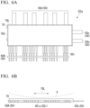
- FIG. 6A is a plan view showing a semiconductor module 61a.
- FIG. 6B is a side view showing the semiconductor module 61a.
- reference letter X shown in FIG. 6B schematically shows a case in which warpage occurs on the resin mold 70 during molding the resin mold 70.
- the resin mold 70 having the rectangular shape has a long side 70L and a short side 70S when viewed in a plan view.
- the first support member 60A (60) extends along the long side 70L and fixes the plurality of the control terminals 50i and bundles them together.
- Warpage may occur on the resin mold 70 during molding the resin mold 70.
- the warpage is likely to occur in the direction of the long side 70L of the resin mold 70 as shown by reference letter X.
- the positions of the end portions 50ie of the control terminals 50i may be displaced.
- FIG. 7 is a perspective view showing a semiconductor module 62a according to the second embodiment.
- the second embodiment is different from the aforementioned first embodiment in that the resin mold 70 has the rectangular shape and a plurality of outer terminals are arrayed in two rows.
- the semiconductor module 62a includes the resin mold 70 having the rectangular shape, the plurality of the control terminals 50i, and the power terminals 50c, 50d, and 50e.
- the plurality of the control terminals 50i and the power terminals 50c, 50d, and 50e are drawn out from one long side 70L constituting the resin mold 70.
- the plurality of the control terminals 50i (first outer terminal) constitute a first terminal group 55 including a plurality of outer terminals arranged in a first row.
- Each of the plurality of the control terminals 50i has the bent portion 50if (first bent portion) located between the side surface 70c of the resin mold 70 and the first support member 60A.
- the first support member 60A fixes the plurality of the control terminals 50i and bundles them together such that the plurality of the control terminals 50i constituting the first terminal group 55 are spaced from each other.
- the power terminals 50c, 50d, and 50e constitute a second terminal group 56 including a plurality of outer terminals arranged in a second row.
- the power terminals 50c, 50d, and 50e have the bent portions 50cf, 50df, and 50ef (second bent portion), respectively, which are located between the side surface 70c of the resin mold 70 and the second support member 60B.
- the second support member 60B fixes the power terminals 50c, 50d, and 50e and bundles them together such that the power terminals 50c, 50d, and 50e constituting the second terminal group 56 are spaced from each other.
- the second support member 60B is formed so as to cover the level-difference portion formed between the first terminal portion 50eg and the second terminal portion 50eh and the level-difference portion formed between the first terminal portion 50cg and the second terminal portion SOch. Consequently, the second support member 608 is caught and fixed by the level-difference portion.
- the distances from the side surface 70c of the resin mold 70 to the bent portions 50cf, 50df, and 50ef are greater than the distance from the side surface 70c of the resin mold 70 to the bent portion 50if. Additionally, the first support member 60A and the second support member 60B are parallel to each other.
- the plurality of the control terminals 50i can be fixed and bundled together by the first support member 60A.
- the plurality of the power terminals 50c, 50d, and 50e can be fixed and bundled together by the second support member 60B. Consequently, deformation of the terminal member 50 is suppressed when working the terminal member 50, and it is possible to stabilize the size of each of the plurality of the control terminals 50i and the plurality of the power terminals 50c, 50d, and 50e after machining. Furthermore, it is possible to obtain the effect the same as or similar to that of the above-mentioned first embodiment.
- a support member may be provided so as to correspond to the positions of the bent portions 50cf, 50df, and 50ef. With this configuration, even the case in which the plurality of the bent portions are arrayed, it is possible to rectify the positions of the bent portions of the plurality of the power terminals 50c, 50d, and 50e by the support member.
- FIG. 8 is a perspective view showing a semiconductor module according to a third embodiment.
- the third embodiment is different from the aforementioned second embodiment in that the plurality of the outer terminals arrayed in two rows are fixed by one support member 60.
- a semiconductor module 63a includes the resin mold 70 having the rectangular shape, the plurality of the control terminals 50i, and the power terminals 50c, 50d, and 50e.
- the plurality of the control terminals 50i and the power terminals 50c, 50d, and 50e are drawn out from one long side 70L constituting the resin mold 70.
- the plurality of the control terminals 50i (first outer terminal) constitute the first terminal group 55 including a plurality of outer terminals arranged in the first row.
- Each of the plurality of the control terminals 50i has the bent portion 50if (first bent portion) located between the side surface 70c of the resin mold 70 and the support member 60.
- the power terminals 50c, 50d, and 50e (second outer terminal) and the plurality of the control terminals 50i (second outer terminal) constitute the second terminal group 56 including a plurality of outer terminals arranged in the second row.
- the power terminals 50c, 50d, and 50e have the bent portions 50cf, 50df, and 50ef (second bent portion), respectively, which are located between the side surface 70c of the resin mold 70 and the support member 60.
- each of the plurality of the control terminals 50i arranged in the second row has a bent portion 50ii (second bent portion) located between the side surface 70c of the resin mold 70 and the support member 60.
- the distances from the side surface 70c of the resin mold 70 to the bent portions 50cf, 50df, 50ef, and 50ii are greater than the distance from the side surface 70c of the resin mold 70 to the bent portion 50if.
- the support member 60 fixes the plurality of the control terminals 50i constituting the first terminal group 55, the power terminals 50c, 50d, and 50e constituting the second terminal group 56, and the plurality of the control terminals 50i and bundles them together such that they are spaced from each other.
- the plurality of the control terminals 50i and the plurality of the power terminals 50c, 50d, and 50e can be fixed and bundled together by one support member 60A. Consequently, deformation of the terminal member 50 is suppressed when working the terminal member 50, and it is possible to stabilize the size of each of the plurality of the control terminals 50i and the plurality of the power terminals 50c, 50d, and 50e after machining. Furthermore, it is possible to obtain the effect the same as or similar to that of the above-mentioned first embodiment.
- the number of the support members 60 is one, the number of support members can be reduced. Since the plurality of the control terminals 50i and the plurality of the power terminals 50c, 50d, and 50e can be collectively bundled together, it is possible to improve accuracy of the dimensions thereof.
- terminal member 50a, 50b, 50f, 50g, 50h...inner terminal, 50c, 50d, 50e...power terminal, 50ce, 50de, 50ee, 50ie...end portion, 50cf, 50df, 50ef, 50if, 50ii...bent portion, 50cg, 50dg, 50eg...first terminal portion, 50dh, 50ch, 50eh...second terminal portion, 50i...control terminal, 50ia...first control terminal (control terminal), 50ib...second control terminal (control terminal), 50ic...third control terminal (control terminal), 50id...fourth control terminal (control terminal), 50ig...first terminal portion, 50ih...second terminal portion, 50j, 50k...inner terminal, 55 ...
Landscapes
- Engineering & Computer Science (AREA)
- Power Engineering (AREA)
- Inverter Devices (AREA)
- Structures Or Materials For Encapsulating Or Coating Semiconductor Devices Or Solid State Devices (AREA)
Abstract
Description
- The present disclosure relates to a semiconductor module.
- A conventional semiconductor module is described in
Patent Literatures - In
Patent Literature 1, a three-dimensional structure having a control terminal and a power terminal which are bent is described. InPatent Literature 2, a member that is formed around a terminal and made of a high thermal conductive resin is described. -
- [Patent Document 1]
Japanese Patent No. 4336713 - [Patent Document 2]
Japanese Patent No. 4979909 - In the structure of
Patent Literatures - The present disclosure was made in order to solve the above problem and has an object to provide a semiconductor module can suppress positional displacement or deformation of a terminal.
- A semiconductor module according to the present disclosure includes: a plurality of semiconductor switching elements; a resin mold having a side surface and surrounding the plurality of the semiconductor switching elements; a terminal member having a plurality of inner terminals electrically connected to the plurality of the semiconductor switching elements inside the resin mold and a plurality of outer terminals protruding from the side surface of the resin mold; and a support member disposed at a position apart from the side surface of the resin mold, the support member extending in a direction in which the plurality of the outer terminals are arrayed, the support member covering a part of an outer-periphery of each of the plurality of the outer terminals, the support member fixing the plurality of the outer terminals such that the plurality of the outer terminals are spaced from each other.
- According to the present disclosure, it is possible to provide a semiconductor module can suppress positional displacement or deformation of a terminal.
-
-
FIG. 1 is a circuit diagram showing an overall structure of a vehicle electric power steering device including a semiconductor module according to a first embodiment. -
FIG. 2 is a plan view showing is an inner structure of the semiconductor module according to the first embodiment. -
FIG. 3 is a perspective view showing the semiconductor module according to the first embodiment. -
FIG. 4A is a plan view showing a relevant part of the semiconductor module according to the first embodiment. -
FIG. 4B is a plan view showing a relevant part of the semiconductor module according to the first embodiment. -
FIG. 4C is an enlarged cross-sectional view showing a relevant part of the semiconductor module according to the first embodiment. -
FIG. 5A is an enlarged cross-sectional view showing a relevant part of the semiconductor module according to the first embodiment and showing a step of bending terminals. -
FIG. 5B is an enlarged cross-sectional view showing a relevant part of the semiconductor module according to the first embodiment and showing a step of bending terminals. -
FIG. 6A is a plan view showing a semiconductor module according to a modified example of the first embodiment. -
FIG. 6B is a side view showing the semiconductor module according to the modified example of the first embodiment. -
FIG. 7 is a perspective view showing a semiconductor module according to a second embodiment. -
FIG. 8 is a perspective view showing a semiconductor module according to a third embodiment. -
FIG. 1 is a circuit diagram showing an overall structure (system overall structure) of a vehicle electric power steering device including a semiconductor module according to a first embodiment. - The vehicle electric
power steering device 100 includes, for example, acontrol unit 1, amotor 2, afirst sensor 6, a second sensor 8, a battery 9 (power supply), anignition switch 10, or the like. - The
control unit 1 includes asemiconductor module 60a (refer toFIG. 2 , described hereinbelow) including a plurality of semiconductor switching elements built therein. - The
control unit 1 includes, for example, acontrol circuit 3, an inverter circuit 4, apower relay 5,capacitors - The
control circuit 3 is connected to the battery 9 with theignition switch 10 interposed therebetween. Thecontrol circuit 3 includes, for example, aCPU 30, adrive circuit 31, aninput circuit 32, and apower supply circuit 33. - The
power relay 5 is disposed at an upstream side of the inverter circuit 4, that is, disposed between the inverter circuit 4 and the battery 9. Thepower relay 5 includes twoswitching elements power relay 5 has a relay function of connecting or cutting off between the battery 9 and the inverter circuit 4. That is, thepower relay 5 carries out switching power supply to the inverter circuit 4. - The
capacitors capacitors - The inverter circuit 4 supplies a current to a winding of the
motor 2. - The inverter circuit 4 includes a plurality of switching elements (semiconductor switching element). The
power relay 5 is connected to the battery 9. The inverter circuit 4 includes three bridge circuits corresponding to three-phase windings (U-phase, V-phase, and W-phase) constituting themotor 2. - The three phases are configured by the same circuit as each other. In the following explanation, one of phases (the U-phase) will be described, and explanation regarding the V-phase and the W-phase is omitted.
- In the inverter circuit 4, a high-potential-
side switching element 41U and a low-potential-side switching element 42U are connected in series. Arelay switching element 44U is connected to an intermediate connection portion located between the high-potential-side switching element 41U and the low-potential-side switching element 42U. Therelay switching element 44U has a relay function of connecting or cutting off between a coil of themotor 2 and the inverter circuit 4 in accordance with a load applied to the coil of themotor 2 or an output from the coil. - A
shunt resistance 43U that detects current is connected to the downstream side of the low-potential-side switching element 42U (on the opposite side of the high-potential-side switching element 41U). - An end terminal group TM is provided at both ends of the
shunt resistance 43U. The end terminal group TM is used to detect difference in electrical potential between both ends of theshunt resistance 43U and convert it into a current value. A monitor terminal used to detect a state of the inverter circuit 4 (monitor signal) is provided at the inverter circuit 4. The monitor signal is transmitted to theCPU 30 via theinput circuit 32 of thecontrol circuit 3. - The
motor 2 is a brushless motor including three phase windings (U-phase, V-phase, and W-phase). The U-phase winding, the V-phase winding, and the W-phase winding correspond to the three bridge circuits of the inverter circuit 4. - The
first sensor 6 is a rotation sensor that detects a rotation angle of a motor and is disposed adjacent to themotor 2. A rotation angle signal detected by thefirst sensor 6 is output from thefirst sensor 6 and is input to thecontrol circuit 3. - The second sensor 8 is a torque sensor that detects steering force of the steering wheel, a vehicle speed sensor that detects a speed of a vehicle, or the like. The signal detected by the second sensor 8 is output from the second sensor 8 and is input to the
control circuit 3. - The
CPU 30 of thecontrol circuit 3 calculates a current value necessary for rotation of themotor 2 and outputs a control signal based on the calculation result to thedrive circuit 31. Thedrive circuit 31 drives each of the plurality of the switching elements constituting the inverter circuit 4. - The inverter circuit 4 detects electrical current and outputs a current detection signal to the
control circuit 3. The current detection signal is input to thecontrol circuit 3, thecontrol circuit 3 carries out feedback control between thecontrol circuit 3 and the inverter circuit 4. - All of the switching elements described above are controlled by an output signal of the
drive circuit 31 in accordance with a command of theCPU 30. - Note that, the circuit built in the
semiconductor module 60a constituting thecontrol unit 1 is not limited to the configuration shown inFIG. 1 . For example, the number of the bridge circuits of the inverter circuit 4 built in thesemiconductor module 60a may be one to three or greater than or equal to four. Furthermore, a circuit excluding thepower relay 5, a circuit excluding theshunt resistance 43U, a circuit excluding a part of the switching elements, or the like, may be built in thesemiconductor module 60a. -
FIG. 2 is a plan view showing an inner structure of thesemiconductor module 60a. InFIG. 2 , aresin mold 70 is omitted in the drawing in order to explain the inner structure of thesemiconductor module 60a, and an outer-periphery 70a of theresin mold 70 is shown by a dashed-two dotted line. -
FIG. 3 is a perspective view showing thesemiconductor module 60a. -
FIG. 4A is a plan view showing a relevant part of thesemiconductor module 60a and is an explanatory view showing a structure of acontrol terminal 50i. -
FIG. 4B is a plan view showing a relevant part of thesemiconductor module 60a and is an explanatory view showing a structure ofpower terminals -
FIG. 4C is an enlarged cross-sectional view showing a relevant part of thesemiconductor module 60a and an explanatory view showing a positional relationship between afirst support member 60A and thecontrol terminal 50i and a positional relationship between asecond support member 60B and thepower terminals - The
semiconductor module 60a includes the high-potential-side switching element 41U (semiconductor switching element), the low-potential-side switching element 42U (semiconductor switching element), theshunt resistance 43U, therelay switching element 44U (semiconductor switching element), theresin mold 70, and aterminal member 50. - The
resin mold 70 is formed so as to cover the entirety of thesemiconductor module 60a. Theresin mold 70 encloses the switchingelements shunt resistance 43U. In other words, the switchingelements shunt resistance 43U are disposed in aregion 70b provided at the inside of the outer-periphery 70a of theresin mold 70. - A known resin is used for a constituent material of the
resin mold 70, and the type of materials is not limited. Theresin mold 70 is formed by molding a resin only on one surface of theterminal member 50. - The
terminal member 50 includesinner terminals resin mold 70, the plurality of thepower terminals resin mold 70, and a plurality ofcontrol terminals 50i (outer terminal). - The
inner terminal 50a is connected to therelay switching element 44U. Theinner terminal 50b is connected to the high-potential-side switching element 41U. Theinner terminal 50f is connected to the low-potential-side switching element 42U. Theinner terminals control terminals 50i. - The plurality of the
power terminals control terminals 50i protrude from aside surface 70c of the resin mold 70 (refer toFIG. 3 ). In other words, thepower terminals control terminals 50i are drawn out from theresin mold 70. -
Connection wirings resin mold 70. - The
connection wiring 45a electrically connects the high-potential-side switching element 41U, therelay switching element 44U, and theinner terminal 50f. - The
connection wiring 45b electrically connects the low-potential-side switching element 42U and theinner terminal 50g. - The
connection wiring 46a electrically connects the low-potential-side switching element 42U and a first control terminal 50ia serving as one of the plurality of thecontrol terminals 50i. - The
connection wiring 46b electrically connects theinner terminal 50a and a second control terminal 50ib serving as one of the plurality of thecontrol terminals 50i. - The
connection wiring 46c electrically connects therelay switching element 44U and a third control terminal 50ic serving as one of the plurality of thecontrol terminals 50i. - The
connection wiring 46d electrically connects the high-potential-side switching element 41U and a fourth control terminal 50id serving as one of the plurality of thecontrol terminals 50i. - The
shunt resistance 43U electrically connects theinner terminal 50g and theinner terminal 50g. - As shown in
FIG. 3 , thesemiconductor module 60a includes asupport member 60. At the outside of theresin mold 70, thesupport member 60 fixes thepower terminals control terminals 50i drawn out from theside surface 70c of theresin mold 70. - Specifically, the
support member 60 includes thefirst support member 60A that fixes the plurality of thecontrol terminals 50i and thesecond support member 60B that fixes thepower terminals first support member 60A and thesecond support member 60B, and the type of materials is not limited. - The
first support member 60A is disposed at a position apart from theside surface 70c of theresin mold 70 and extends in a direction in which the plurality of thecontrol terminals 50i are arrayed. That is, thefirst support member 60A extends in a direction substantially perpendicularly crossing to a direction in which each of the plurality of thecontrol terminals 50i extends. Thefirst support member 60A covers part of the outer-periphery of each of the plurality of thecontrol terminals 50i, and fixes the plurality of thecontrol terminals 50i such that the plurality of thecontrol terminals 50i are spaced from each other. In other words, thefirst support member 60A bundles the plurality of thecontrol terminals 50i and maintains the distance between thecontrol terminals 50i adjacent to each other. - Each of the plurality of the
control terminals 50i has an end portion 50ie located on the opposite side of theside surface 70c of theresin mold 70. Thefirst support member 60A is disposed closer to the end portion 50ie than theside surface 70c of theresin mold 70. - Each of the plurality of the
control terminals 50i has a bent portion 50if located between theside surface 70c of theresin mold 70 and thefirst support member 60A. - As shown in
FIG. 4A , each of the plurality of thecontrol terminals 50i has: a first terminal portion 50ig protruding from theside surface 70c of theresin mold 70; and a second terminal portion 50ih having the end portion 50ie. The second terminal portion 50ih is continuous to the first terminal portion 50ig. The second terminal portion 50ih has a width smaller than the width of the first terminal portion 50ig in the direction in which the plurality of thecontrol terminals 50i are arrayed. - The
first support member 60A covers part of the outer-periphery of the second terminal portion 50ih, and fixes the second terminal portion 50ih. Thefirst support member 60A is disposed at a boundary between the first terminal portion 50ig and the second terminal portion 50ih. In other words, thefirst support member 60A is formed so as to cover a level-difference portion formed between the first terminal portion 50ig and the second terminal portion 50ih. - The
second support member 60B is disposed at a position apart from theside surface 70c of theresin mold 70 and extends in a direction in which the plurality of thepower terminals second support member 60B extends in a direction substantially perpendicularly crossing to a direction in which each of the plurality of thepower terminals second support member 60B covers part of the outer-periphery of each of the plurality of thepower terminals power terminals power terminals second support member 60B bundles the plurality of thepower terminals power terminals - The
power terminal 50c has an end portion 50ce located on the opposite side of theside surface 70c of theresin mold 70. Thepower terminal 50e has an end portion 50ee located on the opposite side of theside surface 70c of theresin mold 70. Thesecond support member 60B is disposed closer to the end portions 50ce and 50ee than theside surface 70c of theresin mold 70. - The
power terminal 50c has a bent portion 50cf located between theside surface 70c of theresin mold 70 and thesecond support member 60B. - The
power terminal 50e has a bent portion 50ef located between theside surface 70c of theresin mold 70 and thesecond support member 60B. - As shown in
FIG. 4B , thepower terminal 50c has: a first terminal portion 50cg protruding from theside surface 70c of theresin mold 70; and a second terminal portion 50ch having the end portion 50ce. The second terminal portion 50ch is continuous to the first terminal portion 50cg. The second terminal portion 50ch has a width smaller than the width of the first terminal portion 50cg in the direction in which thepower terminals - The
power terminal 50e has: a first terminal portion 50eg protruding from theside surface 70c of theresin mold 70; and a second terminal portion 50eh having the end portion 50ee. The second terminal portion 50eh is continuous to the first terminal portion 50eg. The second terminal portion 50eh has a width smaller than the width of the first terminal portion 50eg in the direction in which thepower terminals - Note that, although the
power terminal 50d is not shown inFIG. 4B , the same configuration as those of thepower terminals power terminal 50d. - In this case, the
power terminal 50d has: a first terminal portion 50dg protruding from theside surface 70c of theresin mold 70; and a second terminal portion 50dh having an end portion 50de. The second terminal portion 50dh is continuous to the first terminal portion 50dg. The second terminal portion 50dh has a width smaller than the width of the first terminal portion 50dg in a direction in which the plurality of the power terminals are arrayed. - The
second support member 60B covers part of the outer-periphery of the second terminal portions 50ch and 50eh, and fixes the second terminal portions 50ch and 50eh. Thesecond support member 60B is disposed at a boundary between the first terminal portion 50cg and the second terminal portion 50ch and is disposed at a boundary between the first terminal portion 50eg and the second terminal portion 50eh. In other words, thesecond support member 60B is formed so as to cover a level-difference portion formed between the first terminal portion 50eg and the second terminal portion 50eh and a level-difference portion formed between the first terminal portion 50cg and the second terminal portion 50ch. - Each of the shapes of the
first support member 60A and thesecond support member 60B is, for example, a rectangular parallelepiped shape. Here, the rectangular parallelepiped shape is a shape having a long side extending in the direction of the side of theresin mold 70. Each of thefirst support member 60A and thesecond support member 60B is disposed parallel to theside surface 70c of theresin mold 70. - As shown in
FIG. 4C , in the thickness direction TH of thefirst support member 60A, a center position P1 of thefirst support member 60A coincides with a center position P2 of thecontrol terminal 50i. Moreover, the thickness of thefirst support member 60A is greater than or equal to the thickness of thecontrol terminal 50i. That is, the thickness of thefirst support member 60A and the thickness of thecontrol terminal 50i are determined such that the structure of thefirst support member 60A and the structure of thecontrol terminal 50i are symmetrical with respect to the center line C passing through the center positions P1 and P2. - Similarly, also in the thickness direction of the
second support member 60B, the center position of thesecond support member 60B coincides with the center position of each of thepower terminals second support member 60B is greater than or equal to the thickness of each of thepower terminals power terminals second support member 60B such that thesecond support member 60B and thepower terminals - Each of the plurality of the
control terminals 50i has two first surfaces F and two second surfaces S. The first surface F is a surface parallel to the direction (reference numeral D3 shown inFIG. 3 ) orthogonal to the direction in which thecontrol terminal 50i extends (reference numeral D1 shown inFIG. 3 ) and the direction in which thecontrol terminals 50i are arrayed (reference numeral D2 shown inFIG. 3 ). The second surface S is a surface parallel to the direction in which thecontrol terminals 50i are arrayed (reference numeral D2 shown inFIG. 3 ). Thefirst support member 60A covers the two first surfaces F and the two second surfaces S of each of the plurality of thecontrol terminals 50i. - Similarly, each of the
power terminals FIG. 3 ) orthogonal to the direction in which thepower terminals FIG. 3 ) and the direction in which thepower terminals FIG. 3 ). The second surface S is a surface parallel to the direction in which thepower terminals FIG. 3 ). Thesecond support member 60B covers the two first surfaces F and the two second surfaces S of each of thepower terminals - Note that, the thickness of the
support member 60 is less than or equal to the thickness of theresin mold 70. - This is because, the
support member 60 only fixes thecontrol terminals 50i and thepower terminals support member 60 is low, as compared to theresin mold 70 covering the plurality of the semiconductor switching elements, the terminal members, and the connection wirings. - Next, a step of forming a bent portion by bending an outer terminal will be described with reference to
FIGS. 5A and 5B . -
FIGS. 5A and 5B are enlarged cross-sectional views showing a relevant part of thesemiconductor module 60a and are views showing a step of bending the outer terminal. - In the following explanation, a step of bending the
control terminal 50i will be described. Since a step of bending thepower terminals control terminal 50i, the explanation therefor is omitted. - First of all, as shown in
FIG. 5A , thefirst support member 60A is formed at the plurality of thecontrol terminals 50i. The position at which thefirst support member 60A is formed is a position closer to the end portion 50ie than theside surface 70c of theresin mold 70. Consequently, the plurality of thecontrol terminals 50i is bundled together by thefirst support member 60A. - Next, a
jig 200 is disposed under thecontrol terminal 50i, and thejig 200 moves upward from the lower side. Thejig 200 comes into contact with thecontrol terminal 50i. Furthermore, thejig 200 bends thecontrol terminal 50i in accordance with the upward movement of thejig 200. Therefore, the bent portion 50if is formed at thecontrol terminal 50i between theside surface 70c of theresin mold 70 and thefirst support member 60A. - According to the
semiconductor module 60a of the first embodiment, the plurality of thecontrol terminals 50i can be bundled together by thefirst support member 60A. The plurality of thepower terminals second support member 60B. Consequently, deformation of theterminal member 50 is suppressed when working theterminal member 50, and it is possible to stabilize the size of each of the plurality of thecontrol terminals 50i and the plurality of thepower terminals - Furthermore, since each of the
first support member 60A and thesecond support member 60B has the rectangular parallelepiped shape, the shape of each of thefirst support member 60A and thesecond support member 60B can be the minimum size. Consequently, the shape of thesemiconductor module 60a attached to each of thefirst support member 60A and thesecond support member 60B can be downsized. - Additionally, the center position of the support member 60 (the
first support member 60A and thesecond support member 60B) coincides with the center positions of the outer terminals (thecontrol terminals 50i and thepower terminals support member 60 such as warpage, torsion, or the like is suppressed, and it is possible to stabilize accuracy of dimensions of thecontrol terminals 50i and thepower terminals - Moreover, since the outer terminals (the
control terminals 50i and thepower terminals support member 60, a stress applied to the outer terminals can be absorbed by thesupport member 60 when cutting the outer terminals in the step of manufacturing thesemiconductor module 60a. Accordingly, the resin forming theresin mold 70 is suppressed from being peeled off from the outer terminals in the step of forming theresin mold 70 and the outer terminals. Moreover, due to provision of thesupport member 60, deformation of the outer terminal such as torsion, twist, or the like can be suppressed in the step of forming the outer terminals. - Furthermore, the
first support member 60A is disposed closer to the end portion 50ie than theside surface 70c of theresin mold 70 in the first embodiment. In addition, thesecond support member 60B is disposed closer to the end portions 50ce and 50ee than theside surface 70c of theresin mold 70. Consequently, even in a case in which the positions of the outer terminals (thecontrol terminals 50i and thepower terminals semiconductor module 60a, an effect of restoring the positions of the outer terminals to original positions by the support member 60 (thefirst support member 60A and thesecond support member 60B), that is, an effect of rectifying the positions of the outer terminals can be obtained. - The support member 60 (the
first support member 60A and thesecond support member 60B) extends in a direction in which the plurality of the outer terminals (thecontrol terminals 50i and thepower terminals support member 60 is not formed at a portion at which the outer terminal is not formed. Therefore, the length of thesupport member 60 can be shorter, and it contributes to downsizing of thesemiconductor module 60a. - Since the
first support member 60A covers the two first surfaces F and the two second surfaces S of each of the plurality of thecontrol terminals 50i, it is possible to suppress deformation of the plurality of thecontrol terminals 50i in the direction parallel to each of the first surface F and the second surface S. - Similarly, the
second support member 60B covers the two first surfaces F and the two second surfaces S of each of thepower terminals power terminals - Furthermore, as shown in
FIGS. 5A and 5B , since thefirst support member 60A is disposed closer to the end portion 50ie than theside surface 70c of theresin mold 70, it is possible to avoid interference such that thejig 200 comes into contact with thefirst support member 60A even in a case of forming the bent portion 50if by using thejig 200. - In the modified example 1, the material of the support member 60 (the
first support member 60A and thesecond support member 60B) is the same as the material of theresin mold 70. - Consequently, when forming the
resin mold 70, thesupport member 60 can be formed by using the same material as that of theresin mold 70. That is, theresin mold 70 and thesupport member 60 can be formed in the same step. Therefore, it is not necessary to form thesupport member 60 in the step different from the step of forming theresin mold 70. Accordingly, it is possible to omit a step of forming only thesupport member 60. - The modified example 2 is different from the first embodiment in that the
resin mold 70 has a rectangular shape. -
FIG. 6A is a plan view showing asemiconductor module 61a.FIG. 6B is a side view showing thesemiconductor module 61a. Furthermore, reference letter X shown inFIG. 6B schematically shows a case in which warpage occurs on theresin mold 70 during molding theresin mold 70. - Note that, in
FIG. 6A , thesecond support member 60B is omitted. - As shown in
FIG. 6A , theresin mold 70 having the rectangular shape has along side 70L and ashort side 70S when viewed in a plan view. - The
first support member 60A (60) extends along thelong side 70L and fixes the plurality of thecontrol terminals 50i and bundles them together. - Warpage may occur on the
resin mold 70 during molding theresin mold 70. The warpage is likely to occur in the direction of thelong side 70L of theresin mold 70 as shown by reference letter X. When the foregoing warpage occurs on theresin mold 70, the positions of the end portions 50ie of thecontrol terminals 50i may be displaced. - In contrast, as shown in
FIG. 6B , since thefirst support member 60A is provided in the modified example 2, such warpage is suppressed from occurring on theresin mold 70 by thefirst support member 60A even in the case in which theresin mold 70 has the rectangular shape. -
FIG. 7 is a perspective view showing asemiconductor module 62a according to the second embodiment. - The second embodiment is different from the aforementioned first embodiment in that the
resin mold 70 has the rectangular shape and a plurality of outer terminals are arrayed in two rows. - As shown in
FIG. 7 , thesemiconductor module 62a includes theresin mold 70 having the rectangular shape, the plurality of thecontrol terminals 50i, and thepower terminals control terminals 50i and thepower terminals long side 70L constituting theresin mold 70. - The plurality of the
control terminals 50i (first outer terminal) constitute a firstterminal group 55 including a plurality of outer terminals arranged in a first row. Each of the plurality of thecontrol terminals 50i has the bent portion 50if (first bent portion) located between theside surface 70c of theresin mold 70 and thefirst support member 60A. Thefirst support member 60A fixes the plurality of thecontrol terminals 50i and bundles them together such that the plurality of thecontrol terminals 50i constituting the firstterminal group 55 are spaced from each other. - The
power terminals terminal group 56 including a plurality of outer terminals arranged in a second row. Thepower terminals side surface 70c of theresin mold 70 and thesecond support member 60B. Thesecond support member 60B fixes thepower terminals power terminals second terminal group 56 are spaced from each other. - As shown in
FIG. 4B , thesecond support member 60B is formed so as to cover the level-difference portion formed between the first terminal portion 50eg and the second terminal portion 50eh and the level-difference portion formed between the first terminal portion 50cg and the second terminal portion SOch. Consequently, the second support member 608 is caught and fixed by the level-difference portion. - The distances from the
side surface 70c of theresin mold 70 to the bent portions 50cf, 50df, and 50ef are greater than the distance from theside surface 70c of theresin mold 70 to the bent portion 50if. Additionally, thefirst support member 60A and thesecond support member 60B are parallel to each other. - According to the
semiconductor module 62a of the second embodiment, the plurality of thecontrol terminals 50i can be fixed and bundled together by thefirst support member 60A. The plurality of thepower terminals second support member 60B. Consequently, deformation of theterminal member 50 is suppressed when working theterminal member 50, and it is possible to stabilize the size of each of the plurality of thecontrol terminals 50i and the plurality of thepower terminals - Note that, as shown in
FIG. 7 , in a case in which the plurality of the bent portions are arrayed in two rows, a support member may be provided so as to correspond to the positions of the bent portions 50cf, 50df, and 50ef. With this configuration, even the case in which the plurality of the bent portions are arrayed, it is possible to rectify the positions of the bent portions of the plurality of thepower terminals -
FIG. 8 is a perspective view showing a semiconductor module according to a third embodiment. - The third embodiment is different from the aforementioned second embodiment in that the plurality of the outer terminals arrayed in two rows are fixed by one
support member 60. - As shown in
FIG. 8 , asemiconductor module 63a includes theresin mold 70 having the rectangular shape, the plurality of thecontrol terminals 50i, and thepower terminals control terminals 50i and thepower terminals long side 70L constituting theresin mold 70. - The plurality of the
control terminals 50i (first outer terminal) constitute the firstterminal group 55 including a plurality of outer terminals arranged in the first row. Each of the plurality of thecontrol terminals 50i has the bent portion 50if (first bent portion) located between theside surface 70c of theresin mold 70 and thesupport member 60. - The
power terminals control terminals 50i (second outer terminal) constitute thesecond terminal group 56 including a plurality of outer terminals arranged in the second row. Thepower terminals side surface 70c of theresin mold 70 and thesupport member 60. Furthermore, each of the plurality of thecontrol terminals 50i arranged in the second row has a bent portion 50ii (second bent portion) located between theside surface 70c of theresin mold 70 and thesupport member 60. - The distances from the
side surface 70c of theresin mold 70 to the bent portions 50cf, 50df, 50ef, and 50ii are greater than the distance from theside surface 70c of theresin mold 70 to the bent portion 50if. - The
support member 60 fixes the plurality of thecontrol terminals 50i constituting the firstterminal group 55, thepower terminals second terminal group 56, and the plurality of thecontrol terminals 50i and bundles them together such that they are spaced from each other. - According to the
semiconductor module 63a of the third embodiment, the plurality of thecontrol terminals 50i and the plurality of thepower terminals support member 60A. Consequently, deformation of theterminal member 50 is suppressed when working theterminal member 50, and it is possible to stabilize the size of each of the plurality of thecontrol terminals 50i and the plurality of thepower terminals - Furthermore, since the number of the
support members 60 is one, the number of support members can be reduced. Since the plurality of thecontrol terminals 50i and the plurality of thepower terminals - 1 ...control unit, 2...motor, 3...control circuit, 4...inverter circuit, 5...power relay, 5a, 5b...switching element, 6...first sensor, 7U, 7V, 7W...capacitor, 8...second sensor, 9...battery, 10 ... ignition switch, 31...drive circuit, 32...input circuit, 33...power supply circuit, 41U...high-potential-side switching element (semiconductor switching element), 42U...low-potential-side switching element (semiconductor switching element), 43U...shunt resistance, 44U...relay switching element (semiconductor switching element), 45a, 45b, 46a, 46b, 46c, 46d...connection wiring, 50 ... terminal member, 50a, 50b, 50f, 50g, 50h...inner terminal, 50c, 50d, 50e...power terminal, 50ce, 50de, 50ee, 50ie...end portion, 50cf, 50df, 50ef, 50if, 50ii...bent portion, 50cg, 50dg, 50eg...first terminal portion, 50dh, 50ch, 50eh...second terminal portion, 50i...control terminal, 50ia...first control terminal (control terminal), 50ib...second control terminal (control terminal), 50ic...third control terminal (control terminal), 50id...fourth control terminal (control terminal), 50ig...first terminal portion, 50ih...second terminal portion, 50j, 50k...inner terminal, 55 ... first terminal group, 56...second terminal group, 60...support member, 60a, 61a, 62a, 63a...semiconductor module, 60A...first support member (support member), 60B...second support member (support member), 70...resin mold, 70a...outer-periphery, 70b...region, 70c...side surface, 70L...long side, 70S...short side, 100...vehicle electric power steering device, 200...jig, F...first surface, S...second surface, P1..center position, P2...center position, TM...terminal group
Claims (11)
- A semiconductor module comprising:a plurality of semiconductor switching elements;a resin mold having a side surface and surrounding the plurality of the semiconductor switching elements;a terminal member havinga plurality of inner terminals electrically connected to the plurality of the semiconductor switching elements inside the resin mold, anda plurality of outer terminals protruding from the side surface of the resin mold; anda support member disposed at a position apart from the side surface of the resin mold, the support member extending in a direction in which the plurality of the outer terminals are arrayed, the support member covering a part of an outer-periphery of each of the plurality of the outer terminals, the support member fixing the plurality of the outer terminals such that the plurality of the outer terminals are spaced from each other.
- The semiconductor module according to claim 1, wherein
a material of the resin mold is a same as a material of the support member. - The semiconductor module according to claim 1 or claim 2, whereina shape of the support member is a rectangular parallelepiped shape, andthe support member is disposed parallel to the side surface of the resin mold.
- The semiconductor module according to any one of claims 1 to 3, wherein
a center position of the support member coincides with a center position of each of the plurality of the outer terminals in a thickness direction of the support member. - The semiconductor module according to any one of claims 1 to 4, whereineach of the plurality of the outer terminals has an end portion located on an opposite side of the side surface of the resin mold, andthe support member is disposed closer to the end portion than the side surface of the resin mold.
- The semiconductor module according to any one of claims 1 to 5, wherein
a thickness of the support member is less than or equal to a thickness of the resin mold. - The semiconductor module according to any one of claims 1 to 6, whereineach of the plurality of the outer terminals hastwo first surfaces parallel to a direction orthogonal to a direction in which the plurality of the outer terminals extend and a direction in which the plurality of the outer terminals are arrayed, andtwo second surfaces parallel to a direction in which the plurality of the outer terminals are arrayed, and whereinthe support member covers the two first surfaces and the two second surfaces.
- The semiconductor module according to any one of claims 1 to 7, wherein
each of the plurality of the outer terminals has a bent portion located between the side surface of the resin mold and the support member. - The semiconductor module according to any one of claims 1 to 8, whereineach of the plurality of the outer terminals hasa first terminal portion protruding from the side surface of the resin mold,a second terminal portion having an end portion, the end portion having a width smaller than a width of the first terminal portion in a direction in which the plurality of the outer terminals are arrayed, the end portion being continuous to the first terminal portion, the end portion being located on an opposite side of the side surface of the resin mold, and whereinthe support member is located at a boundary between the first terminal portion and the second terminal portion.
- The semiconductor module according to any one of claims 1 to 9, whereinthe plurality of the outer terminals include a first terminal group and a second terminal group, the first terminal group including a plurality of first outer terminals having a first bent portion located between the side surface of the resin mold and the support member, the second terminal group including a plurality of second outer terminals having a second bent portion located between the side surface of the resin mold and the support member,a distance from the side surface of the resin mold to the second bent portion is greater than a distance from the side surface of the resin mold to the first bent portion,the support member includes a first support member and a second support member parallel to each other,the first support member fixes the plurality of the first outer terminals such that the plurality of the first outer terminals of the first terminal group are spaced apart from each other, andthe second support member fixes the plurality of the second outer terminals such that the plurality of the second outer terminals of the second terminal group are spaced apart from each other.
- The semiconductor module according to any one of claims 1 to 9, whereinthe plurality of the outer terminals include a first terminal group and a second terminal group, the first terminal group including a plurality of first outer terminals having a first bent portion located between the side surface of the resin mold and the support member, the second terminal group including a plurality of second outer terminals having a second bent portion located between the side surface of the resin mold and the support member,a distance from the side surface of the resin mold to the second bent portion is greater than a distance from the side surface of the resin mold to the first bent portion,the support member fixes: the plurality of the first outer terminals such that the plurality of the first outer terminals of the first terminal group are spaced apart from each other; and the plurality of the second outer terminals such that the plurality of the second outer terminals of the second terminal group are spaced apart from each other.
Applications Claiming Priority (1)
| Application Number | Priority Date | Filing Date | Title |
|---|---|---|---|
| PCT/JP2021/008614 WO2022185515A1 (en) | 2021-03-05 | 2021-03-05 | Semiconductor module |
Publications (3)
| Publication Number | Publication Date |
|---|---|
| EP4303916A1 true EP4303916A1 (en) | 2024-01-10 |
| EP4303916A4 EP4303916A4 (en) | 2024-04-17 |
| EP4303916B1 EP4303916B1 (en) | 2026-01-28 |
Family
ID=83154167
Family Applications (1)
| Application Number | Title | Priority Date | Filing Date |
|---|---|---|---|
| EP21929087.1A Active EP4303916B1 (en) | 2021-03-05 | 2021-03-05 | Semiconductor module |
Country Status (5)
| Country | Link |
|---|---|
| US (1) | US20230369184A1 (en) |
| EP (1) | EP4303916B1 (en) |
| JP (1) | JP7634805B2 (en) |
| CN (1) | CN116830263A (en) |
| WO (1) | WO2022185515A1 (en) |
Family Cites Families (12)
| Publication number | Priority date | Publication date | Assignee | Title |
|---|---|---|---|---|
| JPH0635476Y2 (en) * | 1986-09-10 | 1994-09-14 | 三洋電機株式会社 | Hybrid integrated circuit |
| JPH0439958A (en) * | 1990-06-05 | 1992-02-10 | Mitsubishi Electric Corp | Tape carrier package |
| JPH06104374A (en) * | 1991-01-04 | 1994-04-15 | Internatl Business Mach Corp <Ibm> | Electronic circuit package, conductor forming apparatus and forming method thereof |
| JPH0567724A (en) * | 1991-09-10 | 1993-03-19 | Hitachi Ltd | Manufacture of semiconductor integrated circuit device |
| JP2908922B2 (en) * | 1991-11-29 | 1999-06-23 | 株式会社日立製作所 | Semiconductor device and manufacturing method thereof |
| JP2682936B2 (en) * | 1992-02-07 | 1997-11-26 | ローム株式会社 | Semiconductor device |
| JPH0661412A (en) * | 1992-08-10 | 1994-03-04 | Matsushita Electron Corp | Resin-sealed semiconductor device and manufacturing method thereof |
| JP2001177037A (en) * | 1999-12-17 | 2001-06-29 | Kyocera Corp | Package for storing semiconductor elements |
| US6933593B2 (en) | 2003-08-14 | 2005-08-23 | International Rectifier Corporation | Power module having a heat sink |
| JP4461476B2 (en) * | 2003-08-25 | 2010-05-12 | Tdkラムダ株式会社 | Method for manufacturing hybrid integrated circuit |
| JP4979909B2 (en) * | 2005-08-19 | 2012-07-18 | 株式会社日立製作所 | Power converter |
| KR101555301B1 (en) * | 2014-05-13 | 2015-09-23 | 페어차일드코리아반도체 주식회사 | Semiconductor package |
-
2021
- 2021-03-05 US US18/030,652 patent/US20230369184A1/en active Pending
- 2021-03-05 CN CN202180072944.8A patent/CN116830263A/en active Pending
- 2021-03-05 WO PCT/JP2021/008614 patent/WO2022185515A1/en not_active Ceased
- 2021-03-05 EP EP21929087.1A patent/EP4303916B1/en active Active
- 2021-03-05 JP JP2023503312A patent/JP7634805B2/en active Active
Also Published As
| Publication number | Publication date |
|---|---|
| EP4303916A4 (en) | 2024-04-17 |
| JPWO2022185515A1 (en) | 2022-09-09 |
| US20230369184A1 (en) | 2023-11-16 |
| WO2022185515A1 (en) | 2022-09-09 |
| CN116830263A (en) | 2023-09-29 |
| EP4303916B1 (en) | 2026-01-28 |
| JP7634805B2 (en) | 2025-02-25 |
Similar Documents
| Publication | Publication Date | Title |
|---|---|---|
| JP6680054B2 (en) | Drive device and electric power steering device using the same | |
| US11757336B2 (en) | Electronic control device | |
| JP6680053B2 (en) | Drive device and electric power steering device using the same | |
| EP3082232B1 (en) | Electronic control unit, electric power steering device, and vehicle | |
| EP3477776B1 (en) | Terminal connection component, and terminal connection structure using same for connecting control device and motor | |
| CN102713645B (en) | Current detection device | |
| US20130202929A1 (en) | Battery module | |
| CN110356466B (en) | Drive device | |
| CN107851918A (en) | Connection terminal component and the Vidacare corp using the component | |
| US12166429B2 (en) | Power converter | |
| JP6574796B2 (en) | Busbar holding structure | |
| CN115332730B (en) | Busbar Module | |
| CN111937279B (en) | Driving device and driving unit | |
| CN115332731B (en) | Busbar Module | |
| CN115332732B (en) | Busbar Module | |
| EP3890169A1 (en) | Electric driving device | |
| JP6370256B2 (en) | Power storage module | |
| EP4303916B1 (en) | Semiconductor module | |
| US20240268086A1 (en) | Power conversion device | |
| CN113541507B (en) | Power conversion device | |
| WO2017204023A1 (en) | Power conversion device and method for manufacturing same | |
| CN112368929A (en) | Circuit arrangement | |
| US11404363B2 (en) | Connection terminal unit | |
| EP4156252B1 (en) | Semiconductor module and method of manufacturing semiconductor module | |
| CN118056278A (en) | Semiconductor module and method for manufacturing the same |
Legal Events
| Date | Code | Title | Description |
|---|---|---|---|
| STAA | Information on the status of an ep patent application or granted ep patent |
Free format text: STATUS: THE INTERNATIONAL PUBLICATION HAS BEEN MADE |
|
| PUAI | Public reference made under article 153(3) epc to a published international application that has entered the european phase |
Free format text: ORIGINAL CODE: 0009012 |
|
| STAA | Information on the status of an ep patent application or granted ep patent |
Free format text: STATUS: REQUEST FOR EXAMINATION WAS MADE |
|
| 17P | Request for examination filed |
Effective date: 20230418 |
|
| AK | Designated contracting states |
Kind code of ref document: A1 Designated state(s): AL AT BE BG CH CY CZ DE DK EE ES FI FR GB GR HR HU IE IS IT LI LT LU LV MC MK MT NL NO PL PT RO RS SE SI SK SM TR |
|
| A4 | Supplementary search report drawn up and despatched |
Effective date: 20240320 |
|
| RIC1 | Information provided on ipc code assigned before grant |
Ipc: H01L 23/31 20060101ALN20240314BHEP Ipc: H01L 21/48 20060101ALN20240314BHEP Ipc: H01L 23/495 20060101ALI20240314BHEP Ipc: H01L 25/18 20060101ALI20240314BHEP Ipc: H01L 25/07 20060101ALI20240314BHEP Ipc: H01L 23/48 20060101AFI20240314BHEP |
|
| DAV | Request for validation of the european patent (deleted) | ||
| DAX | Request for extension of the european patent (deleted) | ||
| GRAP | Despatch of communication of intention to grant a patent |
Free format text: ORIGINAL CODE: EPIDOSNIGR1 |
|
| STAA | Information on the status of an ep patent application or granted ep patent |
Free format text: STATUS: GRANT OF PATENT IS INTENDED |
|
| RIC1 | Information provided on ipc code assigned before grant |
Ipc: H01L 23/48 20060101AFI20250912BHEP Ipc: H01L 25/07 20060101ALI20250912BHEP Ipc: H01L 25/18 20230101ALI20250912BHEP Ipc: H01L 23/495 20060101ALI20250912BHEP Ipc: H02M 7/00 20060101ALI20250912BHEP Ipc: H01L 21/48 20060101ALN20250912BHEP Ipc: H01L 23/31 20060101ALN20250912BHEP |
|
| INTG | Intention to grant announced |
Effective date: 20251017 |
|
| RIC1 | Information provided on ipc code assigned before grant |
Ipc: H01L 23/48 20060101AFI20251010BHEP Ipc: H01L 25/07 20060101ALI20251010BHEP Ipc: H01L 25/18 20230101ALI20251010BHEP Ipc: H01L 23/495 20060101ALI20251010BHEP Ipc: H02M 7/00 20060101ALI20251010BHEP Ipc: H01L 21/48 20060101ALN20251010BHEP Ipc: H01L 23/31 20060101ALN20251010BHEP |
|
| RIN1 | Information on inventor provided before grant (corrected) |
Inventor name: TAKEUCHI, KENSUKE |
|
| GRAS | Grant fee paid |
Free format text: ORIGINAL CODE: EPIDOSNIGR3 |
|
| GRAA | (expected) grant |
Free format text: ORIGINAL CODE: 0009210 |
|
| STAA | Information on the status of an ep patent application or granted ep patent |
Free format text: STATUS: THE PATENT HAS BEEN GRANTED |
|
| AK | Designated contracting states |
Kind code of ref document: B1 Designated state(s): AL AT BE BG CH CY CZ DE DK EE ES FI FR GB GR HR HU IE IS IT LI LT LU LV MC MK MT NL NO PL PT RO RS SE SI SK SM TR |
|
| REG | Reference to a national code |
Ref country code: CH Ref legal event code: F10 Free format text: ST27 STATUS EVENT CODE: U-0-0-F10-F00 (AS PROVIDED BY THE NATIONAL OFFICE) Effective date: 20260128 Ref country code: GB Ref legal event code: FG4D |
|
| REG | Reference to a national code |
Ref country code: DE Ref legal event code: R096 Ref document number: 602021047412 Country of ref document: DE |
|
| REG | Reference to a national code |
Ref country code: IE Ref legal event code: FG4D |
|
| PGFP | Annual fee paid to national office [announced via postgrant information from national office to epo] |
Ref country code: DE Payment date: 20260225 Year of fee payment: 6 |