EP4303912A1 - Semiconductor device with under-bump metallization and method therefor - Google Patents
Semiconductor device with under-bump metallization and method therefor Download PDFInfo
- Publication number
- EP4303912A1 EP4303912A1 EP23181527.5A EP23181527A EP4303912A1 EP 4303912 A1 EP4303912 A1 EP 4303912A1 EP 23181527 A EP23181527 A EP 23181527A EP 4303912 A1 EP4303912 A1 EP 4303912A1
- Authority
- EP
- European Patent Office
- Prior art keywords
- laser ablated
- conductive layer
- opening
- trench
- ablated trench
- Prior art date
- Legal status (The legal status is an assumption and is not a legal conclusion. Google has not performed a legal analysis and makes no representation as to the accuracy of the status listed.)
- Granted
Links
Images




Classifications
-
- H—ELECTRICITY
- H10—SEMICONDUCTOR DEVICES; ELECTRIC SOLID-STATE DEVICES NOT OTHERWISE PROVIDED FOR
- H10W—GENERIC PACKAGES, INTERCONNECTIONS, CONNECTORS OR OTHER CONSTRUCTIONAL DETAILS OF DEVICES COVERED BY CLASS H10
- H10W72/00—Interconnections or connectors in packages
- H10W72/90—Bond pads, in general
-
- H—ELECTRICITY
- H10—SEMICONDUCTOR DEVICES; ELECTRIC SOLID-STATE DEVICES NOT OTHERWISE PROVIDED FOR
- H10W—GENERIC PACKAGES, INTERCONNECTIONS, CONNECTORS OR OTHER CONSTRUCTIONAL DETAILS OF DEVICES COVERED BY CLASS H10
- H10W72/00—Interconnections or connectors in packages
- H10W72/01—Manufacture or treatment
- H10W72/019—Manufacture or treatment of bond pads
-
- H—ELECTRICITY
- H10—SEMICONDUCTOR DEVICES; ELECTRIC SOLID-STATE DEVICES NOT OTHERWISE PROVIDED FOR
- H10W—GENERIC PACKAGES, INTERCONNECTIONS, CONNECTORS OR OTHER CONSTRUCTIONAL DETAILS OF DEVICES COVERED BY CLASS H10
- H10W72/00—Interconnections or connectors in packages
- H10W72/01—Manufacture or treatment
- H10W72/019—Manufacture or treatment of bond pads
- H10W72/01908—Manufacture or treatment of bond pads using permanent auxiliary members, e.g. using alignment marks
-
- H—ELECTRICITY
- H10—SEMICONDUCTOR DEVICES; ELECTRIC SOLID-STATE DEVICES NOT OTHERWISE PROVIDED FOR
- H10W—GENERIC PACKAGES, INTERCONNECTIONS, CONNECTORS OR OTHER CONSTRUCTIONAL DETAILS OF DEVICES COVERED BY CLASS H10
- H10W72/00—Interconnections or connectors in packages
- H10W72/01—Manufacture or treatment
- H10W72/019—Manufacture or treatment of bond pads
- H10W72/01931—Manufacture or treatment of bond pads using blanket deposition
- H10W72/01933—Manufacture or treatment of bond pads using blanket deposition in liquid form, e.g. spin coating, spray coating or immersion coating
- H10W72/01935—Manufacture or treatment of bond pads using blanket deposition in liquid form, e.g. spin coating, spray coating or immersion coating by plating, e.g. electroless plating or electroplating
-
- H—ELECTRICITY
- H10—SEMICONDUCTOR DEVICES; ELECTRIC SOLID-STATE DEVICES NOT OTHERWISE PROVIDED FOR
- H10W—GENERIC PACKAGES, INTERCONNECTIONS, CONNECTORS OR OTHER CONSTRUCTIONAL DETAILS OF DEVICES COVERED BY CLASS H10
- H10W72/00—Interconnections or connectors in packages
- H10W72/01—Manufacture or treatment
- H10W72/019—Manufacture or treatment of bond pads
- H10W72/01951—Changing the shapes of bond pads
-
- H—ELECTRICITY
- H10—SEMICONDUCTOR DEVICES; ELECTRIC SOLID-STATE DEVICES NOT OTHERWISE PROVIDED FOR
- H10W—GENERIC PACKAGES, INTERCONNECTIONS, CONNECTORS OR OTHER CONSTRUCTIONAL DETAILS OF DEVICES COVERED BY CLASS H10
- H10W72/00—Interconnections or connectors in packages
- H10W72/20—Bump connectors, e.g. solder bumps or copper pillars; Dummy bumps; Thermal bumps
-
- H—ELECTRICITY
- H10—SEMICONDUCTOR DEVICES; ELECTRIC SOLID-STATE DEVICES NOT OTHERWISE PROVIDED FOR
- H10W—GENERIC PACKAGES, INTERCONNECTIONS, CONNECTORS OR OTHER CONSTRUCTIONAL DETAILS OF DEVICES COVERED BY CLASS H10
- H10W72/00—Interconnections or connectors in packages
- H10W72/20—Bump connectors, e.g. solder bumps or copper pillars; Dummy bumps; Thermal bumps
- H10W72/251—Materials
- H10W72/252—Materials comprising solid metals or solid metalloids, e.g. PbSn, Ag or Cu
-
- H—ELECTRICITY
- H10—SEMICONDUCTOR DEVICES; ELECTRIC SOLID-STATE DEVICES NOT OTHERWISE PROVIDED FOR
- H10W—GENERIC PACKAGES, INTERCONNECTIONS, CONNECTORS OR OTHER CONSTRUCTIONAL DETAILS OF DEVICES COVERED BY CLASS H10
- H10W72/00—Interconnections or connectors in packages
- H10W72/20—Bump connectors, e.g. solder bumps or copper pillars; Dummy bumps; Thermal bumps
- H10W72/29—Bond pads specially adapted therefor
-
- H—ELECTRICITY
- H10—SEMICONDUCTOR DEVICES; ELECTRIC SOLID-STATE DEVICES NOT OTHERWISE PROVIDED FOR
- H10W—GENERIC PACKAGES, INTERCONNECTIONS, CONNECTORS OR OTHER CONSTRUCTIONAL DETAILS OF DEVICES COVERED BY CLASS H10
- H10W72/00—Interconnections or connectors in packages
- H10W72/90—Bond pads, in general
- H10W72/921—Structures or relative sizes of bond pads
- H10W72/922—Bond pads being integral with underlying chip-level interconnections
- H10W72/9223—Bond pads being integral with underlying chip-level interconnections with redistribution layers [RDL]
-
- H—ELECTRICITY
- H10—SEMICONDUCTOR DEVICES; ELECTRIC SOLID-STATE DEVICES NOT OTHERWISE PROVIDED FOR
- H10W—GENERIC PACKAGES, INTERCONNECTIONS, CONNECTORS OR OTHER CONSTRUCTIONAL DETAILS OF DEVICES COVERED BY CLASS H10
- H10W72/00—Interconnections or connectors in packages
- H10W72/90—Bond pads, in general
- H10W72/921—Structures or relative sizes of bond pads
- H10W72/923—Bond pads having multiple stacked layers
-
- H—ELECTRICITY
- H10—SEMICONDUCTOR DEVICES; ELECTRIC SOLID-STATE DEVICES NOT OTHERWISE PROVIDED FOR
- H10W—GENERIC PACKAGES, INTERCONNECTIONS, CONNECTORS OR OTHER CONSTRUCTIONAL DETAILS OF DEVICES COVERED BY CLASS H10
- H10W72/00—Interconnections or connectors in packages
- H10W72/90—Bond pads, in general
- H10W72/931—Shapes of bond pads
- H10W72/934—Cross-sectional shape, i.e. in side view
-
- H—ELECTRICITY
- H10—SEMICONDUCTOR DEVICES; ELECTRIC SOLID-STATE DEVICES NOT OTHERWISE PROVIDED FOR
- H10W—GENERIC PACKAGES, INTERCONNECTIONS, CONNECTORS OR OTHER CONSTRUCTIONAL DETAILS OF DEVICES COVERED BY CLASS H10
- H10W72/00—Interconnections or connectors in packages
- H10W72/90—Bond pads, in general
- H10W72/941—Dispositions of bond pads
- H10W72/9413—Dispositions of bond pads on encapsulations
-
- H—ELECTRICITY
- H10—SEMICONDUCTOR DEVICES; ELECTRIC SOLID-STATE DEVICES NOT OTHERWISE PROVIDED FOR
- H10W—GENERIC PACKAGES, INTERCONNECTIONS, CONNECTORS OR OTHER CONSTRUCTIONAL DETAILS OF DEVICES COVERED BY CLASS H10
- H10W72/00—Interconnections or connectors in packages
- H10W72/90—Bond pads, in general
- H10W72/941—Dispositions of bond pads
- H10W72/9415—Dispositions of bond pads relative to the surface, e.g. recessed, protruding
-
- H—ELECTRICITY
- H10—SEMICONDUCTOR DEVICES; ELECTRIC SOLID-STATE DEVICES NOT OTHERWISE PROVIDED FOR
- H10W—GENERIC PACKAGES, INTERCONNECTIONS, CONNECTORS OR OTHER CONSTRUCTIONAL DETAILS OF DEVICES COVERED BY CLASS H10
- H10W72/00—Interconnections or connectors in packages
- H10W72/90—Bond pads, in general
- H10W72/941—Dispositions of bond pads
- H10W72/942—Dispositions of bond pads relative to underlying supporting features, e.g. bond pads, RDLs or vias
-
- H—ELECTRICITY
- H10—SEMICONDUCTOR DEVICES; ELECTRIC SOLID-STATE DEVICES NOT OTHERWISE PROVIDED FOR
- H10W—GENERIC PACKAGES, INTERCONNECTIONS, CONNECTORS OR OTHER CONSTRUCTIONAL DETAILS OF DEVICES COVERED BY CLASS H10
- H10W72/00—Interconnections or connectors in packages
- H10W72/90—Bond pads, in general
- H10W72/951—Materials of bond pads
- H10W72/952—Materials of bond pads comprising metals or metalloids, e.g. PbSn, Ag or Cu
-
- H—ELECTRICITY
- H10—SEMICONDUCTOR DEVICES; ELECTRIC SOLID-STATE DEVICES NOT OTHERWISE PROVIDED FOR
- H10W—GENERIC PACKAGES, INTERCONNECTIONS, CONNECTORS OR OTHER CONSTRUCTIONAL DETAILS OF DEVICES COVERED BY CLASS H10
- H10W72/00—Interconnections or connectors in packages
- H10W72/90—Bond pads, in general
- H10W72/981—Auxiliary members, e.g. spacers
-
- H—ELECTRICITY
- H10—SEMICONDUCTOR DEVICES; ELECTRIC SOLID-STATE DEVICES NOT OTHERWISE PROVIDED FOR
- H10W—GENERIC PACKAGES, INTERCONNECTIONS, CONNECTORS OR OTHER CONSTRUCTIONAL DETAILS OF DEVICES COVERED BY CLASS H10
- H10W74/00—Encapsulations, e.g. protective coatings
- H10W74/10—Encapsulations, e.g. protective coatings characterised by their shape or disposition
- H10W74/111—Encapsulations, e.g. protective coatings characterised by their shape or disposition the semiconductor body being completely enclosed
- H10W74/129—Encapsulations, e.g. protective coatings characterised by their shape or disposition the semiconductor body being completely enclosed forming a chip-scale package [CSP]
Definitions
- This disclosure relates generally to semiconductor device packaging, and more specifically, to a semiconductor device with under-bump metallization and method of forming the same.
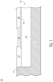
- FIG. 1 illustrates, in a simplified cross-sectional view, a portion of an example semiconductor device 100 having a UBM structure at a stage of manufacture in accordance with an embodiment.
- the semiconductor device 100 includes a semiconductor die 102 partially encapsulated with an encapsulant 112 such as an epoxy molding compound (EMC).
- EMC epoxy molding compound
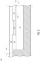
- FIG. 2 illustrates, in a simplified cross-sectional view, the example semiconductor device 100 at a subsequent stage of manufacture in accordance with an embodiment.
- a non-conductive layer 202 is deposited or otherwise formed over the active side of the semiconductor die 102 and the first surface 114 of the encapsulant 112.
- the non-conductive layer 202 may be formed from suitable non-conductive materials such as EMC, Ajinomoto build-up film (ABF), photosensitive dielectric material, and the like.
- FIG. 4A and FIG. 4B illustrate, in simplified plan and cross-sectional views, the example semiconductor device 100 at a subsequent stage of manufacture in accordance with an embodiment.
- FIG. 4A depicts a bottom-side-up plan view 410 of the portion of the semiconductor device 100
- FIG. 4B depicts a cross-sectional view corresponding with FIG. 4A .
- a laser ablated trench 402 is formed in the non-conductive layer 202 proximate to a perimeter of the opening 302 and substantially surrounding (e.g., encircling) the opening.
- the laser ablated trench 402 may be formed having desired cross-sectional depth 404 and width 408 dimensions sufficient for enhancing adhesion between the non-conductive layer 202 and the subsequent UBM. For example, it may be desirable to form the laser ablated trench 402 with a predetermined cross-sectional depth 404 in a range of 25% to 50% of the thickness dimension 406 of the non-conductive layer 202. In this embodiment, a portion of the first surface 204 of the non-conductive layer 202 remains between the inner side wall of the laser ablated trench 402 and the perimeter of the opening 302.
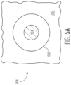
- the laser ablated trench 502 is formed at the first surface 204 of the non-conductive layer 202 in a somewhat similar manner as the laser ablated trench 402.
- the laser ablated trench 502 includes an outer sidewall without an inner sidewall thus having a cross-sectional depth continuous from the outer sidewall through to the opening 302 as depicted in FIG. 5B .
- a larger bottom surface area of the trench results with the substantially roughened texture configured for further improved adhesion between non-conductive layer 202 and the subsequent UBM structure.
- no portion of the first surface 204 of the non-conductive layer 202 remains between the outer sidewall of the laser ablated trench 502 and the opening 302.
- the seed layer 602 may be formed as a relatively thin layer (e.g., ⁇ 0.1-0.5 microns) and may include titanium, tungsten, palladium, copper, or suitable combinations thereof suitable for plating an UBM structure with a conductive material such as copper.
- the seed layer 602 may also serve as a barrier layer to avoid diffusion into the bond pad 104 and enhance adhesion to underlying non-conductive layer 202.
- FIG. 7 illustrates, in a simplified cross-sectional view, the example semiconductor device 100 at a subsequent stage of manufacture in accordance with an embodiment.
- a conductive layer 704 is formed on the seed layer 602 to form the UBM structure 706.
- a plating mask layer 702 is applied on the seed layer 602 and patterned to define predetermined areas to be plated (e.g., UBM structures).
- the semiconductor device 100 is subjected to a plating process.
- the conductive layer 704 includes a copper material and is formed by utilizing the seed layer 402 in a copper plating process.
- the copper plating process may be characterized as an electroless process or an electroplating process.
- the plated conductive layer 704 forms a conformal conductive layer over the exposed bond pad 104 as well as the laser ablated trench 402 of the UBM structure 706.
- the conductive layer 704 may be incorporated a redistribution layer (RDL) of a package substrate.
- RDL redistribution layer
- FIG. 8 illustrates, in a simplified cross-sectional view, the example semiconductor device 100 at a subsequent stage of manufacture in accordance with an embodiment.
- a conductive connector 802 e.g., solder ball
- the conductive connector 802 is placed onto the UBM structure 706 and reflowed.
- a flux material may be applied to the surface of UBM structure 706 before placing the conductive connector 802 onto the UBM structure to improve wetting and adhesion.
- the conductive connector 802 is formed as a solder ball.
- the conductive connector 802 may be in the form of a suitable conductive structure such as a solder bump, gold stud, copper pillar, or the like.
- the method may further include affixing a conductive connector to the UBM structure.
- the method may further include after forming the laser ablated trench, applying a seed layer on the non-conductive layer and the exposed portion of the bond pad.
- the method may further include patterning a mask layer on the seed layer before plating to form the UBM structure.
- the method may further include after plating to form the UBM structure, removing the mask layer and the seed layer portion underlying the mask layer.
- the laser ablated trench may have a depth in a range of 25% to 50% of a thickness of the non-conductive layer.
- the opening may be formed by way of laser ablation at a higher energy level than that of the formation of the laser ablated trench.
- a semiconductor device including a semiconductor die partially encapsulated with an encapsulant, an active side of the semiconductor die exposed and substantially coplanar with a first surface of the encapsulant; a non-conductive layer formed over the active side of the semiconductor die and the first surface of the encapsulant; an opening formed in the non-conductive layer exposing a portion of a bond pad of the semiconductor die; a laser ablated trench formed at a first surface of the non-conductive layer proximate to a perimeter of the opening, a bottom surface of the laser ablated trench substantially roughened; and an under-bump metallization (UBM) structure formed over the bond pad and laser ablated trench.
- UBM under-bump metallization
- the laser ablated trench may be formed at least partially surrounding the perimeter of the opening.
- the substantially roughed bottom of the laser ablated trench may be continuous into the opening.
- the semiconductor device may further include a conductive connector affixed to the UBM structure, the conductive connector configured for connection to a printed circuit board.
- the non-conductive layer may be formed as an Ajinomoto build-up film (ABF).
- the laser ablated trench may have a depth in a range of 25% to 50% of a thickness of the non-conductive layer.
- a method including forming a non-conductive layer over an active side of a semiconductor die and a first surface of an encapsulant, the encapsulant partially encapsulating the semiconductor die; forming a laser ablated opening in the non-conductive layer exposing a portion of a bond pad of the semiconductor die; forming a laser ablated trench at a first surface of the non-conductive layer proximate to a perimeter of the opening, a bottom surface of the laser ablated trench substantially roughened; and plating to form an under-bump metallization (UBM) structure over the bond pad and laser ablated trench.
- UBM under-bump metallization
- the laser ablated trench may be formed at least partially surrounding the perimeter of the laser ablated opening.
- the substantially roughed bottom of the laser ablated trench may be continuous into the laser ablated opening.
- the method may further include affixing a conductive connector to the UBM structure.
- the laser ablated trench may have a depth in a range of 25% to 50% of a thickness of the non-conductive layer.
- the semiconductor device includes a semiconductor die partially encapsulated with an encapsulant. An active side of the semiconductor die is exposed and coplanar with a surface of the encapsulant. A non-conductive layer is formed over an active side of semiconductor die and surface of the encapsulant. An opening in the non-conductive layer is formed to expose a bond pad. A laser ablated trench is formed at the surface of the non-conductive layer near a perimeter of the opening. By using a low energy laser to form the trench, a bottom surface of the trench is roughened.
- the UBM structure is formed by plating over the trench and exposed pad region. The rough texture of the trench allows for superior adhesion of the UBM structure at the trench. By forming the UBM in this manner, potential stress induced delamination is minimized thus improving overall reliability of the semiconductor device.
Landscapes
- Laser Beam Processing (AREA)
- Engineering & Computer Science (AREA)
- Manufacturing & Machinery (AREA)
- Internal Circuitry In Semiconductor Integrated Circuit Devices (AREA)
Abstract
Description
- This disclosure relates generally to semiconductor device packaging, and more specifically, to a semiconductor device with under-bump metallization and method of forming the same.
- Today, there is an increasing trend to include sophisticated semiconductor devices in products and systems that are used every day. These sophisticated semiconductor devices may include features for specific applications which may impact the configuration of the semiconductor device packages, for example. For some features and applications, the configuration of the semiconductor device packages may be susceptible to lower reliability which could impact performance and system costs. Accordingly, significant challenges exist in accommodating these features and applications while minimizing the impact on semiconductor devices' reliability while minimizing impact on performance and costs.
- The present invention is illustrated by way of example and is not limited by the accompanying figures, in which like references indicate similar elements. Elements in the figures are illustrated for simplicity and clarity and have not necessarily been drawn to scale.
-
FIG. 1 through FIG. 3 illustrate, in simplified cross-sectional views, an example semiconductor device at stages of manufacture in accordance with an embodiment. -
FIG. 4A andFIG. 4B illustrate, in simplified plan and corresponding cross-sectional views, the example semiconductor device at a subsequent stage of manufacture in accordance with an embodiment. -
FIG. 5A andFIG. 5B illustrate, in simplified plan and corresponding cross-sectional views, the example semiconductor device at an alternative stage of manufacture in accordance with an embodiment. -
FIG. 6 through FIG. 8 illustrate, in simplified cross-sectional views, the example semiconductor device at subsequent stages of manufacture in accordance with an embodiment. - Generally, there is provided, a semiconductor device with an under-bump metallization (UBM) structure. The semiconductor device includes a semiconductor die partially encapsulated with an encapsulant. An active side of the semiconductor die is exposed and coplanar with a surface of the encapsulant. A non-conductive layer is formed over an active side of semiconductor die and surface of the encapsulant. An opening in the non-conductive layer is formed to expose a bond pad. A laser ablated trench is formed at the surface of the non-conductive layer near a perimeter of the opening. By using a low energy laser to form the trench, a bottom surface of the trench is roughened. The UBM structure is formed by plating over the trench and exposed pad region. The rough texture of the trench allows for superior adhesion of the UBM structure at the trench. By forming the UBM in this manner, potential stress induced delamination is minimized thus improving overall reliability of the semiconductor device.
-
FIG. 1 illustrates, in a simplified cross-sectional view, a portion of anexample semiconductor device 100 having a UBM structure at a stage of manufacture in accordance with an embodiment. At this stage of manufacture, thesemiconductor device 100 includes asemiconductor die 102 partially encapsulated with anencapsulant 112 such as an epoxy molding compound (EMC). Thesemiconductor device 100 portion depicted inFIG. 1 through FIG. 8 at stages of manufacture is shown in a bottom side up orientation. - The
semiconductor die 102 has an active side (e.g., major side having circuitry) and a backside (e.g., major side opposite of the active side). In this embodiment, the active side of thesemiconductor die 102 is exposed (e.g., not encapsulated) and substantially coplanar with afirst surface 114 of theencapsulant 112. The semiconductor die 102 includes a substrate (e.g., bulk)portion 110, a conductive interconnect trace 106 (e.g., copper, aluminum, or other suitable metal), abond pad 104 conductively connected to the trace, and afinal passivation layer 108 formed over the active side of the die. Thebond pad 104 is configured for conductive connection to printed circuit board (PCB) by way of a UBM structure formed at a subsequent stage, for example. The term "conductive," as used herein, generally refers to electrical conductivity unless otherwise noted. - The semiconductor die 102 may be formed from any suitable semiconductor material, such as silicon, germanium, gallium arsenide, gallium nitride, silicon nitride, silicon carbide, and the like. The semiconductor die 102 may further include any digital circuits, analog circuits, RF circuits, memory, signal processor, MEMS, sensors, the like, and combinations thereof. The semiconductor die 102 may include any number of conductive interconnect layers and passivation layers. For illustration purposes, the interconnect
layer forming trace 106 and thefinal passivation layer 108 are depicted. -
FIG. 2 illustrates, in a simplified cross-sectional view, theexample semiconductor device 100 at a subsequent stage of manufacture in accordance with an embodiment. At this stage of manufacture, anon-conductive layer 202 is deposited or otherwise formed over the active side of the semiconductor die 102 and thefirst surface 114 of theencapsulant 112. Thenon-conductive layer 202 may be formed from suitable non-conductive materials such as EMC, Ajinomoto build-up film (ABF), photosensitive dielectric material, and the like. -
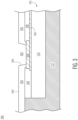
FIG. 3 illustrates, in a simplified cross-sectional view, theexample semiconductor device 100 at a subsequent stage of manufacture in accordance with an embodiment. At this stage of manufacture, anopening 302 is formed in thenon-conductive layer 202. Theopening 302 is formed through thenon-conductive layer 202 and located over thebond pad 104 such that a substantial portion of a top surface of thebond pad 104 is exposed.Sidewalls 304 of the opening 302 surround the exposed portion of thebond pad 104 and form a perimeter of the opening. In this embodiment, theopening 302 is formed by way of high energy laser ablation. By forming theopening 302 in this manner, sidewalls of the opening may result with a rough texture thus providing improved adhesion with the UBM structure formed at a subsequent stage, for example. In some embodiments, the opening 302 may be formed by using known mask patterning and wet or dry chemical etch process methods. -
FIG. 4A andFIG. 4B illustrate, in simplified plan and cross-sectional views, theexample semiconductor device 100 at a subsequent stage of manufacture in accordance with an embodiment. For example,FIG. 4A depicts a bottom-side-upplan view 410 of the portion of thesemiconductor device 100 andFIG. 4B depicts a cross-sectional view corresponding withFIG. 4A . At this stage, a laser ablatedtrench 402 is formed in thenon-conductive layer 202 proximate to a perimeter of theopening 302 and substantially surrounding (e.g., encircling) the opening. - In this embodiment, the laser ablated
trench 402 is formed at a first (e.g., outermost)surface 204 of thenon-conductive layer 202. The laser ablatedtrench 402 is configured to enhance adhesion between thenon-conductive layer 202 and the UBM structure formed at a subsequent stage, for example. The laser ablatedtrench 402 may be formed by way of a low energy laser, for example, configured to remove material at thefirst surface 204 of thenon-conductive layer 202. By forming the laser ablatedtrench 402 in this manner, a bottom surface of the trench may result with a substantially roughened texture configured for improved adhesion. The laser ablatedtrench 402 may be formed having desiredcross-sectional depth 404 andwidth 408 dimensions sufficient for enhancing adhesion between thenon-conductive layer 202 and the subsequent UBM. For example, it may be desirable to form the laser ablatedtrench 402 with a predeterminedcross-sectional depth 404 in a range of 25% to 50% of thethickness dimension 406 of the non-conductivelayer 202. In this embodiment, a portion of thefirst surface 204 of thenon-conductive layer 202 remains between the inner side wall of the laser ablatedtrench 402 and the perimeter of theopening 302. -
FIG. 5A andFIG. 5B illustrate, in simplified plan and cross-sectional views, theexample semiconductor device 100 at an alternate stage of manufacture in accordance with an embodiment. For example,FIG. 5A depicts a bottom-side-upplan view 504 of the portion of thesemiconductor device 100 andFIG. 5B depicts a cross-sectional view corresponding withFIG. 5A . At this stage, a laser ablatedtrench 502 is formed in thenon-conductive layer 202 extending into theopening 302 and substantially surrounding (e.g., encircling) the opening. The laser ablatedtrench 502 depicted inFIG. 5A andFIG. 5B is an alternative to the laser ablatedtrench 402 depicted inFIG. 4A andFIG. 4B . - In this embodiment, the laser ablated
trench 502 is formed at thefirst surface 204 of thenon-conductive layer 202 in a somewhat similar manner as the laser ablatedtrench 402. However, the laser ablatedtrench 502 includes an outer sidewall without an inner sidewall thus having a cross-sectional depth continuous from the outer sidewall through to theopening 302 as depicted inFIG. 5B . By forming the laser ablatedtrench 502 in this manner, a larger bottom surface area of the trench results with the substantially roughened texture configured for further improved adhesion betweennon-conductive layer 202 and the subsequent UBM structure. In this embodiment, no portion of thefirst surface 204 of thenon-conductive layer 202 remains between the outer sidewall of the laser ablatedtrench 502 and theopening 302. -
FIG. 6 illustrates, in a simplified cross-sectional view, theexample semiconductor device 100 at a subsequent stage of manufacture in accordance with an embodiment. At this stage of manufacture, aseed layer 602 is formed over thenon-conductive layer 202 and exposedbond pad 104 to expose a portion of the surface of the bond pad. In this embodiment, theseed layer 602 is sputtered, deposited, or otherwise applied on thefirst surface 204 of thenon-conductive layer 202, the sidewalls and bottom surface of the laser ablatedtrench 402, the sidewalls of theopening 302, and the exposed surface of thebond pad 104. Theseed layer 602 may be formed as a relatively thin layer (e.g., ~0.1-0.5 microns) and may include titanium, tungsten, palladium, copper, or suitable combinations thereof suitable for plating an UBM structure with a conductive material such as copper. Theseed layer 602 may also serve as a barrier layer to avoid diffusion into thebond pad 104 and enhance adhesion to underlyingnon-conductive layer 202. -
FIG. 7 illustrates, in a simplified cross-sectional view, theexample semiconductor device 100 at a subsequent stage of manufacture in accordance with an embodiment. At this stage of manufacture, aconductive layer 704 is formed on theseed layer 602 to form theUBM structure 706. In this embodiment, aplating mask layer 702 is applied on theseed layer 602 and patterned to define predetermined areas to be plated (e.g., UBM structures). After theplating mask layer 702 is patterned, thesemiconductor device 100 is subjected to a plating process. In this embodiment, theconductive layer 704 includes a copper material and is formed by utilizing theseed layer 402 in a copper plating process. The copper plating process may be characterized as an electroless process or an electroplating process. The platedconductive layer 704 forms a conformal conductive layer over the exposedbond pad 104 as well as the laser ablatedtrench 402 of theUBM structure 706. In some embodiments, theconductive layer 704 may be incorporated a redistribution layer (RDL) of a package substrate. -
FIG. 8 illustrates, in a simplified cross-sectional view, theexample semiconductor device 100 at a subsequent stage of manufacture in accordance with an embodiment. At this stage of manufacture, a conductive connector 802 (e.g., solder ball) is attached to theUBM structure 706. Theconductive connector 802 is placed onto theUBM structure 706 and reflowed. A flux material may be applied to the surface ofUBM structure 706 before placing theconductive connector 802 onto the UBM structure to improve wetting and adhesion. In this embodiment, theconductive connector 802 is formed as a solder ball. In other embodiments, theconductive connector 802 may be in the form of a suitable conductive structure such as a solder bump, gold stud, copper pillar, or the like. After attaching theconductive connector 802 to theUBM structure 706, an anti-tarnish or preservative material may be applied over exposed portions of theconductive layer 704. The anti-tarnish or preservative material may bond with theconductive layer 704 in a manner that protects exposed surfaces of theconductive layer 704 from oxidation or corrosion, for example. - In one embodiment, there is provided, a method including forming a non-conductive layer over an active side of a semiconductor die, the semiconductor die partially encapsulated with an encapsulant; forming an opening in the non-conductive layer, the opening exposing a portion of a bond pad of the semiconductor die; forming a laser ablated trench at a first surface of the non-conductive layer proximate to a perimeter of the opening, a bottom surface of the laser ablated trench substantially roughened; and plating to form an under-bump metallization (UBM) structure over the bond pad and laser ablated trench. The laser ablated trench may be formed at least partially surrounding the perimeter of the opening. The substantially roughed bottom of the laser ablated trench may be continuous into the opening. The method may further include affixing a conductive connector to the UBM structure. The method may further include after forming the laser ablated trench, applying a seed layer on the non-conductive layer and the exposed portion of the bond pad. The method may further include patterning a mask layer on the seed layer before plating to form the UBM structure. The method may further include after plating to form the UBM structure, removing the mask layer and the seed layer portion underlying the mask layer. The laser ablated trench may have a depth in a range of 25% to 50% of a thickness of the non-conductive layer. The opening may be formed by way of laser ablation at a higher energy level than that of the formation of the laser ablated trench.
- In another embodiment, there is provided, a semiconductor device including a semiconductor die partially encapsulated with an encapsulant, an active side of the semiconductor die exposed and substantially coplanar with a first surface of the encapsulant; a non-conductive layer formed over the active side of the semiconductor die and the first surface of the encapsulant; an opening formed in the non-conductive layer exposing a portion of a bond pad of the semiconductor die; a laser ablated trench formed at a first surface of the non-conductive layer proximate to a perimeter of the opening, a bottom surface of the laser ablated trench substantially roughened; and an under-bump metallization (UBM) structure formed over the bond pad and laser ablated trench. The laser ablated trench may be formed at least partially surrounding the perimeter of the opening. The substantially roughed bottom of the laser ablated trench may be continuous into the opening. The semiconductor device may further include a conductive connector affixed to the UBM structure, the conductive connector configured for connection to a printed circuit board. The non-conductive layer may be formed as an Ajinomoto build-up film (ABF). The laser ablated trench may have a depth in a range of 25% to 50% of a thickness of the non-conductive layer.
- In yet another embodiment, there is provided, a method including forming a non-conductive layer over an active side of a semiconductor die and a first surface of an encapsulant, the encapsulant partially encapsulating the semiconductor die; forming a laser ablated opening in the non-conductive layer exposing a portion of a bond pad of the semiconductor die; forming a laser ablated trench at a first surface of the non-conductive layer proximate to a perimeter of the opening, a bottom surface of the laser ablated trench substantially roughened; and plating to form an under-bump metallization (UBM) structure over the bond pad and laser ablated trench. The laser ablated trench may be formed at least partially surrounding the perimeter of the laser ablated opening. The substantially roughed bottom of the laser ablated trench may be continuous into the laser ablated opening. The method may further include affixing a conductive connector to the UBM structure. The laser ablated trench may have a depth in a range of 25% to 50% of a thickness of the non-conductive layer.
- By now, it should be appreciated that there has been provided a semiconductor device with an under-bump metallization (UBM) structure. The semiconductor device includes a semiconductor die partially encapsulated with an encapsulant. An active side of the semiconductor die is exposed and coplanar with a surface of the encapsulant. A non-conductive layer is formed over an active side of semiconductor die and surface of the encapsulant. An opening in the non-conductive layer is formed to expose a bond pad. A laser ablated trench is formed at the surface of the non-conductive layer near a perimeter of the opening. By using a low energy laser to form the trench, a bottom surface of the trench is roughened. The UBM structure is formed by plating over the trench and exposed pad region. The rough texture of the trench allows for superior adhesion of the UBM structure at the trench. By forming the UBM in this manner, potential stress induced delamination is minimized thus improving overall reliability of the semiconductor device.
- The terms "front," "back," "top," "bottom," "over," "under" and the like in the description and in the claims, if any, are used for descriptive purposes and not necessarily for describing permanent relative positions. It is understood that the terms so used are interchangeable under appropriate circumstances such that the embodiments of the invention described herein are, for example, capable of operation in other orientations than those illustrated or otherwise described herein.
- Although the invention is described herein with reference to specific embodiments, various modifications and changes can be made without departing from the scope of the present invention as set forth in the claims below. Accordingly, the specification and figures are to be regarded in an illustrative rather than a restrictive sense, and all such modifications are intended to be included within the scope of the present invention. Any benefits, advantages, or solutions to problems that are described herein with regard to specific embodiments are not intended to be construed as a critical, required, or essential feature or element of any or all the claims.
- Furthermore, the terms "a" or "an," as used herein, are defined as one or more than one. Also, the use of introductory phrases such as "at least one" and "one or more" in the claims should not be construed to imply that the introduction of another claim element by the indefinite articles "a" or "an" limits any particular claim containing such introduced claim element to inventions containing only one such element, even when the same claim includes the introductory phrases "one or more" or "at least one" and indefinite articles such as "a" or "an." The same holds true for the use of definite articles.
- Unless stated otherwise, terms such as "first" and "second" are used to arbitrarily distinguish between the elements such terms describe. Thus, these terms are not necessarily intended to indicate temporal or other prioritization of such elements.
Claims (15)
- A method comprising:forming a non-conductive layer over an active side of a semiconductor die, the semiconductor die partially encapsulated with an encapsulant;forming an opening in the non-conductive layer, the opening exposing a portion of a bond pad of the semiconductor die;forming a laser ablated trench at a first surface of the non-conductive layer proximate to a perimeter of the opening, a bottom surface of the laser ablated trench substantially roughened; andplating to form an under-bump metallization, UBM, structure over the bond pad and laser ablated trench.
- The method of claim 1, wherein the laser ablated trench is formed at least partially surrounding the perimeter of the opening.
- The method of claim 1 or 2, wherein the substantially roughed bottom of the laser ablated trench is continuous into the opening.
- The method of any preceding claim, further comprising affixing a conductive connector to the UBM structure.
- The method of any preceding claim, further comprising after forming the laser ablated trench, applying a seed layer on the non-conductive layer and the exposed portion of the bond pad.
- The method of claim 5, further comprising patterning a mask layer on the seed layer before plating to form the UBM structure.
- The method of claim 6, further comprising after plating to form the UBM structure, removing the mask layer and the seed layer portion underlying the mask layer.
- The method of any preceding claim, wherein the laser ablated trench has a depth in a range of 25% to 50% of a thickness of the non-conductive layer.
- The method of any preceding claim, wherein the opening is formed by way of laser ablation at a higher energy level than that of the formation of the laser ablated trench.
- A semiconductor device comprising:a semiconductor die partially encapsulated with an encapsulant, an active side of the semiconductor die exposed and substantially coplanar with a first surface of the encapsulant;a non-conductive layer formed over the active side of the semiconductor die and the first surface of the encapsulant;an opening formed in the non-conductive layer exposing a portion of a bond pad of the semiconductor die;a laser ablated trench formed at a first surface of the non-conductive layer proximate to a perimeter of the opening, a bottom surface of the laser ablated trench substantially roughened; andan under-bump metallization, UBM, structure formed over the bond pad and laser ablated trench.
- The semiconductor device of claim 10, wherein the laser ablated trench is formed at least partially surrounding the perimeter of the opening.
- The semiconductor device of claim 10 or 11, wherein the substantially roughed bottom of the laser ablated trench is continuous into the opening.
- The semiconductor device of any of claims 10 to 12, further comprising a conductive connector affixed to the UBM structure, the conductive connector configured for connection to a printed circuit board.
- The semiconductor device of any of claims 10 to 13, wherein the non-conductive layer is formed as an Ajinomoto build-up film, ABF.
- The semiconductor device of any of claims 10 to 14, wherein the laser ablated trench has a depth in a range of 25% to 50% of a thickness of the non-conductive layer.
Applications Claiming Priority (1)
| Application Number | Priority Date | Filing Date | Title |
|---|---|---|---|
| US17/811,132 US20240014152A1 (en) | 2022-07-07 | 2022-07-07 | Semiconductor device with under-bump metallization and method therefor |
Publications (2)
| Publication Number | Publication Date |
|---|---|
| EP4303912A1 true EP4303912A1 (en) | 2024-01-10 |
| EP4303912B1 EP4303912B1 (en) | 2025-03-12 |
Family
ID=87047706
Family Applications (1)
| Application Number | Title | Priority Date | Filing Date |
|---|---|---|---|
| EP23181527.5A Active EP4303912B1 (en) | 2022-07-07 | 2023-06-26 | Semiconductor device with under-bump metallization and method therefor |
Country Status (2)
| Country | Link |
|---|---|
| US (1) | US20240014152A1 (en) |
| EP (1) | EP4303912B1 (en) |
Families Citing this family (1)
| Publication number | Priority date | Publication date | Assignee | Title |
|---|---|---|---|---|
| US12512440B2 (en) * | 2022-09-18 | 2025-12-30 | Taiwan Semiconductor Manufacturing Company, Ltd. | Semiconductor structure, stacked structure with terminal comprising capping layer and manufacturing method thereof |
Citations (1)
| Publication number | Priority date | Publication date | Assignee | Title |
|---|---|---|---|---|
| US20140264839A1 (en) * | 2013-03-15 | 2014-09-18 | Taiwan Semiconductor Manufacturing Company, Ltd. | Packaged Semiconductor Devices, Methods of Packaging Semiconductor Devices, and PoP Devices |
Family Cites Families (14)
| Publication number | Priority date | Publication date | Assignee | Title |
|---|---|---|---|---|
| JP3860000B2 (en) * | 2001-09-07 | 2006-12-20 | Necエレクトロニクス株式会社 | Semiconductor device and manufacturing method thereof |
| JP5143382B2 (en) * | 2006-07-27 | 2013-02-13 | オンセミコンダクター・トレーディング・リミテッド | Semiconductor device and manufacturing method thereof |
| US7470985B2 (en) * | 2006-07-31 | 2008-12-30 | International Business Machines Corporation | Solder connector structure and method |
| JP2009182272A (en) * | 2008-01-31 | 2009-08-13 | Sanyo Electric Co Ltd | Device mounting substrate and manufacturing method thereof, semiconductor module and manufacturing method thereof, and portable device |
| US20110266670A1 (en) * | 2010-04-30 | 2011-11-03 | Luke England | Wafer level chip scale package with annular reinforcement structure |
| US8610274B2 (en) * | 2010-09-14 | 2013-12-17 | Infineon Technologies Ag | Die structure, die arrangement and method of processing a die |
| KR101718011B1 (en) * | 2010-11-01 | 2017-03-21 | 삼성전자주식회사 | Semiconductor packages and methods for the same |
| US9570410B1 (en) * | 2015-07-31 | 2017-02-14 | Taiwan Semiconductor Manufacturing Company, Ltd. | Methods of forming connector pad structures, interconnect structures, and structures thereof |
| JP6628031B2 (en) * | 2015-11-04 | 2020-01-08 | ローム株式会社 | Electronic components |
| TWI596734B (en) * | 2016-06-07 | 2017-08-21 | 南茂科技股份有限公司 | Semiconductor device |
| KR102658923B1 (en) * | 2016-09-12 | 2024-04-18 | 삼성전자주식회사 | Semiconductor device and semiconductor package |
| JP6663400B2 (en) * | 2017-09-11 | 2020-03-11 | 株式会社Kokusai Electric | Semiconductor device manufacturing method, substrate processing apparatus, and program |
| KR102855117B1 (en) * | 2021-06-03 | 2025-09-05 | 삼성디스플레이 주식회사 | Display device and method of manufacturing the same |
| JP7693487B2 (en) * | 2021-09-22 | 2025-06-17 | ローム株式会社 | Semiconductor device and method for manufacturing the same |
-
2022
- 2022-07-07 US US17/811,132 patent/US20240014152A1/en active Pending
-
2023
- 2023-06-26 EP EP23181527.5A patent/EP4303912B1/en active Active
Patent Citations (1)
| Publication number | Priority date | Publication date | Assignee | Title |
|---|---|---|---|---|
| US20140264839A1 (en) * | 2013-03-15 | 2014-09-18 | Taiwan Semiconductor Manufacturing Company, Ltd. | Packaged Semiconductor Devices, Methods of Packaging Semiconductor Devices, and PoP Devices |
Also Published As
| Publication number | Publication date |
|---|---|
| EP4303912B1 (en) | 2025-03-12 |
| US20240014152A1 (en) | 2024-01-11 |
Similar Documents
| Publication | Publication Date | Title |
|---|---|---|
| US9165898B2 (en) | Method of manufacturing semiconductor device with through hole | |
| KR100658543B1 (en) | Semiconductor device and manufacturing method thereof | |
| US6876061B2 (en) | Chip scale surface mount package for semiconductor device and process of fabricating the same | |
| US7964450B2 (en) | Wirebondless wafer level package with plated bumps and interconnects | |
| KR100563887B1 (en) | Semiconductor device and manufacturing method thereof | |
| US7589396B2 (en) | Chip scale surface mount package for semiconductor device and process of fabricating the same | |
| KR100714253B1 (en) | Method of manufacturing semiconductor device | |
| KR20060041997A (en) | Semiconductor device and manufacturing method thereof | |
| KR20040101924A (en) | Semiconductor device and method for manufacturing the same | |
| EP1686622A2 (en) | Semiconductor device and manufacturing method of the same | |
| US20080075841A1 (en) | Apparatus and method incorporating discrete passive components in an electronic package | |
| EP4303912B1 (en) | Semiconductor device with under-bump metallization and method therefor | |
| EP4345893A1 (en) | Semiconductor device with redistribution metallization and method therefor | |
| US20230307402A1 (en) | Semiconductor device under bump structure and method therefor | |
| TW202514960A (en) | Electronic devices and methods of manufacturing electronic devices | |
| US20230275050A1 (en) | Silver- and gold-plated conductive members | |
| US12588518B2 (en) | Semiconductor device with reinforced dielectric and method therefor | |
| EP4468343A1 (en) | Semiconductor device having wired under bump structure and method therefor | |
| US20240203919A1 (en) | Integrated circuit having exposed leads | |
| US12322719B2 (en) | Semiconductor device structure and method therefor | |
| US20090324906A1 (en) | Semiconductor with top-side wrap-around flange contact | |
| CN119742284A (en) | Semiconductor package with insulating layer |
Legal Events
| Date | Code | Title | Description |
|---|---|---|---|
| PUAI | Public reference made under article 153(3) epc to a published international application that has entered the european phase |
Free format text: ORIGINAL CODE: 0009012 |
|
| STAA | Information on the status of an ep patent application or granted ep patent |
Free format text: STATUS: THE APPLICATION HAS BEEN PUBLISHED |
|
| AK | Designated contracting states |
Kind code of ref document: A1 Designated state(s): AL AT BE BG CH CY CZ DE DK EE ES FI FR GB GR HR HU IE IS IT LI LT LU LV MC ME MK MT NL NO PL PT RO RS SE SI SK SM TR |
|
| STAA | Information on the status of an ep patent application or granted ep patent |
Free format text: STATUS: REQUEST FOR EXAMINATION WAS MADE |
|
| 17P | Request for examination filed |
Effective date: 20240710 |
|
| RBV | Designated contracting states (corrected) |
Designated state(s): AL AT BE BG CH CY CZ DE DK EE ES FI FR GB GR HR HU IE IS IT LI LT LU LV MC ME MK MT NL NO PL PT RO RS SE SI SK SM TR |
|
| GRAP | Despatch of communication of intention to grant a patent |
Free format text: ORIGINAL CODE: EPIDOSNIGR1 |
|
| STAA | Information on the status of an ep patent application or granted ep patent |
Free format text: STATUS: GRANT OF PATENT IS INTENDED |
|
| RIC1 | Information provided on ipc code assigned before grant |
Ipc: H01L 23/31 20060101ALN20241125BHEP Ipc: H01L 23/48 20060101ALI20241125BHEP Ipc: H01L 21/60 20060101AFI20241125BHEP |
|
| INTG | Intention to grant announced |
Effective date: 20241217 |
|
| GRAS | Grant fee paid |
Free format text: ORIGINAL CODE: EPIDOSNIGR3 |
|
| GRAL | Information related to payment of fee for publishing/printing deleted |
Free format text: ORIGINAL CODE: EPIDOSDIGR3 |
|
| GRAS | Grant fee paid |
Free format text: ORIGINAL CODE: EPIDOSNIGR3 |
|
| GRAA | (expected) grant |
Free format text: ORIGINAL CODE: 0009210 |
|
| STAA | Information on the status of an ep patent application or granted ep patent |
Free format text: STATUS: THE PATENT HAS BEEN GRANTED |
|
| AK | Designated contracting states |
Kind code of ref document: B1 Designated state(s): AL AT BE BG CH CY CZ DE DK EE ES FI FR GB GR HR HU IE IS IT LI LT LU LV MC ME MK MT NL NO PL PT RO RS SE SI SK SM TR |
|
| REG | Reference to a national code |
Ref country code: GB Ref legal event code: FG4D |
|
| REG | Reference to a national code |
Ref country code: CH Ref legal event code: EP |
|
| REG | Reference to a national code |
Ref country code: DE Ref legal event code: R096 Ref document number: 602023002371 Country of ref document: DE |
|
| REG | Reference to a national code |
Ref country code: IE Ref legal event code: FG4D |
|
| PG25 | Lapsed in a contracting state [announced via postgrant information from national office to epo] |
Ref country code: RS Free format text: LAPSE BECAUSE OF FAILURE TO SUBMIT A TRANSLATION OF THE DESCRIPTION OR TO PAY THE FEE WITHIN THE PRESCRIBED TIME-LIMIT Effective date: 20250612 |
|
| PG25 | Lapsed in a contracting state [announced via postgrant information from national office to epo] |
Ref country code: FI Free format text: LAPSE BECAUSE OF FAILURE TO SUBMIT A TRANSLATION OF THE DESCRIPTION OR TO PAY THE FEE WITHIN THE PRESCRIBED TIME-LIMIT Effective date: 20250312 |
|
| PGFP | Annual fee paid to national office [announced via postgrant information from national office to epo] |
Ref country code: DE Payment date: 20250520 Year of fee payment: 3 |
|
| PG25 | Lapsed in a contracting state [announced via postgrant information from national office to epo] |
Ref country code: ES Free format text: LAPSE BECAUSE OF FAILURE TO SUBMIT A TRANSLATION OF THE DESCRIPTION OR TO PAY THE FEE WITHIN THE PRESCRIBED TIME-LIMIT Effective date: 20250312 |
|
| REG | Reference to a national code |
Ref country code: LT Ref legal event code: MG9D |
|
| PG25 | Lapsed in a contracting state [announced via postgrant information from national office to epo] |
Ref country code: NO Free format text: LAPSE BECAUSE OF FAILURE TO SUBMIT A TRANSLATION OF THE DESCRIPTION OR TO PAY THE FEE WITHIN THE PRESCRIBED TIME-LIMIT Effective date: 20250612 |
|
| PG25 | Lapsed in a contracting state [announced via postgrant information from national office to epo] |
Ref country code: HR Free format text: LAPSE BECAUSE OF FAILURE TO SUBMIT A TRANSLATION OF THE DESCRIPTION OR TO PAY THE FEE WITHIN THE PRESCRIBED TIME-LIMIT Effective date: 20250312 |
|
| REG | Reference to a national code |
Ref country code: NL Ref legal event code: MP Effective date: 20250312 |
|
| PG25 | Lapsed in a contracting state [announced via postgrant information from national office to epo] |
Ref country code: LV Free format text: LAPSE BECAUSE OF FAILURE TO SUBMIT A TRANSLATION OF THE DESCRIPTION OR TO PAY THE FEE WITHIN THE PRESCRIBED TIME-LIMIT Effective date: 20250312 |
|
| PG25 | Lapsed in a contracting state [announced via postgrant information from national office to epo] |
Ref country code: GR Free format text: LAPSE BECAUSE OF FAILURE TO SUBMIT A TRANSLATION OF THE DESCRIPTION OR TO PAY THE FEE WITHIN THE PRESCRIBED TIME-LIMIT Effective date: 20250613 Ref country code: BG Free format text: LAPSE BECAUSE OF FAILURE TO SUBMIT A TRANSLATION OF THE DESCRIPTION OR TO PAY THE FEE WITHIN THE PRESCRIBED TIME-LIMIT Effective date: 20250312 |
|
| REG | Reference to a national code |
Ref country code: AT Ref legal event code: MK05 Ref document number: 1775768 Country of ref document: AT Kind code of ref document: T Effective date: 20250312 |
|
| PG25 | Lapsed in a contracting state [announced via postgrant information from national office to epo] |
Ref country code: NL Free format text: LAPSE BECAUSE OF FAILURE TO SUBMIT A TRANSLATION OF THE DESCRIPTION OR TO PAY THE FEE WITHIN THE PRESCRIBED TIME-LIMIT Effective date: 20250312 |
|
| PG25 | Lapsed in a contracting state [announced via postgrant information from national office to epo] |
Ref country code: SE Free format text: LAPSE BECAUSE OF FAILURE TO SUBMIT A TRANSLATION OF THE DESCRIPTION OR TO PAY THE FEE WITHIN THE PRESCRIBED TIME-LIMIT Effective date: 20250312 |
|
| PG25 | Lapsed in a contracting state [announced via postgrant information from national office to epo] |
Ref country code: SM Free format text: LAPSE BECAUSE OF FAILURE TO SUBMIT A TRANSLATION OF THE DESCRIPTION OR TO PAY THE FEE WITHIN THE PRESCRIBED TIME-LIMIT Effective date: 20250312 |
|
| PG25 | Lapsed in a contracting state [announced via postgrant information from national office to epo] |
Ref country code: PT Free format text: LAPSE BECAUSE OF FAILURE TO SUBMIT A TRANSLATION OF THE DESCRIPTION OR TO PAY THE FEE WITHIN THE PRESCRIBED TIME-LIMIT Effective date: 20250714 |
|
| PG25 | Lapsed in a contracting state [announced via postgrant information from national office to epo] |
Ref country code: IT Free format text: LAPSE BECAUSE OF FAILURE TO SUBMIT A TRANSLATION OF THE DESCRIPTION OR TO PAY THE FEE WITHIN THE PRESCRIBED TIME-LIMIT Effective date: 20250312 Ref country code: PL Free format text: LAPSE BECAUSE OF FAILURE TO SUBMIT A TRANSLATION OF THE DESCRIPTION OR TO PAY THE FEE WITHIN THE PRESCRIBED TIME-LIMIT Effective date: 20250312 |
|
| PG25 | Lapsed in a contracting state [announced via postgrant information from national office to epo] |
Ref country code: AT Free format text: LAPSE BECAUSE OF FAILURE TO SUBMIT A TRANSLATION OF THE DESCRIPTION OR TO PAY THE FEE WITHIN THE PRESCRIBED TIME-LIMIT Effective date: 20250312 |
|
| PG25 | Lapsed in a contracting state [announced via postgrant information from national office to epo] |
Ref country code: CZ Free format text: LAPSE BECAUSE OF FAILURE TO SUBMIT A TRANSLATION OF THE DESCRIPTION OR TO PAY THE FEE WITHIN THE PRESCRIBED TIME-LIMIT Effective date: 20250312 Ref country code: EE Free format text: LAPSE BECAUSE OF FAILURE TO SUBMIT A TRANSLATION OF THE DESCRIPTION OR TO PAY THE FEE WITHIN THE PRESCRIBED TIME-LIMIT Effective date: 20250312 |
|
| PG25 | Lapsed in a contracting state [announced via postgrant information from national office to epo] |
Ref country code: RO Free format text: LAPSE BECAUSE OF FAILURE TO SUBMIT A TRANSLATION OF THE DESCRIPTION OR TO PAY THE FEE WITHIN THE PRESCRIBED TIME-LIMIT Effective date: 20250312 |
|
| PG25 | Lapsed in a contracting state [announced via postgrant information from national office to epo] |
Ref country code: SK Free format text: LAPSE BECAUSE OF FAILURE TO SUBMIT A TRANSLATION OF THE DESCRIPTION OR TO PAY THE FEE WITHIN THE PRESCRIBED TIME-LIMIT Effective date: 20250312 |
|
| PG25 | Lapsed in a contracting state [announced via postgrant information from national office to epo] |
Ref country code: IS Free format text: LAPSE BECAUSE OF FAILURE TO SUBMIT A TRANSLATION OF THE DESCRIPTION OR TO PAY THE FEE WITHIN THE PRESCRIBED TIME-LIMIT Effective date: 20250712 |
|
| REG | Reference to a national code |
Ref country code: DE Ref legal event code: R079 Ref document number: 602023002371 Country of ref document: DE Free format text: PREVIOUS MAIN CLASS: H01L0021600000 Ipc: H10W0070010000 |
|
| REG | Reference to a national code |
Ref country code: DE Ref legal event code: R097 Ref document number: 602023002371 Country of ref document: DE |
|
| PG25 | Lapsed in a contracting state [announced via postgrant information from national office to epo] |
Ref country code: DK Free format text: LAPSE BECAUSE OF FAILURE TO SUBMIT A TRANSLATION OF THE DESCRIPTION OR TO PAY THE FEE WITHIN THE PRESCRIBED TIME-LIMIT Effective date: 20250312 |
|
| PLBE | No opposition filed within time limit |
Free format text: ORIGINAL CODE: 0009261 |
|
| STAA | Information on the status of an ep patent application or granted ep patent |
Free format text: STATUS: NO OPPOSITION FILED WITHIN TIME LIMIT |
|
| REG | Reference to a national code |
Ref country code: CH Ref legal event code: L10 Free format text: ST27 STATUS EVENT CODE: U-0-0-L10-L00 (AS PROVIDED BY THE NATIONAL OFFICE) Effective date: 20260121 |
|
| PG25 | Lapsed in a contracting state [announced via postgrant information from national office to epo] |
Ref country code: MC Free format text: LAPSE BECAUSE OF FAILURE TO SUBMIT A TRANSLATION OF THE DESCRIPTION OR TO PAY THE FEE WITHIN THE PRESCRIBED TIME-LIMIT Effective date: 20250312 |
|
| PG25 | Lapsed in a contracting state [announced via postgrant information from national office to epo] |
Ref country code: LU Free format text: LAPSE BECAUSE OF NON-PAYMENT OF DUE FEES Effective date: 20250626 |
|
| 26N | No opposition filed |
Effective date: 20251215 |
|
| REG | Reference to a national code |
Ref country code: BE Ref legal event code: MM Effective date: 20250630 |
|
| PG25 | Lapsed in a contracting state [announced via postgrant information from national office to epo] |
Ref country code: IE Free format text: LAPSE BECAUSE OF NON-PAYMENT OF DUE FEES Effective date: 20250626 |
|
| PG25 | Lapsed in a contracting state [announced via postgrant information from national office to epo] |
Ref country code: BE Free format text: LAPSE BECAUSE OF NON-PAYMENT OF DUE FEES Effective date: 20250630 |
|
| PG25 | Lapsed in a contracting state [announced via postgrant information from national office to epo] |
Ref country code: FR Free format text: LAPSE BECAUSE OF NON-PAYMENT OF DUE FEES Effective date: 20250630 |