EP4303689A1 - An electronic system using a power regulator with reduced inrush current - Google Patents
An electronic system using a power regulator with reduced inrush current Download PDFInfo
- Publication number
- EP4303689A1 EP4303689A1 EP23177357.3A EP23177357A EP4303689A1 EP 4303689 A1 EP4303689 A1 EP 4303689A1 EP 23177357 A EP23177357 A EP 23177357A EP 4303689 A1 EP4303689 A1 EP 4303689A1
- Authority
- EP
- European Patent Office
- Prior art keywords
- power
- capacitor
- mode
- regulator
- power regulator
- Prior art date
- Legal status (The legal status is an assumption and is not a legal conclusion. Google has not performed a legal analysis and makes no representation as to the accuracy of the status listed.)
- Pending
Links
Images

Classifications
-
- G—PHYSICS
- G05—CONTROLLING; REGULATING
- G05F—SYSTEMS FOR REGULATING ELECTRIC OR MAGNETIC VARIABLES
- G05F1/00—Automatic systems in which deviations of an electric quantity from one or more predetermined values are detected at the output of the system and fed back to a device within the system to restore the detected quantity to its predetermined value or values, i.e. retroactive systems
- G05F1/10—Regulating voltage or current
- G05F1/46—Regulating voltage or current wherein the variable actually regulated by the final control device is DC
- G05F1/56—Regulating voltage or current wherein the variable actually regulated by the final control device is DC using semiconductor devices in series with the load as final control devices
- G05F1/575—Regulating voltage or current wherein the variable actually regulated by the final control device is DC using semiconductor devices in series with the load as final control devices characterised by the feedback circuit
-
- G—PHYSICS
- G05—CONTROLLING; REGULATING
- G05F—SYSTEMS FOR REGULATING ELECTRIC OR MAGNETIC VARIABLES
- G05F1/00—Automatic systems in which deviations of an electric quantity from one or more predetermined values are detected at the output of the system and fed back to a device within the system to restore the detected quantity to its predetermined value or values, i.e. retroactive systems
- G05F1/10—Regulating voltage or current
- G05F1/46—Regulating voltage or current wherein the variable actually regulated by the final control device is DC
- G05F1/468—Regulating voltage or current wherein the variable actually regulated by the final control device is DC characterised by reference voltage circuitry, e.g. soft start, remote shutdown
-
- G—PHYSICS
- G05—CONTROLLING; REGULATING
- G05F—SYSTEMS FOR REGULATING ELECTRIC OR MAGNETIC VARIABLES
- G05F1/00—Automatic systems in which deviations of an electric quantity from one or more predetermined values are detected at the output of the system and fed back to a device within the system to restore the detected quantity to its predetermined value or values, i.e. retroactive systems
- G05F1/10—Regulating voltage or current
- G05F1/46—Regulating voltage or current wherein the variable actually regulated by the final control device is DC
- G05F1/56—Regulating voltage or current wherein the variable actually regulated by the final control device is DC using semiconductor devices in series with the load as final control devices
- G05F1/565—Regulating voltage or current wherein the variable actually regulated by the final control device is DC using semiconductor devices in series with the load as final control devices sensing a condition of the system or its load in addition to means responsive to deviations in the output of the system, e.g. current, voltage, power factor
-
- G—PHYSICS
- G05—CONTROLLING; REGULATING
- G05F—SYSTEMS FOR REGULATING ELECTRIC OR MAGNETIC VARIABLES
- G05F1/00—Automatic systems in which deviations of an electric quantity from one or more predetermined values are detected at the output of the system and fed back to a device within the system to restore the detected quantity to its predetermined value or values, i.e. retroactive systems
- G05F1/10—Regulating voltage or current
- G05F1/46—Regulating voltage or current wherein the variable actually regulated by the final control device is DC
- G05F1/56—Regulating voltage or current wherein the variable actually regulated by the final control device is DC using semiconductor devices in series with the load as final control devices
- G05F1/565—Regulating voltage or current wherein the variable actually regulated by the final control device is DC using semiconductor devices in series with the load as final control devices sensing a condition of the system or its load in addition to means responsive to deviations in the output of the system, e.g. current, voltage, power factor
- G05F1/569—Regulating voltage or current wherein the variable actually regulated by the final control device is DC using semiconductor devices in series with the load as final control devices sensing a condition of the system or its load in addition to means responsive to deviations in the output of the system, e.g. current, voltage, power factor for protection
- G05F1/573—Regulating voltage or current wherein the variable actually regulated by the final control device is DC using semiconductor devices in series with the load as final control devices sensing a condition of the system or its load in addition to means responsive to deviations in the output of the system, e.g. current, voltage, power factor for protection with overcurrent detector
-
- G—PHYSICS
- G05—CONTROLLING; REGULATING
- G05F—SYSTEMS FOR REGULATING ELECTRIC OR MAGNETIC VARIABLES
- G05F1/00—Automatic systems in which deviations of an electric quantity from one or more predetermined values are detected at the output of the system and fed back to a device within the system to restore the detected quantity to its predetermined value or values, i.e. retroactive systems
- G05F1/10—Regulating voltage or current
- G05F1/46—Regulating voltage or current wherein the variable actually regulated by the final control device is DC
- G05F1/56—Regulating voltage or current wherein the variable actually regulated by the final control device is DC using semiconductor devices in series with the load as final control devices
- G05F1/577—Regulating voltage or current wherein the variable actually regulated by the final control device is DC using semiconductor devices in series with the load as final control devices for plural loads
Definitions
- the present invention relates to power regulation techniques.
- a power regulator is a DC-to-DC power converter or Low Dropout regulator LDO which converts a power voltage (e.g., received from a battery) to an output voltage to drive a load.
- a power voltage e.g., received from a battery
- An inrush current may take place when switching a power regulator from a power-off mode to a power-on mode.
- inrush current may also occur when switching the power regulator from the low-power mode to the normal-power mode.
- An electronic system in accordance with an exemplary embodiment of the present invention has a power regulator, and an output capacitance device that is coupled between the power regulator and a load.
- the output capacitance device has a first capacitor and a second capacitor.
- the first capacitor and the second capacitor are both coupled to the power regulator.
- the power regulator is in the second power mode, which uses less power than the first power mode, the first capacitor is still coupled to the power regulator, but the second capacitor is disconnected from the power regulator and is protected from being discharged by the power regulator.
- the first power mode is a power-on mode
- the second power mode is a power-off mode
- the first power mode is the normal-power mode of a dynamic voltage scaling (DVS) function
- the second power mode is the low-power mode of the DVS function
- the electronic system further has a charge supplier, which is coupled to the second capacitor while the power regulator operates in the second power mode, to compensate for leakage from the second capacitor.
- the power regulator has a first power MOS transistor and a second power MOS transistor.
- the first power MOS transistor has a source terminal coupled to a power voltage, and a drain terminal coupled to the first capacitor through the first output terminal of the power regulator.
- the second power MOS transistor has a source terminal coupled to the power voltage, a gate terminal coupled to the gate terminal of the first power MOS transistor, and a drain terminal coupled to the second capacitor through the second output terminal of the power regulator.
- the second power MOS transistor is turned off while the power regulator operates in the second power mode.
- the power regulator further has a charge supplier that is powered by the power voltage. While the power regulator operates in the second power mode, the charge supplier is coupled to the second capacitor through the second output terminal of the power regulator to compensate for leakage from the second capacitor.
- the charge supplier has a current source, driven by the power voltage to compensate for leakage from the second capacitor.
- the charge supplier further has a switch, and a comparator. While the power regulator operates in the second power mode, the switch is turned on to couple the current source to the second capacitor through the second output terminal of the power regulator.
- the comparator generates a control signal to control the current source.
- the comparator has a first input terminal coupled to the second output terminal of the power regulator through the switch, and a second input terminal biased at a reference voltage.
- the second capacitor is changed to be disconnected from the power regulator.
- the second capacitor may be changed to be coupled to the power regulator.
- FIG. 1 is a block diagram depicting an electronic system 100 in accordance with an exemplary embodiment of the present invention, which may be a cell phone, a tablet, or any mobile electronic device.
- the electronic system 100 uses a power regulator 102 to convert a power voltage Vin to an output voltage Vout to drive a load 106.
- the power voltage Vin may be provided by a battery 104 of the electronic system 100.
- the load 106 may be a central processing unit (CPU) or any chip in the electronic system 100.
- CPU central processing unit
- the electronic system 100 further has an output capacitance device 108 that is coupled between the power regulator 102 and the load 106.
- the output capacitance device 108 has a first capacitor C1 and a second capacitor C2.
- the power regulator 102 can be switched between different power modes. In the different power modes, the capacitors C1 and C2 are coupled to the power regulator 102 in the different ways.
- the power regulator 102 can be switched between the first power mode and the second power mode.
- the output voltage Vout in the first power mode is greater than that in the second power mode.
- the second power mode is more power saving than the first power mode.
- the first capacitor C1 and the second capacitor C2 are both coupled to the power regulator 102, and both are coupled to the load 106.
- the power regulator 102 operates in the second power mode, the first capacitor C1 is still coupled to the power regulator 102 and the load 106, but the second capacitor C2 is disconnected from the power regulator 102 and the load 106.
- the second capacitor C2 is protected from being discharged by the power regulator 102.
- the power regulator 102 While the power regulator 102 operates in the second power mode, which uses less power than the first power mode, a considerable amount of charge is held in the isolated second capacitor C2.
- the second capacitor C2 When the power regulator 102 is switched back to the first power mode to raise the output voltage Vout, the second capacitor C2 is reconnected to the power regulator 102. Because of the charges previously stored in the second capacitor C2, the power regulator 102 switched back to the first power mode will not generate a huge inrush current.
- the first power mode is a power-on mode
- the second power mode is a power-off mode.
- the output voltage Vout is 0V.
- the output voltage Vout is Von volt.
- the inrush charge, ⁇ Qold when switching a power regulator from the power-off mode to the power-on mode, the inrush charge, ⁇ Qold, is Von*Ctotal, where Ctotal is C1+C2.
- the inrush charge, ⁇ Qnew is Von*C1, much lower than ⁇ Qold. The inrush current is significantly reduced. Less inrush charge is wasted.
- the power regulator 102 operates its dynamic voltage scaling (DVS) function.
- the first power mode is the normal-power mode
- the second power mode is the low-power mode.
- the output voltage Vout is Vhigh volt.
- the output voltage Vout is Vlow volt.
- the inrush charge, ⁇ Qold is (Vhigh-Vlow)*Ctotal, where Ctotal is C1+C2.
- the inrush charge, ⁇ Qnew is (Vhigh-Vlow)*C1, much lower than ⁇ Qold.
- the inrush current is significantly reduced. Less inrush charge is wasted.
- the electronic system 100 further has a charge supplier 110.
- the charge supplier 110 is coupled to the second capacitor C2 while the power regulator 102 operates in the second power mode, to compensate for leakage from the isolated second capacitor C2.
- the battery 104 can also provide power to the charge supplier 104.
- the second capacitor C2 is still coupled to the load 106 while the power regulator 102 operates in the second power mode.
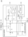
- FIG. 2 depicts an electronic system 200 in accordance with another exemplary embodiment of the present invention.
- the power regulator 202 has a first power MOS transistor (e.g., a PMOS transistor) M1, and a second power MOS transistor (e.g., another PMOS) M2.
- the first power MOS transistor M1 has a source terminal coupled to the power voltage Vin, and a drain terminal coupled to the first capacitor C 1 through the first output terminal Vo1 of the power regulator 202.
- the second power MOS transistor M2 has a source terminal coupled to the power voltage Vin, a gate terminal coupled to the gate terminal of the first power MOS transistor M1, and a drain terminal coupled to the second capacitor C2 through the second output terminal Vo2 of the power regulator 202.
- the second power MOS transistor M2 is turned off while the power regulator 202 operates in the second power mode, to disconnect the second capacitor C2 from the power regulator 202.
- the power regulator 202 further has a first switch S1, and a second switch S2.
- the first switch S1 is coupled between the gate terminal of the first power MOS transistor M1 and the gate terminal of the second power MOS transistor M2.
- the first switch S1 is closed while the power regulator 202 operates in the first power mode, and is open while the power regulator 202 operates in the second power mode.
- the second switch S2 is closed while the power regulator 202 operates in the second power mode to couple the gate terminal of the second power MOS transistor M2 to the power voltage Vin.
- the second power MOS transistor M2 is indeed turned off, and the second capacitor C2 is completely disconnected from the power regulator 202.
- the load 206 has a first power terminal Vi1 coupled to the first output terminal Vo1 of the power regulator 202, and a second power terminal Vi2 coupled to the second output terminal Vo2 of the power regulator 202.
- the load 206 has circuitry 212, receiving power from the first power terminal Vi1 and the second power terminal Vi2.
- a third switch S3 is coupled between the second power terminal Vi2 and the circuitry 212. While the power regulator 202 operates in the first power mode, the third switch S3 is closed. While the power regulator 202 operates in the second power mode, the third switch S3 is open. The third switch S3 is optional.
- FIG. 2 shows a charge supplier 210 incorporated into the power regulator 202.
- the charge supplier 210 is powered by the power voltage Vin provided by the battery 204. While the power regulator 202 operates in the second power mode, the charge supplier 210 is coupled to the second capacitor C2 through the second output terminal Vo2 of the power regulator 202 to compensate for leakage from the second capacitor C2.
- the charge supplier 210 has a current source Ibias, a fourth switch S4, and a comparator Comp.
- the current source Ibias is driven by the power voltage Vin. While the power regulator 202 operates in the second power mode, the fourth switch S4 is turned on to couple the current source Ibias to the second capacitor C2 through the second output terminal Vo2 of the power regulator 202, to compensate for leakage from the second capacitor C2.
- the comparator Comp is provided to generate a control signal CS to control the current source Ibias.
- the comparator Comp has a first input terminal ⁇ -' coupled to the second output terminal Vo2 of the power regulator 202 through the fourth switch S4, and a second input terminal ⁇ +' biased at a reference voltage Vref.
- the current source Ibias can adaptively compensate for the leakage loss.
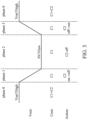
- FIG. 3 illustrates the control scheme of the output capacitance device 108 in accordance with an exemplary embodiment of the present invention.
- phase 0 the power regulator 102 is in the first power mode.
- phase 2 the power regulator 102 is in the second power mode.
- Phase 1 is a voltage-falling phase for switching from the first power mode to the second power mode.
- the second capacitor C2 is changed (from on to off) to be disconnected from the power regulator 102.
- Phase 3 is a voltage- rising phase for switching from the second power mode to the first power mode.
- the second capacitor C2 is changed (from off to on) to be coupled to the power regulator 102.
Landscapes
- Engineering & Computer Science (AREA)
- Physics & Mathematics (AREA)
- Electromagnetism (AREA)
- General Physics & Mathematics (AREA)
- Radar, Positioning & Navigation (AREA)
- Automation & Control Theory (AREA)
- Continuous-Control Power Sources That Use Transistors (AREA)
Abstract
Description
- The present invention relates to power regulation techniques.
- A power regulator is a DC-to-DC power converter or Low Dropout regulator LDO which converts a power voltage (e.g., received from a battery) to an output voltage to drive a load.
- An inrush current may take place when switching a power regulator from a power-off mode to a power-on mode. When a dynamic voltage scaling (DVS) function is enabled, inrush current may also occur when switching the power regulator from the low-power mode to the normal-power mode.
- How to reduce the inrush current is an important topic in this technical field.
- An electronic system using a power regulator with reduced inrush current is shown.
- An electronic system in accordance with an exemplary embodiment of the present invention has a power regulator, and an output capacitance device that is coupled between the power regulator and a load. The output capacitance device has a first capacitor and a second capacitor. When the power regulator is in the first power mode, the first capacitor and the second capacitor are both coupled to the power regulator. When the power regulator is in the second power mode, which uses less power than the first power mode, the first capacitor is still coupled to the power regulator, but the second capacitor is disconnected from the power regulator and is protected from being discharged by the power regulator.
- Thus, while the power regulator operates in the second power mode, a considerable charge is stored within the second capacitor. When the power regulator is switched back to the first power mode to raise up its output voltage, the inrush current is reduced due to the charge held by the second capacitor.
- In an exemplary embodiment, the first power mode is a power-on mode, and the second power mode is a power-off mode.
- In another exemplary embodiment, the first power mode is the normal-power mode of a dynamic voltage scaling (DVS) function, and the second power mode is the low-power mode of the DVS function.
- In an exemplary embodiment, the electronic system further has a charge supplier, which is coupled to the second capacitor while the power regulator operates in the second power mode, to compensate for leakage from the second capacitor.
- In an exemplary embodiment, the power regulator has a first power MOS transistor and a second power MOS transistor. The first power MOS transistor has a source terminal coupled to a power voltage, and a drain terminal coupled to the first capacitor through the first output terminal of the power regulator. The second power MOS transistor has a source terminal coupled to the power voltage, a gate terminal coupled to the gate terminal of the first power MOS transistor, and a drain terminal coupled to the second capacitor through the second output terminal of the power regulator. The second power MOS transistor is turned off while the power regulator operates in the second power mode.
- In an exemplary embodiment, the power regulator further has a charge supplier that is powered by the power voltage. While the power regulator operates in the second power mode, the charge supplier is coupled to the second capacitor through the second output terminal of the power regulator to compensate for leakage from the second capacitor.
- In an exemplary embodiment, the charge supplier has a current source, driven by the power voltage to compensate for leakage from the second capacitor.
- In an exemplary embodiment, the charge supplier further has a switch, and a comparator. While the power regulator operates in the second power mode, the switch is turned on to couple the current source to the second capacitor through the second output terminal of the power regulator. The comparator generates a control signal to control the current source. The comparator has a first input terminal coupled to the second output terminal of the power regulator through the switch, and a second input terminal biased at a reference voltage.
- In one embodiment, during a voltage-falling phase for switching from the first power mode to the second power mode, the second capacitor is changed to be disconnected from the power regulator. During a voltage-ri sing phase for switching from the second power mode to the first power mode, the second capacitor may be changed to be coupled to the power regulator.
- A detailed description is given in the following embodiments with reference to the accompanying drawings.
- The present invention can be more fully understood by reading the subsequent detailed description and examples with references made to the accompanying drawings, wherein:
-
FIG. 1 is a block diagram depicting anelectronic system 100 in accordance with an exemplary embodiment of the present invention; -
FIG. 2 depicts anelectronic system 200 in accordance with another exemplary embodiment of the present invention; and -
FIG. 3 illustrates the control scheme of theoutput capacitance device 108 in accordance with an exemplary embodiment of the present invention. - The following description is made for the purpose of illustrating the general principles of the invention and should not be taken in a limiting sense. The scope of the invention is best determined by reference to the appended claims.
-
FIG. 1 is a block diagram depicting anelectronic system 100 in accordance with an exemplary embodiment of the present invention, which may be a cell phone, a tablet, or any mobile electronic device. Theelectronic system 100 uses apower regulator 102 to convert a power voltage Vin to an output voltage Vout to drive aload 106. The power voltage Vin may be provided by abattery 104 of theelectronic system 100. Theload 106 may be a central processing unit (CPU) or any chip in theelectronic system 100. - The
electronic system 100 further has anoutput capacitance device 108 that is coupled between thepower regulator 102 and theload 106. Instead of being implemented by one single capacitor, theoutput capacitance device 108 has a first capacitor C1 and a second capacitor C2. Thepower regulator 102 can be switched between different power modes. In the different power modes, the capacitors C1 and C2 are coupled to thepower regulator 102 in the different ways. - In an exemplary embodiment, the
power regulator 102 can be switched between the first power mode and the second power mode. The output voltage Vout in the first power mode is greater than that in the second power mode. The second power mode is more power saving than the first power mode. While thepower regulator 102 operates in the first power mode, the first capacitor C1 and the second capacitor C2 are both coupled to thepower regulator 102, and both are coupled to theload 106. While thepower regulator 102 operates in the second power mode, the first capacitor C1 is still coupled to thepower regulator 102 and theload 106, but the second capacitor C2 is disconnected from thepower regulator 102 and theload 106. In the second power mode, the second capacitor C2 is protected from being discharged by thepower regulator 102. - In this manner, while the
power regulator 102 operates in the second power mode, which uses less power than the first power mode, a considerable amount of charge is held in the isolated second capacitor C2. When thepower regulator 102 is switched back to the first power mode to raise the output voltage Vout, the second capacitor C2 is reconnected to thepower regulator 102. Because of the charges previously stored in the second capacitor C2, thepower regulator 102 switched back to the first power mode will not generate a huge inrush current. - In an exemplary embodiment, the first power mode is a power-on mode, and the second power mode is a power-off mode. In the power-off mode, the output voltage Vout is 0V. In the power-on mode, the output voltage Vout is Von volt. In a conventional technique, when switching a power regulator from the power-off mode to the power-on mode, the inrush charge, ΔQold, is Von*Ctotal, where Ctotal is C1+C2. However, in the
electronic system 100, when switching thepower regulator 102 from the power-off mode to the power-on mode, the inrush charge, ΔQnew, is Von*C1, much lower thanΔQold. The inrush current is significantly reduced. Less inrush charge is wasted. - In another exemplary embodiment, the
power regulator 102 operates its dynamic voltage scaling (DVS) function. The first power mode is the normal-power mode, and the second power mode is the low-power mode. In the normal-power mode, the output voltage Vout is Vhigh volt. In the low-power mode, the output voltage Vout is Vlow volt. In a conventional technique, when switching a power regulator from the low-power mode to the normal-power mode, the inrush charge, ΔQold, is (Vhigh-Vlow)*Ctotal, where Ctotal is C1+C2. However, in theelectronic system 100, when switching thepower regulator 102 from the low-power mode to the normal-power mode, the inrush charge, ΔQnew, is (Vhigh-Vlow)*C1, much lower thanΔQold. The inrush current is significantly reduced. Less inrush charge is wasted. - As shown, the
electronic system 100 further has acharge supplier 110. Thecharge supplier 110 is coupled to the second capacitor C2 while thepower regulator 102 operates in the second power mode, to compensate for leakage from the isolated second capacitor C2. Thebattery 104 can also provide power to thecharge supplier 104. - In some other examples, the second capacitor C2 is still coupled to the
load 106 while thepower regulator 102 operates in the second power mode. -
FIG. 2 depicts anelectronic system 200 in accordance with another exemplary embodiment of the present invention. - The
power regulator 202 has a first power MOS transistor (e.g., a PMOS transistor) M1, and a second power MOS transistor (e.g., another PMOS) M2. The first power MOS transistor M1 has a source terminal coupled to the power voltage Vin, and a drain terminal coupled to thefirst capacitor C 1 through the first output terminal Vo1 of thepower regulator 202. The second power MOS transistor M2 has a source terminal coupled to the power voltage Vin, a gate terminal coupled to the gate terminal of the first power MOS transistor M1, and a drain terminal coupled to the second capacitor C2 through the second output terminal Vo2 of thepower regulator 202. The second power MOS transistor M2 is turned off while thepower regulator 202 operates in the second power mode, to disconnect the second capacitor C2 from thepower regulator 202. - In this example, the
power regulator 202 further has a first switch S1, and a second switch S2. The first switch S1 is coupled between the gate terminal of the first power MOS transistor M1 and the gate terminal of the second power MOS transistor M2. The first switch S1 is closed while thepower regulator 202 operates in the first power mode, and is open while thepower regulator 202 operates in the second power mode. The second switch S2 is closed while thepower regulator 202 operates in the second power mode to couple the gate terminal of the second power MOS transistor M2 to the power voltage Vin. Thus, in the second power mode, the second power MOS transistor M2 is indeed turned off, and the second capacitor C2 is completely disconnected from thepower regulator 202. - In
FIG. 2 , theload 206 has a first power terminal Vi1 coupled to the first output terminal Vo1 of thepower regulator 202, and a second power terminal Vi2 coupled to the second output terminal Vo2 of thepower regulator 202. Theload 206 hascircuitry 212, receiving power from the first power terminal Vi1 and the second power terminal Vi2. A third switch S3 is coupled between the second power terminal Vi2 and thecircuitry 212. While thepower regulator 202 operates in the first power mode, the third switch S3 is closed. While thepower regulator 202 operates in the second power mode, the third switch S3 is open. The third switch S3 is optional. -
FIG. 2 shows acharge supplier 210 incorporated into thepower regulator 202. Thecharge supplier 210 is powered by the power voltage Vin provided by thebattery 204. While thepower regulator 202 operates in the second power mode, thecharge supplier 210 is coupled to the second capacitor C2 through the second output terminal Vo2 of thepower regulator 202 to compensate for leakage from the second capacitor C2. - The details of the
charge supplier 210 are described in this paragraph. Thecharge supplier 210 has a current source Ibias, a fourth switch S4, and a comparator Comp. The current source Ibias is driven by the power voltage Vin. While thepower regulator 202 operates in the second power mode, the fourth switch S4 is turned on to couple the current source Ibias to the second capacitor C2 through the second output terminal Vo2 of thepower regulator 202, to compensate for leakage from the second capacitor C2. The comparator Comp is provided to generate a control signal CS to control the current source Ibias. The comparator Comp has a first input terminal `-' coupled to the second output terminal Vo2 of thepower regulator 202 through the fourth switch S4, and a second input terminal `+' biased at a reference voltage Vref. In this structure, when the second capacitor C2 isolated from thepower regulator 202 in the second power mode drops to the lower voltage level, the current source Ibias can adaptively compensate for the leakage loss. -
FIG. 3 illustrates the control scheme of theoutput capacitance device 108 in accordance with an exemplary embodiment of the present invention. - In
phase 0, thepower regulator 102 is in the first power mode. Inphase 2, thepower regulator 102 is in the second power mode.Phase 1 is a voltage-falling phase for switching from the first power mode to the second power mode. Duringphase 1, the second capacitor C2 is changed (from on to off) to be disconnected from thepower regulator 102.Phase 3 is a voltage- rising phase for switching from the second power mode to the first power mode. Duringphase 3, the second capacitor C2 is changed (from off to on) to be coupled to thepower regulator 102. - While the invention has been described by way of example and in terms of the preferred embodiments, it should be understood that the invention is not limited to the disclosed embodiments. On the contrary, it is intended to cover various modifications and similar arrangements (as would be apparent to those skilled in the art). Therefore, the scope of the appended claims should be accorded the broadest interpretation so as to encompass all such modifications and similar arrangements.
Claims (15)
- An electronic system, comprising:a power regulator; andan output capacitance device, coupled between the power regulator and a load;wherein:the output capacitance device comprises a first capacitor and a second capacitor;when the power regulator is in a first power mode, the first capacitor and the second capacitor are both coupled to the power regulator; andwhen the power regulator is in a second power mode, which uses less power than the first power mode, the first capacitor is coupled to the power regulator, and the second capacitor is disconnected from the power regulator and is protected from being discharged by the power regulator.
- The electronic system as claimed in claim 1, wherein:the first power mode is a power-on mode; andthe second power mode is a power-off mode.
- The electronic system as claimed in claim 1, wherein:the first power mode is a normal-power mode of a dynamic voltage scaling function; andthe second power mode is a low-power mode of the dynamic voltage scaling function.
- The electronic system as claimed in any one of the preceding claims, further comprising:
a charge supplier, coupled to the second capacitor while the power regulator operates in the second power mode, to compensate for leakage from the second capacitor. - The electronic system as claimed in claim 4, further comprising:
a battery, providing power to the charge supplier to compensate for leakage of the second capacitor. - The electronic system as claimed in any one of the preceding claims, wherein:while the power regulator operates in the first power mode, the first capacitor and the second capacitor are both further coupled to the load; andwhile the power regulator operates in the second power mode, the first capacitor is still coupled to the load, but the second capacitor is disconnected from the load.
- The electronic system as claimed in any one of claims 1 to 5, wherein:while the power regulator operates in the first power mode, the first capacitor and the second capacitor are both further coupled to the load; andwhile the power regulator operates in the second power mode, the first capacitor and the second capacitor are both kept coupled to the load.
- The electronic system as claimed in any one of the preceding claims, wherein the power regulator comprises:a first power MOS transistor, having a source terminal coupled to a power voltage, and a drain terminal coupled to the first capacitor through a first output terminal of the power regulator;a second power MOS transistor, having a source terminal coupled to the power voltage, a gate terminal coupled to a gate terminal of the first power MOS transistor, and a drain terminal coupled to the second capacitor through a second output terminal of the power regulator;wherein the second power MOS transistor is turned off while the power regulator operates in the second power mode.
- The electronic system as claimed in claim 8, wherein the power regulator further comprises:a first switch, coupled between the gate terminal of the first power MOS transistor and the gate terminal of the second power MOS transistor, wherein the first switch is closed while the power regulator operates in the first power mode, and is open while the power regulator operates in the second power mode; anda second switch, which is closed while the power regulator operates in the second power mode to couple the gate terminal of the second power MOS transistor to the power voltage.
- The electronic system as claimed in claim 8 or 9, wherein:
the load has a first power terminal coupled to the first output terminal of the power regulator, and a second power terminal coupled to the second output terminal of the power regulator. - The electronic system as claimed in claim 10, wherein the load further comprises:circuitry, receiving power from the first power terminal and the second power terminal; anda third switch, coupled between the second power terminal and the circuitry, wherein:while the power regulator operates in the first power mode, the third switch is closed; andwhile the power regulator operates in the second power mode, the third switch is open.
- The electronic system as claimed in any one of claims 8 to 11, wherein the power regulator further comprises:a charge supplier, powered by the power voltage,wherein while the power regulator operates in the second power mode, the charge supplier is coupled to the second capacitor through the second output terminal of the power regulator to compensate for leakage from the second capacitor.
- The electronic system as claimed in claim 12, further comprising:
a battery, providing the power voltage. - The electronic system as claimed in claim 12 or 13, wherein the charge supplier comprises:
a current source, driven by the power voltage to compensate for leakage from the second capacitor. - The electronic system as claimed in claim 14, wherein the charge supplier further comprises:a fourth switch, turned on while the power regulator operates in the second power mode, to couple the current source to the second capacitor through the second output terminal of the power regulator; anda comparator, generating a control signal to control the current source;wherein the comparator has a first input terminal coupled to the second output terminal of the power regulator through the fourth switch, and a second input terminal biased at a reference voltage.
Applications Claiming Priority (2)
| Application Number | Priority Date | Filing Date | Title |
|---|---|---|---|
| US202263367656P | 2022-07-05 | 2022-07-05 | |
| US18/320,442 US20240012438A1 (en) | 2022-07-05 | 2023-05-19 | Electronic system using a power regulator with reduced inrush current |
Publications (1)
| Publication Number | Publication Date |
|---|---|
| EP4303689A1 true EP4303689A1 (en) | 2024-01-10 |
Family
ID=86693069
Family Applications (1)
| Application Number | Title | Priority Date | Filing Date |
|---|---|---|---|
| EP23177357.3A Pending EP4303689A1 (en) | 2022-07-05 | 2023-06-05 | An electronic system using a power regulator with reduced inrush current |
Country Status (2)
| Country | Link |
|---|---|
| US (1) | US20240012438A1 (en) |
| EP (1) | EP4303689A1 (en) |
Citations (3)
| Publication number | Priority date | Publication date | Assignee | Title |
|---|---|---|---|---|
| US20100026252A1 (en) * | 2008-08-04 | 2010-02-04 | Ying-Yao Lin | Low Drop-Out Voltage Regulator with Efficient Frequency Compensation |
| US20170052552A1 (en) * | 2015-08-21 | 2017-02-23 | Qualcomm Incorporated | Single ldo for multiple voltage domains |
| US9645591B2 (en) * | 2014-01-09 | 2017-05-09 | Qualcomm Incorporated | Charge sharing linear voltage regulator |
Family Cites Families (4)
| Publication number | Priority date | Publication date | Assignee | Title |
|---|---|---|---|---|
| US8901904B2 (en) * | 2009-04-15 | 2014-12-02 | Linear Technology Corporation | Voltage and current regulators with switched output capacitors for multiple regulation states |
| US9069365B2 (en) * | 2012-02-18 | 2015-06-30 | R2 Semiconductor, Inc. | DC-DC converter enabling rapid output voltage changes |
| EP2759900B1 (en) * | 2013-01-25 | 2017-11-22 | Dialog Semiconductor GmbH | Maintaining the resistor divider ratio during start-up |
| KR20200010830A (en) * | 2018-07-23 | 2020-01-31 | 삼성전자주식회사 | Switching regulator for dynamically changing output voltage and power supply circuit including the same |
-
2023
- 2023-05-19 US US18/320,442 patent/US20240012438A1/en active Pending
- 2023-06-05 EP EP23177357.3A patent/EP4303689A1/en active Pending
Patent Citations (3)
| Publication number | Priority date | Publication date | Assignee | Title |
|---|---|---|---|---|
| US20100026252A1 (en) * | 2008-08-04 | 2010-02-04 | Ying-Yao Lin | Low Drop-Out Voltage Regulator with Efficient Frequency Compensation |
| US9645591B2 (en) * | 2014-01-09 | 2017-05-09 | Qualcomm Incorporated | Charge sharing linear voltage regulator |
| US20170052552A1 (en) * | 2015-08-21 | 2017-02-23 | Qualcomm Incorporated | Single ldo for multiple voltage domains |
Also Published As
| Publication number | Publication date |
|---|---|
| US20240012438A1 (en) | 2024-01-11 |
Similar Documents
| Publication | Publication Date | Title |
|---|---|---|
| US11606032B2 (en) | Adaptive combination power supply circuit and charging architecture | |
| US7550954B2 (en) | Method and circuit for a voltage supply for real time clock circuitry based on voltage regulated charge pump | |
| US8508963B2 (en) | Step-down switching regulator capable of providing high-speed response with compact structure | |
| US7646179B2 (en) | Electric power supply circuit and electronic device | |
| US20210067033A1 (en) | Differential sensing and maintenance of flying capacitor voltage in a switched-mode power supply circuit | |
| US7940118B1 (en) | Dying gasp charge controller | |
| US6504422B1 (en) | Charge pump with current limiting circuit | |
| US7928715B2 (en) | Switching regulator | |
| US7741818B2 (en) | Voltage regulator including an output unit for converting input voltage into a predetermined voltage and for outputting the converted voltage | |
| CN112640281B (en) | Digitally Assisted Dynamic Multi-Mode Power Supply Circuit | |
| KR20050039577A (en) | Power supply apparatus capable of supplying a stable converted voltage | |
| KR100897636B1 (en) | Charge pump device, display driver, display module and communication terminal having the device | |
| US8026703B1 (en) | Voltage regulator and method having reduced wakeup-time and increased power efficiency | |
| TW202414980A (en) | High-side n-type power transistor gate driving techniques without a bootstrap capacitor | |
| CN111600481B (en) | Voltage boosting and reducing control system of power supply and control method thereof | |
| US20110127978A1 (en) | Pwm controller with low uvlo voltage | |
| US20250167659A1 (en) | Power supply circuit, control method therefor, and electronic device | |
| US20240012438A1 (en) | Electronic system using a power regulator with reduced inrush current | |
| US8294436B2 (en) | DC/DC converter and method for controlling a DC/DC converter | |
| US20250385609A1 (en) | DC-DC Converter, Chip, and Electronic Device | |
| EP1691472B1 (en) | Self regulating charge pump | |
| CN115149787B (en) | Voltage regulating circuit and electronic equipment | |
| US20060267670A1 (en) | Semiconductor circuit apparatus | |
| US12095364B2 (en) | Voltage regulator with reduced power loss and chip using the voltage regulator | |
| US12597784B2 (en) | Power supply circuit with short circuit protection |
Legal Events
| Date | Code | Title | Description |
|---|---|---|---|
| PUAI | Public reference made under article 153(3) epc to a published international application that has entered the european phase |
Free format text: ORIGINAL CODE: 0009012 |
|
| STAA | Information on the status of an ep patent application or granted ep patent |
Free format text: STATUS: THE APPLICATION HAS BEEN PUBLISHED |
|
| AK | Designated contracting states |
Kind code of ref document: A1 Designated state(s): AL AT BE BG CH CY CZ DE DK EE ES FI FR GB GR HR HU IE IS IT LI LT LU LV MC ME MK MT NL NO PL PT RO RS SE SI SK SM TR |
|
| STAA | Information on the status of an ep patent application or granted ep patent |
Free format text: STATUS: REQUEST FOR EXAMINATION WAS MADE |
|
| 17P | Request for examination filed |
Effective date: 20240710 |
|
| RBV | Designated contracting states (corrected) |
Designated state(s): AL AT BE BG CH CY CZ DE DK EE ES FI FR GB GR HR HU IE IS IT LI LT LU LV MC ME MK MT NL NO PL PT RO RS SE SI SK SM TR |