EP4301119A1 - Josephson junction preparation method and production line device - Google Patents
Josephson junction preparation method and production line device Download PDFInfo
- Publication number
- EP4301119A1 EP4301119A1 EP23772736.7A EP23772736A EP4301119A1 EP 4301119 A1 EP4301119 A1 EP 4301119A1 EP 23772736 A EP23772736 A EP 23772736A EP 4301119 A1 EP4301119 A1 EP 4301119A1
- Authority
- EP
- European Patent Office
- Prior art keywords
- strip
- shaped
- substrate
- photoresist
- superconducting layer
- Prior art date
- Legal status (The legal status is an assumption and is not a legal conclusion. Google has not performed a legal analysis and makes no representation as to the accuracy of the status listed.)
- Pending
Links
Images




Classifications
-
- H—ELECTRICITY
- H10—SEMICONDUCTOR DEVICES; ELECTRIC SOLID-STATE DEVICES NOT OTHERWISE PROVIDED FOR
- H10N—ELECTRIC SOLID-STATE DEVICES NOT OTHERWISE PROVIDED FOR
- H10N60/00—Superconducting devices
- H10N60/01—Manufacture or treatment
- H10N60/0912—Manufacture or treatment of Josephson-effect devices
-
- C—CHEMISTRY; METALLURGY
- C23—COATING METALLIC MATERIAL; COATING MATERIAL WITH METALLIC MATERIAL; CHEMICAL SURFACE TREATMENT; DIFFUSION TREATMENT OF METALLIC MATERIAL; COATING BY VACUUM EVAPORATION, BY SPUTTERING, BY ION IMPLANTATION OR BY CHEMICAL VAPOUR DEPOSITION, IN GENERAL; INHIBITING CORROSION OF METALLIC MATERIAL OR INCRUSTATION IN GENERAL
- C23C—COATING METALLIC MATERIAL; COATING MATERIAL WITH METALLIC MATERIAL; SURFACE TREATMENT OF METALLIC MATERIAL BY DIFFUSION INTO THE SURFACE, BY CHEMICAL CONVERSION OR SUBSTITUTION; COATING BY VACUUM EVAPORATION, BY SPUTTERING, BY ION IMPLANTATION OR BY CHEMICAL VAPOUR DEPOSITION, IN GENERAL
- C23C14/00—Coating by vacuum evaporation, by sputtering or by ion implantation of the coating forming material
- C23C14/22—Coating by vacuum evaporation, by sputtering or by ion implantation of the coating forming material characterised by the process of coating
- C23C14/225—Oblique incidence of vaporised material on substrate
-
- C—CHEMISTRY; METALLURGY
- C23—COATING METALLIC MATERIAL; COATING MATERIAL WITH METALLIC MATERIAL; CHEMICAL SURFACE TREATMENT; DIFFUSION TREATMENT OF METALLIC MATERIAL; COATING BY VACUUM EVAPORATION, BY SPUTTERING, BY ION IMPLANTATION OR BY CHEMICAL VAPOUR DEPOSITION, IN GENERAL; INHIBITING CORROSION OF METALLIC MATERIAL OR INCRUSTATION IN GENERAL
- C23C—COATING METALLIC MATERIAL; COATING MATERIAL WITH METALLIC MATERIAL; SURFACE TREATMENT OF METALLIC MATERIAL BY DIFFUSION INTO THE SURFACE, BY CHEMICAL CONVERSION OR SUBSTITUTION; COATING BY VACUUM EVAPORATION, BY SPUTTERING, BY ION IMPLANTATION OR BY CHEMICAL VAPOUR DEPOSITION, IN GENERAL
- C23C14/00—Coating by vacuum evaporation, by sputtering or by ion implantation of the coating forming material
- C23C14/22—Coating by vacuum evaporation, by sputtering or by ion implantation of the coating forming material characterised by the process of coating
- C23C14/24—Vacuum evaporation
-
- C—CHEMISTRY; METALLURGY
- C23—COATING METALLIC MATERIAL; COATING MATERIAL WITH METALLIC MATERIAL; CHEMICAL SURFACE TREATMENT; DIFFUSION TREATMENT OF METALLIC MATERIAL; COATING BY VACUUM EVAPORATION, BY SPUTTERING, BY ION IMPLANTATION OR BY CHEMICAL VAPOUR DEPOSITION, IN GENERAL; INHIBITING CORROSION OF METALLIC MATERIAL OR INCRUSTATION IN GENERAL
- C23C—COATING METALLIC MATERIAL; COATING MATERIAL WITH METALLIC MATERIAL; SURFACE TREATMENT OF METALLIC MATERIAL BY DIFFUSION INTO THE SURFACE, BY CHEMICAL CONVERSION OR SUBSTITUTION; COATING BY VACUUM EVAPORATION, BY SPUTTERING, BY ION IMPLANTATION OR BY CHEMICAL VAPOUR DEPOSITION, IN GENERAL
- C23C14/00—Coating by vacuum evaporation, by sputtering or by ion implantation of the coating forming material
- C23C14/58—After-treatment
- C23C14/5846—Reactive treatment
- C23C14/5853—Oxidation
-
- G—PHYSICS
- G03—PHOTOGRAPHY; CINEMATOGRAPHY; ANALOGOUS TECHNIQUES USING WAVES OTHER THAN OPTICAL WAVES; ELECTROGRAPHY; HOLOGRAPHY
- G03F—PHOTOMECHANICAL PRODUCTION OF TEXTURED OR PATTERNED SURFACES, e.g. FOR PRINTING, FOR PROCESSING OF SEMICONDUCTOR DEVICES; MATERIALS THEREFOR; ORIGINALS THEREFOR; APPARATUS SPECIALLY ADAPTED THEREFOR
- G03F7/00—Photomechanical, e.g. photolithographic, production of textured or patterned surfaces, e.g. printing surfaces; Materials therefor, e.g. comprising photoresists; Apparatus specially adapted therefor
- G03F7/70—Microphotolithographic exposure; Apparatus therefor
- G03F7/70008—Production of exposure light, i.e. light sources
-
- G—PHYSICS
- G03—PHOTOGRAPHY; CINEMATOGRAPHY; ANALOGOUS TECHNIQUES USING WAVES OTHER THAN OPTICAL WAVES; ELECTROGRAPHY; HOLOGRAPHY
- G03F—PHOTOMECHANICAL PRODUCTION OF TEXTURED OR PATTERNED SURFACES, e.g. FOR PRINTING, FOR PROCESSING OF SEMICONDUCTOR DEVICES; MATERIALS THEREFOR; ORIGINALS THEREFOR; APPARATUS SPECIALLY ADAPTED THEREFOR
- G03F7/00—Photomechanical, e.g. photolithographic, production of textured or patterned surfaces, e.g. printing surfaces; Materials therefor, e.g. comprising photoresists; Apparatus specially adapted therefor
- G03F7/70—Microphotolithographic exposure; Apparatus therefor
- G03F7/708—Construction of apparatus, e.g. environment aspects, hygiene aspects or materials
- G03F7/70908—Hygiene, e.g. preventing apparatus pollution, mitigating effect of pollution or removing pollutants from apparatus
- G03F7/70925—Cleaning, i.e. actively freeing apparatus from pollutants, e.g. using plasma cleaning
-
- H—ELECTRICITY
- H10—SEMICONDUCTOR DEVICES; ELECTRIC SOLID-STATE DEVICES NOT OTHERWISE PROVIDED FOR
- H10N—ELECTRIC SOLID-STATE DEVICES NOT OTHERWISE PROVIDED FOR
- H10N60/00—Superconducting devices
- H10N60/10—Junction-based devices
- H10N60/12—Josephson-effect devices
-
- Y—GENERAL TAGGING OF NEW TECHNOLOGICAL DEVELOPMENTS; GENERAL TAGGING OF CROSS-SECTIONAL TECHNOLOGIES SPANNING OVER SEVERAL SECTIONS OF THE IPC; TECHNICAL SUBJECTS COVERED BY FORMER USPC CROSS-REFERENCE ART COLLECTIONS [XRACs] AND DIGESTS
- Y10—TECHNICAL SUBJECTS COVERED BY FORMER USPC
- Y10S—TECHNICAL SUBJECTS COVERED BY FORMER USPC CROSS-REFERENCE ART COLLECTIONS [XRACs] AND DIGESTS
- Y10S505/00—Superconductor technology: apparatus, material, process
- Y10S505/80—Material per se process of making same
- Y10S505/815—Process of making per se
- Y10S505/816—Sputtering, including coating, forming, or etching
- Y10S505/817—Sputtering, including coating, forming, or etching forming josephson element
-
- Y—GENERAL TAGGING OF NEW TECHNOLOGICAL DEVELOPMENTS; GENERAL TAGGING OF CROSS-SECTIONAL TECHNOLOGIES SPANNING OVER SEVERAL SECTIONS OF THE IPC; TECHNICAL SUBJECTS COVERED BY FORMER USPC CROSS-REFERENCE ART COLLECTIONS [XRACs] AND DIGESTS
- Y10—TECHNICAL SUBJECTS COVERED BY FORMER USPC
- Y10S—TECHNICAL SUBJECTS COVERED BY FORMER USPC CROSS-REFERENCE ART COLLECTIONS [XRACs] AND DIGESTS
- Y10S505/00—Superconductor technology: apparatus, material, process
- Y10S505/825—Apparatus per se, device per se, or process of making or operating same
- Y10S505/917—Mechanically manufacturing superconductor
- Y10S505/922—Making josephson junction device
Definitions
- This disclosure relates to the field of micro-nano processing technologies, and in particular, to a method for preparing a Josephson junction and a production line device.
- a Josephson junction is a currently commonly used quantum bit structure, and may be prepared by using a pre-designed photoresist structure.
- a Dolan bridge photoresist structure pattern including an undercut may be made on a double-layer electron beam photoresist on a surface of a substrate by using an electron beam exposure method, and then a Josephson junction is prepared by using a double-dip evaporation method in which a superconducting metal film is obliquely plated, then an insulating layer is oxidized, and then the superconducting metal film is vertically evaporated.
- an extra Josephson junction (also referred to as a parasitic junction) is introduced into a prepared quantum bit assembly, thereby affecting coherence of the quantum bit assembly.
- Embodiments of this disclosure provide a method for preparing a Josephson junction and a production line device, so as to improve coherence of a quantum bit assembly.
- Technical solutions are as follows:
- a method for preparing a Josephson junction is provided, where the method is performed by a production line device, and the method includes:
- a production line device includes: a spin coater, a lithography machine, and an evaporation machine;
- a photoresist film layer of an undercut structure is prepared on a substrate, where the undercut structure has two non-parallel strip-shaped openings, and two strip-shaped superconducting layers that cross each other and are separated by an oxidation layer are prepared on the substrate in the undercut structure by means of oblique evaporation at two different angles.
- only one Josephson junction is formed at an intersection of two strip-shaped superconducting layers, and another parasitic junction is not brought, thereby improving coherence of a quantum bit assembly.
- Quantum bit In quantum informatics, it is the unit of measure of quantum information.
- a quantum bit may be in both a state of 0 and a state of 1, that is, a quantum superposition state of 0 and 1.
- Josephson junction A sandwich structure formed by stacking a superconducting layer, an insulating layer, and a superconducting layer, also referred to as a superconducting tunnel junction.
- a Josephson junction is generally a structure in which two superconductors sandwich a very thin barrier layer (thickness ⁇ coherence length of a Cooper electron pair), for example, an S (Superconductor)-I (semiconductor or insulator)-S (superconductor) structure, which is referred to as an SIS structure.
- S Superconductor
- I semiconductor or insulator
- S superconductor
- SIS superconductor
- Shadow evaporation During evaporation, an evaporation material is incident on a surface of a substrate at a specific angle.
- a barrier of a specific shape is disposed in an incident path by defining a photoresist pattern, so that a film layer is selectively evaporated on some parts of the surface of the substrate, but a film layer is not plated on other parts.
- Josephson junction patch A part of a superconducting quantum chip that connects a Josephson junction to an external circuit.
- Josephson junction bandage A part of a superconducting quantum chip that connects a Josephson junction patch to an external circuit.
- Ion milling A surface of a material is bombarded with a directional ion beam to remove an oxidation layer on the surface of the material.
- Oblique evaporation A film is evaporated for an evaporation material in a direction non-parallel to a substrate normal.
- a film is evaporated for an evaporation material in a direction parallel to a substrate normal.
- Lift off A process in which a photoresist dissolves in a degumming solution, and a metal layer on the photoresist is also removed from a substrate.
- Decoherence The ability of a quantum bit to maintain association between different quantum states.
- Undercut structure A pattern structure formed after a photoresist is developed, where a size of an upper opening is smaller than a size of a lower opening.
- a multi-step process is performed in a single vacuum chamber or in a plurality of interconnected vacuum chambers in which a sample/product is not moved to an atmospheric environment.
- Quantum computers have received wide attention because they are significantly faster than classical computers in dealing with some specific problems.
- a possible way to implement a quantum computer is a superconducting quantum computer.
- Superconducting quantum computers rely on superconducting quantum chips to implement logic gate operations.
- a superconducting quantum chip may be simply considered to be composed of an external circuit and a Josephson junction, where the Josephson junction is a core element of the superconducting quantum chip.
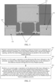
- FIG. 1 is a diagram of a preparation effect of a Josephson junction according to this disclosure.
- FIG. 1 shows two Josephson junctions 101 in parallel, which are connected to an external circuit via a Josephson junction patch 102. As shown in FIG.
- a parasitic junction 103 is formed in a quantum bit assembly, and the parasitic junction is shown in a dashed line box part in FIG. 1 .
- a large-area parasitic junction is introduced into a quantum bit assembly that includes the Josephson junction, thereby affecting decoherence of the quantum bit assembly, and further affecting performance of a quantum computing device.
- subsequent embodiments of this disclosure provide a new Josephson junction preparation solution.
- the solutions provided in subsequent embodiments of this disclosure are applicable to preparation of a superconducting quantum chip such as a plane, flip chip bonding, or a multilayer stack.
- FIG. 2 is a method flowchart of a method for preparing a Josephson junction according to an exemplary embodiment of this disclosure.
- the method may be performed by a production line device.
- the method may include the following steps: Step 201: Prepare a photoresist film layer including an undercut structure on a substrate; the undercut structure including a first strip-shaped opening and a second strip-shaped opening; and the first strip-shaped opening being non-parallel to the second strip-shaped opening.
- the undercut structure may mean that different degrees of exposure are performed on a pattern designed in two or more layers of photoresist on the substrate, so as to form a cavity under an upper-layer photoresist, and form one or more opening photoresist structures less than the cavity in the upper-layer photoresist.
- FIG. 3 is a schematic diagram of an undercut structure according to an embodiment of this disclosure.
- an undercut structure 33 is formed.
- An area of a lower half of the undercut structure 33 is greater than an area of an upper half of the undercut structure 33.
- the undercut structure in the photoresist film layer that is of the undercut structure and that is prepared on the substrate, the undercut structure includes two strip-shaped openings, where the two strip-shaped openings are non-parallel, that is, one ends of the strip-shaped openings are close to each other, and the other ends of the strip-shaped openings are far from each other.
- Step 202 Perform, at a first angle, evaporation on the photoresist film layer obliquely to the substrate, to prepare a first strip-shaped superconducting layer on the substrate through the first strip-shaped opening.
- a direction in which evaporation is performed at the first angle refers to a direction that is inclined to a normal direction of the substrate and that points to the substrate.
- the first strip-shaped opening is a strip
- the first strip-shaped opening is incident on the evaporation material of the first strip-shaped opening at the first angle, and a part that is not blocked by the photoresist on the upper layer of the undercut structure forms the first strip-shaped superconducting layer on the substrate.
- Step 203 Perform, at a second angle, evaporation on the photoresist film layer obliquely to the substrate, to prepare a second strip-shaped superconducting layer on the substrate through the second strip-shaped opening, wherein the first strip-shaped superconducting layer and the second strip-shaped superconducting layer are arranged to cross each other, the first strip-shaped superconducting layer being isolated (i.e., spatially and/or electrically isolated) from the second strip-shaped superconducting layer by an oxidation layer to form a Josephson junction.
- a direction in which evaporation is performed at the second angle refers to another direction that is inclined to the normal direction of the substrate and that points to the substrate.
- the second strip-shaped superconducting layer is formed on the substrate in a part that is of the evaporation material incident in the second strip-shaped opening at the second angle and that is not blocked by the photoresist on the upper layer of the undercut structure.
- Positions of the first strip-shaped superconducting layer and the second strip-shaped superconducting layer on the substrate are determined by an opening position of the undercut structure, a height of the upper-layer photoresist, a thickness of the upper-layer photoresist, and evaporation angles (that is, the first angle and the second angle).
- the opening position of the undercut structure By designing the opening position of the undercut structure, the height of the upper-layer photoresist, the thickness of the upper-layer photoresist, and the evaporation angles, the first strip-shaped superconducting layer and the second strip-shaped superconducting layer cross each other on the substrate, and as long as a region in which the two strip-shaped superconducting layers cross each other is isolated by using an oxidation layer, a Josephson junction can be formed.
- a photoresist film layer with an undercut structure is prepared on a substrate, where the undercut structure has two non-parallel strip-shaped openings, and two strip-shaped superconducting layers that cross each other and are separated by an oxidation layer are prepared on the substrate in the undercut structure by means of oblique evaporation at two different angles.
- only one Josephson junction is formed at an intersection of two strip-shaped superconducting layers, and another parasitic junction is not brought, thereby improving coherence of a quantum bit assembly.
- FIG. 4 is a flowchart of preparing a Josephson junction according to an exemplary embodiment of this disclosure.
- a preparation process of a Josephson junction may be as follows: S1. Prepare a photoresist film layer on a substrate, where the photoresist film layer includes an undercut structure, and the undercut structure includes two strip-shaped openings.
- a region in which the undercut structure on the substrate is located is a region 41, a lower part of the undercut structure is a cavity, and a part of the upper part other than a strip-shaped opening 42 and a strip-shaped opening 43 is a photoresist. A part outside the region 41 is filled with a photoresist.
- positions of the strip-shaped superconducting layers formed on the substrate after superconducting materials that are evaporated at different angles respectively pass through the strip-shaped opening 42 and the strip-shaped opening 43 are deviated from projection positions of the strip-shaped opening 42 and the strip-shaped opening 43 on the substrate, so that two superconducting layers obtained by means of evaporation by using the strip-shaped opening 42 and the strip-shaped opening 43 that do not intersect may intersect to form a Josephson junction.
- the first angle is an angle at which oblique incidence on the substrate is performed from the right side to the left side of the strip-shaped opening 42.
- the second angle is an angle at which oblique incidence on the substrate is performed from the bottom to the top of the strip-shaped opening.
- the evaporation material penetrates the strip-shaped opening 43, and a strip-shaped superconducting layer 45 is formed on the substrate above the strip-shaped opening 43.
- the first angle/the second angle may be shown in FIG. 3 .
- the strip-shaped superconducting layer 44 and the strip-shaped superconducting layer 45 may cross each other, and evaporated superconducting layers are oxidized between two times of oblique evaporation to obtain a Josephson junction 46 after the second time of oblique evaporation.
- a Josephson junction patch in addition to preparing a Josephson junction without a parasitic junction, may be further prepared without introducing the parasitic junction.
- FIG. 5 is a method flowchart of a method for preparing a Josephson junction according to an exemplary embodiment of this disclosure.
- the method may be performed by a production line device. As shown in FIG. 5 , the method may include the following steps:
- Step 501 Prepare a photoresist film layer including an undercut structure on a substrate; the undercut structure including a first strip-shaped opening and a second strip-shaped opening; and the first strip-shaped opening being non-parallel to the second strip-shaped opening.
- the undercut structure further includes a first connecting part opening and a second connecting part opening.
- an extension direction of the first strip-shaped opening is perpendicular to an extension direction of the second strip-shaped opening.
- the extension direction of the strip-shaped opening may be a direction in which a straight line segment between two ends of the strip-shaped opening continues to extend to one end/two ends.
- the extension direction of the first strip-shaped opening and the extension direction of the second strip-shaped opening may be set to be perpendicular, so that two strip-shaped superconducting layers that cross to form a Josephson junction and that are subsequently prepared are also perpendicular to each other.
- the extension direction of the first strip-shaped opening and the extension direction of the second strip-shaped opening may also be at an angle other than 90°, for example, 45°, 60°, or 80°.
- the undercut structure further includes a first connecting part opening and a second connecting part opening, where the first connecting part opening and the second connecting part opening are used for subsequently preparing Josephson junction patches separately connected to the two strip-shaped superconducting layers forming the Josephson junction.
- the preparing a photoresist film layer including an undercut structure on a substrate includes:
- a layer of first photoresist may be first spin-coated on the substrate, and the first photoresist is solidified by means of solidification processing, for example, baking processing. Then a layer of second photoresist is spin-coated on an upper layer of the first photoresist, and the second photoresist is solidified by means of solidification processing. In this way, a double-layer photoresist can be prepared on the substrate.
- the first photoresist and the second photoresist are photoresists of different materials.
- the first photoresist is located at a lower layer of the second photoresist, and an undercut structure needs to be prepared. Therefore, subsequently, the first photoresist needs to be exposed when the second photoresist is retained. Therefore, in this embodiment of this disclosure, the first photoresist may more easily reach an exposure condition than the second photoresist.
- S501e Perform electron beam exposure on the second photoresist in regions of the first strip-shaped opening and the second strip-shaped opening.
- S501f Perform electron beam exposure on the first photoresist and the second photoresist in regions of the first connecting part opening and the second connecting part opening.
- S501g Perform, in a region of the undercut structure, electron beam exposure on the first photoresist in a region other than the first connecting part opening and the second connecting part opening.
- a lithography machine may separately use exposure processing of different degrees for the strip-shaped opening, the connecting part opening, and another part of the undercut structure (that is, a cavity part that is blocked above), so that the foregoing three different positions have different exposure effects.
- the lithography machine may first perform exposure on the first photoresist, and an exposure region includes another region in the undercut structure except the connecting part opening. Then, the lithography machine performs exposure on the second photoresist, and an exposure region includes a region corresponding to the strip-shaped opening. After the foregoing two times of exposure, a region of the connecting part opening is not exposed. In this case, the lithography machine may simultaneously expose the first photoresist and the second photoresist in the region of the connecting part opening.
- the plurality of exposure steps may also be simultaneously performed by the lithography machine, that is, the lithography machine may simultaneously expose the first photoresist in the region other than the connecting part opening in the undercut structure, the second photoresist in the region corresponding to the strip-shaped opening, and the first photoresist and the second photoresist in the region of the connecting part opening.
- an operator or an operation device may perform developing processing on the photoresist on the substrate, to remove the exposed photoresist, and leave the photoresist film layer including the undercut structure.
- the developing the first photoresist and the second photoresist that are obtained after electron beam exposure, to obtain the photoresist film layer including the undercut structure includes:
- the exposed first photoresist and the exposed second photoresist may be first placed in a developing solution for development for a period of time, to remove most of the exposed photoresist, and the remaining developed photoresist may be further cleaned by using oxygen plasma.
- Step 502 Perform, at a first angle, evaporation on the photoresist film layer obliquely to the substrate, to prepare a first strip-shaped superconducting layer on the substrate through the first strip-shaped opening.
- the undercut structure further includes a second strip-shaped opening. Therefore, in a process of performing, at the first angle, evaporation on the photoresist film layer obliquely to the substrate, a third strip-shaped superconducting layer is further prepared on the substrate by using the second strip-shaped opening.
- first strip-shaped opening and the second strip-shaped opening do not intersect, for oblique evaporation at the same angle, two strip-shaped superconducting layers prepared on the substrate through the two strip-shaped openings also do not intersect.
- Step 503 Perform oxidation processing on the first strip-shaped superconducting layer to prepare the oxidation layer on a surface of the first strip-shaped superconducting layer.
- a to-be-prepared Josephson junction includes two parts of superconducting materials and an insulating layer between the two parts of superconducting materials. Therefore, before the second strip-shaped superconducting layer is prepared, an oxidation layer may be first prepared on a surface of the first strip-shaped superconducting layer to serve as an insulating layer in the Josephson junction.
- Step 504 Perform, at a second angle, evaporation on the photoresist film layer obliquely to the substrate, to prepare a second strip-shaped superconducting layer on the substrate through the second strip-shaped opening; the first strip-shaped superconducting layer and the second strip-shaped superconducting layer are arranged to cross each other, the first strip-shaped superconducting layer being isolated from the second strip-shaped superconducting layer by an oxidation layer to form a Josephson junction.
- a fourth strip-shaped superconducting layer is further prepared on the substrate through the first strip-shaped opening.
- the third strip-shaped superconducting layer does not intersect the first strip-shaped superconducting layer and the second strip-shaped superconducting layer, and correspondingly, the fourth strip-shaped superconducting layer does not intersect the first strip-shaped superconducting layer and the second strip-shaped superconducting layer.
- each strip-shaped superconducting layer is formed on the substrate, including the first strip-shaped superconducting layer and the second strip-shaped superconducting layer that intersect each other, and the independent third strip-shaped superconducting layer and the independent fourth strip-shaped superconducting layer.
- the first strip-shaped superconducting layer and the second strip-shaped superconducting layer that intersect each other are used for forming a Josephson junction, and the third strip-shaped superconducting layer and the fourth strip-shaped superconducting layer are not to be connected to a to-be-prepared quantum bit assembly.
- Step 505 Perform ion milling cleaning on the first strip-shaped superconducting layer and the second strip-shaped superconducting layer.
- the production line device may perform ion milling cleaning on an overlapping region of the first strip-shaped superconducting layer and the projection of the first connecting part opening on the substrate, and an overlapping region of the second strip-shaped superconducting layer and the projection of the second connecting part opening on the substrate.
- a subsequently to-be-prepared Josephson junction patch needs to form a superconducting connection to the Josephson junction, an oxidation step exists in a process of preparing the Josephson junction, that is, an oxidation layer exists on a surface of the first strip-shaped superconducting layer. Therefore, in this embodiment of this disclosure, before the Josephson junction patch is prepared, ion milling cleaning is first performed on the prepared first strip-shaped superconducting layer and the prepared second strip-shaped superconducting layer, to remove the oxidation layer on the surface of the first strip-shaped superconducting layer.
- an oxidation layer is also prepared on surfaces of the third strip-shaped superconducting layer and the fourth strip-shaped superconducting layer.
- a direction of ion milling cleaning may be a direction perpendicular to the substrate, and correspondingly, a cleaned region includes a region that is not blocked by the photoresist in the vertical direction, that is, a region in which the first strip-shaped superconducting layer overlaps a vertical projection of the first connecting part opening on the substrate (that is, a region in which the vertical projection of the first connecting part opening on the substrate overlaps the first strip-shaped superconducting layer on the substrate), a region in which the second strip-shaped superconducting layer overlaps a vertical projection of the second connecting part opening on the substrate (that is, a region in which the vertical projection of the second connecting part opening on the substrate overlaps the second strip-shaped superconducting layer on the substrate), a region of a vertical projection of the third strip-shaped superconducting layer on the substrate, and a region of a vertical projection of the fourth strip-shaped superconducting layer on the substrate.
- Step 506 Perform evaporation perpendicular to the substrate on the photoresist film layer, so as to prepare a first connecting-part superconducting layer and a second connecting-part superconducting layer on the substrate through the first connecting part opening and the second connecting part opening; the first connecting-part superconducting layer and the first strip-shaped superconducting layer forming a superconducting connection; and the second connecting-part superconducting layer and the second strip-shaped superconducting layer forming a superconducting connection.
- the position of the vertical projection of the first connecting part opening on the substrate intersects the first strip-shaped superconducting layer, and the position of the vertical projection of the second connecting part opening on the substrate also intersects the second strip-shaped superconducting layer.
- This may be implemented by designing the first angle and the second angle.
- the evaporated superconducting material may be used for preparing, on the substrate, the first connecting-part superconducting layer that forms a superconducting connection to the first strip-shaped superconducting layer, and a second connecting-part superconducting layer that forms a superconducting connection to the second strip-shaped superconducting layer.
- an execution environment of the steps (that is, step 502 to step 506) from performing, at the first angle, evaporation on the photoresist film layer obliquely to the upper surface of the substrate (also referred to as oblique evaporation) to performing evaporation perpendicular to the substrate on the photoresist film layer (also referred to as straight evaporation) is an in situ environment.
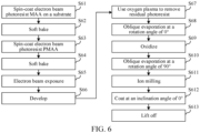
- FIG. 6 is a process flowchart of preparing a Josephson junction according to an embodiment of this disclosure.
- a Josephson junction is prepared in a manner of designing a shadow evaporation.
- FIG. 6 an example in which two strip-shaped openings are perpendicular to each other is used.
- a specific process thereof may be as follows:
- An electron beam exposure dose may be as follows: An exposure dose of the PMMA photoresist in the strip-shaped opening region is 450 ⁇ C/cm ⁇ 2. An exposure dose of the MAA photoresist in the region of the undercut structure except the connecting part opening is 150 ⁇ C/cm ⁇ 2. An exposure dose of the PMMA+MAA photoresist in the region of the connecting part opening is 800 ⁇ C/cm ⁇ 2.
- exposure may be performed on the PMMA+MAA photoresist in the regions of the strip-shaped opening and the connecting part opening, and MAA in other regions in the undercut structure.
- a sample with a graphic structure is put into a vacuum chamber that integrates ion milling, oxidation, and multi-angle coating functions for vacuuming.
- an angle 30° between an ion incident direction and a substrate normal direction may be set, and a substrate rotation rate 10 rpm may be set.
- the purpose of ion milling is to remove an oxidation layer on a surface of an external circuit.
- the first connecting part opening is not connected to the first strip-shaped opening, and the second connecting part opening is not connected to the second strip-shaped opening;
- the first strip-shaped superconducting layer and a projection of the first strip-shaped opening on the substrate do not intersect; and the second strip-shaped superconducting layer and a projection of the second strip-shaped opening on the substrate do not intersect.
- FIG. 7 shows a pattern used for electron beam exposure according to an embodiment of this disclosure.
- a region 71 indicates a region in which an electron beam photoresist at an MAA layer disappears after development
- a region 72 indicates a region in which an electron beam photoresist at a PMMA layer disappears after development
- a region 73 indicates a region in which an electron beam photoresist at a PMMA+MAA layer disappears after development.
- the remaining blank region indicates a region in which both PMMA and MAA remain after development.
- FIG. 8 is a cross-sectional view of an undercut structure according to an embodiment of this disclosure. As shown in FIG. 8 , the section is a section at a tangent 74 in FIG. 7 .
- a region 81 represents a MAA layer electron beam photoresist that remains after development
- a region 82 represents a PMMA layer electron beam photoresist that remains after development
- a region 83 represents a substrate.
- a small quantity of residual electron beam photoresist in a surface exposure region of the substrate 83 is cleaned by using oxygen plasma, and the structure is put into a device that integrates ion milling, oxidation, and multi-angle coating functions for vacuuming.
- a rotation angle may be set to 0°, and an inclination angle may be set to ⁇ for coating.
- the rotation angle being 0° may indicate a rotation angle at which an evaporation angle is perpendicular to an extension direction of a strip-shaped opening.
- the rotation angle is 90°, the evaporation angle is perpendicular to an extension direction of another strip-shaped opening.
- FIG. 9 is a schematic diagram of evaporation according to an embodiment of this disclosure.
- an evaporation source 91 with a rotatable angle is added on the basis of FIG. 8 .
- a width of an MAA graphics definition layer 81 is d_M
- a width of a PMMA graphics definition layer 82 is d_P
- a width of the Josephson junction 92 is defined as d_P-t_P ⁇ tan ⁇ , and the width of the Josephson junction may be adjusted by adjusting the angle ⁇ on the basis of meeting the foregoing relationship.
- the substrate After oxidation, the substrate is rotated by 90°, and similarly, the angle of ⁇ can be adjusted to control a length of the Josephson junction.
- the following condition needs to be met: (t_P+t_M )tan ⁇ >d_(P+M), where d_(P+M) is the width of the PMMA+MAA graphics definition layer 73.
- an oxidation layer of an external circuit that is exposed in the region 73 is removed by using ion milling, then the inclination angle is set to 0°, and the rotation angle is set to any angle.
- a superconducting material is evaporated to form a Josephson junction bandage/patch.
- FIG. 10 is a schematic diagram of three times of coating processes according to an embodiment of this disclosure.
- a vertical evaporation identifier 1001 indicates that a superconducting film layer is evaporated along a direction perpendicular to a paper surface.
- a region 1002 represents a circuit formed after the first time of coating
- a region 1003 represents a circuit formed after the second time of coating
- a region 1004 represents a formed Josephson junction
- a region 1005 represents a Josephson junction bandage/patch formed after the third time of coating.
- FIG. 11 shows an effect diagram after a photoresist is lifted off according to an embodiment of this disclosure.
- the dashed block 1101 is a prepared Josephson junction.
- the first connecting part opening is connected to one end of the first strip-shaped opening, and the second connecting part opening is connected to one end of the second strip-shaped opening;
- That the projection of the evaporation direction at the first angle on the substrate is parallel to the direction in which the first strip-shaped opening extends from the first connecting part opening to the other end of the first strip-shaped opening means that a direction obtained by projecting the evaporation direction at the first angle on the substrate is parallel to the direction in which the first strip-shaped opening extends from the first connecting part opening to the other end of the first strip-shaped opening, and also means that the projection of the evaporation direction at the first angle on the substrate is the same as the extension direction of the first strip-shaped opening from the first connecting part opening to the other end of the first strip-shaped opening.
- the position of the junction region of the Josephson junction is defined under a hollow photoresist structure by using the shadow evaporation method, so as to avoid damage to the Josephson junction caused by ion bombardment. Therefore, in addition to the implementation solutions shown in FIG. 7 to FIG. 10 , the Josephson junction may be implemented by using another similar solution, provided that the Josephson junction is prepared under the upper-layer photoresist in the undercut structure in a manner of oblique evaporation. The following provides a possible alternative solution.
- FIG. 12 is a schematic diagram of an undercut pattern and three times of coating processes according to an embodiment of this disclosure. As shown in FIG. 12 , the section shown in FIG. 8 is still used as an example. Requirements for an evaporation angle and an opening size of the section are as follows: t_P ⁇ tan ⁇ >d_P, and (t_P+t_M)tan ⁇ >d_(P+M).
- a rotation angle is set to 90°, and an inclination angle ⁇ is set to any value that meets the foregoing requirements.
- the rotation angle is set to 0°, and the inclination angle ⁇ is set to any value that meets the foregoing requirements.
- the first two times of evaporation form a Josephson junction.
- ion milling is performed to remove an oxidation layer in contact with an external circuit.
- the rotation angle is set to any angle, and the inclination angle is set to 0°, to form a Josephson junction patch/bandage.
- FIG. 13 is an effect diagram after a photoresist is lifted off according to an embodiment of this disclosure.
- a photoresist film layer with an undercut structure that has two non-parallel strip-shaped openings is prepared on a substrate, and two strip-shaped superconducting layers that cross each other and are isolated by an oxidation layer between the first strip-shaped superconducting layer and the second strip-shaped superconducting layer are prepared on the substrate in the undercut structure by means of oblique evaporation at two different angles.
- only one Josephson junction is formed at an intersection of two strip-shaped superconducting layers, and another parasitic junction is not brought, thereby improving coherence of a quantum bit assembly.
- FIG. 14 is a schematic diagram of an application scenario of a solution according to an embodiment of this disclosure.
- the application scenario may be a superconducting quantum computing platform, and the application scenario includes: a quantum computing device 141, a dilution refrigerator 142, a control device 143, and a computer 144.
- the quantum computing device 141 is a circuit that acts on a physical quantum bit.
- the quantum computing device 141 may be implemented as a quantum chip, for example, a superconducting quantum chip that is near absolute zero.
- the dilution refrigerator 142 is configured to provide an absolute zero environment for a superconducting quantum chip.
- the physical quantum bit may be a Josephson junction prepared by using the method shown in the foregoing embodiment of this disclosure.
- the control device 143 is configured to control the quantum computing device 141, and the computer 144 is configured to control the control device 143.
- a compiled quantum program is interpreted by software in the computer 144 into an instruction and sent to the control device 143 (for example, an electronic/microwave control system), and the control device 143 converts the instruction into an electronic/microwave control signal and inputs the electronic/microwave control signal to the dilution refrigerator 142 to control a superconducting quantum bit at a temperature less than 10 mK.
- a read waveform is transferred to the quantum computing device 141 in a reading process.
- FIG. 15 is a schematic diagram of a production line device according to an exemplary embodiment of this disclosure. As shown in FIG. 15 , the production line device includes: a spin coater 1501, a lithography machine 1502, and an evaporation machine 1503;
- the evaporation machine 1503 in a process of performing, at the first angle, evaporation on the photoresist film layer obliquely to the substrate, is further configured to prepare a third strip-shaped superconducting layer on the substrate through the second strip-shaped opening; and the third strip-shaped superconducting layer does not intersect the first strip-shaped superconducting layer and the second strip-shaped superconducting layer.
- the evaporation machine 1503 in a process of performing, at the second angle, evaporation on the photoresist film layer obliquely to the substrate, is further configured to prepare a fourth strip-shaped superconducting layer on the substrate through the first strip-shaped opening; and the fourth strip-shaped superconducting layer does not intersect the first strip-shaped superconducting layer and the second strip-shaped superconducting layer.
- the evaporation machine 1503 is further configured to: before performing, at the second angle, evaporation on the photoresist film layer obliquely to the substrate, perform oxidation processing on the first strip-shaped superconducting layer to prepare the oxidation layer on a surface of the first strip-shaped superconducting layer.
- the first strip-shaped superconducting layer and a projection of the first strip-shaped opening on the substrate do not intersect; the second strip-shaped superconducting layer and a projection of the second strip-shaped opening on the substrate do not intersect;
- the undercut structure further includes a first connecting part opening and a second connecting part opening; and the evaporation machine 1503 is further configured to perform evaporation perpendicular to the substrate on the photoresist film layer, so as to prepare a first connecting-part superconducting layer and a second connecting-part superconducting layer on the substrate through the first connecting part opening and the second connecting part opening; the first connecting-part superconducting layer and the first strip-shaped superconducting layer forming a superconducting connection; and the second connecting-part superconducting layer and the second strip-shaped superconducting layer forming a superconducting connection.
- an extension direction of the first strip-shaped opening is perpendicular to an extension direction of the second strip-shaped opening.
- the first connecting part opening is not connected to the first strip-shaped opening, and the second connecting part opening is not connected to the second strip-shaped opening;
- the first connecting part opening is connected to one end of the first strip-shaped opening, and the second connecting part opening is connected to one end of the second strip-shaped opening;
- the production line device further includes: an etching machine 1504; and the etching machine 1504 is configured to: before the evaporation machine performs evaporation perpendicular to the substrate on the photoresist film layer, perform ion milling cleaning on an overlapping region of the first strip-shaped superconducting layer and the projection of the first connecting part opening on the substrate, and an overlapping region of the second strip-shaped superconducting layer and the projection of the second connecting part opening on the substrate.
- the production line device further includes a hot plate 1505;
- the photoresist film layer including the undercut structure is obtained by placing the exposed first photoresist and the exposed second photoresist into a developing solution for development, and cleaning, by using oxygen plasma, photoresist remaining on the substrate after lithographic development.
- the production line device further includes a processor, and the processor may be separately electrically connected to the spin coater 1501, the lithography machine 1502, the evaporation machine 1503, the etching machine 1504, and the hot plate 1505, so as to control the spin coater 1501, the lithography machine 1502, the evaporation machine 1503, the etching machine 1504, the hot plate 1505, and the like.
- the production line device further includes a power supply, to supply electric power to electrical devices such as the processor, the spin coater 1501, the lithography machine 1502, the evaporation machine 1503, the etching machine 1504, and the hot plate 1505.
- a power supply to supply electric power to electrical devices such as the processor, the spin coater 1501, the lithography machine 1502, the evaporation machine 1503, the etching machine 1504, and the hot plate 1505.
- a spatial connection is made between the machines by using a conveyor belt, or movement of a prepared product between the machines is completed based on a mechanical arm.
- the production line device further includes a memory.
- the memory may be configured to store at least one computer instruction, and the processor executes the at least one computer instruction, so that the production line device performs the foregoing method for preparing a Josephson junction.
- a computer readable storage medium is further provided, where the computer readable storage medium stores at least one computer instruction, and the at least one computer instruction is executed by a processor in a production line device, so that the production line device performs the foregoing method for preparing a Josephson junction.
- a computer program product or a computer program is further provided.
- the computer program product or the computer program includes computer instructions, and the computer instructions are stored in a computer readable storage medium.
- a processor of a production line device reads the computer instructions from the computer readable storage medium, and the processor executes the computer instructions, so that the production line device performs the foregoing method for preparing a Josephson junction.
Landscapes
- Chemical & Material Sciences (AREA)
- Engineering & Computer Science (AREA)
- Materials Engineering (AREA)
- Organic Chemistry (AREA)
- Mechanical Engineering (AREA)
- Chemical Kinetics & Catalysis (AREA)
- Metallurgy (AREA)
- Physics & Mathematics (AREA)
- Manufacturing & Machinery (AREA)
- Epidemiology (AREA)
- General Physics & Mathematics (AREA)
- Public Health (AREA)
- Health & Medical Sciences (AREA)
- Life Sciences & Earth Sciences (AREA)
- Environmental & Geological Engineering (AREA)
- Atmospheric Sciences (AREA)
- Plasma & Fusion (AREA)
- Superconductor Devices And Manufacturing Methods Thereof (AREA)
- Exposure And Positioning Against Photoresist Photosensitive Materials (AREA)
Abstract
Description
- This disclosure claims priority to
Chinese Patent Application No. 202210324371.X, filed with the Chinese Patent Office on March 29, 2022 - This disclosure relates to the field of micro-nano processing technologies, and in particular, to a method for preparing a Josephson junction and a production line device.
- A Josephson junction is a currently commonly used quantum bit structure, and may be prepared by using a pre-designed photoresist structure.
- In a related technology, a Dolan bridge photoresist structure pattern including an undercut may be made on a double-layer electron beam photoresist on a surface of a substrate by using an electron beam exposure method, and then a Josephson junction is prepared by using a double-dip evaporation method in which a superconducting metal film is obliquely plated, then an insulating layer is oxidized, and then the superconducting metal film is vertically evaporated.
- Then, in the foregoing solution for preparing a Josephson junction, an extra Josephson junction (also referred to as a parasitic junction) is introduced into a prepared quantum bit assembly, thereby affecting coherence of the quantum bit assembly.
- Embodiments of this disclosure provide a method for preparing a Josephson junction and a production line device, so as to improve coherence of a quantum bit assembly. Technical solutions are as follows:
- According to one aspect, a method for preparing a Josephson junction is provided, where the method is performed by a production line device, and the method includes:
- preparing a photoresist film layer including an undercut structure on a substrate; the undercut structure including a first strip-shaped opening and a second strip-shaped opening; and the first strip-shaped opening being non-parallel to the second strip-shaped opening;
- performing, at a first angle, evaporation on the photoresist film layer obliquely to the substrate, to prepare a first strip-shaped superconducting layer on the substrate through the first strip-shaped opening; and
- performing, at a second angle, evaporation on the photoresist film layer obliquely to the substrate, to prepare a second strip-shaped superconducting layer on the substrate through the second strip-shaped opening; wherein the first strip-shaped superconducting layer and the second strip-shaped superconducting layer are arranged to cross each other, the first strip-shaped superconducting layer being isolated from the second strip-shaped superconducting layer by an oxidation layer to form a Josephson junction.
- According to another aspect, a production line device is provided, where the production line device includes: a spin coater, a lithography machine, and an evaporation machine;
- the spin coater and the lithography machine are configured to prepare a photoresist film layer including an undercut structure on a substrate; the undercut structure including a first strip-shaped opening and a second strip-shaped opening; and the first strip-shaped opening being non-parallel to the second strip-shaped opening;
- the evaporation machine is configured to perform, at a first angle, evaporation on the photoresist film layer obliquely to the substrate, to prepare a first strip-shaped superconducting layer on the substrate through the first strip-shaped opening; and
- the evaporation machine is further configured to perform, at a second angle, evaporation on the photoresist film layer obliquely to the substrate, to prepare a second strip-shaped superconducting layer on the substrate through the second strip-shaped opening; wherein the first strip-shaped superconducting layer is arranged to intersect the second strip-shaped superconducting layer, the first strip-shaped superconducting layer being isolated from the second strip-shaped superconducting layer by an oxidation layer to form a Josephson junction.
- The technical solutions provided in the embodiments of this disclosure produce at least the following beneficial effects:
A photoresist film layer of an undercut structure is prepared on a substrate, where the undercut structure has two non-parallel strip-shaped openings, and two strip-shaped superconducting layers that cross each other and are separated by an oxidation layer are prepared on the substrate in the undercut structure by means of oblique evaporation at two different angles. In the foregoing solution, only one Josephson junction is formed at an intersection of two strip-shaped superconducting layers, and another parasitic junction is not brought, thereby improving coherence of a quantum bit assembly. -
-
FIG. 1 is a diagram of a preparation effect of a Josephson junction according to this disclosure. -
FIG. 2 is a method flowchart of a method for preparing a Josephson junction according to an exemplary embodiment of this disclosure. -
FIG. 3 is a schematic diagram of an undercut structure in the embodiment shown inFIG. 2 . -
FIG. 4 is a flowchart of preparing a Josephson junction according to an exemplary embodiment of this disclosure. -
FIG. 5 is a method flowchart of a method for preparing a Josephson junction according to an exemplary embodiment of this disclosure. -
FIG. 6 is a process flow diagram of preparing a Josephson junction according to the embodiment shown inFIG. 5 . -
FIG. 7 is a pattern of electron beam exposure according to the embodiment shown inFIG. 5 . -
FIG. 8 is a cross-sectional view of an undercut structure according to the embodiment shown inFIG. 5 . -
FIG. 9 is a schematic diagram of evaporation in the embodiment shown inFIG. 5 . -
FIG. 10 is a schematic diagram of three times of coating processes in the embodiment shown inFIG. 5 . -
FIG. 11 is an effect diagram of lifting off a photoresist according to the embodiment shown inFIG. 5 . -
FIG. 12 is a schematic diagram of an undercut pattern and three times of coating processes in the embodiment shown inFIG. 5 . -
FIG. 13 is an effect diagram of lifting off a photoresist according to the embodiment shown inFIG. 5 . -
FIG. 14 is a schematic diagram of an application scenario of a solution according to an embodiment of this disclosure. -
FIG. 15 is a schematic diagram of a production line device according to an exemplary embodiment of this disclosure. - Some definitions of terms in this disclosure are first described.
- Quantum bit (Qubit): In quantum informatics, it is the unit of measure of quantum information.
- Unlike a classical bit that can only be in one of states 0 and 1, a quantum bit may be in both a state of 0 and a state of 1, that is, a quantum superposition state of 0 and 1.
- Josephson junction: A sandwich structure formed by stacking a superconducting layer, an insulating layer, and a superconducting layer, also referred to as a superconducting tunnel junction.
- A Josephson junction is generally a structure in which two superconductors sandwich a very thin barrier layer (thickness ≤ coherence length of a Cooper electron pair), for example, an S (Superconductor)-I (semiconductor or insulator)-S (superconductor) structure, which is referred to as an SIS structure. In the Josephson junction, superconducting electrons can be tunneled from a superconducting layer on one side through a semiconductor or insulating film to a superconducting layer on the other side.
- Parasitic junction: Other Josephson junctions brought about in the preparation of the Josephson junction.
- Shadow evaporation: During evaporation, an evaporation material is incident on a surface of a substrate at a specific angle. In addition, a barrier of a specific shape is disposed in an incident path by defining a photoresist pattern, so that a film layer is selectively evaporated on some parts of the surface of the substrate, but a film layer is not plated on other parts.
- Josephson junction patch: A part of a superconducting quantum chip that connects a Josephson junction to an external circuit.
- Josephson junction bandage: A part of a superconducting quantum chip that connects a Josephson junction patch to an external circuit.
- Ion milling: A surface of a material is bombarded with a directional ion beam to remove an oxidation layer on the surface of the material.
- Oblique evaporation: A film is evaporated for an evaporation material in a direction non-parallel to a substrate normal.
- Straight evaporation: A film is evaporated for an evaporation material in a direction parallel to a substrate normal.
- Lift off: A process in which a photoresist dissolves in a degumming solution, and a metal layer on the photoresist is also removed from a substrate.
- Decoherence (coherence time): The ability of a quantum bit to maintain association between different quantum states.
- Undercut structure (undercut): A pattern structure formed after a photoresist is developed, where a size of an upper opening is smaller than a size of a lower opening.
- In situ: A multi-step process is performed in a single vacuum chamber or in a plurality of interconnected vacuum chambers in which a sample/product is not moved to an atmospheric environment.
- Quantum computers have received wide attention because they are significantly faster than classical computers in dealing with some specific problems. Currently, a possible way to implement a quantum computer is a superconducting quantum computer. Superconducting quantum computers rely on superconducting quantum chips to implement logic gate operations. A superconducting quantum chip may be simply considered to be composed of an external circuit and a Josephson junction, where the Josephson junction is a core element of the superconducting quantum chip.
- A method for preparing a Josephson junction is a shadow evaporation method for forming a Josephson junction by in situ ion milling, oblique incident evaporation, oxidation, and straight incident evaporation. Referring to
FIG. 1, FIG. 1 is a diagram of a preparation effect of a Josephson junction according to this disclosure.FIG. 1 shows two Josephsonjunctions 101 in parallel, which are connected to an external circuit via a Josephsonjunction patch 102. As shown inFIG. 1 , after ion milling, oblique incident evaporation, oxidation, and straight incident evaporation are performed in situ, aparasitic junction 103 is formed in a quantum bit assembly, and the parasitic junction is shown in a dashed line box part inFIG. 1 . - As shown in
FIG. 1 , when a Josephson junction is prepared according to the foregoing solution, a large-area parasitic junction is introduced into a quantum bit assembly that includes the Josephson junction, thereby affecting decoherence of the quantum bit assembly, and further affecting performance of a quantum computing device. - To improve performance of a quantum bit assembly whose structure is a Josephson junction, subsequent embodiments of this disclosure provide a new Josephson junction preparation solution. The solutions provided in subsequent embodiments of this disclosure are applicable to preparation of a superconducting quantum chip such as a plane, flip chip bonding, or a multilayer stack.
- Referring to
FIG. 2, FIG. 2 is a method flowchart of a method for preparing a Josephson junction according to an exemplary embodiment of this disclosure. The method may be performed by a production line device. As shown inFIG. 2 , the method may include the following steps:
Step 201: Prepare a photoresist film layer including an undercut structure on a substrate; the undercut structure including a first strip-shaped opening and a second strip-shaped opening; and the first strip-shaped opening being non-parallel to the second strip-shaped opening. - The undercut structure may mean that different degrees of exposure are performed on a pattern designed in two or more layers of photoresist on the substrate, so as to form a cavity under an upper-layer photoresist, and form one or more opening photoresist structures less than the cavity in the upper-layer photoresist.
- For example, referring to
FIG. 3, FIG. 3 is a schematic diagram of an undercut structure according to an embodiment of this disclosure. As shown inFIG. 3 , there are two layers ofphotoresist 32 on an upper layer of asubstrate 31. After lithographic development is separately performed on different regions of the two layers ofphotoresist 32, an undercutstructure 33 is formed. An area of a lower half of the undercutstructure 33 is greater than an area of an upper half of the undercutstructure 33. - In this embodiment of this disclosure, in the photoresist film layer that is of the undercut structure and that is prepared on the substrate, the undercut structure includes two strip-shaped openings, where the two strip-shaped openings are non-parallel, that is, one ends of the strip-shaped openings are close to each other, and the other ends of the strip-shaped openings are far from each other.
- Step 202: Perform, at a first angle, evaporation on the photoresist film layer obliquely to the substrate, to prepare a first strip-shaped superconducting layer on the substrate through the first strip-shaped opening.
- In this embodiment of this disclosure, a direction in which evaporation is performed at the first angle refers to a direction that is inclined to a normal direction of the substrate and that points to the substrate. With reference to the undercut structure shown in
FIG. 3 , it can be learned that, in a case in which the first angle is appropriate, the superconducting material that is obliquely evaporated in the normal direction of the substrate may partially pass through the opening in the upper part of the undercut structure, and be incident on the substrate in the undercut structure to form the superconducting layer (the other part of superconducting material that is obliquely incident on the opening is blocked by a side wall of the opening). - In this embodiment of this disclosure, because the first strip-shaped opening is a strip, correspondingly, the first strip-shaped opening is incident on the evaporation material of the first strip-shaped opening at the first angle, and a part that is not blocked by the photoresist on the upper layer of the undercut structure forms the first strip-shaped superconducting layer on the substrate.
- Step 203: Perform, at a second angle, evaporation on the photoresist film layer obliquely to the substrate, to prepare a second strip-shaped superconducting layer on the substrate through the second strip-shaped opening, wherein the first strip-shaped superconducting layer and the second strip-shaped superconducting layer are arranged to cross each other, the first strip-shaped superconducting layer being isolated (i.e., spatially and/or electrically isolated) from the second strip-shaped superconducting layer by an oxidation layer to form a Josephson junction.
- Similar to the first angle, a direction in which evaporation is performed at the second angle refers to another direction that is inclined to the normal direction of the substrate and that points to the substrate. The second strip-shaped superconducting layer is formed on the substrate in a part that is of the evaporation material incident in the second strip-shaped opening at the second angle and that is not blocked by the photoresist on the upper layer of the undercut structure.
- Positions of the first strip-shaped superconducting layer and the second strip-shaped superconducting layer on the substrate are determined by an opening position of the undercut structure, a height of the upper-layer photoresist, a thickness of the upper-layer photoresist, and evaporation angles (that is, the first angle and the second angle). By designing the opening position of the undercut structure, the height of the upper-layer photoresist, the thickness of the upper-layer photoresist, and the evaporation angles, the first strip-shaped superconducting layer and the second strip-shaped superconducting layer cross each other on the substrate, and as long as a region in which the two strip-shaped superconducting layers cross each other is isolated by using an oxidation layer, a Josephson junction can be formed.
- In the foregoing solution, because the Josephson junction is obtained by crossing two strip-shaped superconducting layers, another parasitic junction is not introduced.
- In conclusion, in the solution shown in this embodiment of this disclosure, a photoresist film layer with an undercut structure is prepared on a substrate, where the undercut structure has two non-parallel strip-shaped openings, and two strip-shaped superconducting layers that cross each other and are separated by an oxidation layer are prepared on the substrate in the undercut structure by means of oblique evaporation at two different angles. In the foregoing solution, only one Josephson junction is formed at an intersection of two strip-shaped superconducting layers, and another parasitic junction is not brought, thereby improving coherence of a quantum bit assembly.
- Referring to
FIG. 4, FIG. 4 is a flowchart of preparing a Josephson junction according to an exemplary embodiment of this disclosure. As shown inFIG. 4 , a preparation process of a Josephson junction may be as follows:
S1. Prepare a photoresist film layer on a substrate, where the photoresist film layer includes an undercut structure, and the undercut structure includes two strip-shaped openings. - As shown in
FIG. 4 , a region in which the undercut structure on the substrate is located is aregion 41, a lower part of the undercut structure is a cavity, and a part of the upper part other than a strip-shapedopening 42 and a strip-shapedopening 43 is a photoresist. A part outside theregion 41 is filled with a photoresist. - S2. Successively perform oblique evaporation on the photoresist film layer at two different angles, where an evaporation material penetrates the two strip-shaped openings, and two strip-shaped superconducting layers that cross each other and are isolated by using an oxidation layer between the first strip-shaped superconducting layer and the second strip-shaped superconducting layer are formed on the substrate, to form a Josephson junction.
- Because of oblique evaporation, positions of the strip-shaped superconducting layers formed on the substrate after superconducting materials that are evaporated at different angles respectively pass through the strip-shaped
opening 42 and the strip-shapedopening 43 are deviated from projection positions of the strip-shapedopening 42 and the strip-shapedopening 43 on the substrate, so that two superconducting layers obtained by means of evaporation by using the strip-shapedopening 42 and the strip-shapedopening 43 that do not intersect may intersect to form a Josephson junction. - As shown in
FIG. 4 , that the strip-shapedopening 42 and the strip-shapedopening 43 are perpendicular to each other and do not intersect each other is used as an example. The first angle is an angle at which oblique incidence on the substrate is performed from the right side to the left side of the strip-shapedopening 42. When evaporation is performed at the first angle, the evaporation material penetrates the strip-shapedopening 42, and a strip-shapedsuperconducting layer 44 is formed on the substrate on the left side of the strip-shapedopening 42. The second angle is an angle at which oblique incidence on the substrate is performed from the bottom to the top of the strip-shaped opening. When evaporation is performed at the second angle, the evaporation material penetrates the strip-shapedopening 43, and a strip-shapedsuperconducting layer 45 is formed on the substrate above the strip-shapedopening 43. The first angle/the second angle may be shown inFIG. 3 . When the strip-shapedopening 42 and the strip-shapedopening 43 are sufficiently close to each other, the strip-shapedsuperconducting layer 44 and the strip-shapedsuperconducting layer 45 may cross each other, and evaporated superconducting layers are oxidized between two times of oblique evaporation to obtain aJosephson junction 46 after the second time of oblique evaporation. - Based on the solution shown in
FIG. 2 , in this embodiment of this disclosure, in addition to preparing a Josephson junction without a parasitic junction, a Josephson junction patch may be further prepared without introducing the parasitic junction. - Referring to
FIG. 5, FIG. 5 is a method flowchart of a method for preparing a Josephson junction according to an exemplary embodiment of this disclosure. The method may be performed by a production line device. As shown inFIG. 5 , the method may include the following steps: - Step 501: Prepare a photoresist film layer including an undercut structure on a substrate; the undercut structure including a first strip-shaped opening and a second strip-shaped opening; and the first strip-shaped opening being non-parallel to the second strip-shaped opening. The undercut structure further includes a first connecting part opening and a second connecting part opening.
- In a possible implementation, an extension direction of the first strip-shaped opening is perpendicular to an extension direction of the second strip-shaped opening.
- The extension direction of the strip-shaped opening may be a direction in which a straight line segment between two ends of the strip-shaped opening continues to extend to one end/two ends.
- To facilitate a circuit design of a quantum bit assembly, the extension direction of the first strip-shaped opening and the extension direction of the second strip-shaped opening may be set to be perpendicular, so that two strip-shaped superconducting layers that cross to form a Josephson junction and that are subsequently prepared are also perpendicular to each other.
- In another possible implementation, the extension direction of the first strip-shaped opening and the extension direction of the second strip-shaped opening may also be at an angle other than 90°, for example, 45°, 60°, or 80°.
- In addition to the two strip-shaped openings, the undercut structure further includes a first connecting part opening and a second connecting part opening, where the first connecting part opening and the second connecting part opening are used for subsequently preparing Josephson junction patches separately connected to the two strip-shaped superconducting layers forming the Josephson junction.
- In a possible implementation, the preparing a photoresist film layer including an undercut structure on a substrate includes:
- S501a. Spin-coat a first photoresist of a first thickness on the substrate.
- S501b. Perform solidification processing on the first photoresist.
- S501c. Spin-coat a second photoresist of a second thickness on an upper layer of the first photoresist.
- S501d. Perform solidification processing on the second photoresist.
- In this embodiment of this disclosure, a layer of first photoresist may be first spin-coated on the substrate, and the first photoresist is solidified by means of solidification processing, for example, baking processing. Then a layer of second photoresist is spin-coated on an upper layer of the first photoresist, and the second photoresist is solidified by means of solidification processing. In this way, a double-layer photoresist can be prepared on the substrate.
- The first photoresist and the second photoresist are photoresists of different materials.
- In this embodiment of this disclosure, the first photoresist is located at a lower layer of the second photoresist, and an undercut structure needs to be prepared. Therefore, subsequently, the first photoresist needs to be exposed when the second photoresist is retained. Therefore, in this embodiment of this disclosure, the first photoresist may more easily reach an exposure condition than the second photoresist.
- S501e. Perform electron beam exposure on the second photoresist in regions of the first strip-shaped opening and the second strip-shaped opening.
- S501f. Perform electron beam exposure on the first photoresist and the second photoresist in regions of the first connecting part opening and the second connecting part opening.
- S501g. Perform, in a region of the undercut structure, electron beam exposure on the first photoresist in a region other than the first connecting part opening and the second connecting part opening.
- In this embodiment of this disclosure, for an undercut structure that needs to be prepared and that includes a strip-shaped opening and a connecting part opening, a lithography machine may separately use exposure processing of different degrees for the strip-shaped opening, the connecting part opening, and another part of the undercut structure (that is, a cavity part that is blocked above), so that the foregoing three different positions have different exposure effects.
- For example, in a possible implementation, the lithography machine may first perform exposure on the first photoresist, and an exposure region includes another region in the undercut structure except the connecting part opening. Then, the lithography machine performs exposure on the second photoresist, and an exposure region includes a region corresponding to the strip-shaped opening. After the foregoing two times of exposure, a region of the connecting part opening is not exposed. In this case, the lithography machine may simultaneously expose the first photoresist and the second photoresist in the region of the connecting part opening.
- For another example, the plurality of exposure steps may also be simultaneously performed by the lithography machine, that is, the lithography machine may simultaneously expose the first photoresist in the region other than the connecting part opening in the undercut structure, the second photoresist in the region corresponding to the strip-shaped opening, and the first photoresist and the second photoresist in the region of the connecting part opening.
- S501h. Develop the first photoresist and the second photoresist that are obtained after electron beam exposure, to obtain the photoresist film layer including the undercut structure.
- After the exposure step of S501g, an operator or an operation device (for example, the production line device) may perform developing processing on the photoresist on the substrate, to remove the exposed photoresist, and leave the photoresist film layer including the undercut structure.
- In a possible implementation, the developing the first photoresist and the second photoresist that are obtained after electron beam exposure, to obtain the photoresist film layer including the undercut structure includes:
- placing the exposed first photoresist and the exposed second photoresist into a developing solution for developing; and
- cleaning, by using oxygen plasma, photoresist remaining on the substrate after lithographic development, to obtain the photoresist film layer including the undercut structure.
- In this embodiment of this disclosure, when developing processing is performed on the exposed photoresist, the exposed first photoresist and the exposed second photoresist may be first placed in a developing solution for development for a period of time, to remove most of the exposed photoresist, and the remaining developed photoresist may be further cleaned by using oxygen plasma.
- Step 502: Perform, at a first angle, evaporation on the photoresist film layer obliquely to the substrate, to prepare a first strip-shaped superconducting layer on the substrate through the first strip-shaped opening.
- In this embodiment of this disclosure, the undercut structure further includes a second strip-shaped opening. Therefore, in a process of performing, at the first angle, evaporation on the photoresist film layer obliquely to the substrate, a third strip-shaped superconducting layer is further prepared on the substrate by using the second strip-shaped opening.
- Because the first strip-shaped opening and the second strip-shaped opening do not intersect, for oblique evaporation at the same angle, two strip-shaped superconducting layers prepared on the substrate through the two strip-shaped openings also do not intersect.
- Step 503: Perform oxidation processing on the first strip-shaped superconducting layer to prepare the oxidation layer on a surface of the first strip-shaped superconducting layer.
- In this embodiment of this disclosure, a to-be-prepared Josephson junction includes two parts of superconducting materials and an insulating layer between the two parts of superconducting materials. Therefore, before the second strip-shaped superconducting layer is prepared, an oxidation layer may be first prepared on a surface of the first strip-shaped superconducting layer to serve as an insulating layer in the Josephson junction.
- Step 504: Perform, at a second angle, evaporation on the photoresist film layer obliquely to the substrate, to prepare a second strip-shaped superconducting layer on the substrate through the second strip-shaped opening;
the first strip-shaped superconducting layer and the second strip-shaped superconducting layer are arranged to cross each other, the first strip-shaped superconducting layer being isolated from the second strip-shaped superconducting layer by an oxidation layer to form a Josephson junction. - Similarly, in a process of performing, at the second angle, evaporation on the photoresist film layer obliquely to the substrate, a fourth strip-shaped superconducting layer is further prepared on the substrate through the first strip-shaped opening.
- In this embodiment of this disclosure, the third strip-shaped superconducting layer does not intersect the first strip-shaped superconducting layer and the second strip-shaped superconducting layer, and correspondingly, the fourth strip-shaped superconducting layer does not intersect the first strip-shaped superconducting layer and the second strip-shaped superconducting layer.
- That is, in this embodiment of this disclosure, after the two strip-shaped openings on the undercut structure are respectively subjected to oblique evaporation at two angles, four strip-shaped superconducting layers are formed on the substrate, including the first strip-shaped superconducting layer and the second strip-shaped superconducting layer that intersect each other, and the independent third strip-shaped superconducting layer and the independent fourth strip-shaped superconducting layer. The first strip-shaped superconducting layer and the second strip-shaped superconducting layer that intersect each other are used for forming a Josephson junction, and the third strip-shaped superconducting layer and the fourth strip-shaped superconducting layer are not to be connected to a to-be-prepared quantum bit assembly.
- Step 505: Perform ion milling cleaning on the first strip-shaped superconducting layer and the second strip-shaped superconducting layer.
- In this embodiment of this disclosure, the production line device may perform ion milling cleaning on an overlapping region of the first strip-shaped superconducting layer and the projection of the first connecting part opening on the substrate, and an overlapping region of the second strip-shaped superconducting layer and the projection of the second connecting part opening on the substrate.
- In this embodiment of this disclosure, a subsequently to-be-prepared Josephson junction patch needs to form a superconducting connection to the Josephson junction, an oxidation step exists in a process of preparing the Josephson junction, that is, an oxidation layer exists on a surface of the first strip-shaped superconducting layer. Therefore, in this embodiment of this disclosure, before the Josephson junction patch is prepared, ion milling cleaning is first performed on the prepared first strip-shaped superconducting layer and the prepared second strip-shaped superconducting layer, to remove the oxidation layer on the surface of the first strip-shaped superconducting layer.
- In addition, for the third strip-shaped superconducting layer and the fourth strip-shaped superconducting layer that are additionally obtained in the foregoing superconducting layer preparation process, when oxidation processing is performed in
step 503, an oxidation layer is also prepared on surfaces of the third strip-shaped superconducting layer and the fourth strip-shaped superconducting layer. - In this step, a direction of ion milling cleaning may be a direction perpendicular to the substrate, and correspondingly, a cleaned region includes a region that is not blocked by the photoresist in the vertical direction, that is, a region in which the first strip-shaped superconducting layer overlaps a vertical projection of the first connecting part opening on the substrate (that is, a region in which the vertical projection of the first connecting part opening on the substrate overlaps the first strip-shaped superconducting layer on the substrate), a region in which the second strip-shaped superconducting layer overlaps a vertical projection of the second connecting part opening on the substrate (that is, a region in which the vertical projection of the second connecting part opening on the substrate overlaps the second strip-shaped superconducting layer on the substrate), a region of a vertical projection of the third strip-shaped superconducting layer on the substrate, and a region of a vertical projection of the fourth strip-shaped superconducting layer on the substrate.
- Step 506: Perform evaporation perpendicular to the substrate on the photoresist film layer, so as to prepare a first connecting-part superconducting layer and a second connecting-part superconducting layer on the substrate through the first connecting part opening and the second connecting part opening; the first connecting-part superconducting layer and the first strip-shaped superconducting layer forming a superconducting connection; and the second connecting-part superconducting layer and the second strip-shaped superconducting layer forming a superconducting connection.
- In this embodiment of this disclosure, the position of the vertical projection of the first connecting part opening on the substrate intersects the first strip-shaped superconducting layer, and the position of the vertical projection of the second connecting part opening on the substrate also intersects the second strip-shaped superconducting layer. This may be implemented by designing the first angle and the second angle. In this design, when evaporation perpendicular to the substrate is performed on the photoresist film layer, the evaporated superconducting material may be used for preparing, on the substrate, the first connecting-part superconducting layer that forms a superconducting connection to the first strip-shaped superconducting layer, and a second connecting-part superconducting layer that forms a superconducting connection to the second strip-shaped superconducting layer.
- In this embodiment of this disclosure, because ion milling cleaning has been performed on the superconducting layer on the substrate before vertical evaporation, no new Josephson junction is formed on the substrate after vertical evaporation, that is, no parasitic junction is introduced.
- In a possible implementation, an execution environment of the steps (that is,
step 502 to step 506) from performing, at the first angle, evaporation on the photoresist film layer obliquely to the upper surface of the substrate (also referred to as oblique evaporation) to performing evaporation perpendicular to the substrate on the photoresist film layer (also referred to as straight evaporation) is an in situ environment. - Referring to
FIG. 6, FIG. 6 is a process flowchart of preparing a Josephson junction according to an embodiment of this disclosure. As shown inFIG. 6 , in the solution shown in this embodiment of this disclosure, a Josephson junction is prepared in a manner of designing a shadow evaporation. As shown inFIG. 6 , an example in which two strip-shaped openings are perpendicular to each other is used. A specific process thereof may be as follows: - S61. Spin-coat a layer of electron beam photoresist MAA with a thickness of t_M on a silicon or sapphire substrate.
- S62. Soft bake at 180°C for 7 min to solidify the photoresist.
- S63. Spin-coat a layer of electron beam photoresist PMMA with a thickness of t_P on this basis.
- S64. Soft bake at 180°C for 2 min to solidify the photoresist, to form a double-layer adhesive structure.
- S65. Perform electron beam exposure.
- An electron beam exposure dose may be as follows:
An exposure dose of the PMMA photoresist in the strip-shaped opening region is 450 µC/cm^2. An exposure dose of the MAA photoresist in the region of the undercut structure except the connecting part opening is 150 µC/cm^2. An exposure dose of the PMMA+MAA photoresist in the region of the connecting part opening is 800 µC/cm^2. - By using the foregoing electron beam exposure processing, exposure may be performed on the PMMA+MAA photoresist in the regions of the strip-shaped opening and the connecting part opening, and MAA in other regions in the undercut structure.
- S66. Develop for 1 min with a developing solution of MIBK:IPA=1:3, and then fix for 0.5 min with IPA, so as to form an undercut structure.
- S67. After the development, use oxygen plasma with a power of 200 W to clean for 2 min, so as to remove a small amount of residual photoresist in the graphic region after the development.
- Then, a sample with a graphic structure is put into a vacuum chamber that integrates ion milling, oxidation, and multi-angle coating functions for vacuuming.
- S68. Evaporate 60nm superconducting metal at a rotation angle of 0° and an inclination angle of θ.
- S69. Adjust oxidation time according to a required junction resistance after the inclination angle is restored to 0°.
- S610. After oxidation ends, 60nm superconducting metal is evaporated at a rotation angle of 90° and an inclination angle of θ. to form a metal/oxidation layer/metal sandwich structure, that is, a Josephson junction.
- S611. After a junction region is formed, clean for 3 min via ion milling.
- For example, in the ion milling process, an angle 30° between an ion incident direction and a substrate normal direction may be set, and a substrate rotation rate 10 rpm may be set. The purpose of ion milling is to remove an oxidation layer on a surface of an external circuit.
- S612. Finally, straightly evaporate 100nm superconducting metal at an inclination angle of 0° and a rotation angle of any angle to form a Josephson junction bandage/patch connecting the Josephson junction and an external circuit.
- S613. Lift off the photoresist to obtain the Josephson junction and the Josephson junction patch.
- Based on the solution shown in
FIG. 6 , in a possible implementation, the first connecting part opening is not connected to the first strip-shaped opening, and the second connecting part opening is not connected to the second strip-shaped opening; - a projection of an evaporation direction at the first angle on the substrate is perpendicular to an extension direction of the first strip-shaped opening; and
- a projection of an evaporation direction at the second angle on the substrate is perpendicular to an extension direction of the second strip-shaped opening.
- The first strip-shaped superconducting layer and a projection of the first strip-shaped opening on the substrate do not intersect; and
the second strip-shaped superconducting layer and a projection of the second strip-shaped opening on the substrate do not intersect. - Referring to
FIG. 7, FIG. 7 shows a pattern used for electron beam exposure according to an embodiment of this disclosure. As shown inFIG. 7 , aregion 71 indicates a region in which an electron beam photoresist at an MAA layer disappears after development, aregion 72 indicates a region in which an electron beam photoresist at a PMMA layer disappears after development, and aregion 73 indicates a region in which an electron beam photoresist at a PMMA+MAA layer disappears after development. The remaining blank region indicates a region in which both PMMA and MAA remain after development. - Based on
FIG. 7 , referring toFIG. 8, FIG. 8 is a cross-sectional view of an undercut structure according to an embodiment of this disclosure. As shown inFIG. 8 , the section is a section at a tangent 74 inFIG. 7 . - A
region 81 represents a MAA layer electron beam photoresist that remains after development, aregion 82 represents a PMMA layer electron beam photoresist that remains after development, and aregion 83 represents a substrate. After electron beam exposure and development, an undercut structure is obtained by using patterns of the PMMA layer and the MAA layer, that is, a region surrounded by the substrate and the photoresist inFIG. 8 . - In this embodiment of this disclosure, a small quantity of residual electron beam photoresist in a surface exposure region of the
substrate 83 is cleaned by using oxygen plasma, and the structure is put into a device that integrates ion milling, oxidation, and multi-angle coating functions for vacuuming. In a first step, a rotation angle may be set to 0°, and an inclination angle may be set to θ for coating. The rotation angle being 0° may indicate a rotation angle at which an evaporation angle is perpendicular to an extension direction of a strip-shaped opening. Correspondingly, when two strip-shaped openings are perpendicular, and the rotation angle is 90°, the evaporation angle is perpendicular to an extension direction of another strip-shaped opening. - With reference to
FIG. 8 ,FIG. 9 is a schematic diagram of evaporation according to an embodiment of this disclosure. As shown inFIG. 9 , anevaporation source 91 with a rotatable angle is added on the basis ofFIG. 8 . It is assumed that a width of an MAAgraphics definition layer 81 is d_M, and a width of a PMMAgraphics definition layer 82 is d_P, to prepare a Josephson junction that meets a condition, the following needs to be met: d_M>(t_P+t_M )tanθ>d_P>t_P·tanθ. - Therefore, a width of the
Josephson junction 92 is defined as d_P-t_P·tanθ, and the width of the Josephson junction may be adjusted by adjusting the angle θ on the basis of meeting the foregoing relationship. - After oxidation, the substrate is rotated by 90°, and similarly, the angle of θ can be adjusted to control a length of the Josephson junction. In addition, to ensure that the Josephson junction bandage/patch does not form in the foregoing process, the following condition needs to be met: (t_P+t_M )tanθ>d_(P+M), where d_(P+M) is the width of the PMMA+MAA
graphics definition layer 73. - With reference to
FIG. 7 , after the junction region of the Josephson junction is formed, an oxidation layer of an external circuit that is exposed in theregion 73 is removed by using ion milling, then the inclination angle is set to 0°, and the rotation angle is set to any angle. A superconducting material is evaporated to form a Josephson junction bandage/patch. - With reference to
FIG. 7 ,FIG. 10 is a schematic diagram of three times of coating processes according to an embodiment of this disclosure. As shown in part (a) inFIG. 10 , avertical evaporation identifier 1001 indicates that a superconducting film layer is evaporated along a direction perpendicular to a paper surface. - Corresponding to the three times of coating processes in
FIG. 10 , an effect obtained is shown in part (b) inFIG. 10 , where aregion 1002 represents a circuit formed after the first time of coating, aregion 1003 represents a circuit formed after the second time of coating, aregion 1004 represents a formed Josephson junction, and aregion 1005 represents a Josephson junction bandage/patch formed after the third time of coating. - With reference to
FIG. 10 ,FIG. 11 shows an effect diagram after a photoresist is lifted off according to an embodiment of this disclosure. The dashedblock 1101 is a prepared Josephson junction. - In a possible implementation, the first connecting part opening is connected to one end of the first strip-shaped opening, and the second connecting part opening is connected to one end of the second strip-shaped opening;
- a projection of an evaporation direction at the first angle on the substrate is parallel to a direction in which the first strip-shaped opening extends from the first connecting part opening to the other end of the first strip-shaped opening; and
- a projection of an evaporation direction at the second angle on the substrate is parallel to a direction in which the second strip-shaped opening extends from the second connecting part opening to the other end of the second strip-shaped opening.
- That the projection of the evaporation direction at the first angle on the substrate is parallel to the direction in which the first strip-shaped opening extends from the first connecting part opening to the other end of the first strip-shaped opening means that a direction obtained by projecting the evaporation direction at the first angle on the substrate is parallel to the direction in which the first strip-shaped opening extends from the first connecting part opening to the other end of the first strip-shaped opening, and also means that the projection of the evaporation direction at the first angle on the substrate is the same as the extension direction of the first strip-shaped opening from the first connecting part opening to the other end of the first strip-shaped opening.
- Correspondingly, that the projection of the evaporation direction at the second angle on the substrate is parallel to the direction in which the second strip-shaped opening extends from the second connecting part opening to the other end of the second strip-shaped opening means that a direction obtained by projecting the evaporation direction at the second angle on the substrate is parallel to the direction in which the second strip-shaped opening extends from the second connecting part opening to the other end of the second strip-shaped opening, and also means that the projection of the evaporation direction at the second angle on the substrate is the same as the extension direction of the second strip-shaped opening from the second connecting part opening to the other end of the second strip-shaped opening.
- In the solution shown in this embodiment of this disclosure, the position of the junction region of the Josephson junction is defined under a hollow photoresist structure by using the shadow evaporation method, so as to avoid damage to the Josephson junction caused by ion bombardment. Therefore, in addition to the implementation solutions shown in
FIG. 7 to FIG. 10 , the Josephson junction may be implemented by using another similar solution, provided that the Josephson junction is prepared under the upper-layer photoresist in the undercut structure in a manner of oblique evaporation. The following provides a possible alternative solution. - Referring to
FIG. 12, FIG. 12 is a schematic diagram of an undercut pattern and three times of coating processes according to an embodiment of this disclosure. As shown inFIG. 12 , the section shown inFIG. 8 is still used as an example. Requirements for an evaporation angle and an opening size of the section are as follows: t_P·tanθ>d_P, and (t_P+t_M)tanθ>d_(P+M). - As shown in
FIG. 12 , for the first time of evaporation, a rotation angle is set to 90°, and an inclination angle θ is set to any value that meets the foregoing requirements. For the second time of evaporation, the rotation angle is set to 0°, and the inclination angle θ is set to any value that meets the foregoing requirements. The first two times of evaporation form a Josephson junction. Then, ion milling is performed to remove an oxidation layer in contact with an external circuit. For the third time of evaporation, the rotation angle is set to any angle, and the inclination angle is set to 0°, to form a Josephson junction patch/bandage. - With reference to
FIG. 12 , referring toFIG. 13, FIG. 13 is an effect diagram after a photoresist is lifted off according to an embodiment of this disclosure. - According to the solution shown in the foregoing embodiment of this disclosure, the following effects may be achieved:
- 1) Elimination of parasitic junctions from the Josephson junction preparation process.
- 2) Elimination of damage to the substrate surface by ion milling, and improvement in contact between the superconducting film layer and the substrate interface.
- 3) Combination of functions of the Josephson junction bandage and the Josephson junction patch, completion of preparation of the Josephson junction and the Josephson junction bandage/patch in situ, and simplification of the technological process.
- 4) Protection for the Josephson junction from ion bombardment and reduction in the risk of breakdown of the Josephson junction.
- 5) Adjustable size of the Josephson junction by selecting the coating angle.
- 6) This solution is also applicable to an ultraviolet photoresist structure with a minimum resolution of about 1 µm, such as ultraviolet exposure or laser direct writing, to prepare a nanoscale Josephson junction.
- In conclusion, in the solution shown in this embodiment of this disclosure, a photoresist film layer with an undercut structure that has two non-parallel strip-shaped openings is prepared on a substrate, and two strip-shaped superconducting layers that cross each other and are isolated by an oxidation layer between the first strip-shaped superconducting layer and the second strip-shaped superconducting layer are prepared on the substrate in the undercut structure by means of oblique evaporation at two different angles. In the foregoing solution, only one Josephson junction is formed at an intersection of two strip-shaped superconducting layers, and another parasitic junction is not brought, thereby improving coherence of a quantum bit assembly.
- Referring to
FIG. 14, FIG. 14 is a schematic diagram of an application scenario of a solution according to an embodiment of this disclosure. As shown inFIG. 14 , the application scenario may be a superconducting quantum computing platform, and the application scenario includes: aquantum computing device 141, adilution refrigerator 142, acontrol device 143, and acomputer 144. - The
quantum computing device 141 is a circuit that acts on a physical quantum bit. Thequantum computing device 141 may be implemented as a quantum chip, for example, a superconducting quantum chip that is near absolute zero. Thedilution refrigerator 142 is configured to provide an absolute zero environment for a superconducting quantum chip. The physical quantum bit may be a Josephson junction prepared by using the method shown in the foregoing embodiment of this disclosure. - The
control device 143 is configured to control thequantum computing device 141, and thecomputer 144 is configured to control thecontrol device 143. For example, a compiled quantum program is interpreted by software in thecomputer 144 into an instruction and sent to the control device 143 (for example, an electronic/microwave control system), and thecontrol device 143 converts the instruction into an electronic/microwave control signal and inputs the electronic/microwave control signal to thedilution refrigerator 142 to control a superconducting quantum bit at a temperature less than 10 mK. In contrast, a read waveform is transferred to thequantum computing device 141 in a reading process. -
FIG. 15 is a schematic diagram of a production line device according to an exemplary embodiment of this disclosure. As shown inFIG. 15 , the production line device includes: aspin coater 1501, alithography machine 1502, and anevaporation machine 1503; - the
spin coater 1501 and thelithography machine 1502 are configured to prepare a photoresist film layer including an undercut structure on a substrate; the undercut structure including a first strip-shaped opening and a second strip-shaped opening; and the first strip-shaped opening being non-parallel to the second strip-shaped opening; - the
evaporation machine 1503 is configured to perform, at a first angle, evaporation on the photoresist film layer obliquely to the substrate, to prepare a first strip-shaped superconducting layer on the substrate through the first strip-shaped opening; and - the
evaporation machine 1503 is further configured to perform, at a second angle, evaporation on the photoresist film layer obliquely to the substrate, to prepare a second strip-shaped superconducting layer on the substrate through the second strip-shaped opening, wherein the first strip-shaped superconducting layer is arranged to intersect the second strip-shaped superconducting layer, the first strip-shaped superconducting layer being isolated from the second strip-shaped superconducting layer by an oxidation layer to form a Josephson junction. - In a possible implementation, in a process of performing, at the first angle, evaporation on the photoresist film layer obliquely to the substrate, the
evaporation machine 1503 is further configured to prepare a third strip-shaped superconducting layer on the substrate through the second strip-shaped opening; and
the third strip-shaped superconducting layer does not intersect the first strip-shaped superconducting layer and the second strip-shaped superconducting layer. - In a possible implementation, in a process of performing, at the second angle, evaporation on the photoresist film layer obliquely to the substrate, the
evaporation machine 1503 is further configured to prepare a fourth strip-shaped superconducting layer on the substrate through the first strip-shaped opening; and
the fourth strip-shaped superconducting layer does not intersect the first strip-shaped superconducting layer and the second strip-shaped superconducting layer. - In a possible implementation, the
evaporation machine 1503 is further configured to: before performing, at the second angle, evaporation on the photoresist film layer obliquely to the substrate, perform oxidation processing on the first strip-shaped superconducting layer to prepare the oxidation layer on a surface of the first strip-shaped superconducting layer. - In a possible implementation, the first strip-shaped superconducting layer and a projection of the first strip-shaped opening on the substrate do not intersect; the second strip-shaped superconducting layer and a projection of the second strip-shaped opening on the substrate do not intersect; the undercut structure further includes a first connecting part opening and a second connecting part opening; and
theevaporation machine 1503 is further configured to perform evaporation perpendicular to the substrate on the photoresist film layer, so as to prepare a first connecting-part superconducting layer and a second connecting-part superconducting layer on the substrate through the first connecting part opening and the second connecting part opening; the first connecting-part superconducting layer and the first strip-shaped superconducting layer forming a superconducting connection; and the second connecting-part superconducting layer and the second strip-shaped superconducting layer forming a superconducting connection. - In a possible implementation, an extension direction of the first strip-shaped opening is perpendicular to an extension direction of the second strip-shaped opening.
- In a possible implementation, the first connecting part opening is not connected to the first strip-shaped opening, and the second connecting part opening is not connected to the second strip-shaped opening;
- a projection of an evaporation direction at the first angle on the substrate is perpendicular to an extension direction of the first strip-shaped opening; and
- a projection of an evaporation direction at the second angle on the substrate is perpendicular to an extension direction of the second strip-shaped opening.
- In a possible implementation, the first connecting part opening is connected to one end of the first strip-shaped opening, and the second connecting part opening is connected to one end of the second strip-shaped opening;
- a projection of an evaporation direction at the first angle on the substrate is parallel to a direction in which the first strip-shaped opening extends from the first connecting part opening to the other end of the first strip-shaped opening; and
- a projection of an evaporation direction at the second angle on the substrate is parallel to a direction in which the second strip-shaped opening extends from the second connecting part opening to the other end of the second strip-shaped opening.
- As shown in
FIG. 15 , in a possible implementation, the production line device further includes: anetching machine 1504; and
theetching machine 1504 is configured to: before the evaporation machine performs evaporation perpendicular to the substrate on the photoresist film layer, perform ion milling cleaning on an overlapping region of the first strip-shaped superconducting layer and the projection of the first connecting part opening on the substrate, and an overlapping region of the second strip-shaped superconducting layer and the projection of the second connecting part opening on the substrate. - In a possible implementation, the production line device further includes a
hot plate 1505; - the
spin coater 1501 is configured to spin-coat a first photoresist of a first thickness on the substrate; - the
hot plate 1505 is configured to perform solidification processing on the first photoresist; - the
spin coater 1501 is configured to spin-coat a second photoresist of a second thickness on an upper layer of the first photoresist; - the
hot plate 1505 is configured to perform solidification processing on the second photoresist; - the
lithography machine 1502 is configured to: perform electron beam exposure on the second photoresist in regions of the first strip-shaped opening and the second strip-shaped opening; perform electron beam exposure on the first photoresist and the second photoresist in regions of the first connecting part opening and the second connecting part opening; and perform, in a region of the undercut structure, electron beam exposure on the first photoresist in a region other than the first connecting part opening and the second connecting part opening; and the photoresist film layer including the undercut structure is obtained by developing the first photoresist and the second photoresist that are obtained after electron beam exposure. - In a possible implementation, the photoresist film layer including the undercut structure is obtained by placing the exposed first photoresist and the exposed second photoresist into a developing solution for development, and cleaning, by using oxygen plasma, photoresist remaining on the substrate after lithographic development.
- In an implementation, the production line device further includes a processor, and the processor may be separately electrically connected to the
spin coater 1501, thelithography machine 1502, theevaporation machine 1503, theetching machine 1504, and thehot plate 1505, so as to control thespin coater 1501, thelithography machine 1502, theevaporation machine 1503, theetching machine 1504, thehot plate 1505, and the like. - In an implementation, the production line device further includes a power supply, to supply electric power to electrical devices such as the processor, the
spin coater 1501, thelithography machine 1502, theevaporation machine 1503, theetching machine 1504, and thehot plate 1505. - In an implementation, a spatial connection is made between the machines by using a conveyor belt, or movement of a prepared product between the machines is completed based on a mechanical arm.
- In an implementation, the production line device further includes a memory. The memory may be configured to store at least one computer instruction, and the processor executes the at least one computer instruction, so that the production line device performs the foregoing method for preparing a Josephson junction.
- In an exemplary embodiment, a computer readable storage medium is further provided, where the computer readable storage medium stores at least one computer instruction, and the at least one computer instruction is executed by a processor in a production line device, so that the production line device performs the foregoing method for preparing a Josephson junction.
- In an exemplary embodiment, a computer program product or a computer program is further provided. The computer program product or the computer program includes computer instructions, and the computer instructions are stored in a computer readable storage medium. A processor of a production line device reads the computer instructions from the computer readable storage medium, and the processor executes the computer instructions, so that the production line device performs the foregoing method for preparing a Josephson junction.
Claims (20)
- A method for preparing a Josephson junction, the method being executable by a production line device, and the method comprising:preparing a photoresist film layer comprising an undercut structure on a substrate, the undercut structure comprising a first strip-shaped opening and a second strip-shaped opening, and the first strip-shaped opening being non-parallel to the second strip-shaped opening;performing, at a first angle, evaporation on the photoresist film layer obliquely to the substrate, to prepare a first strip-shaped superconducting layer on the substrate through the first strip-shaped opening; andperforming, at a second angle, evaporation on the photoresist film layer obliquely to the substrate, to prepare a second strip-shaped superconducting layer on the substrate through the second strip-shaped opening,wherein the first strip-shaped superconducting layer and the second strip-shaped superconducting layer are arranged to cross each other, the first strip-shaped superconducting layer being isolated from the second strip-shaped superconducting layer by an oxidation layer to form a Josephson junction.
- The method according to claim 1, wherein in a process of performing, at the first angle, evaporation on the photoresist film layer obliquely to the substrate, a third strip-shaped superconducting layer is further prepared on the substrate through the second strip-shaped opening, and
the third strip-shaped superconducting layer does not intersect the first strip-shaped superconducting layer and the second strip-shaped superconducting layer. - The method according to claim 1, wherein in a process of performing, at the second angle, evaporation on the photoresist film layer obliquely to the substrate, a fourth strip-shaped superconducting layer is further prepared on the substrate through the first strip-shaped opening, and
the fourth strip-shaped superconducting layer does not intersect the first strip-shaped superconducting layer and the second strip-shaped superconducting layer. - The method according to claim 1, wherein before the performing, at a second angle, evaporation on the photoresist film layer obliquely to the substrate, the method further comprises:
performing oxidation processing on the first strip-shaped superconducting layer to prepare the oxidation layer on a surface of the first strip-shaped superconducting layer. - The method according to claim 1, wherein the first strip-shaped superconducting layer and a projection of the first strip-shaped opening on the substrate do not intersect, the second strip-shaped superconducting layer and a projection of the second strip-shaped opening on the substrate do not intersect, the undercut structure further comprises a first connecting part opening and a second connecting part opening, and the method further comprises:
performing evaporation perpendicular to the substrate on the photoresist film layer, to prepare a first connecting-part superconducting layer and a second connecting-part superconducting layer on the substrate through the first connecting part opening and the second connecting part opening; the first connecting-part superconducting layer and the first strip-shaped superconducting layer forming a superconducting connection; and the second connecting-part superconducting layer and the second strip-shaped superconducting layer forming a superconducting connection. - The method according to claim 5, wherein before the performing evaporation perpendicular to the substrate on the photoresist film layer, the method further comprises:
performing ion milling cleaning on an overlapping region of the first strip-shaped superconducting layer and the projection of the first connecting part opening on the substrate, and an overlapping region of the second strip-shaped superconducting layer and the projection of the second connecting part opening on the substrate. - The method according to claim 5 or 6, wherein an execution environment for operations from performing, at a first angle, evaporation on the photoresist film layer obliquely to the substrate to performing evaporation perpendicular to the substrate on the photoresist film layer is an in situ environment.
- The method according to claim 5, wherein an extension direction of the first strip-shaped opening is perpendicular to an extension direction of the second strip-shaped opening.
- The method according to claim 5, wherein the first connecting part opening is not connected to the first strip-shaped opening, and the second connecting part opening is not connected to the second strip-shaped opening;a projection of an evaporation direction at the first angle on the substrate is perpendicular to an extension direction of the first strip-shaped opening; anda projection of an evaporation direction at the second angle on the substrate is perpendicular to an extension direction of the second strip-shaped opening.
- The method according to claim 5, wherein the first connecting part opening is connected to one end of the first strip-shaped opening, and the second connecting part opening is connected to one end of the second strip-shaped opening;a projection of an evaporation direction at the first angle on the substrate is parallel to a direction in which the first strip-shaped opening extends from the first connecting part opening to the other end of the first strip-shaped opening; anda projection of an evaporation direction at the second angle on the substrate is parallel to a direction in which the second strip-shaped opening extends from the second connecting part opening to the other end of the second strip-shaped opening.
- The method according to claim 5, wherein the preparing a photoresist film layer comprising an undercut structure on a substrate comprises:spin-coating a first photoresist of a first thickness on the substrate;performing solidification processing on the first photoresist;spin-coating a second photoresist of a second thickness on an upper layer of the first photoresist;performing solidification processing on the second photoresist;performing electron beam exposure on the second photoresist in regions of the first strip-shaped opening and the second strip-shaped opening;performing electron beam exposure on the first photoresist and the second photoresist in regions of the first connecting part opening and the second connecting part opening;performing, in a region of the undercut structure, electron beam exposure on the first photoresist in a region other than the first connecting part opening and the second connecting part opening; anddeveloping the first photoresist and the second photoresist that are obtained after electron beam exposure, to obtain the photoresist film layer comprising the undercut structure.
- The method according to claim 11, wherein the developing the first photoresist and the second photoresist that are obtained after electron beam exposure, to obtain the photoresist film layer that comprises the undercut structure comprises:placing the exposed first photoresist and the exposed second photoresist into a developing solution for developing; andcleaning, with oxygen plasma, photoresist remaining on the substrate after lithographic development, to obtain the photoresist film layer comprising the undercut structure.
- A production line device, the production line device comprising: a spin coater, a lithography machine, and an evaporation machine;wherein the spin coater and the lithography machine are configured to prepare a photoresist film layer comprising an undercut structure on a substrate, the undercut structure comprising a first strip-shaped opening and a second strip-shaped opening, and the first strip-shaped opening being non-parallel to the second strip-shaped opening;the evaporation machine is configured to perform, at a first angle, evaporation on the photoresist film layer obliquely to the substrate, to prepare a first strip-shaped superconducting layer on the substrate through the first strip-shaped opening; andthe evaporation machine is further configured to perform, at a second angle, evaporation on the photoresist film layer obliquely to the substrate, to prepare a second strip-shaped superconducting layer on the substrate through the second strip-shaped opening,wherein the first strip-shaped superconducting layer is arranged to intersect the second strip-shaped superconducting layer, the first strip-shaped superconducting layer being isolated from the second strip-shaped superconducting layer by an oxidation layer to form a Josephson junction.
- The production line device according to claim 13, wherein in a process of performing, at the first angle, evaporation on the photoresist film layer obliquely to the substrate, the evaporation machine is further configured to prepare a third strip-shaped superconducting layer on the substrate through the second strip-shaped opening; and
the third strip-shaped superconducting layer does not intersect the first strip-shaped superconducting layer and the second strip-shaped superconducting layer. - The production line device according to claim 13, wherein in a process of performing, at the second angle, evaporation on the photoresist film layer obliquely to the substrate, the evaporation machine is further configured to prepare a fourth strip-shaped superconducting layer on the substrate through the first strip-shaped opening; and
the fourth strip-shaped superconducting layer does not intersect the first strip-shaped superconducting layer and the second strip-shaped superconducting layer. - The production line device according to claim 13, wherein
the evaporation machine is further configured to: before performing, at the second angle, evaporation on the photoresist film layer obliquely to the substrate, perform oxidation processing on the first strip-shaped superconducting layer to prepare the oxidation layer on a surface of the first strip-shaped superconducting layer. - The production line device according to claim 13, wherein the first strip-shaped superconducting layer and a projection of the first strip-shaped opening on the substrate do not intersect, the second strip-shaped superconducting layer and a projection of the second strip-shaped opening on the substrate do not intersect, the undercut structure further comprises a first connecting part opening and a second connecting part opening; and
the evaporation machine is further configured to perform evaporation perpendicular to the substrate on the photoresist film layer, to prepare a first connecting-part superconducting layer and a second connecting-part superconducting layer on the substrate through the first connecting part opening and the second connecting part opening, the first connecting-part superconducting layer and the first strip-shaped superconducting layer forming a superconducting connection, and the second connecting-part superconducting layer and the second strip-shaped superconducting layer forming a superconducting connection. - The production line device according to claim 17, wherein the production line device further comprises: an etching machine; and
the etching machine is configured to: before the evaporation machine performs evaporation perpendicular to the substrate on the photoresist film layer, perform ion milling cleaning on an overlapping region of the first strip-shaped superconducting layer and the projection of the first connecting part opening on the substrate, and an overlapping region of the second strip-shaped superconducting layer and the projection of the second connecting part opening on the substrate. - The production line device according to claim 17, wherein an extension direction of the first strip-shaped opening is perpendicular to an extension direction of the second strip-shaped opening.
- The production line device according to claim 13, wherein the production line device further comprises a hot plate;the spin coater is configured to spin-coat a first photoresist of a first thickness on the substrate;the hot plate is configured to perform solidification processing on the first photoresist;the spin coater is further configured to spin-coat a second photoresist of a second thickness on an upper layer of the first photoresist;the hot plate is further configured to perform solidification processing on the second photoresist;the lithography machine is configured to:perform electron beam exposure on the second photoresist in regions of the first strip-shaped opening and the second strip-shaped opening;perform electron beam exposure on the first photoresist and the second photoresist in regions of the first connecting part opening and the second connecting part opening; andperform, in a region of the undercut structure, electron beam exposure on the first photoresist in a region other than the first connecting part opening and the second connecting part opening; andthe photoresist film layer comprising the undercut structure is obtained by developing the first photoresist and the second photoresist that are obtained after electron beam exposure.
Applications Claiming Priority (2)
| Application Number | Priority Date | Filing Date | Title |
|---|---|---|---|
| CN202210324371.XA CN116940217A (en) | 2022-03-29 | 2022-03-29 | Josephson junction preparation method and production line equipment |
| PCT/CN2023/077677 WO2023185330A1 (en) | 2022-03-29 | 2023-02-22 | Josephson junction preparation method and production line device |
Publications (2)
| Publication Number | Publication Date |
|---|---|
| EP4301119A1 true EP4301119A1 (en) | 2024-01-03 |
| EP4301119A4 EP4301119A4 (en) | 2024-11-20 |
Family
ID=88199173
Family Applications (1)
| Application Number | Title | Priority Date | Filing Date |
|---|---|---|---|
| EP23772736.7A Pending EP4301119A4 (en) | 2022-03-29 | 2023-02-22 | JOSEPHSON JUNCTION PREPARATION METHOD AND PRODUCTION LINE DEVICE |
Country Status (6)
| Country | Link |
|---|---|
| US (1) | US12550626B2 (en) |
| EP (1) | EP4301119A4 (en) |
| JP (1) | JP7747765B2 (en) |
| KR (1) | KR102933739B1 (en) |
| CN (1) | CN116940217A (en) |
| WO (1) | WO2023185330A1 (en) |
Family Cites Families (10)
| Publication number | Priority date | Publication date | Assignee | Title |
|---|---|---|---|---|
| AUPQ980700A0 (en) | 2000-08-31 | 2000-09-21 | Unisearch Limited | Fabrication of nanoelectronic circuits |
| JP2007052932A (en) | 2005-08-15 | 2007-03-01 | Sharp Corp | Organic electroluminescence device |
| WO2017217961A1 (en) * | 2016-06-13 | 2017-12-21 | Intel Corporation | Josephson junctions made from refractory and noble metals |
| EP3685451B1 (en) * | 2017-09-18 | 2021-01-13 | Google LLC | Reducing junction resistance variation in two-step deposition processes |
| CN113257988B (en) | 2020-04-01 | 2022-05-06 | 阿里巴巴集团控股有限公司 | Hard mask and preparation method thereof, preparation method of Josephson junction, and superconducting circuit |
| CN111403590A (en) | 2020-04-30 | 2020-07-10 | 合肥本源量子计算科技有限责任公司 | A kind of preparation method of superconducting Josephson junction |
| US11765985B2 (en) | 2020-06-22 | 2023-09-19 | International Business Machines Corporation | Spurious junction prevention via in-situ ion milling |
| US11683995B2 (en) | 2020-08-03 | 2023-06-20 | International Business Machines Corporation | Lithography for fabricating Josephson junctions |
| CN113257989A (en) * | 2020-10-29 | 2021-08-13 | 阿里巴巴集团控股有限公司 | Method, device and equipment for preparing Josephson junction and superconducting device |
| EP4471830B1 (en) | 2022-01-24 | 2025-12-10 | Fujitsu Limited | Superconducting circuit including a josephson element, quantum computation device, and method for manufacturing the josephson element |
-
2022
- 2022-03-29 CN CN202210324371.XA patent/CN116940217A/en active Pending
-
2023
- 2023-02-22 KR KR1020237018391A patent/KR102933739B1/en active Active
- 2023-02-22 EP EP23772736.7A patent/EP4301119A4/en active Pending
- 2023-02-22 JP JP2023552351A patent/JP7747765B2/en active Active
- 2023-02-22 WO PCT/CN2023/077677 patent/WO2023185330A1/en not_active Ceased
- 2023-05-26 US US18/202,445 patent/US12550626B2/en active Active
Also Published As
| Publication number | Publication date |
|---|---|
| JP2024516062A (en) | 2024-04-12 |
| WO2023185330A9 (en) | 2023-11-09 |
| CN116940217A (en) | 2023-10-24 |
| EP4301119A4 (en) | 2024-11-20 |
| US12550626B2 (en) | 2026-02-10 |
| US20230320234A1 (en) | 2023-10-05 |
| WO2023185330A1 (en) | 2023-10-05 |
| KR102933739B1 (en) | 2026-03-03 |
| JP7747765B2 (en) | 2025-10-01 |
| KR20230141756A (en) | 2023-10-10 |
Similar Documents
| Publication | Publication Date | Title |
|---|---|---|
| US7041598B2 (en) | Directional ion etching process for patterning self-aligned via contacts | |
| US12524697B2 (en) | Qubit assembly preparation method, qubit assembly, quantum chip, and device | |
| CN108539004B (en) | Submicron Josephson tunnel junction and preparation method thereof | |
| CN117998973A (en) | Methods for making Josephson junctions | |
| WO2023246326A1 (en) | Preparation method and system for josephson junction | |
| EP3906582B1 (en) | Fabrication method using angled deposition and shadow walls | |
| EP4301119A1 (en) | Josephson junction preparation method and production line device | |
| CN116156998A (en) | Superconducting Josephson junction and its preparation method | |
| US20250163562A1 (en) | Shadow evaporation mask for fabricating tunnel junction devices | |
| EP4329464B1 (en) | Preparation method and system for josephson junction | |
| HK40099890A (en) | Josephson junction preparation method and production line equipment | |
| CN115707325B (en) | Mask preparation method, mask, Josephson junction element and quantum chip | |
| US20250081860A1 (en) | Qubit assembly and preparation method thereof, quantum chip, and chip preparation system | |
| CN214672620U (en) | Superconducting circuit and qubit device | |
| HK40083193B (en) | Quantum bit component preparing method, quantum bit component, quantum chip and equipment | |
| HK40083193A (en) | Quantum bit component preparing method, quantum bit component, quantum chip and equipment | |
| CN116156999A (en) | Josephson junction and its preparation method | |
| CN119894357A (en) | Preparation method of superconductive layer, preparation method of Josephson junction and quantum circuit | |
| JPS61216431A (en) | Forming method of fine pattern | |
| JPH03233982A (en) | Forming method for pattern of josephson junction element |
Legal Events
| Date | Code | Title | Description |
|---|---|---|---|
| STAA | Information on the status of an ep patent application or granted ep patent |
Free format text: STATUS: UNKNOWN |
|
| STAA | Information on the status of an ep patent application or granted ep patent |
Free format text: STATUS: THE INTERNATIONAL PUBLICATION HAS BEEN MADE |
|
| PUAI | Public reference made under article 153(3) epc to a published international application that has entered the european phase |
Free format text: ORIGINAL CODE: 0009012 |
|
| STAA | Information on the status of an ep patent application or granted ep patent |
Free format text: STATUS: REQUEST FOR EXAMINATION WAS MADE |
|
| 17P | Request for examination filed |
Effective date: 20230928 |
|
| AK | Designated contracting states |
Kind code of ref document: A1 Designated state(s): AL AT BE BG CH CY CZ DE DK EE ES FI FR GB GR HR HU IE IS IT LI LT LU LV MC ME MK MT NL NO PL PT RO RS SE SI SK SM TR |
|
| REG | Reference to a national code |
Ref country code: DE Ref legal event code: R079 Free format text: PREVIOUS MAIN CLASS: H10N0060120000 Ipc: H10N0060010000 |
|
| A4 | Supplementary search report drawn up and despatched |
Effective date: 20241023 |
|
| RIC1 | Information provided on ipc code assigned before grant |
Ipc: C23C 14/58 20060101ALI20241017BHEP Ipc: C23C 14/22 20060101ALI20241017BHEP Ipc: H10N 60/01 20230101AFI20241017BHEP |
|
| DAV | Request for validation of the european patent (deleted) | ||
| DAX | Request for extension of the european patent (deleted) |