EP4300107A1 - Current leak detection for solid state devices - Google Patents
Current leak detection for solid state devices Download PDFInfo
- Publication number
- EP4300107A1 EP4300107A1 EP23178854.8A EP23178854A EP4300107A1 EP 4300107 A1 EP4300107 A1 EP 4300107A1 EP 23178854 A EP23178854 A EP 23178854A EP 4300107 A1 EP4300107 A1 EP 4300107A1
- Authority
- EP
- European Patent Office
- Prior art keywords
- solid state
- state device
- test
- gate
- leakage current
- Prior art date
- Legal status (The legal status is an assumption and is not a legal conclusion. Google has not performed a legal analysis and makes no representation as to the accuracy of the status listed.)
- Granted
Links
Images




Classifications
-
- G—PHYSICS
- G01—MEASURING; TESTING
- G01R—MEASURING ELECTRIC VARIABLES; MEASURING MAGNETIC VARIABLES
- G01R31/00—Arrangements for testing electric properties; Arrangements for locating electric faults; Arrangements for electrical testing characterised by what is being tested not provided for elsewhere
- G01R31/26—Testing of individual semiconductor devices
- G01R31/2607—Circuits therefor
- G01R31/2621—Circuits therefor for testing field effect transistors, i.e. FET's
-
- G—PHYSICS
- G01—MEASURING; TESTING
- G01R—MEASURING ELECTRIC VARIABLES; MEASURING MAGNETIC VARIABLES
- G01R31/00—Arrangements for testing electric properties; Arrangements for locating electric faults; Arrangements for electrical testing characterised by what is being tested not provided for elsewhere
- G01R31/28—Testing of electronic circuits, e.g. by signal tracer
- G01R31/2851—Testing of integrated circuits [IC]
- G01R31/2855—Environmental, reliability or burn-in testing
- G01R31/2872—Environmental, reliability or burn-in testing related to electrical or environmental aspects, e.g. temperature, humidity, vibration, nuclear radiation
- G01R31/2879—Environmental, reliability or burn-in testing related to electrical or environmental aspects, e.g. temperature, humidity, vibration, nuclear radiation related to electrical aspects, e.g. to voltage or current supply or stimuli or to electrical loads
-
- G—PHYSICS
- G01—MEASURING; TESTING
- G01R—MEASURING ELECTRIC VARIABLES; MEASURING MAGNETIC VARIABLES
- G01R31/00—Arrangements for testing electric properties; Arrangements for locating electric faults; Arrangements for electrical testing characterised by what is being tested not provided for elsewhere
- G01R31/28—Testing of electronic circuits, e.g. by signal tracer
- G01R31/317—Testing of digital circuits
- G01R31/31712—Input or output aspects
-
- G—PHYSICS
- G01—MEASURING; TESTING
- G01R—MEASURING ELECTRIC VARIABLES; MEASURING MAGNETIC VARIABLES
- G01R31/00—Arrangements for testing electric properties; Arrangements for locating electric faults; Arrangements for electrical testing characterised by what is being tested not provided for elsewhere
- G01R31/327—Testing of circuit interrupters, switches or circuit-breakers
- G01R31/3277—Testing of circuit interrupters, switches or circuit-breakers of low voltage devices, e.g. domestic or industrial devices, such as motor protections, relays, rotation switches
-
- G—PHYSICS
- G01—MEASURING; TESTING
- G01R—MEASURING ELECTRIC VARIABLES; MEASURING MAGNETIC VARIABLES
- G01R31/00—Arrangements for testing electric properties; Arrangements for locating electric faults; Arrangements for electrical testing characterised by what is being tested not provided for elsewhere
- G01R31/50—Testing of electric apparatus, lines, cables or components for short-circuits, continuity, leakage current or incorrect line connections
- G01R31/52—Testing for short-circuits, leakage current or ground faults
-
- G—PHYSICS
- G01—MEASURING; TESTING
- G01R—MEASURING ELECTRIC VARIABLES; MEASURING MAGNETIC VARIABLES
- G01R31/00—Arrangements for testing electric properties; Arrangements for locating electric faults; Arrangements for electrical testing characterised by what is being tested not provided for elsewhere
- G01R31/50—Testing of electric apparatus, lines, cables or components for short-circuits, continuity, leakage current or incorrect line connections
- G01R31/56—Testing of electric apparatus
Definitions
- the present disclosure relates to the field of current leak detection for solid state devices.
- Solid state devices such as solid state switches, are used in various applications such as in circuit breakers, e-Fuses, etc. In these types of applications, the solid state devices may remain in the same state for extended periods of time. For example, a solid state device of a circuit breaker may remain in an on state where the solid state device is conducting for years. The solid state device will turn off and close to stop conducting if there is an abnormal condition such as an overload or short circuit. Unfortunately, there is no way to test the solid state device to see if the solid state device is operating correctly and will be able to completely turn off in the event of the abnormal condition. This can result in catastrophic failures and damage.
- an abnormal condition such as an overload or short circuit.
- an apparatus comprising a solid state device.
- a switch is connected in series with the solid state device.
- a leak detection component is connected to the solid state device.
- a gate driver is configured to drive a gate of the solid state device.
- the gate driver comprises test circuitry configured to apply a test voltage to the gate of the solid state device. The test voltage is less than a threshold voltage of the solid state device.
- a leakage current of the solid state device is detected by the leak detection component.
- a method in an embodiment of the techniques presented herein, includes turning on a solid state device using a device enable signal and turning on a load using a load enable signal while a switch is on.
- the load enable signal is disabled to turn off the load.
- the device enable signal is disabled to turn off the solid state device.
- the switch is turned off to interrupt supply of power to the solid state device.
- a test sequence is initiated by applying a test voltage to a gate of the solid state device.
- a leakage current of the solid state device is measured.
- a determination is made as to whether the solid state device is operating in a degraded operating state based upon the leakage current.
- an apparatus comprising a means for turning on a solid state device using a device enable signal and turning on a load using a load enable signal while a switch is on.
- the apparatus comprises a means for disabling the load enable signal to turn off the load.
- the apparatus comprises a means for disabling the device enable signal to turn off the solid state device.
- the apparatus comprises a means for turning off the switch to interrupt supply of power to the solid state device.
- the apparatus comprises a means for initiating a test sequence by applying a test voltage to a gate of the solid state device in response to turning off the switch.
- the apparatus comprises a means for measuring a leakage current of the solid state device.
- the apparatus comprises a means for determining whether the solid state device is operating in a degraded operating state based upon the leakage current
- an apparatus comprising a gate driver connected to and configured to drive a gate of a solid state device in series with a switch.
- the solid state device is in parallel with a capacitor charged by an auxiliary voltage when the switch is open.
- the gate driver comprises test circuitry configured to apply a test voltage to the gate of the solid state device.
- a rate of change of a charge of the capacitor over time is determined while the test voltage is applied to the gate of the solid state device.
- the rate of change of the charge of the capacitor over time is evaluated against a threshold rate change to determine whether the solid state device is operating in a degraded operating state.
- Solid state devices may comprise solid state switches, metal-oxide-semiconductor field-effect transistors (MOSFETs), etc.
- MOSFETs metal-oxide-semiconductor field-effect transistors
- a solid state device may transition from one of the states to another state based upon a voltage applied to a gate of the solid state device. Once the voltage of the gate reaches a threshold voltage Vth, then the solid state device may change states, such as where the solid state device is turned on and starts conducting. In certain applications, the solid state device may remain in a particular state for an extended period of time.
- the health and operability of the solid state device may deteriorate over time due to various reasons such as stress on the solid state device.
- One issue that can occur is that the threshold voltage Vth of the gate can drift over time, which can lead to excessive leakage current, leakage current due to a drain source on resistance (RDSon) being too low, and/or failure where the solid state device cannot switch states such as to turn off safely.
- RDSon drain source on resistance
- the solid state device may not even be able to turn off.
- High leakage currents due to this drift causes health deterioration of the apparatus comprising the solid state device, such as where there is always current flowing through the solid state device to a secondary side of the apparatus. This could lead to a high voltage condition on the secondary side that should otherwise be turned off.
- the solid state device cannot completely shut off, then the solid state device will operate similar to a current source and deliver a significant amount of current (e.g., 10 to 100 milliamps) that can cause overheating and failure due to damage from thermal overstress behavior.
- the drift of the threshold voltage Vth can occur over a long period of time, and thus the leakage current may slowly increase over time. There is currently no ability to detect this slow drift and leakage current increase in-situ during operation of the apparatus comprising the solid state device.
- a leak detection component and leak detection technique are provided.
- the leak detection component is capable of testing and monitoring a solid state device of an apparatus during operation of the apparatus in order to detect imminent or future failure of the solid state device.
- the leak detection component is capable of identifying drift of the threshold voltage Vth of the solid state device based upon a leakage current of the solid state device measured by the leak detection component.
- the leakage current is detected during operation of the apparatus (e.g., while the circuit breaker or e-Fuse is installed and operational, as opposed to in a test lab environment) by the leak detection component by applying a test voltage to a gate of the solid state device.
- the leak detection component detects a leakage current resulting from the test voltage being applied to the gate of the solid state device.
- the test voltage is less than the threshold voltage Vth of the solid state device 102 such that increased leakage current will be detected if the solid state device is operating in a degraded operating state (e.g., leakage current larger than a nanoampere range of normal/expected leakage current of a non-degraded device) due to drift of the threshold voltage Vth (e.g., the threshold voltage Vth has drifted down to a smaller value than normal). Otherwise, the test voltage would not be enough voltage to cause the solid state device, operating in a non-degraded operating state, to turn on and conduct current through the solid state device.
- a degraded operating state e.g., leakage current larger than a nanoampere range of normal/expected leakage current of a non-degraded device
- drift of the threshold voltage Vth e.g., the threshold voltage Vth has drifted down to a smaller
- various actions can be performed such as generating a warning signal of the degraded operating state (e.g., blinking a light, displaying a message, transmitting a message to a remote device, etc.).
- a warning signal of the degraded operating state e.g., blinking a light, displaying a message, transmitting a message to a remote device, etc.
- Fig. 1A illustrates a leak detection component 109 configured to dynamically monitor the operating state and health of a solid state device 102 (e.g., a device under test (DUT)) of an apparatus 100.
- the apparatus 100 comprises a voltage source 110 that is connected to a switch 112.
- the switch 112 is a battery main switch that electrically connects and disconnects the voltage source 110 from other components of the apparatus 100 such as the solid state device 102.
- the switch 112 may be connected in series with the solid state device 102 so that power from the voltage source 110 is supplied to the solid state device 102 (e.g., to a source of the solid state device 102) when the switch 112 is on (closed).
- the apparatus 100 comprises a load 114 connected in series to the switch 112 and the solid state device 102.
- the load 114 is represented by a resistance Rdisc and capacitance Cbyp for simplicity, but may comprise various components, circuitry, hardware, and/or software.
- an auxiliary current laux 120 and a voltage 116 e.g., Vfuse
- the load 114 may be in an operational state (on) or a non-operational (off) based upon a load enable signal 124 (e.g., a signal generated by software to turn on or off the load 114).
- the signal 124 may be used to control a controllable portion 115 of the load 114, such as an inverter circuit.
- a discharge circuit of the load 114 e.g., Rdisc and Cbyp
- the load 114 may generate the auxiliary current laux 120 and the voltage 116 when the load enable signal 124 is enabled to turn on the load 114 and the switch 112 is closed so that the load 114 is connected to the voltage source 110.
- a gate driver 104 may be connected to the gate of the solid state device 102.
- the gate driver 104 may be configured to drive the gate of the solid state device 102 by applying a voltage to the solid state device 102 in order to operate the solid state device 102.
- the gate driver 104 applies a voltage equal to or greater than the threshold voltage Vth of the solid state device 102, then the solid state device 102 will turn on into an operational state.
- a device enable signal 126 may be used to control the gate driver 104 to turn on or off the solid state device 102.
- the device enable signal 126 causes the gate driver 104 to apply the voltage, equal to or greater than the threshold voltage Vth of the solid state device 102, to the gate of the solid state device 102.
- the device enable signal 126 is disabled to cause the gate driver 104 to stop applying the voltage to the gate of the solid state device 102.
- the leak detection component 109 in combination with a dedicated gate stimulus circuit (e.g., test circuitry 108) is used to detect these indicators of degraded performance and potential failure of the solid state device 102.
- a dedicated gate stimulus circuit e.g., test circuitry 108
- the leak detection component 109 may be connected to the solid state device 102. In some embodiments, the leak detection component 109 is connected in parallel with the solid state device 102. In some embodiments, the leak detection component 109 is connected to a source and a drain of the solid state device 102. In some embodiments, a leak detection component may be implemented as a current measurement device in series with the solid state device 102. The leak detection component 109 is configured to measure a leakage current of the solid state device 102 when a test voltage is applied to the gate of the solid state device 102 during a test sequence. The test sequence is used to test the health of the solid state device 102 for determining whether the solid state device 102 is operating in a non-degraded operating state or degraded operating state. Details of the test sequence are further described in conjunction with the method 200 of Fig. 2 .
- the apparatus 100 includes test circuitry 108 configured to apply a test voltage 118 to the gate of the solid state device 102.
- the test circuitry 108 is integrated into the gate driver 104.
- the test circuitry 108 is controlled by a test enable signal 122.
- the test circuitry 108 closes a series switch 123 that is in series between a test voltage source 119 and the gate of the solid state device 102.
- Closing the series switch 123 connects the test voltage source 119 to the gate of the solid state device 102 so that that the test voltage 118 is applied to the gate of the solid state device 102.
- the test voltage 118 is less than the threshold voltage Vth. In this way, the solid state device 102 will not turn on from the test voltage 118 being applied to the gate of the solid state device 102 if the solid state device 102 is operating in a non-degraded operating state and has not experienced significant drift of the threshold voltage Vth.
- the test voltage 118 is applied to the gate of the solid state device 102 while the solid state device 102 is in an off state where the gate driver 104 is not applying a voltage to the gate of the solid state device 102.
- the leak detection component 109 measures the leakage current output through the solid state device 102 while the test voltage 118 is applied to the gate of the solid state device 102.
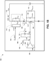
- the leak detection component 109 may measure the leakage current utilizing a capacitor 130, as illustrated by Fig. 1B .
- the capacitor 130 is connected to the solid state device 102 in parallel.
- switch 112 is closed (e.g., switch 112 is normally closed), the load 114 is disabled, and the device 102 is opened. In this way, the capacitor 130 is charged up to Vbattery. Then, the switch 112 is opened and the test voltage 118 is applied to the gate of the solid state device 102.
- a discharge rate of the capacitor 130 is proportional to the leakage current of the solid state device 102.
- an external source is used to charge the capacitor 103 or a current source may feed into a pin (e.g., pin Vfuse associated with voltage 116) while the load 114 is disabled and the switch 112 is opened.
- the leak detection component 109 measures a rate of change of a charge of the capacitor 130 over time to determine whether the rate of change of the charge of the capacitor 130 exceeds a threshold. The larger the rate of change of the charge of the capacitor 130, the larger the leakage current of the solid state device 102.
- the leak detection component 109 determines that the solid state device 102 is operating in a non-degraded operating state. If the rate of change of the charge of the capacitor 130 exceeds the threshold, then the leak detection component 109 determines that the solid state device 102 is operating in a degraded operating state.
- the leak detection component 109 may utilize other components and/or functionality than the capacitor 130 for measuring the leakage current of the solid state device 102.
- the leak detection component 109 utilizes a voltage source 140 as part of the test sequence for measuring the leakage current, as illustrated by Fig. 1C .
- the voltage source 140 may be an independent voltage source from other voltage sources of the apparatus 100 such as the voltage source 110.
- the leak detection component 109 utilizes a current source 150 as part of the test sequence for measuring the leakage current, as illustrated by Fig. 1D .
- the current source 150 may apply a current to a drain potential of a drain of the solid state device 102.
- Fig. 2 illustrates a method 200 for detecting leakage current of the solid state device 102.
- the solid state device 102 is turned on using the device enable signal 126.
- the device enable signal 126 causes the gate driver 104 to apply a voltage to the gate of the solid state device 102. The voltage is equal to or greater than the threshold voltage Vth of the solid state device 102. This causes the solid state device 102 to turn on.
- the solid state device 102 is turned on while the switch 112 is on (e.g., closed so that the voltage source 110 is connected to the load 114 and/or the solid state device 102).
- the load 114 is turned on using the load enable signal 124. In this way, the switch 112 is closed, and the solid state device 102 and the load 114 are turned on into an operational state.
- the device enable signal 126 is disabled to turn off the solid state device 102.
- the device enable signal 126 is an input into the gate driver 104 in order to control the gate driver 104.
- Disabling the device enable signal 126 triggers the gate driver 104 to stop applying the voltage, greater than the threshold voltage Vth, to the gate of the solid state device 102, thus turning off the solid state device 102.
- the gate driver 104 provides an off-level gate driver signal to the solid state device 102.
- the switch 112 is turned off to interrupt the supply of power to the solid state device 102.
- the switch is turned off (opened) in order to interrupt the supply of power from the voltage source 110 through the load 114 to the source of the solid state device 102.
- the test sequence triggers the test circuitry 108 to apply the test voltage 118 to the gate of the solid state device 102.
- the test sequence is initiated by applying the test voltage 118 to the gate of the solid state device 102 using the test circuitry 108.
- the test voltage 118 is less than the threshold voltage Vth such that if the solid state device 102 is operating in a non-degraded operating state (e.g., experiencing little to no threshold voltage Vth drift), then the solid state device 102 will not turn on and will not generate a large leakage current.
- the test sequence of the test voltage 118 being applied to the gate of the solid state device 102 and the leak detection component 109 determining a leakage current inducted by the test voltage 118 is performed in-situ when the apparatus 100 is deployed and operational (e.g., during a power up/down sequence of a vehicle boardnet of a vehicle).
- the test voltage 118 is applied to the gate of the solid state device 102 while the solid state device 102 is in an off state where the gate driver 104 is not applying the voltage greater than the threshold voltage Vth to the gate of the solid state device 102.
- the leak detection component 109 may generate a warning signal (e.g., turn on or blink a warning light of the apparatus 100, display an alert on a display of the apparatus 100, transmit the warning signal to a remote device or computer to notify a user, etc.).
- a warning signal e.g., turn on or blink a warning light of the apparatus 100, display an alert on a display of the apparatus 100, transmit the warning signal to a remote device or computer to notify a user, etc.
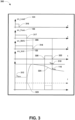
- Fig. 3 illustrates a timing diagram 300 associated with solid state device leak detection.
- the x-axis represents time during which the test sequence may be performed.
- the load enable signal 124 is initially enabled (high) so that the load 114 is on and operational.
- the device enable signal 126 is also initially enabled (high) so that the gate driver 104 applies a voltage to the gate of the solid state device 102.
- the voltage applied to the gate of the solid state device 102 is equal to or larger than the threshold voltage Vth 323 of the solid state device 102 (e.g., greater than 3.5V, 4.5V, or some other threshold voltage), and thus the solid state device 102 is on and operational.
- a switch enable signal 306, used to control the switch 112, is initially enabled (high) so that the switch 112 is on (closed).
- the load enable signal 124 is disabled (low) at a first point in time 316 to turn off the load 114.
- the device enable signal 126 is disabled (low) at a second point in time 317 to turn off the solid state device 102 by controlling the gate driver 104 to stop applying the voltage to the gate of the solid state device 102.
- the switch enable signal 306 is disabled (low) at a third point in time 318 so that the switch 112 is off (opened).
- the switch 112 may be turned off once the voltage 116 has reached a battery voltage 310 of the voltage source 110.
- Fig. 4 illustrates a diagram 400 depicting various voltage threshold drifts of the solid state device 102.
- the x-axis 404 represents voltage, such as the threshold voltage Vth 406 of the solid state device 102 and a gate-source voltage bias 408 of the solid state device 102.
- the y-axis 402 represents current from the solid state device 102, such as leakage current produced before a voltage applied to the gate of the solid state device 102 reaches the threshold voltage Vth 406.
- a current curve 410 represents current from the solid state device 102 if the solid state device is operating in a non-degraded operating state. The current curve 410 shows that there is little to no leakage current before the voltage applied to the gate reaches the threshold voltage Vth 406. Once the threshold voltage Vth 406 is reached, then current from the solid state device 102 increases because the solid state device 102 is on and operational.
- the current curve 412 illustrates how leakage current from the solid state device 102 occurs before the threshold voltage Vth 406 is reached, which is indicative of a leakage current due to drift in the threshold voltage Vth 406.
- Current curve 414 illustrates critical drift in the threshold voltage Vth 406 where there is leakage current well before the threshold voltage Vth 406 is reached.
- Current curve 416 illustrates very critical drift in the threshold voltage Vth 406 where the solid state device 102 may not even be able to turn off and there is significant leakage current while the solid state device 102 is supposed to be off.
- the techniques described herein are capable of detecting these leakage currents and voltage threshold drifts during operation of the solid state device 102 in order to provide early detection and warning of imminent or potential future failures.
- An embodiment of the presently disclosed techniques comprises an apparatus.
- the apparatus comprises a solid state device; a switch in series with the solid state device; a leak detection component connected to the solid state device; and a gate driver configured to drive a gate of the solid state device, wherein the gate driver comprises test circuitry configured to apply a test voltage to the gate of the solid state device, wherein the test voltage is less than a threshold voltage of the solid state device, and wherein a leakage current of the solid state device is detected by the leak detection component.
- a signal is generated based upon the leakage current of the solid state device to indicate whether the solid state device is operating in a degraded operating state or a non-degraded operating state.
- a drift of the threshold voltage of the solid state device is determined based upon the leakage current.
- the test voltage is applied to the gate of the solid state device and the leakage current is determined in-situ during operation of the apparatus and the solid state device.
- the leak detection component comprises a capacitor connected in parallel to the solid state device, wherein the capacitor is charged when the switch is closed, and wherein the leak detection component detects the leakage current based upon a rate of a change of a charge of the capacitor over a period of time exceeding a threshold when the switch is open.
- the test voltage is applied to the gate of the solid state device while the solid state device is in an off state.
- the test circuitry comprises a series switch for the gate.
- the test circuitry comprises a voltage source that produces the test voltage.
- the apparatus is a circuit breaker or e-Fuse.
- An embodiment of the presently disclosed techniques comprises a method.
- the method comprises turning on a solid state device using a device enable signal and turning on a load using a load enable signal while a switch is on; disabling the load enable signal to turn off the load; disabling the device enable signal to turn off the solid state device; turning off the switch to interrupt supply of power to the solid state device; in response to turning off the switch, initiate a test sequence by applying a test voltage to a gate of the solid state device; measuring a leakage current of the solid state device; and determining whether the solid state device is operating in a degraded operating state based upon the leakage current.
- the initiating the test sequence comprises measuring a rate of a change of a charge of a capacitor over time, wherein the capacitor is connected to the solid state device in parallel; and determining whether the solid state device is operating in the degraded operating state based upon the rate of the change of the charge of the capacitor over time.
- the initiating the test sequence comprises determining the leakage current of the solid state device based upon a rate of a change of a charge of a capacitor over time, wherein the capacitor is connected to the solid state device in parallel; and determining whether the solid state device is operating in the degraded operating state based upon the leakage current.
- the initiating the test sequence comprises applying, by test circuitry integrated into a gate driver, the test voltage to the gate of the solid state device, wherein the test voltage is less than a threshold voltage of the solid state device; and determining whether the solid state device is operating in the degraded operating state based upon the leakage current induced by the test voltage.
- the method comprises in response to determining that the solid state device is operating in the degraded operating state, generating a warning signal.
- the initiating the test sequence comprises applying, by test circuitry integrated into a gate driver, the test voltage to the gate of the solid state device while the solid state device is in an off state.
- An embodiment of the presently disclosed techniques comprises an apparatus.
- the apparatus comprises a gate driver connected to and configured to drive a gate of a solid state device in series with a switch, wherein the solid state device is in parallel with a capacitor charged by an auxiliary voltage when the switch is open, and wherein the gate driver comprises test circuitry configured to: apply a test voltage to the gate of the solid state device, wherein a rate of change of a charge of the capacitor over time is determined while the test voltage is applied to the gate of the solid state device, and wherein the rate of change of the charge of the capacitor over time is evaluated against a threshold rate change to determine whether the solid state device is operating in a degraded operating state.
- the rate of change of the charge of the capacitor over time is used to determine a leakage current of the solid state device, and wherein the leakage current is used to determine whether the solid state device is operating in the degraded operating state.
- the degraded operating state corresponds to a drift in a threshold voltage of the solid state device.
- the test circuitry is configured to perform a test sequence to determine whether the solid state device is operating in the degraded operating state, wherein the test sequence includes charging the capacitor, turning on the switch, applying the test voltage to the gate of the solid state device, and measuring the auxiliary voltage across the switch to identify the rate of change of the charge of the capacitor over time.
- the terms “component,” “module,” “system”, “interface”, and the like are generally intended to refer to a computer-related entity, either hardware, a combination of hardware and software, software, or software in execution.
- One or more components may be localized on one computer and/or distributed between two or more computers.
- the claimed subject matter may be implemented as a method, apparatus, or article of manufacture using standard programming and/or engineering techniques to produce software, firmware, hardware, or any combination thereof to control a computer to implement the disclosed subject matter.
- article of manufacture as used herein is intended to encompass a computer program accessible from any computer-readable device, carrier, or media.
- one or more of the operations described may constitute computer readable instructions stored on one or more computer readable media, which if executed by a computing device, will cause the computing device to perform the operations described.
- the order in which some or all of the operations are described should not be construed as to imply that these operations are necessarily order dependent. Alternative ordering will be appreciated by one skilled in the art having the benefit of this description. Further, it will be understood that not all operations are necessarily present in each embodiment provided herein.
- any aspect or design described herein as an "example” is not necessarily to be construed as advantageous over other aspects or designs. Rather, use of the word “example” is intended to present one possible aspect and/or implementation that may pertain to the techniques presented herein. Such examples are not necessary for such techniques or intended to be limiting. Various embodiments of such techniques may include such an example, alone or in combination with other features, and/or may vary and/or omit the illustrated example.
- first,” “second,” or the like are not intended to imply a temporal aspect, a spatial aspect, an ordering, etc. Rather, such terms are merely used as identifiers, names, etc. for features, elements, items, etc.
- a first element and a second element generally correspond to element A and element B or two different or two identical elements or the same element.
Landscapes
- Physics & Mathematics (AREA)
- General Physics & Mathematics (AREA)
- Engineering & Computer Science (AREA)
- Microelectronics & Electronic Packaging (AREA)
- Environmental & Geological Engineering (AREA)
- General Engineering & Computer Science (AREA)
- Health & Medical Sciences (AREA)
- Toxicology (AREA)
- Computer Hardware Design (AREA)
- Power Engineering (AREA)
- Testing Of Individual Semiconductor Devices (AREA)
- Investigating Or Analyzing Materials By The Use Of Electric Means (AREA)
Abstract
Description
- The present disclosure relates to the field of current leak detection for solid state devices.
- Solid state devices, such as solid state switches, are used in various applications such as in circuit breakers, e-Fuses, etc. In these types of applications, the solid state devices may remain in the same state for extended periods of time. For example, a solid state device of a circuit breaker may remain in an on state where the solid state device is conducting for years. The solid state device will turn off and close to stop conducting if there is an abnormal condition such as an overload or short circuit. Unfortunately, there is no way to test the solid state device to see if the solid state device is operating correctly and will be able to completely turn off in the event of the abnormal condition. This can result in catastrophic failures and damage.
- This Summary is provided to introduce a selection of concepts in a simplified form that are further described below in the Detailed Description. This Summary is not intended to identify key factors or essential features of the claimed subject matter, nor is it intended to be used to limit the scope of the claimed subject matter.
- In an embodiment of the techniques presented herein, an apparatus is provided. The apparatus comprises a solid state device. A switch is connected in series with the solid state device. A leak detection component is connected to the solid state device. A gate driver is configured to drive a gate of the solid state device. The gate driver comprises test circuitry configured to apply a test voltage to the gate of the solid state device. The test voltage is less than a threshold voltage of the solid state device. A leakage current of the solid state device is detected by the leak detection component.
- In an embodiment of the techniques presented herein, a method is provided. The method includes turning on a solid state device using a device enable signal and turning on a load using a load enable signal while a switch is on. The load enable signal is disabled to turn off the load. The device enable signal is disabled to turn off the solid state device. The switch is turned off to interrupt supply of power to the solid state device. In response to turning off the switch, a test sequence is initiated by applying a test voltage to a gate of the solid state device. A leakage current of the solid state device is measured. A determination is made as to whether the solid state device is operating in a degraded operating state based upon the leakage current.
- In an embodiment of the techniques presented herein, an apparatus is provided. The apparatus comprises a means for turning on a solid state device using a device enable signal and turning on a load using a load enable signal while a switch is on. The apparatus comprises a means for disabling the load enable signal to turn off the load. The apparatus comprises a means for disabling the device enable signal to turn off the solid state device. The apparatus comprises a means for turning off the switch to interrupt supply of power to the solid state device. The apparatus comprises a means for initiating a test sequence by applying a test voltage to a gate of the solid state device in response to turning off the switch. The apparatus comprises a means for measuring a leakage current of the solid state device. The apparatus comprises a means for determining whether the solid state device is operating in a degraded operating state based upon the leakage current
- In an embodiment of the techniques presented herein, an apparatus is provided. The apparatus comprises a gate driver connected to and configured to drive a gate of a solid state device in series with a switch. The solid state device is in parallel with a capacitor charged by an auxiliary voltage when the switch is open. The gate driver comprises test circuitry configured to apply a test voltage to the gate of the solid state device. A rate of change of a charge of the capacitor over time is determined while the test voltage is applied to the gate of the solid state device. The rate of change of the charge of the capacitor over time is evaluated against a threshold rate change to determine whether the solid state device is operating in a degraded operating state.
- To the accomplishment of the foregoing and related ends, the following description and annexed drawings set forth certain illustrative aspects and implementations. These are indicative of but a few of the various ways in which one or more aspects may be employed. Other aspects, advantages, and novel features of the disclosure will become apparent from the following detailed description when considered in conjunction with the annexed drawings.
-
Fig. 1A is a component block diagram illustrating a leak detection component for current leak detection of a solid state device in accordance with at least some of the techniques presented herein. -
Fig. 1B is a component block diagram illustrating a leak detection component for current leak detection of a solid state device using a capacitor in accordance with at least some of the techniques presented herein. -
Fig. 1C is a component block diagram illustrating a leak detection component for current leak detection of a solid state device using a voltage source in accordance with at least some of the techniques presented herein. -
Fig. 1D is a component block diagram illustrating a leak detection component for current leak detection of a solid state device using a current source in accordance with at least some of the techniques presented herein. -
Fig. 2 is an illustration of an example method for current leak detection of a solid state device in accordance with at least some of the techniques presented herein. -
Fig. 3 is an illustration of a timing diagram associated with solid state device leak detection in accordance with at least some of the techniques presented herein. -
Fig. 4 is an illustration of voltage threshold drifts of a solid state device in accordance with at least some of the techniques presented herein. - The claimed subject matter is now described with reference to the drawings, wherein like reference numerals are used to refer to like elements throughout. In the following description, for purposes of explanation, numerous specific details are set forth in order to provide a thorough understanding of the claimed subject matter. It may be evident, however, that the claimed subject matter may be practiced without these specific details. In other instances, well-known structures and devices are shown in block diagram form in order to facilitate describing the claimed subject matter.
- Various devices, such as e-Fuses and circuit breakers, may utilize solid state devices that operate in either an on state or an off state. These solid state devices may comprise solid state switches, metal-oxide-semiconductor field-effect transistors (MOSFETs), etc. A solid state device may transition from one of the states to another state based upon a voltage applied to a gate of the solid state device. Once the voltage of the gate reaches a threshold voltage Vth, then the solid state device may change states, such as where the solid state device is turned on and starts conducting. In certain applications, the solid state device may remain in a particular state for an extended period of time. This period of time could be years, such as where a solid state device of a circuit breaker is in an on state until an abnormal condition of an electric supply network occurs such as an overload or short circuit. Because the solid state device remains in one state for such a long period of time, there is no way to verify that the solid state device is operating correctly and will be able to transition states when needed such as to safely turn off when the abnormal condition occurs. This can lead to catastrophic failures and damage.
- The health and operability of the solid state device may deteriorate over time due to various reasons such as stress on the solid state device. One issue that can occur is that the threshold voltage Vth of the gate can drift over time, which can lead to excessive leakage current, leakage current due to a drain source on resistance (RDSon) being too low, and/or failure where the solid state device cannot switch states such as to turn off safely. As the threshold voltage Vth drifts towards 0, the solid state device may not even be able to turn off. High leakage currents due to this drift causes health deterioration of the apparatus comprising the solid state device, such as where there is always current flowing through the solid state device to a secondary side of the apparatus. This could lead to a high voltage condition on the secondary side that should otherwise be turned off. If the solid state device cannot completely shut off, then the solid state device will operate similar to a current source and deliver a significant amount of current (e.g., 10 to 100 milliamps) that can cause overheating and failure due to damage from thermal overstress behavior. The drift of the threshold voltage Vth can occur over a long period of time, and thus the leakage current may slowly increase over time. There is currently no ability to detect this slow drift and leakage current increase in-situ during operation of the apparatus comprising the solid state device.
- In order to improve the ability to monitor the health of solid state devices in-situ during operation of apparatuses comprising the solid state devices, a leak detection component and leak detection technique are provided. The leak detection component is capable of testing and monitoring a solid state device of an apparatus during operation of the apparatus in order to detect imminent or future failure of the solid state device. The leak detection component is capable of identifying drift of the threshold voltage Vth of the solid state device based upon a leakage current of the solid state device measured by the leak detection component. The leakage current is detected during operation of the apparatus (e.g., while the circuit breaker or e-Fuse is installed and operational, as opposed to in a test lab environment) by the leak detection component by applying a test voltage to a gate of the solid state device. The leak detection component detects a leakage current resulting from the test voltage being applied to the gate of the solid state device. The test voltage is less than the threshold voltage Vth of the
solid state device 102 such that increased leakage current will be detected if the solid state device is operating in a degraded operating state (e.g., leakage current larger than a nanoampere range of normal/expected leakage current of a non-degraded device) due to drift of the threshold voltage Vth (e.g., the threshold voltage Vth has drifted down to a smaller value than normal). Otherwise, the test voltage would not be enough voltage to cause the solid state device, operating in a non-degraded operating state, to turn on and conduct current through the solid state device. If the solid state device is operating in the degraded operating state, then various actions can be performed such as generating a warning signal of the degraded operating state (e.g., blinking a light, displaying a message, transmitting a message to a remote device, etc.). -
Fig. 1A illustrates aleak detection component 109 configured to dynamically monitor the operating state and health of a solid state device 102 (e.g., a device under test (DUT)) of anapparatus 100. Theapparatus 100 comprises avoltage source 110 that is connected to aswitch 112. In some embodiments where theapparatus 100 is an e-Fuse being used for a DC breaker application, theswitch 112 is a battery main switch that electrically connects and disconnects thevoltage source 110 from other components of theapparatus 100 such as thesolid state device 102. In some embodiments, theswitch 112 may be connected in series with thesolid state device 102 so that power from thevoltage source 110 is supplied to the solid state device 102 (e.g., to a source of the solid state device 102) when theswitch 112 is on (closed). - The
apparatus 100 comprises aload 114 connected in series to theswitch 112 and thesolid state device 102. It may be appreciated that in some embodiments, theload 114 is represented by a resistance Rdisc and capacitance Cbyp for simplicity, but may comprise various components, circuitry, hardware, and/or software. When theload 114 is on and in an operating state, an auxiliarycurrent laux 120 and a voltage 116 (e.g., Vfuse) may be applied to the source of thesolid state device 102 that is connected in series to theload 114. Theload 114 may be in an operational state (on) or a non-operational (off) based upon a load enable signal 124 (e.g., a signal generated by software to turn on or off the load 114). Thesignal 124 may be used to control acontrollable portion 115 of theload 114, such as an inverter circuit. In some embodiments, a discharge circuit of the load 114 (e.g., Rdisc and Cbyp) may be permanently connected. In some embodiments, theload 114 may generate the auxiliarycurrent laux 120 and thevoltage 116 when the load enablesignal 124 is enabled to turn on theload 114 and theswitch 112 is closed so that theload 114 is connected to thevoltage source 110. - A gate driver 104 (GDU) may be connected to the gate of the
solid state device 102. Thegate driver 104 may be configured to drive the gate of thesolid state device 102 by applying a voltage to thesolid state device 102 in order to operate thesolid state device 102. When thegate driver 104 applies a voltage equal to or greater than the threshold voltage Vth of thesolid state device 102, then thesolid state device 102 will turn on into an operational state. A device enablesignal 126 may be used to control thegate driver 104 to turn on or off thesolid state device 102. When thesolid state device 102 is to be turned on, the device enablesignal 126 causes thegate driver 104 to apply the voltage, equal to or greater than the threshold voltage Vth of thesolid state device 102, to the gate of thesolid state device 102. When thesolid state device 102 is to be turned off, the device enablesignal 126 is disabled to cause thegate driver 104 to stop applying the voltage to the gate of thesolid state device 102. - If the threshold voltage Vth of the
solid state device 102 drifts over time to lower voltage values, then thesolid state device 102 will produce significant leakage current when thesolid state device 102 is supposed to be in an off state even to the point of where thesolid state device 102 is not able to fully turn off by applying a normally applied off-level voltage via thegate driver 104. This can cause catastrophic failure and damage to theapparatus 100, such as where a circuit breaker is unable to turn off in the event of a short circuit or other abnormal condition. In order to detect drift of the threshold voltage Vth and/or leakage current of thesolid state device 102 during operation of theapparatus 100, theleak detection component 109 in combination with a dedicated gate stimulus circuit (e.g., test circuitry 108) is used to detect these indicators of degraded performance and potential failure of thesolid state device 102. - The
leak detection component 109 may be connected to thesolid state device 102. In some embodiments, theleak detection component 109 is connected in parallel with thesolid state device 102. In some embodiments, theleak detection component 109 is connected to a source and a drain of thesolid state device 102. In some embodiments, a leak detection component may be implemented as a current measurement device in series with thesolid state device 102. Theleak detection component 109 is configured to measure a leakage current of thesolid state device 102 when a test voltage is applied to the gate of thesolid state device 102 during a test sequence. The test sequence is used to test the health of thesolid state device 102 for determining whether thesolid state device 102 is operating in a non-degraded operating state or degraded operating state. Details of the test sequence are further described in conjunction with themethod 200 ofFig. 2 . - As part of performing the test sequence, the
apparatus 100 includestest circuitry 108 configured to apply atest voltage 118 to the gate of thesolid state device 102. In some embodiments, thetest circuitry 108 is integrated into thegate driver 104. Thetest circuitry 108 is controlled by a test enablesignal 122. In response to the test enablesignal 122 indicating that the test sequence is to be initiated (e.g., a threshold amount of time has occurred since a prior test sequence was performed), thetest circuitry 108 closes aseries switch 123 that is in series between atest voltage source 119 and the gate of thesolid state device 102. Closing theseries switch 123 connects thetest voltage source 119 to the gate of thesolid state device 102 so that that thetest voltage 118 is applied to the gate of thesolid state device 102. Thetest voltage 118 is less than the threshold voltage Vth. In this way, thesolid state device 102 will not turn on from thetest voltage 118 being applied to the gate of thesolid state device 102 if thesolid state device 102 is operating in a non-degraded operating state and has not experienced significant drift of the threshold voltage Vth. In some embodiments, thetest voltage 118 is applied to the gate of thesolid state device 102 while thesolid state device 102 is in an off state where thegate driver 104 is not applying a voltage to the gate of thesolid state device 102. - As part of performing the test sequence, the
leak detection component 109 measures the leakage current output through thesolid state device 102 while thetest voltage 118 is applied to the gate of thesolid state device 102. In some embodiments, theleak detection component 109 may measure the leakage current utilizing acapacitor 130, as illustrated byFig. 1B . Thecapacitor 130 is connected to thesolid state device 102 in parallel. As part of starting the test sequence,switch 112 is closed (e.g.,switch 112 is normally closed), theload 114 is disabled, and thedevice 102 is opened. In this way, thecapacitor 130 is charged up to Vbattery. Then, theswitch 112 is opened and thetest voltage 118 is applied to the gate of thesolid state device 102. Because there is no current feed from Vbattery due to theswitch 112 being opened, a discharge rate of thecapacitor 130 is proportional to the leakage current of thesolid state device 102. In some embodiments, an external source is used to charge the capacitor 103 or a current source may feed into a pin (e.g., pin Vfuse associated with voltage 116) while theload 114 is disabled and theswitch 112 is opened. As thetest voltage 118 is applied to the gate of thesolid state device 102, theleak detection component 109 measures a rate of change of a charge of thecapacitor 130 over time to determine whether the rate of change of the charge of thecapacitor 130 exceeds a threshold. The larger the rate of change of the charge of thecapacitor 130, the larger the leakage current of thesolid state device 102. The larger the leakage current of thesolid state device 102, the larger the drift of the threshold voltage Vth. The larger the rate of change of the charge of the capacitor 130 (e.g., the rate of change of the charge of thecapacitor 130 exceeding the threshold) and the larger the leakage current and the larger the drift of the threshold voltage Vth, then the more thesolid state device 102 is operating in a degraded operating state. In some embodiments of performing the test sequence, the test sequence may include charging thecapacitor 130, turning on theswitch 112, and then measuring thevoltage 116 across theswitch 112 to identify the rate of change of the charged of thecapacitor 130 over time. - If the rate of change of the charge of the
capacitor 130 does not exceed the threshold, then theleak detection component 109 determines that thesolid state device 102 is operating in a non-degraded operating state. If the rate of change of the charge of thecapacitor 130 exceeds the threshold, then theleak detection component 109 determines that thesolid state device 102 is operating in a degraded operating state. If theleak detection component 109 determines that thesolid state device 102 is operating in a degraded operating state, then theleak detection component 109 may generate a signal, such as a warning signal that thesolid state device 102 is unhealthy, operating in the degraded operating state, and/or should be replaced (e.g., the signal may cause a light on theapparatus 100 to turn on, a message to be displayed on theapparatus 100, or a message to be transmitted to a remote device over a communication network). - It may be appreciated that the
leak detection component 109 may utilize other components and/or functionality than thecapacitor 130 for measuring the leakage current of thesolid state device 102. In some embodiments, theleak detection component 109 utilizes avoltage source 140 as part of the test sequence for measuring the leakage current, as illustrated byFig. 1C . Thevoltage source 140 may be an independent voltage source from other voltage sources of theapparatus 100 such as thevoltage source 110. In some embodiments, theleak detection component 109 utilizes acurrent source 150 as part of the test sequence for measuring the leakage current, as illustrated byFig. 1D . Thecurrent source 150 may apply a current to a drain potential of a drain of thesolid state device 102. Instead of applying thetest voltage 118 as part of the test sequence, a current through thesolid state device 102 is measured to determine the leakage current of thesolid state device 102. In some embodiments, a leak detection component may be implemented as a current measurement device in series with thesolid state device 102. -
Fig. 2 illustrates amethod 200 for detecting leakage current of thesolid state device 102. Duringoperation 202 ofmethod 200, thesolid state device 102 is turned on using the device enablesignal 126. In some embodiments, the device enablesignal 126 causes thegate driver 104 to apply a voltage to the gate of thesolid state device 102. The voltage is equal to or greater than the threshold voltage Vth of thesolid state device 102. This causes thesolid state device 102 to turn on. In some embodiments, thesolid state device 102 is turned on while theswitch 112 is on (e.g., closed so that thevoltage source 110 is connected to theload 114 and/or the solid state device 102). In some embodiments, theload 114 is turned on using the load enablesignal 124. In this way, theswitch 112 is closed, and thesolid state device 102 and theload 114 are turned on into an operational state. - The
leak detection component 109 may determine that a test sequence is to be initiated to determine whether thesolid state device 102 is operating in a non-degraded operating state or a degraded operating state (e.g., a threshold amount of time has passed since a prior test sequence was performed). Accordingly, duringoperation 204 ofmethod 200, the load enablesignal 124 is disabled in order to turn off theload 114. In this way, theload 114 is not drawing power, such as from thevoltage source 110, while off. In some embodiments, theload 114 is turned off while theswitch 112 is still on (closed). - During
operation 206 ofmethod 200, the device enablesignal 126 is disabled to turn off thesolid state device 102. In particular, the device enablesignal 126 is an input into thegate driver 104 in order to control thegate driver 104. Disabling the device enablesignal 126 triggers thegate driver 104 to stop applying the voltage, greater than the threshold voltage Vth, to the gate of thesolid state device 102, thus turning off thesolid state device 102. In particular, thegate driver 104 provides an off-level gate driver signal to thesolid state device 102. - During
operation 208 ofmethod 200, theswitch 112 is turned off to interrupt the supply of power to thesolid state device 102. In some embodiments, the switch is turned off (opened) in order to interrupt the supply of power from thevoltage source 110 through theload 114 to the source of thesolid state device 102. Once the switch is turned off, and theload 114 and thesolid state device 102 are turned off, the test sequence triggers thetest circuitry 108 to apply thetest voltage 118 to the gate of thesolid state device 102. - During
operation 210 ofmethod 200, the test sequence is initiated by applying thetest voltage 118 to the gate of thesolid state device 102 using thetest circuitry 108. Thetest voltage 118 is less than the threshold voltage Vth such that if thesolid state device 102 is operating in a non-degraded operating state (e.g., experiencing little to no threshold voltage Vth drift), then thesolid state device 102 will not turn on and will not generate a large leakage current. In some embodiments, the test sequence of thetest voltage 118 being applied to the gate of thesolid state device 102 and theleak detection component 109 determining a leakage current inducted by thetest voltage 118 is performed in-situ when theapparatus 100 is deployed and operational (e.g., during a power up/down sequence of a vehicle boardnet of a vehicle). In some embodiments, thetest voltage 118 is applied to the gate of thesolid state device 102 while thesolid state device 102 is in an off state where thegate driver 104 is not applying the voltage greater than the threshold voltage Vth to the gate of thesolid state device 102. - During
operation 212 ofmethod 200, theleak detection component 109 measures the leakage current from thesolid state device 102. The leakage current may be induced by thetest voltage 118 being applied to the gate of thesolid state device 102. Various techniques may be used to measure the leakage current or other operational properties of thesolid state device 102, such as through the use of thecapacitor 130 ofFig. 1B , thevoltage source 140 ofFig. 1C , thecurrent source 150 ofFig. 1D , etc. In some embodiments of using thecapacitor 130, theleak detection component 109 measures a rate of change of a charge of thecapacitor 130 over time. The leakage detection components determines the leakage current based upon the rate of change of the charge of thecapacitor 130 over time. - During
operation 214 ofmethod 200, theleak detection component 109 determines whether thesolid state device 102 is operating in a degraded operating state or a non-degraded operation state based upon the leakage current of thesolid state device 102 and/or the rate of change of the charge of thecapacitor 130 over time. If theleak detection component 109 determines that the solid state device is in the degraded operating state (e.g., the leakage current exceeds a threshold; the threshold voltage Vth has drifted by 1V, 2V, or some other voltage such as where a 3.5V drift that would be catastrophic if the threshold voltage Vth is 3.5V), then theleak detection component 109 may generate a warning signal (e.g., turn on or blink a warning light of theapparatus 100, display an alert on a display of theapparatus 100, transmit the warning signal to a remote device or computer to notify a user, etc.). -
Fig. 3 illustrates a timing diagram 300 associated with solid state device leak detection. The x-axis represents time during which the test sequence may be performed. The load enablesignal 124 is initially enabled (high) so that theload 114 is on and operational. The device enablesignal 126 is also initially enabled (high) so that thegate driver 104 applies a voltage to the gate of thesolid state device 102. The voltage applied to the gate of thesolid state device 102 is equal to or larger than thethreshold voltage Vth 323 of the solid state device 102 (e.g., greater than 3.5V, 4.5V, or some other threshold voltage), and thus thesolid state device 102 is on and operational. A switch enablesignal 306, used to control theswitch 112, is initially enabled (high) so that theswitch 112 is on (closed). - A determination is made that the test sequence is to be performed. Accordingly, the load enable
signal 124 is disabled (low) at a first point intime 316 to turn off theload 114. The device enablesignal 126 is disabled (low) at a second point intime 317 to turn off thesolid state device 102 by controlling thegate driver 104 to stop applying the voltage to the gate of thesolid state device 102. The switch enablesignal 306 is disabled (low) at a third point intime 318 so that theswitch 112 is off (opened). Theswitch 112 may be turned off once thevoltage 116 has reached abattery voltage 310 of thevoltage source 110. - At a fourth point in
time 320, the test enablesignal 122 is enabled (high) to cause thetest circuitry 108 to apply thetest voltage 118 to the gate of thesolid state device 102, which has agate voltage 312. A rate ofchange 324 of a charge of thecapacitor 130 is measured while thetest voltage 118 is applied to the gate of thesolid state device 102 in order to determine an increase in leakage current of thesolid state device 102 from thetest voltage 118 being applied to the gate of thesolid state device 102. Once the leakage current and/or a drift of the threshold voltage Vth is determined, the test enablesignal 122 is disabled (low) at a fifth point intime 322 to complete the test sequence. -
Fig. 4 illustrates a diagram 400 depicting various voltage threshold drifts of thesolid state device 102. Thex-axis 404 represents voltage, such as thethreshold voltage Vth 406 of thesolid state device 102 and a gate-source voltage bias 408 of thesolid state device 102. The y-axis 402 represents current from thesolid state device 102, such as leakage current produced before a voltage applied to the gate of thesolid state device 102 reaches thethreshold voltage Vth 406. Acurrent curve 410 represents current from thesolid state device 102 if the solid state device is operating in a non-degraded operating state. Thecurrent curve 410 shows that there is little to no leakage current before the voltage applied to the gate reaches thethreshold voltage Vth 406. Once thethreshold voltage Vth 406 is reached, then current from thesolid state device 102 increases because thesolid state device 102 is on and operational. - As the
solid state device 102 experiences voltage threshold drift, leakage current from thesolid state device 102 will occur before thethreshold voltage Vth 406 is reached. Thecurrent curve 412 illustrates how leakage current from thesolid state device 102 occurs before thethreshold voltage Vth 406 is reached, which is indicative of a leakage current due to drift in thethreshold voltage Vth 406.Current curve 414 illustrates critical drift in thethreshold voltage Vth 406 where there is leakage current well before thethreshold voltage Vth 406 is reached.Current curve 416 illustrates very critical drift in thethreshold voltage Vth 406 where thesolid state device 102 may not even be able to turn off and there is significant leakage current while thesolid state device 102 is supposed to be off. As previously discussed, the techniques described herein are capable of detecting these leakage currents and voltage threshold drifts during operation of thesolid state device 102 in order to provide early detection and warning of imminent or potential future failures. - An embodiment of the presently disclosed techniques comprises an apparatus. The apparatus comprises a solid state device; a switch in series with the solid state device; a leak detection component connected to the solid state device; and a gate driver configured to drive a gate of the solid state device, wherein the gate driver comprises test circuitry configured to apply a test voltage to the gate of the solid state device, wherein the test voltage is less than a threshold voltage of the solid state device, and wherein a leakage current of the solid state device is detected by the leak detection component.
- According to some embodiments, a signal is generated based upon the leakage current of the solid state device to indicate whether the solid state device is operating in a degraded operating state or a non-degraded operating state.
- According to some embodiments, a drift of the threshold voltage of the solid state device is determined based upon the leakage current.
- According to some embodiments, the test voltage is applied to the gate of the solid state device and the leakage current is determined in-situ during operation of the apparatus and the solid state device.
- According to some embodiments, the leak detection component comprises a capacitor connected in parallel to the solid state device, wherein the capacitor is charged when the switch is closed, and wherein the leak detection component detects the leakage current based upon a rate of a change of a charge of the capacitor over a period of time exceeding a threshold when the switch is open.
- According to some embodiments, the test voltage is applied to the gate of the solid state device while the solid state device is in an off state.
- According to some embodiments, the test circuitry comprises a series switch for the gate.
- According to some embodiments, the test circuitry comprises a voltage source that produces the test voltage.
- According to some embodiments, the apparatus is a circuit breaker or e-Fuse.
- An embodiment of the presently disclosed techniques comprises a method. The method comprises turning on a solid state device using a device enable signal and turning on a load using a load enable signal while a switch is on; disabling the load enable signal to turn off the load; disabling the device enable signal to turn off the solid state device; turning off the switch to interrupt supply of power to the solid state device; in response to turning off the switch, initiate a test sequence by applying a test voltage to a gate of the solid state device; measuring a leakage current of the solid state device; and determining whether the solid state device is operating in a degraded operating state based upon the leakage current.
- According to some embodiments, the initiating the test sequence comprises measuring a rate of a change of a charge of a capacitor over time, wherein the capacitor is connected to the solid state device in parallel; and determining whether the solid state device is operating in the degraded operating state based upon the rate of the change of the charge of the capacitor over time.
- According to some embodiments, the initiating the test sequence comprises determining the leakage current of the solid state device based upon a rate of a change of a charge of a capacitor over time, wherein the capacitor is connected to the solid state device in parallel; and determining whether the solid state device is operating in the degraded operating state based upon the leakage current.
- According to some embodiments, the initiating the test sequence comprises applying, by test circuitry integrated into a gate driver, the test voltage to the gate of the solid state device, wherein the test voltage is less than a threshold voltage of the solid state device; and determining whether the solid state device is operating in the degraded operating state based upon the leakage current induced by the test voltage.
- According to some embodiments, the test sequence is performed in-situ during operation of an apparatus comprising the solid state device.
- According to some embodiments, the method comprises in response to determining that the solid state device is operating in the degraded operating state, generating a warning signal.
- According to some embodiments, the initiating the test sequence comprises applying, by test circuitry integrated into a gate driver, the test voltage to the gate of the solid state device while the solid state device is in an off state.
- An embodiment of the presently disclosed techniques comprises an apparatus. The apparatus comprises a gate driver connected to and configured to drive a gate of a solid state device in series with a switch, wherein the solid state device is in parallel with a capacitor charged by an auxiliary voltage when the switch is open, and wherein the gate driver comprises test circuitry configured to: apply a test voltage to the gate of the solid state device, wherein a rate of change of a charge of the capacitor over time is determined while the test voltage is applied to the gate of the solid state device, and wherein the rate of change of the charge of the capacitor over time is evaluated against a threshold rate change to determine whether the solid state device is operating in a degraded operating state.
- According to some embodiments, the rate of change of the charge of the capacitor over time is used to determine a leakage current of the solid state device, and wherein the leakage current is used to determine whether the solid state device is operating in the degraded operating state.
- According to some embodiments, the degraded operating state corresponds to a drift in a threshold voltage of the solid state device.
- According to some embodiments, the test circuitry is configured to perform a test sequence to determine whether the solid state device is operating in the degraded operating state, wherein the test sequence includes charging the capacitor, turning on the switch, applying the test voltage to the gate of the solid state device, and measuring the auxiliary voltage across the switch to identify the rate of change of the charge of the capacitor over time.
- Although the subject matter has been described in language specific to structural features and/or methodological acts, it is to be understood that the subject matter defined in the appended claims is not necessarily limited to the specific features or acts described above. Rather, the specific features and acts described above are disclosed as example forms of implementing the claims.
- As used in this application, the terms "component," "module," "system", "interface", and the like are generally intended to refer to a computer-related entity, either hardware, a combination of hardware and software, software, or software in execution. One or more components may be localized on one computer and/or distributed between two or more computers.
- Furthermore, the claimed subject matter may be implemented as a method, apparatus, or article of manufacture using standard programming and/or engineering techniques to produce software, firmware, hardware, or any combination thereof to control a computer to implement the disclosed subject matter. The term "article of manufacture" as used herein is intended to encompass a computer program accessible from any computer-readable device, carrier, or media. Of course, those skilled in the art will recognize many modifications may be made to this configuration without departing from the scope or spirit of the claimed subject matter.
- Various operations of embodiments are provided herein. In one embodiment, one or more of the operations described may constitute computer readable instructions stored on one or more computer readable media, which if executed by a computing device, will cause the computing device to perform the operations described. The order in which some or all of the operations are described should not be construed as to imply that these operations are necessarily order dependent. Alternative ordering will be appreciated by one skilled in the art having the benefit of this description. Further, it will be understood that not all operations are necessarily present in each embodiment provided herein.
- Any aspect or design described herein as an "example" is not necessarily to be construed as advantageous over other aspects or designs. Rather, use of the word "example" is intended to present one possible aspect and/or implementation that may pertain to the techniques presented herein. Such examples are not necessary for such techniques or intended to be limiting. Various embodiments of such techniques may include such an example, alone or in combination with other features, and/or may vary and/or omit the illustrated example.
- As used in this application, the term "or" is intended to mean an inclusive "or" rather than an exclusive "or". That is, unless specified otherwise, or clear from context, "X employs A or B" is intended to mean any of the natural inclusive permutations. That is, if X employs A; X employs B; or X employs both A and B, then "X employs A or B" is satisfied under any of the foregoing instances. In addition, the articles "a" and "an" as used in this application and the appended claims may generally be construed to mean "one or more" unless specified otherwise or clear from context to be directed to a singular form. Also, unless specified otherwise, "first," "second," or the like are not intended to imply a temporal aspect, a spatial aspect, an ordering, etc. Rather, such terms are merely used as identifiers, names, etc. for features, elements, items, etc. For example, a first element and a second element generally correspond to element A and element B or two different or two identical elements or the same element.
- Also, although the disclosure has been shown and described with respect to one or more implementations, equivalent alterations and modifications will occur to others skilled in the art based upon a reading and understanding of this specification and the annexed drawings. The disclosure includes all such modifications and alterations and is limited only by the scope of the following claims. In particular regard to the various functions performed by the above described components (e.g., elements, resources, etc.), the terms used to describe such components are intended to correspond, unless otherwise indicated, to any component which performs the specified function of the described component (e.g., that is functionally equivalent), even though not structurally equivalent to the disclosed structure which performs the function in the herein illustrated example implementations of the disclosure. In addition, while a particular feature of the disclosure may have been disclosed with respect to only one of several implementations, such feature may be combined with one or more other features of the other implementations as may be desired and advantageous for any given or particular application. Furthermore, to the extent that the terms "includes", "having", "has", "with", or variants thereof are used in either the detailed description or the claims, such terms are intended to be inclusive in a manner similar to the term "comprising."
Claims (15)
- An apparatus, comprising:a solid state device (102);a switch (112) in series with the solid state device (102);a leak detection component (109) connected to the solid state device (102); anda gate driver (104) configured to drive a gate of the solid state device (102), wherein the gate driver (104) comprises test circuitry (108) configured to apply a test voltage (118) to the gate of the solid state device (102), wherein the test voltage (118) is less than a threshold voltage of the solid state device (102), and wherein a leakage current of the solid state device (102) is detected by the leak detection component (108).
- The apparatus of claim 1, wherein the leak detection component (109) is configured to generate a signal based upon the leakage current of the solid state device (102) to indicate whether the solid state device (102) is operating in a degraded operating state or a non-degraded operating state.
- The apparatus of claim 1 or 2, wherein a drift of the threshold voltage of the solid state device (102) is determined based upon the leakage current.
- The apparatus of any one of the preceding claims, wherein the test voltage (118) is applied to the gate of the solid state device (102) and the leakage current is determined in-situ during operation of the apparatus (100) and the solid state device (102).
- The apparatus of any one of the preceding claims,wherein the leak detection component (109) comprises a capacitor (130) connected in parallel to the solid state device(102),wherein the capacitor (130) is charged when the switch (112) is closed, andwherein the leak detection component (109) detects the leakage current based upon a rate of a change of a charge of the capacitor (130) over a period of time exceeding a threshold when the switch (112) is open.
- The apparatus of any one of the preceding claims, wherein the test voltage (118) is applied to the gate of the solid state device (102) while the solid state device (102) is in an off state.
- The apparatus of any one of the preceding claims, wherein the test circuitry (108) comprises a series switch for the gate.
- The apparatus of any one of the preceding claims, wherein the test circuitry (108) comprises a voltage source that produces the test voltage (118).
- The apparatus of claim 1, wherein the apparatus (100) is a circuit breaker or e-Fuse.
- A method for testing a solid state device, comprising:turning on a solid state device (102) using a device enable signal (126) and turning on a load (115) using a load enable signal (124) while a switch (112) is on;disabling the load enable signal (124) to turn off the load (115);disabling the device enable (126) signal to turn off the solid state device (102);turning off the switch (112) to interrupt supply of power to the solid state device (102);in response to turning off the switch (112), initiate a test sequence by applying a test voltage (118) to a gate of the solid state device (102);measuring a leakage current of the solid state device (102); anddetermining whether the solid state device (102) is operating in a degraded operating state based upon the leakage current.
- The method of claim 10, wherein initiating the test sequence comprises:measuring a rate of a change of a charge of a capacitor (130) over time, wherein the capacitor (130) is connected to the solid state device (102) in parallel; anddetermining whether the solid state device (102) is operating in the degraded operating state based upon the rate of the change of the charge of the capacitor (130) over time.
- The method of claim 10, wherein initiating the test sequence comprises:determining the leakage current of the solid state device (102) based upon a rate of a change of a charge of a capacitor (130) over time, wherein the capacitor (130) is connected to the solid state device in parallel; anddetermining whether the solid state device (130) is operating in the degraded operating state based upon the leakage current.
- The method of claim 10, wherein initiating the test sequence comprises:applying, by test circuitry (108) integrated into a gate driver (104), the test voltage (118) to the gate of the solid state device (102), wherein the test voltage (118) is less than a threshold voltage of the solid state device (102); anddetermining whether the solid state device (102) is operating in the degraded operating state based upon the leakage current induced by the test voltage (118).
- The method of any one of claims 10 to 13, wherein the test sequence is performed in-situ during operation of an apparatus (100) comprising the solid state device (102).
- The method of any one of claims 10 to 14, comprising:in response to determining that the solid state device (102) is operating in the degraded operating state, generating a warning signal.
Applications Claiming Priority (1)
| Application Number | Priority Date | Filing Date | Title |
|---|---|---|---|
| US17/850,713 US12146923B2 (en) | 2022-06-27 | 2022-06-27 | Current leak detection for solid state devices |
Publications (2)
| Publication Number | Publication Date |
|---|---|
| EP4300107A1 true EP4300107A1 (en) | 2024-01-03 |
| EP4300107B1 EP4300107B1 (en) | 2025-01-29 |
Family
ID=86764393
Family Applications (1)
| Application Number | Title | Priority Date | Filing Date |
|---|---|---|---|
| EP23178854.8A Active EP4300107B1 (en) | 2022-06-27 | 2023-06-13 | Current leak detection for solid state devices |
Country Status (3)
| Country | Link |
|---|---|
| US (1) | US12146923B2 (en) |
| EP (1) | EP4300107B1 (en) |
| KR (1) | KR20240001684A (en) |
Cited By (1)
| Publication number | Priority date | Publication date | Assignee | Title |
|---|---|---|---|---|
| WO2026089986A1 (en) * | 2024-10-22 | 2026-04-30 | Microchip Technology Incorporated | Device and method ssr leakage detection |
Families Citing this family (2)
| Publication number | Priority date | Publication date | Assignee | Title |
|---|---|---|---|---|
| US12399793B2 (en) * | 2023-05-31 | 2025-08-26 | SanDisk Technologies, Inc. | Adaptive word line stress for leak detection in non-volatile memory |
| IT202300013689A1 (en) * | 2023-06-30 | 2024-12-30 | St Microelectronics Int Nv | MONITORING CIRCUIT AND CORRESPONDING PROCEDURE |
Citations (1)
| Publication number | Priority date | Publication date | Assignee | Title |
|---|---|---|---|---|
| US20140043058A1 (en) * | 2012-08-09 | 2014-02-13 | Toyota Jidosha Kabushiki Kaisha | Semiconductor module |
Family Cites Families (37)
| Publication number | Priority date | Publication date | Assignee | Title |
|---|---|---|---|---|
| JPH03210726A (en) * | 1990-01-12 | 1991-09-13 | Mitsubishi Electric Corp | Circuit breaker with wiring for electric leakage alarm function |
| US6348806B1 (en) * | 1999-03-18 | 2002-02-19 | Motorola, Inc. | Method and apparatus for measuring gate leakage current in an integrated circuit |
| US6882172B1 (en) * | 2002-04-16 | 2005-04-19 | Transmeta Corporation | System and method for measuring transistor leakage current with a ring oscillator |
| US6909295B2 (en) * | 2003-09-24 | 2005-06-21 | International Business Machines Corporation | Analysis methods of leakage current luminescence in CMOS circuits |
| DE102004059643B4 (en) * | 2004-12-10 | 2009-11-12 | Infineon Technologies Ag | Gate drive circuit for a power transistor with insulated gate |
| US7692442B2 (en) * | 2005-11-17 | 2010-04-06 | Taiwan Semiconductor Manufacturing Co., Ltd. | Apparatus for detecting a current and temperature for an integrated circuit |
| US7675308B1 (en) * | 2008-08-20 | 2010-03-09 | Faraday Technology Corp. | Test circuit and test method for power switch |
| US9362388B1 (en) * | 2010-08-13 | 2016-06-07 | Volterra Semiconductor LLC | Testing of LDMOS device |
| US10903753B2 (en) * | 2011-03-29 | 2021-01-26 | Texas Instruments Incorporated | Resonant isolated converters for power supply charge balancing systems and other systems |
| US8599623B1 (en) * | 2011-12-23 | 2013-12-03 | Suvolta, Inc. | Circuits and methods for measuring circuit elements in an integrated circuit device |
| CN103187856B (en) * | 2011-12-31 | 2015-08-19 | 意法半导体研发(深圳)有限公司 | A kind of method of high side drive circuit and operation drive circuit |
| JP5979184B2 (en) * | 2014-07-14 | 2016-08-24 | トヨタ自動車株式会社 | Semiconductor device and power conversion device |
| DE102014115204B4 (en) * | 2014-10-20 | 2020-08-20 | Infineon Technologies Ag | Testing of devices |
| JP2017083310A (en) * | 2015-10-28 | 2017-05-18 | エスアイアイ・セミコンダクタ株式会社 | Semiconductor device and method for inspecting the semiconductor device |
| US9970980B2 (en) * | 2016-08-26 | 2018-05-15 | Infineon Technologies Ag | Test circuit for stress leakage measurements |
| WO2018110141A1 (en) * | 2016-12-14 | 2018-06-21 | 日立オートモティブシステムズ株式会社 | Load drive device |
| US10451669B2 (en) * | 2017-09-29 | 2019-10-22 | Infineon Technologies Ag | Evaluating a gate-source leakage current in a transistor device |
| US11408932B2 (en) * | 2018-01-08 | 2022-08-09 | Proteantecs Ltd. | Integrated circuit workload, temperature and/or subthreshold leakage sensor |
| US11262395B2 (en) * | 2018-06-29 | 2022-03-01 | Psemi Corporation | Testing switches in a power converter |
| US10996261B2 (en) * | 2018-08-07 | 2021-05-04 | Qualcomm Incorporated | Sensor for gate leakage detection |
| US11085961B2 (en) * | 2018-12-19 | 2021-08-10 | Texas Instruments Incorporated | Power transistor leakage current with gate voltage less than threshold |
| JP7338279B2 (en) * | 2019-07-11 | 2023-09-05 | 富士電機株式会社 | Power semiconductor module and its leakage current test method |
| US11736104B2 (en) * | 2019-10-31 | 2023-08-22 | Panasonic Intellectual Property Management Co., Ltd. | Switch system |
| KR102343295B1 (en) * | 2019-11-05 | 2021-12-24 | 현대모비스 주식회사 | Bms semiconductor apparatus with leakage current detection function and leakage current detection method thereof |
| US11545971B2 (en) * | 2019-12-17 | 2023-01-03 | Analog Devices International Unlimited Company | Aging protection techniques for power switches |
| DE102020103874B3 (en) * | 2020-02-14 | 2021-06-10 | Infineon Technologies Ag | PROCEDURE AND CIRCUIT FOR CHECKING THE FUNCTIONALITY OF A TRANSISTOR COMPONENT |
| WO2021201090A1 (en) * | 2020-04-03 | 2021-10-07 | 学校法人長崎総合科学大学 | Deterioration estimation device and deterioration estimation program for power conversion device |
| US11175350B2 (en) * | 2020-04-20 | 2021-11-16 | Lear Corporation | Leakage current monitoring system |
| US11313900B2 (en) * | 2020-08-24 | 2022-04-26 | Stmicroelectronics International N.V. | Methods and devices for measuring leakage current |
| US11499995B2 (en) * | 2020-10-26 | 2022-11-15 | Analog Devices, Inc. | Leakage compensation technique for current sensor |
| US20220178999A1 (en) * | 2020-12-07 | 2022-06-09 | Abb Schweiz Ag | Solid-state power switch prognostics |
| WO2022133812A1 (en) * | 2020-12-23 | 2022-06-30 | 京东方科技集团股份有限公司 | Display apparatus, display panel and driving method therefor, and detection method for pixel circuit |
| JP7815684B2 (en) * | 2021-10-22 | 2026-02-18 | 富士電機株式会社 | Test circuit and test method |
| KR102955923B1 (en) * | 2021-11-22 | 2026-04-21 | 삼성전자주식회사 | Non-volatile memory device |
| US12085601B2 (en) * | 2022-01-04 | 2024-09-10 | Stmicroelectronics S.R.L. | Systems and methods to monitor leakage current |
| US20230408577A1 (en) * | 2022-06-21 | 2023-12-21 | Keithley Instruments, Llc | Low current leakage measurement on a high current unified static and dynamic characterization platform |
| US11804833B1 (en) * | 2022-06-28 | 2023-10-31 | Inventchip Technology Co., Ltd. | Gate leakage current monitor apparatus and control method |
-
2022
- 2022-06-27 US US17/850,713 patent/US12146923B2/en active Active
-
2023
- 2023-06-13 EP EP23178854.8A patent/EP4300107B1/en active Active
- 2023-06-26 KR KR1020230081846A patent/KR20240001684A/en active Pending
Patent Citations (1)
| Publication number | Priority date | Publication date | Assignee | Title |
|---|---|---|---|---|
| US20140043058A1 (en) * | 2012-08-09 | 2014-02-13 | Toyota Jidosha Kabushiki Kaisha | Semiconductor module |
Cited By (1)
| Publication number | Priority date | Publication date | Assignee | Title |
|---|---|---|---|---|
| WO2026089986A1 (en) * | 2024-10-22 | 2026-04-30 | Microchip Technology Incorporated | Device and method ssr leakage detection |
Also Published As
| Publication number | Publication date |
|---|---|
| US12146923B2 (en) | 2024-11-19 |
| US20230417841A1 (en) | 2023-12-28 |
| KR20240001684A (en) | 2024-01-03 |
| EP4300107B1 (en) | 2025-01-29 |
Similar Documents
| Publication | Publication Date | Title |
|---|---|---|
| EP4300107B1 (en) | Current leak detection for solid state devices | |
| US10782334B2 (en) | Testing MOS power switches | |
| EP3701609B1 (en) | Pyro-fuse circuit | |
| KR101354583B1 (en) | Insulation resistance measurement circuit | |
| EP2827160B1 (en) | Detecting faults in hot-swap applications | |
| US20180205262A1 (en) | Power supply device and switch control method therefor | |
| US11290101B2 (en) | Solid state power switch device | |
| US20160112043A1 (en) | Electronic circuit | |
| EP4206701B1 (en) | Systems and methods to monitor leakage current | |
| KR102653766B1 (en) | Method and apparatus for automatically testing switching members | |
| EP3116129B1 (en) | Preventive apparatus | |
| EP1763137B1 (en) | A driver circuit | |
| CN113534001B (en) | Leakage current monitoring system | |
| KR101539692B1 (en) | System for testing Battery Management Unit using Field Effect Transistor sensing and method thereof | |
| US10371752B2 (en) | Switch device | |
| EP4350369A1 (en) | Gate charge and leakage measurement test sequence for solid state devices | |
| EP4484975A1 (en) | Monitoring circuit and corresponding method | |
| US20240297128A1 (en) | Semiconductor fuse with measurement circuit for the detecting of a drift of the gate threshold voltage | |
| US9690643B2 (en) | Engine-control computer and method for detecting failures of such a computer | |
| US20260118427A1 (en) | Power device system | |
| CN119224512A (en) | Monitoring circuit and corresponding method | |
| JP2023028900A (en) | Energization controller and energization control system | |
| CN120446737A (en) | A test method for relay fault detection and related components | |
| CN118150963A (en) | Novel PMOS power tube voltage force test circuit and method | |
| KR20140001422U (en) | Battery test apparatus |
Legal Events
| Date | Code | Title | Description |
|---|---|---|---|
| PUAI | Public reference made under article 153(3) epc to a published international application that has entered the european phase |
Free format text: ORIGINAL CODE: 0009012 |
|
| STAA | Information on the status of an ep patent application or granted ep patent |
Free format text: STATUS: THE APPLICATION HAS BEEN PUBLISHED |
|
| AK | Designated contracting states |
Kind code of ref document: A1 Designated state(s): AL AT BE BG CH CY CZ DE DK EE ES FI FR GB GR HR HU IE IS IT LI LT LU LV MC ME MK MT NL NO PL PT RO RS SE SI SK SM TR |
|
| STAA | Information on the status of an ep patent application or granted ep patent |
Free format text: STATUS: REQUEST FOR EXAMINATION WAS MADE |
|
| 17P | Request for examination filed |
Effective date: 20240703 |
|
| RBV | Designated contracting states (corrected) |
Designated state(s): AL AT BE BG CH CY CZ DE DK EE ES FI FR GB GR HR HU IE IS IT LI LT LU LV MC ME MK MT NL NO PL PT RO RS SE SI SK SM TR |
|
| GRAP | Despatch of communication of intention to grant a patent |
Free format text: ORIGINAL CODE: EPIDOSNIGR1 |
|
| STAA | Information on the status of an ep patent application or granted ep patent |
Free format text: STATUS: GRANT OF PATENT IS INTENDED |
|
| RIC1 | Information provided on ipc code assigned before grant |
Ipc: G01R 31/52 20200101ALI20240819BHEP Ipc: G01R 31/327 20060101ALI20240819BHEP Ipc: G01R 31/26 20200101AFI20240819BHEP |
|
| INTG | Intention to grant announced |
Effective date: 20240903 |
|
| GRAS | Grant fee paid |
Free format text: ORIGINAL CODE: EPIDOSNIGR3 |
|
| P01 | Opt-out of the competence of the unified patent court (upc) registered |
Free format text: CASE NUMBER: APP_60529/2024 Effective date: 20241111 |
|
| GRAA | (expected) grant |
Free format text: ORIGINAL CODE: 0009210 |
|
| STAA | Information on the status of an ep patent application or granted ep patent |
Free format text: STATUS: THE PATENT HAS BEEN GRANTED |
|
| AK | Designated contracting states |
Kind code of ref document: B1 Designated state(s): AL AT BE BG CH CY CZ DE DK EE ES FI FR GB GR HR HU IE IS IT LI LT LU LV MC ME MK MT NL NO PL PT RO RS SE SI SK SM TR |
|
| REG | Reference to a national code |
Ref country code: GB Ref legal event code: FG4D |
|
| REG | Reference to a national code |
Ref country code: CH Ref legal event code: EP |
|
| REG | Reference to a national code |
Ref country code: DE Ref legal event code: R096 Ref document number: 602023001864 Country of ref document: DE |
|
| REG | Reference to a national code |
Ref country code: IE Ref legal event code: FG4D |
|
| REG | Reference to a national code |
Ref country code: NL Ref legal event code: MP Effective date: 20250129 |
|
| PG25 | Lapsed in a contracting state [announced via postgrant information from national office to epo] |
Ref country code: NL Free format text: LAPSE BECAUSE OF FAILURE TO SUBMIT A TRANSLATION OF THE DESCRIPTION OR TO PAY THE FEE WITHIN THE PRESCRIBED TIME-LIMIT Effective date: 20250129 |
|
| PG25 | Lapsed in a contracting state [announced via postgrant information from national office to epo] |
Ref country code: RS Free format text: LAPSE BECAUSE OF FAILURE TO SUBMIT A TRANSLATION OF THE DESCRIPTION OR TO PAY THE FEE WITHIN THE PRESCRIBED TIME-LIMIT Effective date: 20250429 |
|
| PG25 | Lapsed in a contracting state [announced via postgrant information from national office to epo] |
Ref country code: FI Free format text: LAPSE BECAUSE OF FAILURE TO SUBMIT A TRANSLATION OF THE DESCRIPTION OR TO PAY THE FEE WITHIN THE PRESCRIBED TIME-LIMIT Effective date: 20250129 |
|
| PG25 | Lapsed in a contracting state [announced via postgrant information from national office to epo] |
Ref country code: PL Free format text: LAPSE BECAUSE OF FAILURE TO SUBMIT A TRANSLATION OF THE DESCRIPTION OR TO PAY THE FEE WITHIN THE PRESCRIBED TIME-LIMIT Effective date: 20250129 |
|
| PG25 | Lapsed in a contracting state [announced via postgrant information from national office to epo] |
Ref country code: ES Free format text: LAPSE BECAUSE OF FAILURE TO SUBMIT A TRANSLATION OF THE DESCRIPTION OR TO PAY THE FEE WITHIN THE PRESCRIBED TIME-LIMIT Effective date: 20250129 |
|
| REG | Reference to a national code |
Ref country code: LT Ref legal event code: MG9D |
|
| PG25 | Lapsed in a contracting state [announced via postgrant information from national office to epo] |
Ref country code: IS Free format text: LAPSE BECAUSE OF FAILURE TO SUBMIT A TRANSLATION OF THE DESCRIPTION OR TO PAY THE FEE WITHIN THE PRESCRIBED TIME-LIMIT Effective date: 20250529 Ref country code: NO Free format text: LAPSE BECAUSE OF FAILURE TO SUBMIT A TRANSLATION OF THE DESCRIPTION OR TO PAY THE FEE WITHIN THE PRESCRIBED TIME-LIMIT Effective date: 20250429 |
|
| REG | Reference to a national code |
Ref country code: AT Ref legal event code: MK05 Ref document number: 1763957 Country of ref document: AT Kind code of ref document: T Effective date: 20250129 |
|
| PG25 | Lapsed in a contracting state [announced via postgrant information from national office to epo] |
Ref country code: HR Free format text: LAPSE BECAUSE OF FAILURE TO SUBMIT A TRANSLATION OF THE DESCRIPTION OR TO PAY THE FEE WITHIN THE PRESCRIBED TIME-LIMIT Effective date: 20250129 |
|
| PG25 | Lapsed in a contracting state [announced via postgrant information from national office to epo] |
Ref country code: PT Free format text: LAPSE BECAUSE OF FAILURE TO SUBMIT A TRANSLATION OF THE DESCRIPTION OR TO PAY THE FEE WITHIN THE PRESCRIBED TIME-LIMIT Effective date: 20250529 Ref country code: LV Free format text: LAPSE BECAUSE OF FAILURE TO SUBMIT A TRANSLATION OF THE DESCRIPTION OR TO PAY THE FEE WITHIN THE PRESCRIBED TIME-LIMIT Effective date: 20250129 |
|
| PG25 | Lapsed in a contracting state [announced via postgrant information from national office to epo] |
Ref country code: GR Free format text: LAPSE BECAUSE OF FAILURE TO SUBMIT A TRANSLATION OF THE DESCRIPTION OR TO PAY THE FEE WITHIN THE PRESCRIBED TIME-LIMIT Effective date: 20250430 Ref country code: BG Free format text: LAPSE BECAUSE OF FAILURE TO SUBMIT A TRANSLATION OF THE DESCRIPTION OR TO PAY THE FEE WITHIN THE PRESCRIBED TIME-LIMIT Effective date: 20250129 |
|
| PG25 | Lapsed in a contracting state [announced via postgrant information from national office to epo] |
Ref country code: AT Free format text: LAPSE BECAUSE OF FAILURE TO SUBMIT A TRANSLATION OF THE DESCRIPTION OR TO PAY THE FEE WITHIN THE PRESCRIBED TIME-LIMIT Effective date: 20250129 |
|
| PG25 | Lapsed in a contracting state [announced via postgrant information from national office to epo] |
Ref country code: SE Free format text: LAPSE BECAUSE OF FAILURE TO SUBMIT A TRANSLATION OF THE DESCRIPTION OR TO PAY THE FEE WITHIN THE PRESCRIBED TIME-LIMIT Effective date: 20250129 |
|
| PG25 | Lapsed in a contracting state [announced via postgrant information from national office to epo] |
Ref country code: SM Free format text: LAPSE BECAUSE OF FAILURE TO SUBMIT A TRANSLATION OF THE DESCRIPTION OR TO PAY THE FEE WITHIN THE PRESCRIBED TIME-LIMIT Effective date: 20250129 |
|
| PG25 | Lapsed in a contracting state [announced via postgrant information from national office to epo] |
Ref country code: DK Free format text: LAPSE BECAUSE OF FAILURE TO SUBMIT A TRANSLATION OF THE DESCRIPTION OR TO PAY THE FEE WITHIN THE PRESCRIBED TIME-LIMIT Effective date: 20250129 |
|
| PGFP | Annual fee paid to national office [announced via postgrant information from national office to epo] |
Ref country code: DE Payment date: 20250822 Year of fee payment: 3 |
|
| PG25 | Lapsed in a contracting state [announced via postgrant information from national office to epo] |
Ref country code: IT Free format text: LAPSE BECAUSE OF FAILURE TO SUBMIT A TRANSLATION OF THE DESCRIPTION OR TO PAY THE FEE WITHIN THE PRESCRIBED TIME-LIMIT Effective date: 20250129 |
|
| PG25 | Lapsed in a contracting state [announced via postgrant information from national office to epo] |
Ref country code: EE Free format text: LAPSE BECAUSE OF FAILURE TO SUBMIT A TRANSLATION OF THE DESCRIPTION OR TO PAY THE FEE WITHIN THE PRESCRIBED TIME-LIMIT Effective date: 20250129 Ref country code: CZ Free format text: LAPSE BECAUSE OF FAILURE TO SUBMIT A TRANSLATION OF THE DESCRIPTION OR TO PAY THE FEE WITHIN THE PRESCRIBED TIME-LIMIT Effective date: 20250129 |
|
| PG25 | Lapsed in a contracting state [announced via postgrant information from national office to epo] |
Ref country code: RO Free format text: LAPSE BECAUSE OF FAILURE TO SUBMIT A TRANSLATION OF THE DESCRIPTION OR TO PAY THE FEE WITHIN THE PRESCRIBED TIME-LIMIT Effective date: 20250129 |
|
| PG25 | Lapsed in a contracting state [announced via postgrant information from national office to epo] |
Ref country code: SK Free format text: LAPSE BECAUSE OF FAILURE TO SUBMIT A TRANSLATION OF THE DESCRIPTION OR TO PAY THE FEE WITHIN THE PRESCRIBED TIME-LIMIT Effective date: 20250129 |
|
| REG | Reference to a national code |
Ref country code: DE Ref legal event code: R097 Ref document number: 602023001864 Country of ref document: DE |
|
| PLBE | No opposition filed within time limit |
Free format text: ORIGINAL CODE: 0009261 |
|
| STAA | Information on the status of an ep patent application or granted ep patent |
Free format text: STATUS: NO OPPOSITION FILED WITHIN TIME LIMIT |
|
| 26N | No opposition filed |
Effective date: 20251030 |
|
| PG25 | Lapsed in a contracting state [announced via postgrant information from national office to epo] |
Ref country code: MC Free format text: LAPSE BECAUSE OF FAILURE TO SUBMIT A TRANSLATION OF THE DESCRIPTION OR TO PAY THE FEE WITHIN THE PRESCRIBED TIME-LIMIT Effective date: 20250129 |
|
| PG25 | Lapsed in a contracting state [announced via postgrant information from national office to epo] |
Ref country code: LU Free format text: LAPSE BECAUSE OF NON-PAYMENT OF DUE FEES Effective date: 20250613 |
|
| REG | Reference to a national code |
Ref country code: BE Ref legal event code: MM Effective date: 20250630 |
|
| PG25 | Lapsed in a contracting state [announced via postgrant information from national office to epo] |
Ref country code: IE Free format text: LAPSE BECAUSE OF NON-PAYMENT OF DUE FEES Effective date: 20250613 |
|
| PG25 | Lapsed in a contracting state [announced via postgrant information from national office to epo] |
Ref country code: BE Free format text: LAPSE BECAUSE OF NON-PAYMENT OF DUE FEES Effective date: 20250630 |
|
| PG25 | Lapsed in a contracting state [announced via postgrant information from national office to epo] |
Ref country code: FR Free format text: LAPSE BECAUSE OF NON-PAYMENT OF DUE FEES Effective date: 20250630 |
|
| PG25 | Lapsed in a contracting state [announced via postgrant information from national office to epo] |
Ref country code: LT Free format text: LAPSE BECAUSE OF FAILURE TO SUBMIT A TRANSLATION OF THE DESCRIPTION OR TO PAY THE FEE WITHIN THE PRESCRIBED TIME-LIMIT Effective date: 20250129 |
|
| PG25 | Lapsed in a contracting state [announced via postgrant information from national office to epo] |
Ref country code: CY Free format text: LAPSE BECAUSE OF FAILURE TO SUBMIT A TRANSLATION OF THE DESCRIPTION OR TO PAY THE FEE WITHIN THE PRESCRIBED TIME-LIMIT Effective date: 20250129 |