EP4297098A2 - Varactor device with backside electrical contact - Google Patents
Varactor device with backside electrical contact Download PDFInfo
- Publication number
- EP4297098A2 EP4297098A2 EP23173204.1A EP23173204A EP4297098A2 EP 4297098 A2 EP4297098 A2 EP 4297098A2 EP 23173204 A EP23173204 A EP 23173204A EP 4297098 A2 EP4297098 A2 EP 4297098A2
- Authority
- EP
- European Patent Office
- Prior art keywords
- semiconductor
- electrically conductive
- substrate
- layer
- gate
- Prior art date
- Legal status (The legal status is an assumption and is not a legal conclusion. Google has not performed a legal analysis and makes no representation as to the accuracy of the status listed.)
- Pending
Links
- 239000004065 semiconductor Substances 0.000 claims abstract description 339
- 239000000463 material Substances 0.000 claims abstract description 92
- 239000000758 substrate Substances 0.000 claims description 132
- 239000002019 doping agent Substances 0.000 claims description 54
- 229910052751 metal Inorganic materials 0.000 claims description 28
- 239000002184 metal Substances 0.000 claims description 28
- 239000004020 conductor Substances 0.000 claims description 21
- 238000004891 communication Methods 0.000 description 31
- 230000008878 coupling Effects 0.000 description 17
- 238000010168 coupling process Methods 0.000 description 17
- 238000005859 coupling reaction Methods 0.000 description 17
- 239000012212 insulator Substances 0.000 description 16
- 150000001875 compounds Chemical class 0.000 description 13
- 239000002074 nanoribbon Substances 0.000 description 11
- 238000000034 method Methods 0.000 description 10
- 239000003990 capacitor Substances 0.000 description 9
- 238000013461 design Methods 0.000 description 9
- 238000012545 processing Methods 0.000 description 9
- 229910052710 silicon Inorganic materials 0.000 description 7
- XUIMIQQOPSSXEZ-UHFFFAOYSA-N Silicon Chemical compound [Si] XUIMIQQOPSSXEZ-UHFFFAOYSA-N 0.000 description 6
- 239000000615 nonconductor Substances 0.000 description 6
- 239000010703 silicon Substances 0.000 description 6
- -1 SiC Chemical class 0.000 description 5
- 239000003989 dielectric material Substances 0.000 description 5
- 230000008569 process Effects 0.000 description 5
- IJGRMHOSHXDMSA-UHFFFAOYSA-N Atomic nitrogen Chemical compound N#N IJGRMHOSHXDMSA-UHFFFAOYSA-N 0.000 description 4
- 230000006870 function Effects 0.000 description 4
- 238000004519 manufacturing process Methods 0.000 description 4
- 238000000059 patterning Methods 0.000 description 4
- 229910000679 solder Inorganic materials 0.000 description 4
- 238000003491 array Methods 0.000 description 3
- 230000008901 benefit Effects 0.000 description 3
- 230000007547 defect Effects 0.000 description 3
- 238000005516 engineering process Methods 0.000 description 3
- 229910052732 germanium Inorganic materials 0.000 description 3
- GNPVGFCGXDBREM-UHFFFAOYSA-N germanium atom Chemical compound [Ge] GNPVGFCGXDBREM-UHFFFAOYSA-N 0.000 description 3
- 239000012535 impurity Substances 0.000 description 3
- 230000003071 parasitic effect Effects 0.000 description 3
- 230000037361 pathway Effects 0.000 description 3
- 239000011669 selenium Substances 0.000 description 3
- 238000012546 transfer Methods 0.000 description 3
- OKTJSMMVPCPJKN-UHFFFAOYSA-N Carbon Chemical compound [C] OKTJSMMVPCPJKN-UHFFFAOYSA-N 0.000 description 2
- ZAMOUSCENKQFHK-UHFFFAOYSA-N Chlorine atom Chemical compound [Cl] ZAMOUSCENKQFHK-UHFFFAOYSA-N 0.000 description 2
- 239000004593 Epoxy Substances 0.000 description 2
- VYPSYNLAJGMNEJ-UHFFFAOYSA-N Silicium dioxide Chemical compound O=[Si]=O VYPSYNLAJGMNEJ-UHFFFAOYSA-N 0.000 description 2
- 238000009825 accumulation Methods 0.000 description 2
- 229910052782 aluminium Inorganic materials 0.000 description 2
- 229910052785 arsenic Inorganic materials 0.000 description 2
- QVGXLLKOCUKJST-UHFFFAOYSA-N atomic oxygen Chemical compound [O] QVGXLLKOCUKJST-UHFFFAOYSA-N 0.000 description 2
- 230000005540 biological transmission Effects 0.000 description 2
- 229910052793 cadmium Inorganic materials 0.000 description 2
- 229910052799 carbon Inorganic materials 0.000 description 2
- 230000008859 change Effects 0.000 description 2
- 229910052801 chlorine Inorganic materials 0.000 description 2
- 239000000460 chlorine Substances 0.000 description 2
- 238000010586 diagram Methods 0.000 description 2
- 239000003822 epoxy resin Substances 0.000 description 2
- 229910052733 gallium Inorganic materials 0.000 description 2
- 229910052738 indium Inorganic materials 0.000 description 2
- 238000007689 inspection Methods 0.000 description 2
- 239000011777 magnesium Substances 0.000 description 2
- 238000005259 measurement Methods 0.000 description 2
- 238000012986 modification Methods 0.000 description 2
- 230000004048 modification Effects 0.000 description 2
- 239000002070 nanowire Substances 0.000 description 2
- 229910052757 nitrogen Inorganic materials 0.000 description 2
- 229910052760 oxygen Inorganic materials 0.000 description 2
- 239000001301 oxygen Substances 0.000 description 2
- 229910052698 phosphorus Inorganic materials 0.000 description 2
- 229920000647 polyepoxide Polymers 0.000 description 2
- 229910052711 selenium Inorganic materials 0.000 description 2
- 229910052814 silicon oxide Inorganic materials 0.000 description 2
- 239000011734 sodium Substances 0.000 description 2
- 229910052717 sulfur Inorganic materials 0.000 description 2
- 229910052714 tellurium Inorganic materials 0.000 description 2
- 229910052718 tin Inorganic materials 0.000 description 2
- ZCYVEMRRCGMTRW-UHFFFAOYSA-N 7553-56-2 Chemical compound [I] ZCYVEMRRCGMTRW-UHFFFAOYSA-N 0.000 description 1
- JBRZTFJDHDCESZ-UHFFFAOYSA-N AsGa Chemical compound [As]#[Ga] JBRZTFJDHDCESZ-UHFFFAOYSA-N 0.000 description 1
- ZOXJGFHDIHLPTG-UHFFFAOYSA-N Boron Chemical compound [B] ZOXJGFHDIHLPTG-UHFFFAOYSA-N 0.000 description 1
- 229910004613 CdTe Inorganic materials 0.000 description 1
- 229910004611 CdZnTe Inorganic materials 0.000 description 1
- PXGOKWXKJXAPGV-UHFFFAOYSA-N Fluorine Chemical compound FF PXGOKWXKJXAPGV-UHFFFAOYSA-N 0.000 description 1
- GYHNNYVSQQEPJS-UHFFFAOYSA-N Gallium Chemical compound [Ga] GYHNNYVSQQEPJS-UHFFFAOYSA-N 0.000 description 1
- 229910001218 Gallium arsenide Inorganic materials 0.000 description 1
- 229910000530 Gallium indium arsenide Inorganic materials 0.000 description 1
- DGAQECJNVWCQMB-PUAWFVPOSA-M Ilexoside XXIX Chemical compound C[C@@H]1CC[C@@]2(CC[C@@]3(C(=CC[C@H]4[C@]3(CC[C@@H]5[C@@]4(CC[C@@H](C5(C)C)OS(=O)(=O)[O-])C)C)[C@@H]2[C@]1(C)O)C)C(=O)O[C@H]6[C@@H]([C@H]([C@@H]([C@H](O6)CO)O)O)O.[Na+] DGAQECJNVWCQMB-PUAWFVPOSA-M 0.000 description 1
- 229910000673 Indium arsenide Inorganic materials 0.000 description 1
- GPXJNWSHGFTCBW-UHFFFAOYSA-N Indium phosphide Chemical compound [In]#P GPXJNWSHGFTCBW-UHFFFAOYSA-N 0.000 description 1
- WHXSMMKQMYFTQS-UHFFFAOYSA-N Lithium Chemical compound [Li] WHXSMMKQMYFTQS-UHFFFAOYSA-N 0.000 description 1
- FYYHWMGAXLPEAU-UHFFFAOYSA-N Magnesium Chemical compound [Mg] FYYHWMGAXLPEAU-UHFFFAOYSA-N 0.000 description 1
- 229910000661 Mercury cadmium telluride Inorganic materials 0.000 description 1
- OAICVXFJPJFONN-UHFFFAOYSA-N Phosphorus Chemical compound [P] OAICVXFJPJFONN-UHFFFAOYSA-N 0.000 description 1
- 239000004642 Polyimide Substances 0.000 description 1
- BUGBHKTXTAQXES-UHFFFAOYSA-N Selenium Chemical compound [Se] BUGBHKTXTAQXES-UHFFFAOYSA-N 0.000 description 1
- 229910000577 Silicon-germanium Inorganic materials 0.000 description 1
- NINIDFKCEFEMDL-UHFFFAOYSA-N Sulfur Chemical compound [S] NINIDFKCEFEMDL-UHFFFAOYSA-N 0.000 description 1
- ATJFFYVFTNAWJD-UHFFFAOYSA-N Tin Chemical compound [Sn] ATJFFYVFTNAWJD-UHFFFAOYSA-N 0.000 description 1
- 241000724291 Tobacco streak virus Species 0.000 description 1
- 229910007709 ZnTe Inorganic materials 0.000 description 1
- KXNLCSXBJCPWGL-UHFFFAOYSA-N [Ga].[As].[In] Chemical compound [Ga].[As].[In] KXNLCSXBJCPWGL-UHFFFAOYSA-N 0.000 description 1
- 230000009471 action Effects 0.000 description 1
- 239000000853 adhesive Substances 0.000 description 1
- 230000001070 adhesive effect Effects 0.000 description 1
- 229910045601 alloy Inorganic materials 0.000 description 1
- 239000000956 alloy Substances 0.000 description 1
- XAGFODPZIPBFFR-UHFFFAOYSA-N aluminium Chemical compound [Al] XAGFODPZIPBFFR-UHFFFAOYSA-N 0.000 description 1
- 238000004458 analytical method Methods 0.000 description 1
- 229910052787 antimony Inorganic materials 0.000 description 1
- WATWJIUSRGPENY-UHFFFAOYSA-N antimony atom Chemical compound [Sb] WATWJIUSRGPENY-UHFFFAOYSA-N 0.000 description 1
- RQNWIZPPADIBDY-UHFFFAOYSA-N arsenic atom Chemical compound [As] RQNWIZPPADIBDY-UHFFFAOYSA-N 0.000 description 1
- 230000000712 assembly Effects 0.000 description 1
- 238000000429 assembly Methods 0.000 description 1
- 229910052790 beryllium Inorganic materials 0.000 description 1
- ATBAMAFKBVZNFJ-UHFFFAOYSA-N beryllium atom Chemical compound [Be] ATBAMAFKBVZNFJ-UHFFFAOYSA-N 0.000 description 1
- 229910052796 boron Inorganic materials 0.000 description 1
- BDOSMKKIYDKNTQ-UHFFFAOYSA-N cadmium atom Chemical compound [Cd] BDOSMKKIYDKNTQ-UHFFFAOYSA-N 0.000 description 1
- UHYPYGJEEGLRJD-UHFFFAOYSA-N cadmium(2+);selenium(2-) Chemical compound [Se-2].[Cd+2] UHYPYGJEEGLRJD-UHFFFAOYSA-N 0.000 description 1
- 239000000919 ceramic Substances 0.000 description 1
- 229910010293 ceramic material Inorganic materials 0.000 description 1
- 230000001419 dependent effect Effects 0.000 description 1
- 238000005137 deposition process Methods 0.000 description 1
- 230000005670 electromagnetic radiation Effects 0.000 description 1
- 238000004146 energy storage Methods 0.000 description 1
- 238000000407 epitaxy Methods 0.000 description 1
- 230000005669 field effect Effects 0.000 description 1
- 239000000945 filler Substances 0.000 description 1
- 229910052731 fluorine Inorganic materials 0.000 description 1
- 239000011737 fluorine Substances 0.000 description 1
- VTGARNNDLOTBET-UHFFFAOYSA-N gallium antimonide Chemical compound [Sb]#[Ga] VTGARNNDLOTBET-UHFFFAOYSA-N 0.000 description 1
- 239000011521 glass Substances 0.000 description 1
- 238000010348 incorporation Methods 0.000 description 1
- WPYVAWXEWQSOGY-UHFFFAOYSA-N indium antimonide Chemical compound [Sb]#[In] WPYVAWXEWQSOGY-UHFFFAOYSA-N 0.000 description 1
- RPQDHPTXJYYUPQ-UHFFFAOYSA-N indium arsenide Chemical compound [In]#[As] RPQDHPTXJYYUPQ-UHFFFAOYSA-N 0.000 description 1
- APFVFJFRJDLVQX-UHFFFAOYSA-N indium atom Chemical compound [In] APFVFJFRJDLVQX-UHFFFAOYSA-N 0.000 description 1
- 229910010272 inorganic material Inorganic materials 0.000 description 1
- 239000011147 inorganic material Substances 0.000 description 1
- 229910052740 iodine Inorganic materials 0.000 description 1
- 239000011630 iodine Substances 0.000 description 1
- 239000004973 liquid crystal related substance Substances 0.000 description 1
- 229910052744 lithium Inorganic materials 0.000 description 1
- 230000007774 longterm Effects 0.000 description 1
- 229910052749 magnesium Inorganic materials 0.000 description 1
- 229910044991 metal oxide Inorganic materials 0.000 description 1
- 150000004706 metal oxides Chemical class 0.000 description 1
- 238000010295 mobile communication Methods 0.000 description 1
- 150000004767 nitrides Chemical class 0.000 description 1
- 230000003287 optical effect Effects 0.000 description 1
- 238000000399 optical microscopy Methods 0.000 description 1
- 230000005693 optoelectronics Effects 0.000 description 1
- 239000011368 organic material Substances 0.000 description 1
- 239000002245 particle Substances 0.000 description 1
- 239000011574 phosphorus Substances 0.000 description 1
- 229920001721 polyimide Polymers 0.000 description 1
- 239000002861 polymer material Substances 0.000 description 1
- 230000009467 reduction Effects 0.000 description 1
- 230000004044 response Effects 0.000 description 1
- 230000002441 reversible effect Effects 0.000 description 1
- 238000001878 scanning electron micrograph Methods 0.000 description 1
- 238000004626 scanning electron microscopy Methods 0.000 description 1
- SBIBMFFZSBJNJF-UHFFFAOYSA-N selenium;zinc Chemical compound [Se]=[Zn] SBIBMFFZSBJNJF-UHFFFAOYSA-N 0.000 description 1
- 229910052708 sodium Inorganic materials 0.000 description 1
- 229910052950 sphalerite Inorganic materials 0.000 description 1
- 230000003068 static effect Effects 0.000 description 1
- 238000003860 storage Methods 0.000 description 1
- 239000000126 substance Substances 0.000 description 1
- 239000011593 sulfur Substances 0.000 description 1
- JBQYATWDVHIOAR-UHFFFAOYSA-N tellanylidenegermanium Chemical compound [Te]=[Ge] JBQYATWDVHIOAR-UHFFFAOYSA-N 0.000 description 1
- OCGWQDWYSQAFTO-UHFFFAOYSA-N tellanylidenelead Chemical compound [Pb]=[Te] OCGWQDWYSQAFTO-UHFFFAOYSA-N 0.000 description 1
- PORWMNRCUJJQNO-UHFFFAOYSA-N tellurium atom Chemical compound [Te] PORWMNRCUJJQNO-UHFFFAOYSA-N 0.000 description 1
- 238000012360 testing method Methods 0.000 description 1
- 230000000007 visual effect Effects 0.000 description 1
- 239000011701 zinc Substances 0.000 description 1
- 229910052984 zinc sulfide Inorganic materials 0.000 description 1
Images






Classifications
-
- H—ELECTRICITY
- H10—SEMICONDUCTOR DEVICES; ELECTRIC SOLID-STATE DEVICES NOT OTHERWISE PROVIDED FOR
- H10D—INORGANIC ELECTRIC SEMICONDUCTOR DEVICES
- H10D1/00—Resistors, capacitors or inductors
- H10D1/60—Capacitors
- H10D1/62—Capacitors having potential barriers
- H10D1/64—Variable-capacitance diodes, e.g. varactors
-
- H—ELECTRICITY
- H10—SEMICONDUCTOR DEVICES; ELECTRIC SOLID-STATE DEVICES NOT OTHERWISE PROVIDED FOR
- H10D—INORGANIC ELECTRIC SEMICONDUCTOR DEVICES
- H10D1/00—Resistors, capacitors or inductors
- H10D1/01—Manufacture or treatment
- H10D1/045—Manufacture or treatment of capacitors having potential barriers, e.g. varactors
-
- H—ELECTRICITY
- H10—SEMICONDUCTOR DEVICES; ELECTRIC SOLID-STATE DEVICES NOT OTHERWISE PROVIDED FOR
- H10D—INORGANIC ELECTRIC SEMICONDUCTOR DEVICES
- H10D1/00—Resistors, capacitors or inductors
- H10D1/01—Manufacture or treatment
- H10D1/045—Manufacture or treatment of capacitors having potential barriers, e.g. varactors
- H10D1/047—Manufacture or treatment of capacitors having potential barriers, e.g. varactors of conductor-insulator-semiconductor capacitors, e.g. trench capacitors
- H10D1/048—Manufacture or treatment of capacitors having potential barriers, e.g. varactors of conductor-insulator-semiconductor capacitors, e.g. trench capacitors having PN junctions, e.g. hybrid capacitors with MOS control
-
- H—ELECTRICITY
- H10—SEMICONDUCTOR DEVICES; ELECTRIC SOLID-STATE DEVICES NOT OTHERWISE PROVIDED FOR
- H10D—INORGANIC ELECTRIC SEMICONDUCTOR DEVICES
- H10D1/00—Resistors, capacitors or inductors
- H10D1/60—Capacitors
- H10D1/62—Capacitors having potential barriers
- H10D1/66—Conductor-insulator-semiconductor capacitors, e.g. MOS capacitors
-
- H—ELECTRICITY
- H10—SEMICONDUCTOR DEVICES; ELECTRIC SOLID-STATE DEVICES NOT OTHERWISE PROVIDED FOR
- H10D—INORGANIC ELECTRIC SEMICONDUCTOR DEVICES
- H10D30/00—Field-effect transistors [FET]
- H10D30/60—Insulated-gate field-effect transistors [IGFET]
- H10D30/67—Thin-film transistors [TFT]
- H10D30/674—Thin-film transistors [TFT] characterised by the active materials
- H10D30/675—Group III-V materials, Group II-VI materials, Group IV-VI materials, selenium or tellurium
-
- H—ELECTRICITY
- H10—SEMICONDUCTOR DEVICES; ELECTRIC SOLID-STATE DEVICES NOT OTHERWISE PROVIDED FOR
- H10D—INORGANIC ELECTRIC SEMICONDUCTOR DEVICES
- H10D30/00—Field-effect transistors [FET]
- H10D30/60—Insulated-gate field-effect transistors [IGFET]
- H10D30/67—Thin-film transistors [TFT]
- H10D30/674—Thin-film transistors [TFT] characterised by the active materials
- H10D30/6755—Oxide semiconductors, e.g. zinc oxide, copper aluminium oxide or cadmium stannate
-
- H—ELECTRICITY
- H10—SEMICONDUCTOR DEVICES; ELECTRIC SOLID-STATE DEVICES NOT OTHERWISE PROVIDED FOR
- H10D—INORGANIC ELECTRIC SEMICONDUCTOR DEVICES
- H10D30/00—Field-effect transistors [FET]
- H10D30/60—Insulated-gate field-effect transistors [IGFET]
- H10D30/67—Thin-film transistors [TFT]
- H10D30/6757—Thin-film transistors [TFT] characterised by the structure of the channel, e.g. transverse or longitudinal shape or doping profile
-
- H—ELECTRICITY
- H10—SEMICONDUCTOR DEVICES; ELECTRIC SOLID-STATE DEVICES NOT OTHERWISE PROVIDED FOR
- H10D—INORGANIC ELECTRIC SEMICONDUCTOR DEVICES
- H10D62/00—Semiconductor bodies, or regions thereof, of devices having potential barriers
- H10D62/10—Shapes, relative sizes or dispositions of the regions of the semiconductor bodies; Shapes of the semiconductor bodies
- H10D62/117—Shapes of semiconductor bodies
- H10D62/118—Nanostructure semiconductor bodies
- H10D62/119—Nanowire, nanosheet or nanotube semiconductor bodies
- H10D62/121—Nanowire, nanosheet or nanotube semiconductor bodies oriented parallel to substrates
-
- H—ELECTRICITY
- H10—SEMICONDUCTOR DEVICES; ELECTRIC SOLID-STATE DEVICES NOT OTHERWISE PROVIDED FOR
- H10D—INORGANIC ELECTRIC SEMICONDUCTOR DEVICES
- H10D64/00—Electrodes of devices having potential barriers
- H10D64/20—Electrodes characterised by their shapes, relative sizes or dispositions
- H10D64/23—Electrodes carrying the current to be rectified, amplified, oscillated or switched, e.g. sources, drains, anodes or cathodes
-
- B—PERFORMING OPERATIONS; TRANSPORTING
- B82—NANOTECHNOLOGY
- B82Y—SPECIFIC USES OR APPLICATIONS OF NANOSTRUCTURES; MEASUREMENT OR ANALYSIS OF NANOSTRUCTURES; MANUFACTURE OR TREATMENT OF NANOSTRUCTURES
- B82Y10/00—Nanotechnology for information processing, storage or transmission, e.g. quantum computing or single electron logic
-
- H—ELECTRICITY
- H10—SEMICONDUCTOR DEVICES; ELECTRIC SOLID-STATE DEVICES NOT OTHERWISE PROVIDED FOR
- H10D—INORGANIC ELECTRIC SEMICONDUCTOR DEVICES
- H10D30/00—Field-effect transistors [FET]
- H10D30/60—Insulated-gate field-effect transistors [IGFET]
- H10D30/67—Thin-film transistors [TFT]
- H10D30/6729—Thin-film transistors [TFT] characterised by the electrodes
- H10D30/673—Thin-film transistors [TFT] characterised by the electrodes characterised by the shapes, relative sizes or dispositions of the gate electrodes
- H10D30/6735—Thin-film transistors [TFT] characterised by the electrodes characterised by the shapes, relative sizes or dispositions of the gate electrodes having gates fully surrounding the channels, e.g. gate-all-around
Definitions
- a varactor device includes a diode designed to provide voltage-controlled variable capacitance.
- a varactor device may be a varicap diode, varactor diode, variable capacitance diode, variable reactance diode or tuning diode.
- Varactor devices can provide a method of varying the capacitance within a circuit by the application of a control voltage. Varactor devices can be used for automatic tuning, frequency modulation, and equalization in various circuits, such as radio frequency (RF) circuits, such as voltage-controlled oscillators, RF filters, frequency/phase modulators, and so on.
- RF radio frequency
- the capacitance ratio of a varactor device is the ratio of the maximum capacitance of the varactor device to the minimum capacitance of the varactor device.
- the capacitance of a varactor device can change in the range between the minimum capacitance and the maximum capacitance.
- the capacitance ratio indicates the range of capacitance of the varactor device.
- the capacitance ratio can also be used as an indicator of the signal-to-noise ratio of the varactor device.
- the Q factor is an indicator of reduction in phase noise produced in a circuit including the varactor device.
- the Q factor depends on the resistance of the varactor device. The lower the resistance, the higher the Q factor. The larger the capacitance ratio, the larger the range of capacitance.
- varactor devices rely on inter-diffused well design in thick silicon (Si) substrate.
- the inter-diffused well design can fail when the Si substrate is removed.
- conventional varactor devices usually use frontside trench contact and feedthrough vias to route signal and power between the active structure (e.g., semiconductor structure) and backside metal.
- the trench contact and feedthrough vias can cause high parasitic resistance and high minimum capacitance. Consequently, the capacitance ratio and Q factor of the varactor device can be undermined. Therefore, improved designs for varactor devices are needed.
- An example varactor device includes a support structure (e.g., a substrate, a die, a wafer, a carrier substrate, etc.) having a backside and a frontside, one or more semiconductor structures coupled to a ground plane, and one or more semiconductor regions coupled to a signal plane.
- a support structure e.g., a substrate, a die, a wafer, a carrier substrate, etc.
- the ground plane is grounded, and the signal plane receives an electrical signal.
- the capacitance of the varactor device can change as the electrical signal changes.
- the ground plane may be arranged at the backside of the support structure, and the signal plane may be arranged at the frontside of the support structure.
- Each semiconductor structure may include a semiconductor material with a certain type of dopant, such as n-type or p-type.
- Each semiconductor structure can be paired with a different contact structure (also referred to as "backside electrical contact") and be coupled to the ground plane through the backside electrical contact.
- the backside electrical contact may be at least partially buried in the support structure.
- An example of the backside electrical contact is a via.
- the performance of the varactor device can be also enhanced through gates coupled to the semiconductor regions.
- a semiconductor region may be coupled to a gate.
- the gate can be electrically polarized.
- the gate can be coupled to a positive or negative electrical terminal, or the gate can receive positive or negative charges.
- the gates of all the semiconductor regions may be electrically coupled to a same signal plane and receive the same electrical signal.
- the varactor device may include a semiconductor region between two semiconductor structures and a plurality of other semiconductor regions.
- Some of the other semiconductor regions may be coupled to a first signal plane that provides a first signal, and the rest of the other semiconductor regions may be coupled to a second signal plane that provides a second signal.
- Semiconductor regions receiving the first signal may alternate with semiconductor regions receiving the second signal.
- the gates can be formed through EUV (extreme ultraviolet) patterning that can provide wider critical dimension for the gates than other patterning technologies. As the gates are wider, the gap between the gates is narrower, and the conduction path between the opposing signals is reduced, thereby reducing the resistance and improving the Q factor of the varactor device.
- the performance of the varactor device can be further enhanced through the support structure. A portion of the semiconductor material of the support structure can be doped to facilitate transfer of charges between the opposing signals, which can further reduce the resistance and improve the Q factor of the varactor device.
- the varactor device can incorporate gate-all-around (GAA) transistor designs, which provides further advantages.
- a semiconductor region can have a nanoribbon-based architecture.
- the semiconductor region may include a plurality of nanoribbons that are stacked.
- Each nanoribbon may include a semiconductor material.
- the gate coupled to the semiconductor region can enclose the nanoribbons.
- the varactor device can have a smaller size, lower power consumption, and higher performance compared with varactor devices incorporating other types of transistor designs, such as planar FET (field effect transistor), FinFET, and so on. Given the advantages mentioned above or other advantages, the present disclosure provides more advantageous varactor designs than conventional technologies.
- the term “nanoribbon” has been used to describe an elongated semiconductor structure that has a substantially rectangular transverse cross-section (e.g., a cross-section in a plane perpendicular to the longitudinal axis of the structure), while the term “nanowire” has been used to describe a similar structure but with a substantially circular or square transverse cross-sections.
- a single term “nanoribbon” is used to describe an elongated semiconductor structure independent of the shape of the transverse cross-section.
- the term “nanoribbon” is used to cover elongated semiconductor structures that have substantially rectangular transverse cross-sections (possibly with rounded corners), elongated semiconductor structures that have substantially square transverse cross-sections (possibly with rounded corners), elongated semiconductor structures that have substantially circular or elliptical/oval transverse cross-sections, as well as elongated semiconductor structures that have any polygonal transverse cross-sections.
- source or drain region or contact being either a source region/contact or a drain region/contact.
- S/D source or drain
- which region/contact of a transistor or diode is considered to be a source region/contact and which region/contact is considered to be a drain region/contact is not important because, as is common in the field of FETs, designations of source and drain are often interchangeable. Therefore, descriptions of some illustrative embodiments of the source and drain regions/contacts provided herein are applicable to embodiments where the designation of source and drain regions/contacts may be reversed.
- metal layer may refer to a layer above a substrate that includes electrically conductive interconnect structures for providing electrical connectivity between different IC components.
- Metal layers described herein may also be referred to as “interconnect layers” to clearly indicate that these layers include electrically conductive interconnect structures which may, but do not have to be, metal.
- the term “connected” means a direct electrical or magnetic connection between the things that are connected, without any intermediary devices, while the term “coupled” means either a direct electrical or magnetic connection between the things that are connected, or an indirect connection through one or more passive or active intermediary devices.
- the term “circuit” means one or more passive and/or active components that are arranged to cooperate with one another to provide a desired function. If used, the terms “oxide,” “carbide,” “nitride,” etc.
- the term “high-k dielectric” refers to a material having a higher dielectric constant (k) than silicon oxide, while the term “low-k dielectric” refers to a material having a lower k than silicon oxide.
- the terms “substantially,” “close,” “approximately,” “near,” and “about,” generally refer to being within +/- 10%, e.g., within +/- 5% or within +/- 2%, of a target value based on the context of a particular value as described herein or as known in the art.
- orientation of various elements generally refer to being within +/- 8% of a target value, e.g., within +/- 5% of a target value or within +/- 2% of a target value, based on the context of a particular value as described herein or as known in the art.
- the term “or” refers to an inclusive “or” and not to an exclusive “or.”
- over refers to a relative position of one material layer or component with respect to other layers or components.
- one layer disposed over or under another layer may be directly in contact with the other layer or may have one or more intervening layers.
- one layer disposed between two layers may be directly in contact with the two layers or may have one or more intervening layers.
- a first layer “on” a second layer is in direct contact with that second layer.
- one feature disposed between two features may be in direct contact with the adjacent features or may have one or more intervening layers.
- the phrase “A and/or B” means (A), (B), or (A and B).
- the phrase “A, B, and/or C” means (A), (B), (C), (A and B), (A and C), (B and C), or (A, B, and C).
- the term “between,” when used with reference to measurement ranges, is inclusive of the ends of the measurement ranges.
- the notation "A/B/C” means (A), (B), and/or (C).
- FIGS. 7A-7B For convenience, if a collection of drawings designated with different letters are present, e.g., FIGS. 7A-7B, such a collection may be referred to herein without the letters, e.g., as " FIG. 7 .”
- components associated with an IC include, for example, transistors, diodes, power sources, resistors, capacitors, inductors, sensors, transceivers, receivers, antennas, etc.
- Components associated with an IC may include those that are mounted on IC or those connected to an IC.
- the IC may be either analog or digital and may be used in a number of applications, such as microprocessors, optoelectronics, logic blocks, audio amplifiers, etc., depending on the components associated with the IC.
- the IC may be employed as part of a chipset for executing one or more related functions in a computer.
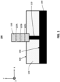
- FIG. 1 illustrates an electrical contact structure 110 that couples a semiconductor structure 120 to a backside metal layer 130, according to some embodiments of the disclosure.
- FIG. 1 also shows a substrate 140 in which the electrical contact structure 110 is arranged.
- the substrate 140 includes two surfaces 150 and 160.
- the surface 150 opposes the surface 160.
- the side of the substrate 140 from the surface 150 downwards is referred to as the backside of the substrate 140, and the side of the substrate 140 from the surface 160 upwards is referred to as the frontside.
- the surface 150 is the referred to as backside surface
- the surface 160 is referred to as the frontside surface.
- Various layers can be arranged in the frontside and backside of the substrate 140.
- the backside metal layer 130 is arrange at the backside of the substrate 140. Even though not shown in FIG. 1 , one or more metal layers may be arranged at the frontside of the substrate 140.
- the electrical contact structure 110 is inside the substrate 140 and is between the surfaces 150 and 160.
- the electrical contact structure 110 is an electrically conductive structure that provides an electrical connection between the semiconductor structure 120 and the backside metal layer 130.
- An end of the electrical contact structure 110 is connected to the semiconductor structure 120, and the opposing end of the electrical contact structure 110 is connected to the backside metal layer 130.
- the substrate 140 encloses the whole electrical contact structure 110. In other embodiments, the substrate 140 may enclose a portion of the electrical contact structure 110.
- the semiconductor structure 120 is partially inside the substrate 140. A portion of the semiconductor structure 120 is outside the substrate 140 and is at the frontside of the substrate 140.
- the semiconductor structure 120 may be an epitaxial semiconductor structure that includes a crystalline structure of a semiconductor material.
- the semiconductor structure 120 may be formed using an epitaxy process. For instance, a recess may be formed at the surface 160 of the substrate 140. An epitaxial deposition process may then be carried out to fill the recesses with one or more materials used to fabricate the semiconductor structure 120.
- the semiconductor structure 120 may be formed around three elongated semiconductor structures 125A-125C (collectively referred to as "elongated semiconductor structures 125" or “elongated semiconductor structure 125"). Each elongated semiconductor structure 125 may be partially or wholly enclosed by the semiconductor structure 120. Even though FIG. 1 shows three elongated semiconductor structures 125, there can be a different number of elongated semiconductor structures 125 associated with the semiconductor structure 120.
- An elongated semiconductor structure 125 may be a non-planar structure, i.e., a three-dimensional structure, such as fin, nanoribbon, or nanowire.
- An elongated semiconductor structure 125 may have a longitudinal axis and a transvers cross-section perpendicular to the longitudinal axis.
- a dimension of the elongated semiconductor structure 125 along the longitudinal axis may be greater than dimensions along other directions, e.g., directions along axes perpendicular to the longitudinal axis.
- the elongated semiconductor structures 125 are nanoribbons having longitudinal axes along the X axis and transvers cross-sections in the Y-Z plane.
- the longitudinal axes of the elongated semiconductor structures 125 can be in parallel. With the orientation of the semiconductor structure 120 shown in FIG. 1 , the elongated semiconductor structures 125 extends horizontally (i.e., along the X axis in FIG. 1 ) but stacked vertically (i.e., along the Y axis).
- the semiconductor structure 120 and the elongated semiconductor structures 125 may include a same semiconductor material or different semiconductor materials.
- the semiconductor material in the semiconductor structure 120 may be a Group IV material, a compound of Group IV materials, a Group III/V material, a compound of Group III/V materials, a Group II/VI material, a compound of Group II/VI materials, or other semiconductor materials.
- Example Group II materials include zinc (Zn), cadmium (Cd), and so on.
- Example Group III materials include aluminum (Al), boron (B), indium (In), gallium (Ga), and so on.
- Example Group IV materials include silicon (Si), germanium (Ge), carbon (C), etc.
- Example Group V materials include nitrogen (N), phosphorus (P), arsenic (As), antimony (Sb), and so on.
- Example Group VI materials include sulfur (S), selenium (Se), tellurium (Te), oxygen (O), and so on.
- a compound of Group IV materials can be a binary compound, such as SiC, SiGe, and so on.
- a compound of Group III/V materials can be a binary, tertiary, or quaternary compound, such as GaN, InN, and so on.
- a compound of Group II/VI materials can be a binary, tertiary, or quaternary compounds, such as CdSe, CdS, CdTe, ZnO, ZnSe, ZnS, ZnTe, CdZnTe, CZT, HgCdTe, HgZnTe, and so on.
- the semiconductor structure 120 is doped.
- the dopants in the semiconductor structure 120 may be n-type dopants or p-type dopants.
- Example n-type dopants include Te, S, As, tin (Sn), Si, Ga, Se, S, In, Al, Cd, chlorine (CI), iodine (I), fluorine (F), and so on.
- Example p-type dopants include beryllium (Be), Zn, magnesium (Mg), Sn, P, Te, lithium (Li), sodium (Na), Ga, Cd, and so on.
- the semiconductor structure 120 may be highly doped, e.g., with a dopant concentration of about 1 ⁇ 10 20 to 1 ⁇ 10 21 dopants per cubic centimeter (cm -3 ) in order to form a terminal of a varactor device.
- the dopant concentration in the semiconductor structure 120 may be the dopant concentration of a semiconductor material in the semiconductor structure 120.
- the dopant concentration is a concentration of n-type dopants.
- the semiconductor structure 120 may be the regions having dopant concentrations higher than in other regions, e.g., higher than a dopant concentration in an elongated semiconductor structure 125 and, therefore, may be referred to as highly doped regions.
- a dopant concentration in the semiconductor structure 120 is 10 to 1000 times higher than a dopant concentration in an elongated semiconductor structure 125.
- the semiconductor material of an elongated semiconductor structure 125 may be an intrinsic (e.g., undoped) semiconductor material or alloy, not intentionally doped with any electrically active impurity.
- nominal impurity dopant levels may be present in the elongated semiconductor structure 125.
- impurity dopant level within the elongated semiconductor structure 125 can be significantly lower than the dopant level in the semiconductor structure 120.
- the dopant concentration in the elongated semiconductor structure 125 may be in a range from 1 ⁇ 10 18 to 1 ⁇ 10 19 cm -3 , which may be 10 to 1000 times lower than the dopant concentration in the semiconductor structure 120
- the substrate 140 may be any suitable structure based on which the semiconductor structure 120 can be built, e.g., a die, a wafer, or a chip. Therefore, the substrate 140 may be referred to as a "support structure.”
- the substrate 140 may be a printed circuit board (PCB) substrate.
- the substrate 140 is a semiconductor substrate, which is composed of semiconductor material systems including, for example, n-type or p-type materials systems.
- the semiconductor substrate may be a crystalline substrate formed using a bulk silicon or a silicon-on-insulator substructure.
- the semiconductor substrate may be formed using alternate materials, which may or may not be combined with silicon, that include but are not limited to germanium, indium antimonide, lead telluride, indium arsenide, indium phosphide, gallium arsenide, indium gallium arsenide, gallium antimonide, or other combinations of Group III-V, Group II-VI, or Group IV materials.
- the substrate may be non-crystalline.
- the substrate 140 may include any such substrate material that provides a suitable surface for forming the fill pattern.
- the substrate may, e.g., be the wafer 2000 of FIG. 11A , discussed below, and may be, or be included in, a die, e.g., the singulated die 2002 of FIG. 11B , discussed below.
- the semiconductor structure 120 functions as a terminal of a varactor device.
- the backside metal layer 130 may be a ground plane.
- the semiconductor structure 120 can be grounded.
- a dimension of the substrate 140 along the Y axis i.e., a distance from the surface 150 to the surface 160
- the dimension of the electrical contact structure 110 along the Y axis can be less than 50-70 nanometers.
- the electrical contact structure 110 provides an electrical connection route with a minimized distance between the semiconductor structure 120 and the backside metal layer 130.With the electrical connection route facilitated by the electrical contact structure 110, the varactor device can have better performance than conventional varactor devices, such as the one shown in FIG. 2 .
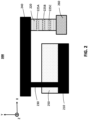
- FIG. 2 is a cross-sectional view of a varactor device 200 without backside electrical contact, according to some embodiments of the disclosure.
- the varactor device 200 includes a backside metal layer 210, a semiconductor structure 220, elongated semiconductor structures 225A-225C, a feedthrough via 230, a trench contact 240, a substrate 250, and an electrical insulator 260.
- the varactor device 200 may include fewer, more, or different components.
- the backside metal layer 210 may be the same or similar as the backside metal layer 130.
- the semiconductor structure 220 may be the same or similar as the semiconductor structure 120.
- the semiconductor structure 220 is a terminal of the varactor device 200.
- the elongated semiconductor structures 225A-225C may be the same or similar as the elongated semiconductor structures 125.
- the substrate 250 may be the same or similar as the substrate 140.
- the semiconductor structure 220 is coupled to the backside metal layer 210 through an electrical connection route that includes the feedthrough via 230 and the trench contact 240.
- the electrical connection route in FIG. 2 can still be significantly longer than the electrical connection route in FIG. 1 .
- the parasitic resistance of the varactor device 200 would be higher, which undermines the Q factor of the varactor device 200.
- the trench contact 240 may form additional capacitance, e.g., with another terminal of the varactor device 200.
- varactor devices with the electrical contact structure 110 in FIG. 1 can have better Q factor and better capacitance ratio, i.e., better performance.
- FIG. 3 is a cross-sectional view of a two-terminal varactor device 300 with backside electrical contact, according to some embodiments of the disclosure.
- the varactor device 300 includes a contact structure 310, a semiconductor structure 320, elongated semiconductor structures 325A-325C (collectively referred to as "elongated semiconductor structures 325" or "elongated semiconductor structure 325"), an electrically conductive layer 330, a substrate 340, a gate 370, and another electrically conductive layer 380.
- the electrically conductive layers 330 and 380 constitute the two terminals of the varactor device 300 and can provide two different signals.
- the varactor device 300 may include fewer, more, or different components.
- the contact structure 310 includes an electrically conductive material, such as metal.
- the contact structure 310 is inside the substrate 340.
- the substrate 340 includes two surfaces 350 and 360.
- the surface 350 opposes the surface 360.
- the side of the substrate 340 from the surface 350 downwards is referred to as the backside of the substrate 340, and the side of the substrate 340 from the surface 360 upwards is referred to as the frontside.
- the surface 350 is the referred to as backside surface
- the surface 360 is referred to as the frontside surface.
- Various layers can be arranged in the frontside and backside of the substrate 340.
- the electrically conductive layer 330 is arrange at the backside of the substrate 340, and the electrically conductive layer 380 arranged at the frontside of the substrate 340.
- the substrate 340 may be an embodiment of the substrate 140 in FIG. 1 .
- the semiconductor structure 320 includes a doped semiconductor material, such as one of the semiconductor materials described above.
- the semiconductor structure 320 may be doped with n-type dopants.
- a concentration of dopants in the semiconductor structure 320 can be in a range from 1 ⁇ 10 20 to 1 ⁇ 10 21 cm -3 .
- the semiconductor structure 320 may be an epitaxial structure that includes a crystalline structure of the semiconductor material.
- the semiconductor structure 320 may be an embodiment of the semiconductor structure 120 in FIG. 1 .
- an end of the semiconductor structure 320 i.e., the end in the substrate 340 in FIG. 3
- an end of the contact structure 310 i.e., the end that is closer to the surface 360 than the surface 350.
- the other end of the contact structure 310 is at the surface 350 and is connected to the electrically conductive layer 330.
- the electrically conductive layer 330 is a ground plane, and the semiconductor structure 320 can be grounded.
- the semiconductor structure 320 is connected to the elongated semiconductor structures 325.
- the semiconductor structure 320 is formed around a portion of each of the elongated semiconductor structures 325, such as a portion that is enclosed by the semiconductor structure 320.
- the portion of the elongated semiconductor structure 325 may be highly doped.
- the concentration of dopants in the portion of the elongated semiconductor structure 325 may be the same or similar as the concentration of dopants in the semiconductor structure 320.
- the portion of the elongated semiconductor structure 325 may be doped with the same type of dopants as the semiconductor structure 320.
- the semiconductor structure 320 is formed adjacent to the elongated semiconductor structures 325.
- the elongated semiconductor structures 325 are non-planar semiconductor structures, such as nanoribbons.
- the elongated semiconductor structures 325 can be arranged in parallel. For instance, longitudinal axes of the elongated semiconductor structures 325 can be in parallel, e.g., along the X axis. At least a portion of each elongated semiconductor structures 325, such as the portion wrapped around by the gate 370, may be undoped or lowly doped. In some embodiments, A concentration of dopants in the elongated semiconductor structures 325 can be in a range from 1 ⁇ 10 18 to 1 ⁇ 10 19 cm -3 .
- Some or all of the elongated semiconductor structures 325 can either be inverted or accumulated, depending on the doping type in the elongated semiconductor structures 525.
- An elongated semiconductor structure 325 may be an embodiment of an elongated semiconductor structure 125 in FIG. 1 .
- the elongated semiconductor structures 325 are coupled to a gate 370.
- the gate is around a portion of each of the elongated semiconductor structures 325.
- the gate 370 is coupled to the electrically conductive layer 380.
- the electrically conductive layer 380 may be a power plane or signal power that can provide electrical power or signal to the gate 370.
- a region 390 between the semiconductor structure 320 and the gate 370 can be an electrically insulating region, e.g., a depletion region.
- the semiconductor structure 320, the gate 370, and the region 390 can constitute a variable capacitor.
- the region 390 may include a portion of each of the elongated semiconductor structures 325.
- the region 390 may include an electrical insulator surrounding the portions of the elongated semiconductor structures 325.
- a portion 345 of the substrate 340 which is under the gate 370, may be doped with an opposing type of dopants from the semiconductor structure 320. As the portion 345 of the substrate 340 and the semiconductor structure 320 is counter doped, parasitic conduction path through the substrate 340 can be avoided. Additionally or alternatively, one or more of the elongated semiconductor structures 325 are doped, e.g., with the same type of dopants as the semiconductor structure 320.
- the varactor device 300 may operate either as an accumulation mode device or as an inversion mode device.
- FIG. 4 is another cross-sectional view of the two-terminal varactor device 300 in FIG. 3 , according to some embodiments of the disclosure.
- FIG. 4 shows a cross-section 400 of the varactor device 300 in the A-B plane shown in FIG. 3 .
- the gate 370 includes gate insulators 377A-377C and 379 and a gate electrode 375.
- a gate insulator includes an electrical insulator, such as a dielectric material, hysteretic material, and so on.
- Example dielectric material includes oxide (e.g., Si based oxides, metal oxides, etc.), high-k dielectric, and so on.
- Example hysteretic material include ferroelectric materials, antiferroelectric materials, etc.
- Each of the gate insulators 377A-377C encloses a different elongated semiconductor structure 325 to insulate the elongated semiconductor structure 325 from the gate electrode 375.
- the gate insulator 379 surrounds a portion of the substrate 340 to insulate the substrate 340 from the gate electrode 375.
- the gate insulator 379 is closer to the surface 360 than the surface 350 of the substrate 340.
- the gate electrode 375 includes an electrically conductive material, e.g., metal.
- the gate electrode 375 is coupled to the electrically conductive layer 380.
- FIG. 5 is a cross-sectional view of another two-terminal varactor device 500 with backside electrical contact, according to some embodiments of the disclosure.
- the varactor device 500 includes five contact structures 510A-510E (collectively referred to as “contact structures 510" or “contact structure 510"), five semiconductor structures 520A-520E (collectively referred to as “semiconductor structures 520" or “semiconductor structure 520”), three elongated semiconductor structures 525A-325C (collectively referred to as “elongated semiconductor structures 525" or "elongated semiconductor structure 525"), an electrically conductive layer 530, a substrate 540, four gates 570A-570D (collectively referred to as “gates 570" or “gate 570”), and another electrically conductive layer 580.
- the electrically conductive layers 530 and 580 constitute the two terminals of the varactor device 500.
- the varactor device 500 may include fewer, more, or different components, such as a different number of contact structure, semiconductor structures, elongated semiconductor structures, gates, or electrically conductive layers.
- Each contact structure 510 includes an electrically conductive material, such as metal.
- Each contact structure 510 is inside the substrate 540 and extends between two surfaces 550 and 560 of the substrate 540.
- the surface 550 opposes the surface 560.
- the side of the substrate 540 from the surface 550 downwards is referred to as the backside of the substrate 540, and the side of the substrate 540 from the surface 560 upwards is referred to as the frontside.
- the surface 550 is the referred to as backside surface, the surface 560 is referred to as the frontside surface.
- Various layers can be arranged in the frontside and backside of the substrate 540.
- the electrically conductive layer 530 is arrange at the backside of the substrate 540, and the electrically conductive layer 580 arranged at the frontside of the substrate 540.
- the substrate 540 may be an embodiment of the substrate 140 in FIG. 1 .
- Each contact structure 510 is paired with a different semiconductor structure 520 and couples the semiconductor structure 520 to the electrically conductive layer 530.
- Each semiconductor structure 520 includes a doped semiconductor material, such as one of the semiconductor materials described above. A concentration of dopants in the semiconductor structure 520 can be in a range from 1 ⁇ 10 20 to 1 ⁇ 10 21 cm -3 .
- the semiconductor structure 520 may be an epitaxial structure that includes a crystalline structure of the semiconductor material.
- the semiconductor structure 520 may be an embodiment of the semiconductor structure 120 in FIG. 1 . As shown in FIG. 5 , an end of a semiconductor structure 520 (i.e., the end in the substrate 540 in FIG.
- the electrically conductive layer 530 is a ground plane, and the semiconductor structure 520 can be grounded.
- an elongated semiconductor structure 525 is a continuous structure that extends between the semiconductor structure 520A and the semiconductor structure 520E.
- an elongated semiconductor structure 525 may include a plurality of discrete portions, each of which is between two adjacent semiconductor structures 520, such as a first portion between the semiconductor structure 520A and the semiconductor structure 520B, a second portion between the semiconductor structure 520B and the semiconductor structure 520C, a third portion between the semiconductor structure 520C and the semiconductor structure 520D, and a fourth portion between the semiconductor structure 520D and the semiconductor structure 520E.
- the semiconductor structure 520 is formed around a portion of each of the elongated semiconductor structures 525, such as a portion that is enclosed by the semiconductor structure 520. In alternative embodiments, the semiconductor structure 520 is formed adjacent to the elongated semiconductor structures 525.
- the elongated semiconductor structures 525 are non-planar semiconductor structures, such as nanoribbons.
- the elongated semiconductor structures 525 may be undoped or lowly doped.
- a concentration of dopants in the elongated semiconductor structures 525 can be in a range from 1 ⁇ 10 18 to 1 ⁇ 10 19 cm -3 .
- An elongated semiconductor structure 525 may be an embodiment of an elongated semiconductor structure 125 in FIG. 1 .
- the elongated semiconductor structures 525 are coupled to the four gates 570.
- Each gate 570 is around a portion of each of the elongated semiconductor structures 525.
- the gates 570 are coupled to the electrically conductive layer 580.
- the electrically conductive layer 580 may be a power plane or signal power that can provide electrical power or signal to the gate 570.
- the semiconductor structures 520 are grounded and the gates 570 are polarized, there can be an electrical potential between a semiconductor structure 520 and the gate 570 that is adjacent to the semiconductor structure 520.
- the region between the semiconductor structure 520 and the corresponding gate 570 can be an electrically insulating region, e.g., a depletion region.
- an elongated semiconductor structure 525 (or all the elongated semiconductor structures 525) can be encapsulated by an electrical insulator of the gate 570.
- the elongated semiconductor structure 525 can either be inverted or accumulated, depending on the doping type in the elongated semiconductor structure 525.
- the semiconductor structure 520, the gate 570, and the region can constitute a variable capacitor.
- the varactor device 500 includes a series of variable capacitors.
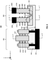
- FIG. 6 is a cross-sectional view of a three-terminal varactor device 600 with backside electrical contact, according to some embodiments of the disclosure.
- the varactor device 600 includes two sections 601 and 602 that share a substrate 640, which may be an embodiment of the substrate 140 in FIG. 1 .
- the section 601 includes contact structures 610A and 610B (collectively referred to as “contact structures 610” or “contact structure 610"), semiconductor structures 620A and 620B (collectively referred to as “semiconductor structures 620” or “semiconductor structure 620”), elongated semiconductor structures 625A-625C (collectively referred to as “elongated semiconductor structures 625" or “elongated semiconductor structure 625"), an electrically conductive layer 630, a gates 670, and another electrically conductive layer 675.
- the section 602 includes elongated semiconductor structures 635A-635C (collectively referred to as “elongated semiconductor structures 635" or “elongated semiconductor structure 635"), elongated semiconductor structures 645A-645C (collectively referred to as “elongated semiconductor structures 645" or “elongated semiconductor structure 645"), gates 680A and 680B, and electrically conductive layers 680A and 680B.
- the varactor device 600 may include fewer, more, or different components.
- the electrically conductive layers 630, 680A, and 680B constitute the three terminals of the varactor device 600.
- the electrically conductive layer 630 is a ground plane
- the electrically conductive layers 680A and 680B are signal planes that can provide signals of opposite polarity.
- the substrate 640 includes surfaces 650 and 660.
- the surface 650 opposes the surface 660.
- the side of the substrate 640 from the surface 650 downwards is referred to as the backside of the substrate 640, and the side of the substrate 640 from the surface 660 upwards is referred to as the frontside.
- the surface 650 is the referred to as backside surface
- the surface 660 is referred to as the frontside surface.
- Various layers can be arranged in the frontside and backside of the substrate 640.
- the electrically conductive layer 630 is arrange at the backside of the substrate 640
- the electrically conductive layers 680A and 680B are arranged at the frontside of the substrate 640.
- the substrate 640 may be an embodiment of the substrate 140 in FIG. 1 .
- the section 601 may be a tap structure of the varactor device 600.
- the section 601 may be used as a virtual ground biased at a DC voltage for determining the differential capacitance between the two gates 675A and 675B.
- the electrically conductive layer 630 is at the backside of the substrate 640.
- the contact structure 610A couples the semiconductor structure 620A to the electrically conductive layer 630.
- the contact structure 610B couples the semiconductor structure 620B to the electrically conductive layer 630.
- Each of the elongated semiconductor structures 625 extend from the semiconductor structure 620A to the semiconductor structure 620B. A portion of each elongated semiconductor structure 625 is wrapped around by the gate 670.
- the elongated semiconductor structures 625 can be arranged in parallel. For instance, longitudinal axes of the elongated semiconductor structures 625 can be in parallel, e.g., along the X axis.
- Each contact structure 610 may be an embodiment of the electrical contact structure 110 in FIG. 1 or the contact structure 310 in FIG. 3 .
- Each semiconductor structure 620 may be an embodiment of the semiconductor structure 120 in FIG. 1 or the semiconductor structure 320 in FIG. 3 .
- Each elongated semiconductor structure 625 may be an embodiment of the elongated semiconductor structure 125 in FIG. 1 or the elongated semiconductor structure 325 in FIG. 3 .
- the electrically conductive layer 630 may be an embodiment of the backside metal layer 130 in FIG. 1 or the electrically conductive layer 330 in FIG. 3 .
- the gate 670 may be an embodiment of the gate 370 in FIG. 3 .
- the gates 675A and 675B can be polarized.
- the gates 675A and 675B have differential polarity.
- the gates 675A and 675B may have the same type of polarity (e.g., positive or negative polarity), but the gate 675A is set to a high polarity and the gate 675B is set to low polarity, or the gate 675B is set to high polarity and the gate 675A is set to low polarity.
- the gates 675A and 675B may have different types of polarity, e.g., the gate 675A is set to positive polarity and the gate 675B is set to negative polarity, or the gate 675B is set to positive polarity and the gate 675A is set to negative polarity.
- the gate 675A is coupled to the elongated semiconductor structures 635 and wraps around a portion of each elongated semiconductor structure 635.
- the gate 675B is coupled to the elongated semiconductor structures 645 and wraps around a portion of each elongated semiconductor structure 645.
- the elongated semiconductor structures 635 and 645 may be undoped or lowly doped. In some embodiments, the elongated semiconductor structures 635 and 645 may function as channel regions coupled to the gates 675A and 675B, respectively.
- the gate 675A is coupled to the electrically conductive layer 680A, and the gate 675A is coupled to the electrically conductive layer 680B.
- the electrically conductive layers 680A and 680B may be two power planes or signals planes and can provide different electrical signals.
- the electrically conductive layers 680A and 680B may be separated by one or more electrical insulators.
- the gates 675A and 675B may be separated by one or more electrical insulators.
- Electrical charges can be transferred between the gate 675A and the gate 675B, or the other way around, through a charge conduction path 665 in a portion 690 of the substrate 640.
- the charge conduction path 665 is from the gate 675A to the gate 675B.
- the charge conduction path 665 is from the gate 675B to the gate 675A.
- the portion 690 is over (e.g., underneath) the gates 675A and 675B.
- the portion 690 may be doped to reduce resistance and increase the Q factor of the varactor device 600.
- a concentration of dopants in the portion 690 is higher than a concentration of dopants in the rest of the substrate 640, such as two to three times higher.
- the concentration of dopants in the portion 690 may be in a range from 1 ⁇ 10 18 to 1 ⁇ 10 18 cm -3 .
- An opening 695 between the two gates 675A and 675B is formed in the portion 690.
- the opening 695 is at the surface 660.
- the gate 675A has a width W 1 along the Z axis.
- the gate 675B may also have the width W 1 .
- the opening 695 has a width W 2 along the Z axis.
- the width W 1 may be in a range from 12-20 nanometers
- the width W 2 may be in a range from 30-50 nanometers. The greater the width W 1 , the large charge accumulation on the gate 675A, the larger the maximum capacitance of the varactor device 600, and the larger the capacitance ratio of the varactor device 600.
- the gates 675A and 675B or the opening 695 may be formed by EUV patterning to form wider gates and narrower opening to achieve optimal performance of the varactor device 600.
- FIG. 7 is another cross-sectional view of the three-terminal varactor device in FIG. 6 , according to some embodiments of the disclosure.
- FIG. 7 shows a cross-section 700 of the varactor device 600 in the A-B plane shown in FIG. 6 .
- the gate 670 includes gate insulators 677A-677C and 679 and a gate electrode 673.
- Each of the gate insulators 677A-377C encloses a different elongated semiconductor structure 625 to insulate the elongated semiconductor structure 625 from the gate electrode 673.
- the gate insulator 679 surrounds a portion of the substrate 640 to insulate the substrate 640 from the gate electrode 673.
- the gate insulator 679 is closer to the surface 660 than the surface 650 of the substrate 640.
- the gate electrode 673 includes an electrically conductive material, e.g., metal.
- FIG. 8 is yet another cross-sectional view of the three-terminal varactor device in FIG. 6 , according to some embodiments of the disclosure.
- FIG. 8 shows a cross-section 800 of the varactor device 600 in the C-D plane shown in FIG. 6 .
- the gate 675A includes a gate electrode 672 and gate insulators 674A-674C and 676.
- Each of the gate insulators 674A-674C encloses a different elongated semiconductor structure 635 to insulate the elongated semiconductor structure 635 from the gate electrode 672.
- the gate insulator 676 surrounds a part of the portion 690 of the substrate 640 to insulate the portion 690 of the substrate 640 from the gate electrode 672.
- the charge conduction path 665 comes out from the C-D plane, which is shown as the circle dot in FIG. 8 .
- FIG. 9 is yet another cross-sectional view of the three-terminal varactor device in FIG. 6 , according to some embodiments of the disclosure.
- FIG. 9 shows a cross-section 900 of the varactor device 600 in the E-F plane shown in FIG. 6 .
- the gate 675B includes a gate electrode 682 and gate insulators 684A-684C and 686.
- Each of the gate insulators 684A-684C encloses a different elongated semiconductor structure 645 to insulate the elongated semiconductor structure 645 from the gate electrode 682.
- the gate insulator 686 surrounds a part of the portion 690 of the substrate 640 to insulate the portion 690 of the substrate 640 from the gate electrode 682.
- the charge conduction path 665 comes into the E-F plane, which is shown as the circled cross in FIG. 9 .
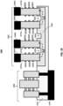
- FIG. 10 is a cross-sectional view of another three-terminal varactor device 1000 with backside electrical contact, according to some embodiments of the disclosure.
- the three terminals of the varactor device 1000 are electrically conductive layers 1030, 1080A, and 1080B.
- the electrically conductive layer 1030 is arranged at the frontside of a substrate 1040, versus the electrically conductive layers 1080A and 1080B are arranged at the backside of the substrate 1040.
- the electrically conductive layers 1080A and 1080B are not continuous.
- Each of the electrically conductive layers 1080A and 1080B includes discrete sections that may receive the same signal and have the same polarity.
- the polarity of the electrically conductive layers 1080A may be opposite to the polarity of the electrically conductive layers 1080B.
- the varactor device 1000 includes two sections 1001 and 1002.
- the section 1001 may be a tap structure of the varactor device 1000.
- the section 1001 is the same or similar as the section 601 in FIG. 6 .
- the section 1002 in FIG. 10 includes two pairs of oppositely polarized gates: four gates 1070A, 1070B, 1075A, and 1075B.
- the section 1002 may include more pairs of oppositely polarized gates.
- the gates 1070A and 1075A are coupled to different sections of the electrically conductive layer 1080A.
- the gates 1070B and 1075B are coupled to different sections of the electrically conductive layer 1080B.
- the gate 1070A may have an opposite polarity from the gate 1070B
- the gate 1075A may have an opposite polarity from the gate 1075B.
- a charge conduction path 1060 from the gate 1070A to the gate 1070B and another charge conduction path 1065 from the gate 1075A to the gate 1075B are present in a portion 1090 of the substrate 1040.
- the portion 1090 may be highly doped, e.g., with the same type of dopants as semiconductor structures in the section 1001.
- the charge conduction paths 1060 is from the gate 1070A to the gate 1070B. Adjacent gates of the four gates 1070A, 1070B, 1075A, and 1075B are separated from each other through openings 1095A-1095C formed in the portion 1090.
- the opening 1095A is between the gate 1080A and the gate 1080B, particularly between the portion of the gate 1080A in the portion 1090 and the portion of the gate 1080A in the portion 1090.
- the gates 1070A, 1070B, 1075A, and 1075B or the opening 1095A-1095C may be formed by EUV patterning to form wider gates or narrower opening to achieve optimal performance of the varactor device 1000.
- FIGS. 11A-11B are top views of a wafer 2000 and dies 2002 that may include one or more varactor devices with backside electrical contact, according to some embodiments of the disclosure.
- the dies 2002 may be included in an IC package, according to some embodiments of the disclosure.
- any of the dies 2002 may serve as any of the dies 2256 in an IC package 2200 shown in FIG. 12 .
- the wafer 2000 may be composed of semiconductor material and may include one or more dies 2002 having IC devices formed on a surface of the wafer 2000.
- Each of the dies 2002 may be a repeating unit of a semiconductor product that includes any suitable IC (e.g., ICs including one or more varactor devices as described herein).
- the wafer 2000 may undergo a singulation process in which each of the dies 2002 is separated from one another to provide discrete "chips" of the semiconductor product.
- devices that include one or more varactor devices as disclosed herein may take the form of the wafer 2000 (e.g., not singulated) or the form of the die 2002 (e.g., singulated).
- the die 2002 may include one or more diodes (e.g., one or more varactor devices as described herein), one or more transistors (e.g., one or more III-N transistors as described herein) as well as, optionally, supporting circuitry to route electrical signals to the III-N diodes with n-doped wells and capping layers and III-N transistors, as well as any other IC components.
- the wafer 2000 or the die 2002 may implement an electrostatic discharge (ESD) protection device, an RF FE device, a memory device (e.g., a static random-access memory (SRAM) device), a logic device (e.g., an AND, OR, NAND, or NOR gate), or any other suitable circuit element. Multiple ones of these devices may be combined on a single die 2002.
- FIG. 12 is a side, cross-sectional view of an example IC package 2200 that may include one or more IC devices having varactor devices with backside electrical contact, according to some embodiments of the disclosure.
- the IC package 2200 may be a system-in-package (SiP).
- the IC package 2200 may include a package substrate 2252.
- the package substrate 2252 may be formed of a dielectric material (e.g., a ceramic, a glass, a combination of organic and inorganic materials, a buildup film, an epoxy film having filler particles therein, etc., and may have embedded portions having different materials), and may have conductive pathways extending through the dielectric material between the face 2272 and the face 2274, or between different locations on the face 2272, and/or between different locations on the face 2274.
- a dielectric material e.g., a ceramic, a glass, a combination of organic and inorganic materials, a buildup film, an epoxy film having filler particles therein, etc.
- the package substrate 2252 may include conductive contacts 2263 that are coupled to conductive pathways 2262 through the package substrate 2252, allowing circuitry within the dies 2256 and/or the interposer 2257 to electrically couple to various ones of the conductive contacts 2264 (or to other devices included in the package substrate 2252, not shown).
- the IC package 2200 may include an interposer 2257 coupled to the package substrate 2252 via conductive contacts 2261 of the interposer 2257, first-level interconnects 2265, and the conductive contacts 2263 of the package substrate 2252.
- the first-level interconnects 2265 illustrated in FIG. 12 are solder bumps, but any suitable first-level interconnects 2265 may be used.
- no interposer 2257 may be included in the IC package 2200; instead, the dies 2256 may be coupled directly to the conductive contacts 2263 at the face 2272 by first-level interconnects 2265.
- the IC package 2200 may include one or more dies 2256 coupled to the interposer 2257 via conductive contacts 2254 of the dies 2256, first-level interconnects 2258, and conductive contacts 2260 of the interposer 2257.
- the conductive contacts 2260 may be coupled to conductive pathways (not shown) through the interposer 2257, allowing circuitry within the dies 2256 to electrically couple to various ones of the conductive contacts 2261 (or to other devices included in the interposer 2257, not shown).
- the first-level interconnects 2258 illustrated in FIG. 12 are solder bumps, but any suitable first-level interconnects 2258 may be used.
- a "conductive contact” may refer to a portion of electrically conductive material (e.g., metal) serving as an interface between different components; conductive contacts may be recessed in, flush with, or extending away from a surface of a component, and may take any suitable form (e.g., a conductive pad or socket).
- electrically conductive material e.g., metal
- an underfill material 2266 may be disposed between the package substrate 2252 and the interposer 2257 around the first-level interconnects 2265, and a mold compound 2268 may be disposed around the dies 2256 and the interposer 2257 and in contact with the package substrate 2252.
- the underfill material 2266 may be the same as the mold compound 2268.
- Example materials that may be used for the underfill material 2266 and the mold compound 2268 are epoxy mold materials, as suitable.
- Second-level interconnects 2270 may be coupled to the conductive contacts 2264. The second-level interconnects 2270 illustrated in FIG.
- solder balls e.g., for a ball grid array arrangement
- any suitable second-level interconnects 22770 may be used (e.g., pins in a pin grid array arrangement or lands in a land grid array arrangement).
- the second-level interconnects 2270 may be used to couple the IC package 2200 to another component, such as a circuit board (e.g., a motherboard), an interposer, or another IC package, as known in the art and as discussed below with reference to FIG. 13 .
- the dies 2256 may take the form of any of the embodiments of the die 2002 discussed herein and may include any of the embodiments of an IC device having one or more varactor devices. In embodiments in which the IC package 2200 includes multiple dies 2256, the IC package 2200 may be referred to as a multi-chip package. Importantly, even in such embodiments of an MCP implementation of the IC package 2200, one or more varactor devices may be provided in a single chip, in accordance with any of the embodiments described herein.
- the dies 2256 may include circuitry to perform any desired functionality.
- one or more of the dies 2256 may be ESD protection dies, including one or more varactor devices as described herein, one or more of the dies 2256 may be logic dies (e.g., silicon-based dies), one or more of the dies 2256 may be memory dies (e.g., high bandwidth memory), etc. In some embodiments, any of the dies 2256 may include one or more varactor devices, e.g., as discussed above; in some embodiments, at least some of the dies 2256 may not include any III-N diodes with n-doped wells and capping layers.
- the IC package 2200 illustrated in FIG. 12 may be a flip chip package, although other package architectures may be used.
- the IC package 2200 may be a ball grid array (BGA) package, such as an embedded wafer-level ball grid array (eWLB) package.
- the IC package 2200 may be a wafer-level chip scale package (WLCSP) or a panel fan-out (FO) package.
- BGA ball grid array
- eWLB embedded wafer-level ball grid array
- WLCSP wafer-level chip scale package
- FO panel fan-out
- An IC package 2200 may include additional passive components, such as surface-mount resistors, capacitors, and inductors disposed on the first face 2272 or the second face 2274 of the package substrate 2252, or on either face of the interposer 2257. More generally, an IC package 2200 may include any other active or passive components known in the art.
- FIG. 13 is a cross-sectional side view of an IC device assembly 2300 that may include components having one or more IC devices implementing varactor devices with backside electrical contact, according to some embodiments of the disclosure.
- the IC device assembly 2300 includes a number of components disposed on a circuit board 2302 (which may be, e.g., a motherboard).
- the IC device assembly 2300 includes components disposed on a first face 2340 of the circuit board 2302 and an opposing second face 2342 of the circuit board 2302; generally, components may be disposed on one or both faces 2340 and 2342.
- any suitable ones of the components of the IC device assembly 2300 may include any of the IC devices implementing one or more varactor devices in accordance with any of the embodiments disclosed herein; e.g., any of the IC packages discussed below with reference to the IC device assembly 2300 may take the form of any of the embodiments of the IC package 2200 discussed above with reference to FIG. 12 (e.g., may include one or more varactor devices in/on a die 2256).
- the circuit board 2302 may be a PCB including multiple metal layers separated from one another by layers of dielectric material and interconnected by electrically conductive vias. Any one or more of the metal layers may be formed in a desired circuit pattern to route electrical signals (optionally in conjunction with other metal layers) between the components coupled to the circuit board 2302. In other embodiments, the circuit board 2302 may be a non-PCB substrate.
- the IC device assembly 2300 illustrated in FIG. 13 includes a package-on-interposer structure 2336 coupled to the first face 2340 of the circuit board 2302 by coupling components 2316.
- the coupling components 2316 may electrically and mechanically couple the package-on-interposer structure 2336 to the circuit board 2302, and may include solder balls (e.g., as shown in FIG. 13 ), male and female portions of a socket, an adhesive, an underfill material, and/or any other suitable electrical and/or mechanical coupling structure.
- the package-on-interposer structure 2336 may include an IC package 2320 coupled to an interposer 2304 by coupling components 2318.
- the coupling components 2318 may take any suitable form for the application, such as the forms discussed above with reference to the coupling components 2316.
- the IC package 2320 may be or include, for example, a die (the die 2002 of FIG. 11B ), an IC device (e.g., the IC device of FIGS. 1-2 ), or any other suitable component.
- the IC package 2320 may include one or more varactor devices as described herein. Although a single IC package 2320 is shown in FIG. 13 , multiple IC packages may be coupled to the interposer 2304; indeed, additional interposers may be coupled to the interposer 2304.
- the interposer 2304 may provide an intervening substrate used to bridge the circuit board 2302 and the IC package 2320. Generally, the interposer 2304 may spread a connection to a wider pitch or reroute a connection to a different connection. For example, the interposer 2304 may couple the IC package 2320 (e.g., a die) to a BGA of the coupling components 2316 for coupling to the circuit board 2302. In the embodiment illustrated in FIG. 13 , the IC package 2320 and the circuit board 2302 are attached to opposing sides of the interposer 2304; in other embodiments, the IC package 2320 and the circuit board 2302 may be attached to a same side of the interposer 2304. In some embodiments, three or more components may be interconnected by way of the interposer 2304.
- the IC package 2320 e.g., a die
- the IC package 2320 and the circuit board 2302 are attached to opposing sides of the interposer 2304; in other embodiments, the IC package 2320
- the interposer 2304 may be formed of an epoxy resin, a fiberglass-reinforced epoxy resin, a ceramic material, or a polymer material such as polyimide. In some implementations, the interposer 2304 may be formed of alternate rigid or flexible materials that may include the same materials described above for use in a semiconductor substrate, such as silicon, germanium, and other group III-V and group IV materials.
- the interposer 2304 may include metal interconnects 2308 and vias 2310, including but not limited to TSVs 2306.
- the interposer 2304 may further include embedded devices 2314, including both passive and active devices.
- Such devices may include, but are not limited to, capacitors, decoupling capacitors, resistors, inductors, fuses, diodes, transformers, sensors, ESD protection devices, and memory devices. More complex devices such as further RF devices, power amplifiers, power management devices, antennas, arrays, sensors, and microelectromechanical systems (MEMS) devices may also be formed on the interposer 2304. In some embodiments, the IC devices implementing one or more varactor devices as described herein may also be implemented in/on the interposer 2304.
- the package-on-interposer structure 2336 may take the form of any of the package-on-interposer structures known in the art.
- the IC device assembly 2300 may include an IC package 2324 coupled to the first face 2340 of the circuit board 2302 by coupling components 2322.
- the coupling components 2322 may take the form of any of the embodiments discussed above with reference to the coupling components 2316
- the IC package 2324 may take the form of any of the embodiments discussed above with reference to the IC package 2320.
- the IC device assembly 2300 illustrated in FIG. 13 includes a package-on-package structure 2334 coupled to the second face 2342 of the circuit board 2302 by coupling components 2328.
- the package-on-package structure 2334 may include an IC package 2326 and an IC package 2332 coupled together by coupling components 2330 such that the IC package 2326 is disposed between the circuit board 2302 and the IC package 2332.
- the coupling components 2328 and 2330 may take the form of any of the embodiments of the coupling components 2316 discussed above, and the IC packages 2326 and 2332 may take the form of any of the embodiments of the IC package 2320 discussed above.
- the package-on-package structure 2334 may be configured in accordance with any of the package-on-package structures known in the art.
- FIG. 14 is a block diagram of an example computing device 2400 that may include one or more components with one or more IC devices having one or more varactor devices, according to some embodiments of the disclosure.
- any suitable ones of the components of the computing device 2400 may include a die (e.g., the die 2002 of FIG. 11B ) including one or more varactor devices, according to some embodiments of the disclosure.
- Any of the components of the computing device 2400 may include a varactor device (e.g., any embodiment of the varactors devices of FIGS. 1 and 2-10 ) and/or an IC package (e.g., the IC package 2200 of FIG. 12 ).
- Any of the components of the computing device 2400 may include an IC device assembly (e.g., the IC device assembly 2300 of FIG. 13 ).
- FIG. 14 A number of components are illustrated in FIG. 14 as included in the computing device 2400, but any one or more of these components may be omitted or duplicated, as suitable for the application. In some embodiments, some or all of the components included in the computing device 2400 may be attached to one or more motherboards. In some embodiments, some or all of these components are fabricated onto a single SoC die.
- the computing device 2400 may not include one or more of the components illustrated in FIG. 14 , but the computing device 2400 may include interface circuitry for coupling to the one or more components.
- the computing device 2400 may not include a display device 2406, but may include display device interface circuitry (e.g., a connector and driver circuitry) to which a display device 2406 may be coupled.
- the computing device 2400 may not include an audio input device 2418 or an audio output device 2408, but may include audio input or output device interface circuitry (e.g., connectors and supporting circuitry) to which an audio input device 2418 or audio output device 2408 may be coupled.
- the computing device 2400 may include a processing device 2402 (e.g., one or more processing devices).
- processing device e.g., one or more processing devices.
- the term "processing device” or “processor” may refer to any device or portion of a device that processes electronic data from registers and/or memory to transform that electronic data into other electronic data that may be stored in registers and/or memory.
- the processing device 2402 may include one or more digital signal processors (DSPs), application-specific ICs (ASICs), central processing units (CPUs), graphics processing units (GPUs), cryptoprocessors (specialized processors that execute cryptographic algorithms within hardware), server processors, or any other suitable processing devices.
- DSPs digital signal processors
- ASICs application-specific ICs
- CPUs central processing units
- GPUs graphics processing units
- cryptoprocessors specialized processors that execute cryptographic algorithms within hardware
- server processors or any other suitable processing devices.
- the computing device 2400 may include a memory 2404, which may itself include one or more memory devices such as volatile memory (e.g., DRAM), nonvolatile memory (e.g., read-only memory (ROM)), flash memory, solid-state memory, and/or a hard drive.
- volatile memory e.g., DRAM
- nonvolatile memory e.g., read-only memory (ROM)
- flash memory solid-state memory
- hard drive e.g., solid-state memory, and/or a hard drive.
- the memory 2404 may include memory that shares a die with the processing device 2402. This memory may be used as cache memory and may include, e.g., eDRAM, and/or spin transfer torque magnetic random-access memory (STT-MRAM).
- STT-MRAM spin transfer torque magnetic random-access memory
- the computing device 2400 may include a communication chip 2412 (e.g., one or more communication chips).
- the communication chip 2412 may be configured for managing wireless communications for the transfer of data to and from the computing device 2400.
- wireless and its derivatives may be used to describe circuits, devices, systems, methods, techniques, communications channels, etc., that may communicate data through the use of modulated electromagnetic radiation through a nonsolid medium. The term does not imply that the associated devices do not contain any wires, although in some embodiments they might not.
- the communication chip 2412 may implement any of a number of wireless standards or protocols, including but not limited to Institute for Electrical and Electronic Engineers (IEEE) standards including Wi-Fi (IEEE 802.11 family), IEEE 802.16 standards (e.g., IEEE 802.16-2005 Amendment), Long-Term Evolution (LTE) project along with any amendments, updates, and/or revisions (e.g., advanced LTE project, ultramobile broadband (UMB) project (also referred to as "3GPP2”), etc.).
- IEEE 802.16 compatible Broadband Wireless Access (BWA) networks are generally referred to as WiMAX networks, an acronym that stands for Worldwide Interoperability for Microwave Access, which is a certification mark for products that pass conformity and interoperability tests for the IEEE 802.16 standards.
- the communication chip 2412 may operate in accordance with a Global System for Mobile Communication (GSM), General Packet Radio Service (GPRS), Universal Mobile Telecommunications System (UMTS), High Speed Packet Access (HSPA), Evolved HSPA (E-HSPA), or LTE network.
- GSM Global System for Mobile Communication
- GPRS General Packet Radio Service
- UMTS Universal Mobile Telecommunications System
- High Speed Packet Access HSPA
- E-HSPA Evolved HSPA
- LTE LTE network.
- the communication chip 2412 may operate in accordance with Enhanced Data for GSM Evolution (EDGE), GSM EDGE Radio Access Network (GERAN), Universal Terrestrial Radio Access Network (UTRAN), or Evolved UTRAN (E-UTRAN).
- EDGE Enhanced Data for GSM Evolution
- GERAN GSM EDGE Radio Access Network
- UTRAN Universal Terrestrial Radio Access Network
- E-UTRAN Evolved UTRAN
- the communication chip 2412 may operate in accordance with Code Division Multiple Access (CDMA), Time Division Multiple Access (TDMA), Digital Enhanced Cordless Telecommunications (DECT), Evolution-Data Optimized (EV-DO), and derivatives thereof, as well as any other wireless protocols that are designated as 3G, 4G, 5G, and beyond.
- CDMA Code Division Multiple Access
- TDMA Time Division Multiple Access
- DECT Digital Enhanced Cordless Telecommunications
- EV-DO Evolution-Data Optimized
- the communication chip 2412 may operate in accordance with other wireless protocols in other embodiments.
- the computing device 2400 may include an antenna 2422 to facilitate wireless communications and/or to receive other wireless communications (such as AM or FM radio transmissions).
- the communication chip 2412 may manage wired communications, such as electrical, optical, or any other suitable communication protocols (e.g., the Ethernet).
- the communication chip 2412 may include multiple communication chips. For instance, a first communication chip 2412 may be dedicated to shorter-range wireless communications such as Wi-Fi or Bluetooth, and a second communication chip 2412 may be dedicated to longer-range wireless communications such as global positioning system (GPS), EDGE, GPRS, CDMA, WiMAX, LTE, EV-DO, or others.
- GPS global positioning system
- EDGE EDGE
- GPRS global positioning system
- CDMA Code Division Multiple Access
- WiMAX Code Division Multiple Access
- LTE Long Term Evolution
- EV-DO Evolution-DO
- IC devices having one or more varactor devices as described herein may be particularly advantageous for use as part of ESD circuits protecting power amplifiers, low-noise amplifiers, filters (including arrays of filters and filter banks), switches, or other active components.
- IC devices having one or more varactor devices as described herein may be used in PMICs, e.g., as a rectifying diode for large currents.
- IC devices having one or more varactor devices as described herein may be used in audio devices and/or in various input/output devices.
- the computing device 2400 may include battery/power circuitry 2414.
- the battery/power circuitry 2414 may include one or more energy storage devices (e.g., batteries or capacitors) and/or circuitry for coupling components of the computing device 2400 to an energy source separate from the computing device 2400 (e.g., AC line power).
- the computing device 2400 may include a display device 2406 (or corresponding interface circuitry, as discussed above).
- the display device 2406 may include any visual indicators, such as a heads-up display, a computer monitor, a projector, a touchscreen display, a liquid crystal display (LCD), a light-emitting diode display, or a flat panel display, for example.
- LCD liquid crystal display
- the computing device 2400 may include an audio output device 2408 (or corresponding interface circuitry, as discussed above).
- the audio output device 2408 may include any device that generates an audible indicator, such as speakers, headsets, or earbuds, for example.
- the computing device 2400 may include an audio input device 2418 (or corresponding interface circuitry, as discussed above).
- the audio input device 2418 may include any device that generates a signal representative of a sound, such as microphones, microphone arrays, or digital instruments (e.g., instruments having a musical instrument digital interface (MIDI) output).
- MIDI musical instrument digital interface
- the computing device 2400 may include a GPS device 2416 (or corresponding interface circuitry, as discussed above).
- the GPS device 2416 may be in communication with a satellite-based system and may receive a location of the computing device 2400, as known in the art.
- the computing device 2400 may include an other output device 2410 (or corresponding interface circuitry, as discussed above).
- Examples of the other output device 2410 may include an audio codec, a video codec, a printer, a wired or wireless transmitter for providing information to other devices, or an additional storage device.
- the computing device 2400 may include an other input device 2420 (or corresponding interface circuitry, as discussed above).
- Examples of the other input device 2420 may include an accelerometer, a gyroscope, a compass, an image capture device, a keyboard, a cursor control device such as a mouse, a stylus, a touchpad, a bar code reader, a Quick Response (QR) code reader, any sensor, or a radio frequency identification (RFID) reader.
- RFID radio frequency identification
- the computing device 2400 may have any desired form factor, such as a handheld or mobile computing device (e.g., a cell phone, a smart phone, a mobile internet device, a music player, a tablet computer, a laptop computer, a netbook computer, an ultrabook computer, a personal digital assistant (PDA), an ultramobile personal computer, etc.), a desktop computing device, a server or other networked computing component, a printer, a scanner, a monitor, a set-top box, an entertainment control unit, a vehicle control unit, a digital camera, a digital video recorder, or a wearable computing device.
- the computing device 2400 may be any other electronic device that processes data.
- Example 1 provides an IC device.
- the IC device includes: a substrate having a first surface and a second surface, the second surface opposite the first surface; a layer comprising an electrically conductive material, wherein the layer is outside the substrate and is closer to the first surface than the second surface; a structure comprising a semiconductor material having a dopant concentration of at least 10 18 cm -3 , wherein at least a portion of the structure is closer to the second surface than to the first surface; a semiconductor region, at least of portion of which is closer to the second surface than to the first surface; and a contact structure at least partially enclosed by the substrate, wherein the contact structure comprises an electrically conductive material, a first end of the contact structure is connected to the layer, and a second end of the contact structure is connected to the structure.
- Example 2 provides the IC device according to example 1, where the semiconductor region includes a plurality of semiconductor structures that are in parallel.
- Example 3 provides the IC device according to any of the preceding examples, where: the layer is a first layer, the IC device further includes a second layer including another electrically conductive material, and the second layer is coupled to the semiconductor region.
- Example 4 provides the IC device according to example 3, where the second layer is outside the substrate and is closer to the second surface than the first surface.
- Example 5 provides the IC device according to example 3 or 4, further including a gate coupled to the second layer and to the semiconductor region.
- Example 6 provides the IC device according to any of the preceding examples, where a distance from the first surface to the second surface is in a range from 50 nanometers to 70 nanometers.
- Example 7 provides the IC device according to any of the preceding examples, where: the semiconductor material is a first semiconductor material, the semiconductor region comprises a second semiconductor material, and a dopant concentration of the second semiconductor material is 10 to 1000 times lower than the dopant concentration of the semiconductor material.
- Example 8 provides the IC device according to any of the preceding examples, where the dopant concentration of the semiconductor material is a concentration of n-type dopants in the semiconductor material.
- Example 9 provides the IC device according to any of the preceding examples, where the IC device is a varactor device.
- Example 10 provides the IC device according to any of the preceding examples.
- the IC device further includes: an additional structure comprising an additional semiconductor material having a dopant concentration of at least 10 18 cm -3 , wherein at least a portion of the additional structure is closer to the second surface than to the first surface; and an additional contact structure at least partially enclosed by the substrate, wherein a first end of the additional contact structure is connected to the layer, and a second end of the additional contact structure is connected to the additional structure, wherein the semiconductor region is between the structure and the additional structure.
- Example 11 provides a varactor device.
- the varactor device includes: a plurality of semiconductor structures, an individual semiconductor structure including a doped semiconductor material; a plurality of contact structures, an individual contact structure including an electrically conductive material and being between a first electrically conductive layer and an individual semiconductor structure of the plurality of semiconductor structures; and a plurality of semiconductor regions coupled to a second electrically conductive layer, where an individual channel region is between two semiconductor structures of the plurality of semiconductor structures in a first direction, and the individual channel region is between the first electrically conductive layer and the second electrically conductive layer in a second direction.
- Example 12 provides the varactor device according to example 11.
- the varactor device further includes: a substrate between the first electrically conductive layer and the second electrically conductive layer, where at least a portion of the individual contact structure is enclosed in the substrate.
- Example 13 provides the varactor device according to example 11 or 12, where the first electrically conductive layer is a ground plane.
- Example 14 provides the varactor device according to any one of examples 11-13, where the individual contact structure includes a metal.
- Example 15 provides the varactor device according to any one of examples 11-14, where an individual semiconductor region includes a plurality of semiconductor ribbons.
- Example 16 provides an IC device.
- the IC device includes: a first section including: a first layer including a first electrically conductive material, a second layer including a second electrically conductive material, a first semiconductor region including a first semiconductor material and coupled to the first layer, and a second semiconductor region including a second semiconductor material and coupled to the second layer, where the first semiconductor region is separated from the second semiconductor region; and a second section including: a third layer including a third electrically conductive material, a structure including a doped semiconductor material, and a contact structure including an electrically conductive material and being between the first layer and the structure.
- Example 17 provides the IC device according to example 16, further including: a substrate coupled to the first section and the second section, where the substrate is between the first layer and the third layer.
- Example 18 provides the IC device according to example 17, where: the substrate includes a first region and a second region, the first region includes a third semiconductor material with a type of dopant, the second region includes a fourth semiconductor material with the type of dopant, and a dopant concentration in the first region is two to three times greater than a dopant concentration in the second region.
- Example 19 provides the IC device according to example 18, further including: a first gate coupled to the first semiconductor region; and a second gate coupled to the second semiconductor region, where the first region encloses a portion of the first gate and encloses a portion of the second gate.
- Example 20 provides the IC device according to any one of example 19, where the first region has an opening between the portion of the first gate and the portion of the second gate.
- Example 21 provides an IC package, including the device (IC device or varactor device) according to any one of examples 1-20; and a further IC component, coupled to the device.
- Example 22 provides the IC package according to example 21, where the further IC component includes one of a package substrate, an interposer, or a further IC die.
- Example 23 provides the IC package according to example 21 or 22, where the device (IC device or varactor device) according to any one of examples 1-20 may include, or be a part of, at least one of a memory device, a computing device, a wearable device, a handheld electronic device, and a wireless communications device.
- Example 24 provides an electronic device, including a carrier substrate; and one or more of the device (IC device or varactor device) according to any one of examples 1-20 and the IC package according to any one of examples 21-23, coupled to the carrier substrate.
- Example 25 provides the electronic device according to example 24, where the carrier substrate is a motherboard.
- Example 26 provides the electronic device according to example 24, where the carrier substrate is a PCB.
- Example 27 provides the electronic device according to any one of examples 24-26, where the electronic device is a wearable electronic device or handheld electronic device.
- Example 28 provides the electronic device according to any one of examples 24-27, where the electronic device further includes one or more communication chips and an antenna.
- Example 29 provides the electronic device according to any one of examples 24-28, where the electronic device is an RF transceiver.
- Example 30 provides the electronic device according to any one of examples 24-28, where the electronic device is one of a switch, a power amplifier, a low-noise amplifier, a filter, a filter bank, a duplexer, an upconverter, or a downconverter of an RF communications device, e.g., of an RF transceiver.
- the electronic device is one of a switch, a power amplifier, a low-noise amplifier, a filter, a filter bank, a duplexer, an upconverter, or a downconverter of an RF communications device, e.g., of an RF transceiver.
- Example 31 provides the electronic device according to any one of examples 24-30, where the electronic device is a computing device.
- Example 32 provides the electronic device according to any one of examples 24-31, where the electronic device is included in a base station of a wireless communication system.
- Example 33 provides the electronic device according to any one of examples 24-31, where the electronic device is included in a user equipment device of a wireless communication system.
Landscapes
- Bipolar Transistors (AREA)
- Thin Film Transistor (AREA)
- Semiconductor Integrated Circuits (AREA)
- Electrodes Of Semiconductors (AREA)
Abstract
Description
- For the past several decades, the scaling of features in integrated circuits has been a driving force behind an ever-growing semiconductor industry. Scaling to smaller and smaller features enables increased densities of functional units on the limited real estate of semiconductor chips. For example, shrinking semiconductor size allows for the incorporation of an increased number of electronic devices (e.g., transistors, diodes, capacitors, varactor devices, etc.) on a chip, lending to the fabrication of products with increased capacity. The drive for ever-more capacity, however, is not without issue. The necessity to optimize the performance of the electronic devices becomes increasingly significant.
- Embodiments will be readily understood by the following detailed description in conjunction with the accompanying drawings. To facilitate this description, like reference numerals designate like structural elements. Embodiments are illustrated by way of example, and not by way of limitation, in the figures of the accompanying drawings.
-
FIG. 1 illustrates an electrical contact structure that couples a semiconductor structure to a backside metal layer, according to some embodiments of the disclosure. -
FIG. 2 is a cross-sectional view of a varactor device without backside electrical contact, according to some embodiments of the disclosure. -
FIG. 3 is a cross-sectional view of a two-terminal varactor device with backside electrical contact, according to some embodiments of the disclosure. -
FIG. 4 is another cross-sectional view of the two-terminal varactor device inFIG. 3 , according to some embodiments of the disclosure. -
FIG. 5 is a cross-sectional view of another two-terminal varactor device with backside electrical contact, according to some embodiments of the disclosure. -
FIG. 6 is a cross-sectional view of a three-terminal varactor device with backside electrical contact, according to some embodiments of the disclosure. -
FIG. 7 is another cross-sectional view of the three-terminal varactor device inFIG. 6 , according to some embodiments of the disclosure. -
FIG. 8 is yet another cross-sectional view of the three-terminal varactor device inFIG. 6 , according to some embodiments of the disclosure. -
FIG. 9 is yet another cross-sectional view of the three-terminal varactor device inFIG. 6 , according to some embodiments of the disclosure. -
FIG. 10 is a cross-sectional view of another three-terminal varactor device with backside electrical contact, according to some embodiments of the disclosure. -
FIGS. 11A-11B are top views of a wafer and dies that may include one or more varactor devices with backside electrical contact, according to some embodiments of the disclosure. -
FIG. 12 is a side, cross-sectional view of an example integrated circuit (IC) package that may include one or more IC devices having varactor devices with backside electrical contact, according to some embodiments of the disclosure. -
FIG. 13 is a cross-sectional side view of an IC device assembly that may include components having one or more IC devices implementing varactor devices with backside electrical contact, according to some embodiments of the disclosure. -
FIG. 14 is a block diagram of an example computing device that may include one or more components with varactor devices with backside electrical contact, according to some embodiments of the disclosure. - The systems, methods, and devices of this disclosure each have several innovative aspects, no single one of which is solely responsible for all the desirable attributes disclosed herein. Details of one or more implementations of the subject matter described in this specification are set forth in the description below and the accompanying drawings.
- A varactor device includes a diode designed to provide voltage-controlled variable capacitance. A varactor device may be a varicap diode, varactor diode, variable capacitance diode, variable reactance diode or tuning diode. Varactor devices can provide a method of varying the capacitance within a circuit by the application of a control voltage. Varactor devices can be used for automatic tuning, frequency modulation, and equalization in various circuits, such as radio frequency (RF) circuits, such as voltage-controlled oscillators, RF filters, frequency/phase modulators, and so on.
- Key parameters for varactor devices include capacitance ratio and Q factor. The capacitance ratio of a varactor device is the ratio of the maximum capacitance of the varactor device to the minimum capacitance of the varactor device. The capacitance of a varactor device can change in the range between the minimum capacitance and the maximum capacitance. The capacitance ratio indicates the range of capacitance of the varactor device. The capacitance ratio can also be used as an indicator of the signal-to-noise ratio of the varactor device. The Q factor is an indicator of reduction in phase noise produced in a circuit including the varactor device. The Q factor depends on the resistance of the varactor device. The lower the resistance, the higher the Q factor. The larger the capacitance ratio, the larger the range of capacitance.
- Currently available technologies for forming varactor devices rely on inter-diffused well design in thick silicon (Si) substrate. However, the inter-diffused well design can fail when the Si substrate is removed. Also, conventional varactor devices usually use frontside trench contact and feedthrough vias to route signal and power between the active structure (e.g., semiconductor structure) and backside metal. The trench contact and feedthrough vias can cause high parasitic resistance and high minimum capacitance. Consequently, the capacitance ratio and Q factor of the varactor device can be undermined. Therefore, improved designs for varactor devices are needed.
- Embodiments of the present disclosure may improve on at least some of the challenges and issues described above by providing varactor devices with backside electrical contacts. An example varactor device includes a support structure (e.g., a substrate, a die, a wafer, a carrier substrate, etc.) having a backside and a frontside, one or more semiconductor structures coupled to a ground plane, and one or more semiconductor regions coupled to a signal plane. During operation of the varactor device, the ground plane is grounded, and the signal plane receives an electrical signal. The capacitance of the varactor device can change as the electrical signal changes. The ground plane may be arranged at the backside of the support structure, and the signal plane may be arranged at the frontside of the support structure. Each semiconductor structure may include a semiconductor material with a certain type of dopant, such as n-type or p-type. Each semiconductor structure can be paired with a different contact structure (also referred to as "backside electrical contact") and be coupled to the ground plane through the backside electrical contact. The backside electrical contact may be at least partially buried in the support structure. An example of the backside electrical contact is a via. By using the backside electrical contact, the electrical connection route between the semiconductor structures and the ground plane is minimized, which can minimize the resistance and the minimum capacitance of the varactor device, thereby improving the Q factor and capacitance ratio of the varactor device.
- The performance of the varactor device can be also enhanced through gates coupled to the semiconductor regions. A semiconductor region may be coupled to a gate. During operation of the varactor device, the gate can be electrically polarized. For instance, the gate can be coupled to a positive or negative electrical terminal, or the gate can receive positive or negative charges. In some embodiments, such as embodiments where the varactor device has a two-terminal design, the gates of all the semiconductor regions may be electrically coupled to a same signal plane and receive the same electrical signal. In alternative embodiments, such as embodiments where the varactor device has a three-terminal design, the varactor device may include a semiconductor region between two semiconductor structures and a plurality of other semiconductor regions. Some of the other semiconductor regions may be coupled to a first signal plane that provides a first signal, and the rest of the other semiconductor regions may be coupled to a second signal plane that provides a second signal. Semiconductor regions receiving the first signal may alternate with semiconductor regions receiving the second signal.
- In some embodiments, the gates can be formed through EUV (extreme ultraviolet) patterning that can provide wider critical dimension for the gates than other patterning technologies. As the gates are wider, the gap between the gates is narrower, and the conduction path between the opposing signals is reduced, thereby reducing the resistance and improving the Q factor of the varactor device. The performance of the varactor device can be further enhanced through the support structure. A portion of the semiconductor material of the support structure can be doped to facilitate transfer of charges between the opposing signals, which can further reduce the resistance and improve the Q factor of the varactor device.
- Moreover, the varactor device can incorporate gate-all-around (GAA) transistor designs, which provides further advantages. A semiconductor region can have a nanoribbon-based architecture. For instance, the semiconductor region may include a plurality of nanoribbons that are stacked. Each nanoribbon may include a semiconductor material. The gate coupled to the semiconductor region can enclose the nanoribbons. With the GAA transistor design, the varactor device can have a smaller size, lower power consumption, and higher performance compared with varactor devices incorporating other types of transistor designs, such as planar FET (field effect transistor), FinFET, and so on. Given the advantages mentioned above or other advantages, the present disclosure provides more advantageous varactor designs than conventional technologies.
- It should be noted that, in some settings, the term "nanoribbon" has been used to describe an elongated semiconductor structure that has a substantially rectangular transverse cross-section (e.g., a cross-section in a plane perpendicular to the longitudinal axis of the structure), while the term "nanowire" has been used to describe a similar structure but with a substantially circular or square transverse cross-sections. In the following, a single term "nanoribbon" is used to describe an elongated semiconductor structure independent of the shape of the transverse cross-section. Thus, as used herein, the term "nanoribbon" is used to cover elongated semiconductor structures that have substantially rectangular transverse cross-sections (possibly with rounded corners), elongated semiconductor structures that have substantially square transverse cross-sections (possibly with rounded corners), elongated semiconductor structures that have substantially circular or elliptical/oval transverse cross-sections, as well as elongated semiconductor structures that have any polygonal transverse cross-sections.
- In the following, some descriptions may refer to a particular source or drain (S/D) region or contact being either a source region/contact or a drain region/contact. However, unless specified otherwise, which region/contact of a transistor or diode is considered to be a source region/contact and which region/contact is considered to be a drain region/contact is not important because, as is common in the field of FETs, designations of source and drain are often interchangeable. Therefore, descriptions of some illustrative embodiments of the source and drain regions/contacts provided herein are applicable to embodiments where the designation of source and drain regions/contacts may be reversed.
- As used herein, the term "metal layer" may refer to a layer above a substrate that includes electrically conductive interconnect structures for providing electrical connectivity between different IC components. Metal layers described herein may also be referred to as "interconnect layers" to clearly indicate that these layers include electrically conductive interconnect structures which may, but do not have to be, metal.
- The systems, methods and devices of this disclosure each have several innovative aspects, no single one of which is solely responsible for all of the desirable attributes disclosed herein. Details of one or more implementations of the subject matter described in this specification are set forth in the description below and the accompanying drawings.
- In the following detailed description, various aspects of the illustrative implementations may be described using terms commonly employed by those skilled in the art to convey the substance of their work to others skilled in the art. For example, the term "connected" means a direct electrical or magnetic connection between the things that are connected, without any intermediary devices, while the term "coupled" means either a direct electrical or magnetic connection between the things that are connected, or an indirect connection through one or more passive or active intermediary devices. The term "circuit" means one or more passive and/or active components that are arranged to cooperate with one another to provide a desired function. If used, the terms "oxide," "carbide," "nitride," etc. refer to compounds containing, respectively, oxygen, carbon, nitrogen, etc., the term "high-k dielectric" refers to a material having a higher dielectric constant (k) than silicon oxide, while the term "low-k dielectric" refers to a material having a lower k than silicon oxide. The terms "substantially," "close," "approximately," "near," and "about," generally refer to being within +/- 10%, e.g., within +/- 5% or within +/- 2%, of a target value based on the context of a particular value as described herein or as known in the art. Similarly, terms indicating orientation of various elements, e.g., "coplanar," "perpendicular," "orthogonal," "parallel," or any other angle between the elements, generally refer to being within +/- 8% of a target value, e.g., within +/- 5% of a target value or within +/- 2% of a target value, based on the context of a particular value as described herein or as known in the art. Also, the term "or" refers to an inclusive "or" and not to an exclusive "or."
- The terms "over," "under," "between," and "on" as used herein refer to a relative position of one material layer or component with respect to other layers or components. For example, one layer disposed over or under another layer may be directly in contact with the other layer or may have one or more intervening layers. Moreover, one layer disposed between two layers may be directly in contact with the two layers or may have one or more intervening layers. In contrast, a first layer "on" a second layer is in direct contact with that second layer. Similarly, unless explicitly stated otherwise, one feature disposed between two features may be in direct contact with the adjacent features or may have one or more intervening layers.
- For the purposes of the present disclosure, the phrase "A and/or B" means (A), (B), or (A and B). For the purposes of the present disclosure, the phrase "A, B, and/or C" means (A), (B), (C), (A and B), (A and C), (B and C), or (A, B, and C). The term "between," when used with reference to measurement ranges, is inclusive of the ends of the measurement ranges. As used herein, the notation "A/B/C" means (A), (B), and/or (C).
- The description may use the phrases "in an embodiment" or "in embodiments," which may each refer to one or more of the same or different embodiments. Furthermore, the terms "comprising," "including," "having," and the like, as used with respect to embodiments of the present disclosure, are synonymous. The disclosure may use perspective-based descriptions such as "above," "below," "top," "bottom," and "side"; such descriptions are used to facilitate the discussion and are not intended to restrict the application of disclosed embodiments. The accompanying drawings are not necessarily drawn to scale. Unless otherwise specified, the use of the ordinal adjectives "first," "second," and "third," etc., to describe a common object, merely indicate that different instances of like objects are being referred to, and are not intended to imply that the objects so described must be in a given sequence, either temporally, spatially, in ranking or in any other manner.
- In the following detailed description, reference is made to the accompanying drawings that form a part hereof, and in which is shown, by way of illustration, embodiments that may be practiced. It is to be understood that other embodiments may be utilized and structural or logical changes may be made without departing from the scope of the present disclosure. Therefore, the following detailed description is not to be taken in a limiting sense. For convenience, if a collection of drawings designated with different letters are present, e.g., FIGS. 7A-7B, such a collection may be referred to herein without the letters, e.g., as "
FIG. 7 ." - In the drawings, some schematic illustrations of example structures of various devices and assemblies described herein may be shown with precise right angles and straight lines, but it is to be understood that such schematic illustrations may not reflect real-life process limitations which may cause the features to not look so "ideal" when any of the structures described herein are examined using e.g., scanning electron microscopy (SEM) images or transmission electron microscope (TEM) images. In such images of real structures, possible processing defects could also be visible, e.g., not-perfectly straight edges of materials, tapered vias or other openings, inadvertent rounding of corners or variations in thicknesses of different material layers, occasional screw, edge, or combination dislocations within the crystalline region, and/or occasional dislocation defects of single atoms or clusters of atoms. There may be other defects not listed here but that are common within the field of device fabrication. Inspection of layout and mask data and reverse engineering of parts of a device to reconstruct the circuit using e.g., optical microscopy, TEM, or SEM, and/or inspection of a cross-section of a device to detect the shape and the location of various device elements described herein using, e.g., Physical Failure Analysis (PFA) would allow determination of presence of varactor devices with backside electrical contacts as described herein.
- Various operations may be described as multiple discrete actions or operations in turn in a manner that is most helpful in understanding the claimed subject matter. However, the order of description should not be construed as to imply that these operations are necessarily order dependent. In particular, these operations may not be performed in the order of presentation. Operations described may be performed in a different order from the described embodiment. Various additional operations may be performed, and/or described operations may be omitted in additional embodiments.
- Various varactor devices with backside electrical contacts as described herein may be implemented in, or associated with, one or more components associated with an IC or/and may be implemented between various such components. In various embodiments, components associated with an IC include, for example, transistors, diodes, power sources, resistors, capacitors, inductors, sensors, transceivers, receivers, antennas, etc. Components associated with an IC may include those that are mounted on IC or those connected to an IC. The IC may be either analog or digital and may be used in a number of applications, such as microprocessors, optoelectronics, logic blocks, audio amplifiers, etc., depending on the components associated with the IC. The IC may be employed as part of a chipset for executing one or more related functions in a computer.
-
FIG. 1 illustrates anelectrical contact structure 110 that couples asemiconductor structure 120 to abackside metal layer 130, according to some embodiments of the disclosure.FIG. 1 also shows asubstrate 140 in which theelectrical contact structure 110 is arranged. Thesubstrate 140 includes twosurfaces surface 150 opposes thesurface 160. The side of thesubstrate 140 from thesurface 150 downwards is referred to as the backside of thesubstrate 140, and the side of thesubstrate 140 from thesurface 160 upwards is referred to as the frontside. Thesurface 150 is the referred to as backside surface, thesurface 160 is referred to as the frontside surface. Various layers can be arranged in the frontside and backside of thesubstrate 140. In the embodiments ofFIG. 1 , thebackside metal layer 130 is arrange at the backside of thesubstrate 140. Even though not shown inFIG. 1 , one or more metal layers may be arranged at the frontside of thesubstrate 140. - The
electrical contact structure 110 is inside thesubstrate 140 and is between thesurfaces electrical contact structure 110 is an electrically conductive structure that provides an electrical connection between thesemiconductor structure 120 and thebackside metal layer 130. An end of theelectrical contact structure 110 is connected to thesemiconductor structure 120, and the opposing end of theelectrical contact structure 110 is connected to thebackside metal layer 130. In the embodiments ofFIG. 1 , thesubstrate 140 encloses the wholeelectrical contact structure 110. In other embodiments, thesubstrate 140 may enclose a portion of theelectrical contact structure 110. - The
semiconductor structure 120 is partially inside thesubstrate 140. A portion of thesemiconductor structure 120 is outside thesubstrate 140 and is at the frontside of thesubstrate 140. Thesemiconductor structure 120 may be an epitaxial semiconductor structure that includes a crystalline structure of a semiconductor material. In some embodiments, thesemiconductor structure 120 may be formed using an epitaxy process. For instance, a recess may be formed at thesurface 160 of thesubstrate 140. An epitaxial deposition process may then be carried out to fill the recesses with one or more materials used to fabricate thesemiconductor structure 120. - The
semiconductor structure 120 may be formed around threeelongated semiconductor structures 125A-125C (collectively referred to as "elongated semiconductor structures 125" or "elongated semiconductor structure 125"). Each elongated semiconductor structure 125 may be partially or wholly enclosed by thesemiconductor structure 120. Even thoughFIG. 1 shows three elongated semiconductor structures 125, there can be a different number of elongated semiconductor structures 125 associated with thesemiconductor structure 120. An elongated semiconductor structure 125 may be a non-planar structure, i.e., a three-dimensional structure, such as fin, nanoribbon, or nanowire. An elongated semiconductor structure 125 may have a longitudinal axis and a transvers cross-section perpendicular to the longitudinal axis. A dimension of the elongated semiconductor structure 125 along the longitudinal axis may be greater than dimensions along other directions, e.g., directions along axes perpendicular to the longitudinal axis. In the embodiments ofFIG. 1 , the elongated semiconductor structures 125 are nanoribbons having longitudinal axes along the X axis and transvers cross-sections in the Y-Z plane. The longitudinal axes of the elongated semiconductor structures 125 can be in parallel. With the orientation of thesemiconductor structure 120 shown inFIG. 1 , the elongated semiconductor structures 125 extends horizontally (i.e., along the X axis inFIG. 1 ) but stacked vertically (i.e., along the Y axis). - The
semiconductor structure 120 and the elongated semiconductor structures 125 may include a same semiconductor material or different semiconductor materials. The semiconductor material in thesemiconductor structure 120 may be a Group IV material, a compound of Group IV materials, a Group III/V material, a compound of Group III/V materials, a Group II/VI material, a compound of Group II/VI materials, or other semiconductor materials. Example Group II materials include zinc (Zn), cadmium (Cd), and so on. Example Group III materials include aluminum (Al), boron (B), indium (In), gallium (Ga), and so on. Example Group IV materials include silicon (Si), germanium (Ge), carbon (C), etc. Example Group V materials include nitrogen (N), phosphorus (P), arsenic (As), antimony (Sb), and so on. Example Group VI materials include sulfur (S), selenium (Se), tellurium (Te), oxygen (O), and so on. A compound of Group IV materials can be a binary compound, such as SiC, SiGe, and so on. A compound of Group III/V materials can be a binary, tertiary, or quaternary compound, such as GaN, InN, and so on. A compound of Group II/VI materials can be a binary, tertiary, or quaternary compounds, such as CdSe, CdS, CdTe, ZnO, ZnSe, ZnS, ZnTe, CdZnTe, CZT, HgCdTe, HgZnTe, and so on. - In some embodiments, the
semiconductor structure 120 is doped. The dopants in thesemiconductor structure 120 may be n-type dopants or p-type dopants. Example n-type dopants include Te, S, As, tin (Sn), Si, Ga, Se, S, In, Al, Cd, chlorine (CI), iodine (I), fluorine (F), and so on. Example p-type dopants include beryllium (Be), Zn, magnesium (Mg), Sn, P, Te, lithium (Li), sodium (Na), Ga, Cd, and so on. In some embodiments, thesemiconductor structure 120 may be highly doped, e.g., with a dopant concentration of about 1×10²⁰ to 1×10²¹ dopants per cubic centimeter (cm-3) in order to form a terminal of a varactor device. The dopant concentration in thesemiconductor structure 120 may be the dopant concentration of a semiconductor material in thesemiconductor structure 120. In some embodiments, the dopant concentration is a concentration of n-type dopants. Irrespective of the exact doping levels, thesemiconductor structure 120 may be the regions having dopant concentrations higher than in other regions, e.g., higher than a dopant concentration in an elongated semiconductor structure 125 and, therefore, may be referred to as highly doped regions. In some embodiments, a dopant concentration in thesemiconductor structure 120 is 10 to 1000 times higher than a dopant concentration in an elongated semiconductor structure 125. - In some embodiments, the semiconductor material of an elongated semiconductor structure 125 may be an intrinsic (e.g., undoped) semiconductor material or alloy, not intentionally doped with any electrically active impurity. In alternate embodiments, nominal impurity dopant levels may be present in the elongated semiconductor structure 125. In such impurity-doped embodiments however, impurity dopant level within the elongated semiconductor structure 125 can be significantly lower than the dopant level in the
semiconductor structure 120. For instance, the dopant concentration in the elongated semiconductor structure 125 may be in a range from 1×10¹⁸ to 1×1019 cm-3, which may be 10 to 1000 times lower than the dopant concentration in thesemiconductor structure 120 - The
substrate 140 may be any suitable structure based on which thesemiconductor structure 120 can be built, e.g., a die, a wafer, or a chip. Therefore, thesubstrate 140 may be referred to as a "support structure." In some embodiments, thesubstrate 140 may be a printed circuit board (PCB) substrate. In other embodiments, thesubstrate 140 is a semiconductor substrate, which is composed of semiconductor material systems including, for example, n-type or p-type materials systems. In one implementation, the semiconductor substrate may be a crystalline substrate formed using a bulk silicon or a silicon-on-insulator substructure. In other implementations, the semiconductor substrate may be formed using alternate materials, which may or may not be combined with silicon, that include but are not limited to germanium, indium antimonide, lead telluride, indium arsenide, indium phosphide, gallium arsenide, indium gallium arsenide, gallium antimonide, or other combinations of Group III-V, Group II-VI, or Group IV materials. In some embodiments, the substrate may be non-crystalline. - Although a few examples of materials from which the
substrate 140 may be formed are described here, any material that may serve as a foundation upon which IC devices implementing varactor devices as described herein may be built falls within the spirit and scope of the present disclosure. In various embodiments, the substrate may include any such substrate material that provides a suitable surface for forming the fill pattern. The substrate may, e.g., be thewafer 2000 ofFIG. 11A , discussed below, and may be, or be included in, a die, e.g., the singulated die 2002 ofFIG. 11B , discussed below. - In some embodiments, the
semiconductor structure 120 functions as a terminal of a varactor device. Thebackside metal layer 130 may be a ground plane. Through theelectrical contact structure 110, thesemiconductor structure 120 can be grounded. A dimension of thesubstrate 140 along the Y axis (i.e., a distance from thesurface 150 to the surface 160) can be in a range from 50 nanometers to 70 nanometers and therefore, the dimension of theelectrical contact structure 110 along the Y axis can be less than 50-70 nanometers. Theelectrical contact structure 110 provides an electrical connection route with a minimized distance between thesemiconductor structure 120 and the backside metal layer 130.With the electrical connection route facilitated by theelectrical contact structure 110, the varactor device can have better performance than conventional varactor devices, such as the one shown inFIG. 2 . -
FIG. 2 is a cross-sectional view of avaractor device 200 without backside electrical contact, according to some embodiments of the disclosure. Thevaractor device 200 includes abackside metal layer 210, asemiconductor structure 220,elongated semiconductor structures 225A-225C, a feedthrough via 230, atrench contact 240, asubstrate 250, and anelectrical insulator 260. In other embodiments, thevaractor device 200 may include fewer, more, or different components. Thebackside metal layer 210 may be the same or similar as thebackside metal layer 130. Thesemiconductor structure 220 may be the same or similar as thesemiconductor structure 120. Thesemiconductor structure 220 is a terminal of thevaractor device 200. Theelongated semiconductor structures 225A-225C may be the same or similar as the elongated semiconductor structures 125. Thesubstrate 250 may be the same or similar as thesubstrate 140. - However, different from the electrical connection route in
FIG. 1 , thesemiconductor structure 220 is coupled to thebackside metal layer 210 through an electrical connection route that includes the feedthrough via 230 and thetrench contact 240. Even if the dimension of thesubstrate 250 along the Y axis is similar to the corresponding dimension of thesubstrate 140, the electrical connection route inFIG. 2 can still be significantly longer than the electrical connection route inFIG. 1 . With a longer electrical connection route, the parasitic resistance of thevaractor device 200 would be higher, which undermines the Q factor of thevaractor device 200. Also, thetrench contact 240 may form additional capacitance, e.g., with another terminal of thevaractor device 200. The additional capacitance can increase the minimum capacitance of thevaractor device 200 and thereby reducing the capacitance ratio of thevaractor device 200. Therefore, compared with thevaractor device 200, varactor devices with theelectrical contact structure 110 inFIG. 1 can have better Q factor and better capacitance ratio, i.e., better performance. -
FIG. 3 is a cross-sectional view of a two-terminal varactor device 300 with backside electrical contact, according to some embodiments of the disclosure. Thevaractor device 300 includes acontact structure 310, asemiconductor structure 320,elongated semiconductor structures 325A-325C (collectively referred to as "elongated semiconductor structures 325" or "elongated semiconductor structure 325"), an electricallyconductive layer 330, asubstrate 340, agate 370, and another electricallyconductive layer 380. The electricallyconductive layers varactor device 300 and can provide two different signals. In other embodiments, thevaractor device 300 may include fewer, more, or different components. - The
contact structure 310 includes an electrically conductive material, such as metal. Thecontact structure 310 is inside thesubstrate 340. Thesubstrate 340 includes twosurfaces surface 350 opposes thesurface 360. The side of thesubstrate 340 from thesurface 350 downwards is referred to as the backside of thesubstrate 340, and the side of thesubstrate 340 from thesurface 360 upwards is referred to as the frontside. Thesurface 350 is the referred to as backside surface, thesurface 360 is referred to as the frontside surface. Various layers can be arranged in the frontside and backside of thesubstrate 340. In the embodiments ofFIG. 3 , the electricallyconductive layer 330 is arrange at the backside of thesubstrate 340, and the electricallyconductive layer 380 arranged at the frontside of thesubstrate 340. Thesubstrate 340 may be an embodiment of thesubstrate 140 inFIG. 1 . - The
semiconductor structure 320 includes a doped semiconductor material, such as one of the semiconductor materials described above. Thesemiconductor structure 320 may be doped with n-type dopants. A concentration of dopants in thesemiconductor structure 320 can be in a range from 1×10²⁰ to 1×1021 cm-3. Thesemiconductor structure 320 may be an epitaxial structure that includes a crystalline structure of the semiconductor material. Thesemiconductor structure 320 may be an embodiment of thesemiconductor structure 120 inFIG. 1 . As shown inFIG. 3 , an end of the semiconductor structure 320 (i.e., the end in thesubstrate 340 inFIG. 3 ) is connected to an end of the contact structure 310 (i.e., the end that is closer to thesurface 360 than the surface 350). The other end of thecontact structure 310 is at thesurface 350 and is connected to the electricallyconductive layer 330. In some embodiments, the electricallyconductive layer 330 is a ground plane, and thesemiconductor structure 320 can be grounded. - The
semiconductor structure 320 is connected to the elongated semiconductor structures 325. In some embodiments, thesemiconductor structure 320 is formed around a portion of each of the elongated semiconductor structures 325, such as a portion that is enclosed by thesemiconductor structure 320. The portion of the elongated semiconductor structure 325 may be highly doped. For instance, the concentration of dopants in the portion of the elongated semiconductor structure 325 may be the same or similar as the concentration of dopants in thesemiconductor structure 320. The portion of the elongated semiconductor structure 325 may be doped with the same type of dopants as thesemiconductor structure 320. In alternative embodiments, thesemiconductor structure 320 is formed adjacent to the elongated semiconductor structures 325. - The elongated semiconductor structures 325 are non-planar semiconductor structures, such as nanoribbons. The elongated semiconductor structures 325 can be arranged in parallel. For instance, longitudinal axes of the elongated semiconductor structures 325 can be in parallel, e.g., along the X axis. At least a portion of each elongated semiconductor structures 325, such as the portion wrapped around by the
gate 370, may be undoped or lowly doped. In some embodiments, A concentration of dopants in the elongated semiconductor structures 325 can be in a range from 1×10¹⁸ to 1×1019 cm-3. Some or all of the elongated semiconductor structures 325 can either be inverted or accumulated, depending on the doping type in the elongated semiconductor structures 525. An elongated semiconductor structure 325 may be an embodiment of an elongated semiconductor structure 125 inFIG. 1 . - In the embodiments of
FIG. 3 , the elongated semiconductor structures 325 are coupled to agate 370. The gate is around a portion of each of the elongated semiconductor structures 325. Thegate 370 is coupled to the electricallyconductive layer 380. The electricallyconductive layer 380 may be a power plane or signal power that can provide electrical power or signal to thegate 370. As thesemiconductor structure 320 is grounded and thegate 370 is polarized, there can be an electrical potential between thesemiconductor structure 320 and thegate 370. Also, aregion 390 between thesemiconductor structure 320 and thegate 370 can be an electrically insulating region, e.g., a depletion region. Thus, thesemiconductor structure 320, thegate 370, and theregion 390 can constitute a variable capacitor. Theregion 390 may include a portion of each of the elongated semiconductor structures 325. In some embodiments, theregion 390 may include an electrical insulator surrounding the portions of the elongated semiconductor structures 325. - In some embodiments, a
portion 345 of thesubstrate 340, which is under thegate 370, may be doped with an opposing type of dopants from thesemiconductor structure 320. As theportion 345 of thesubstrate 340 and thesemiconductor structure 320 is counter doped, parasitic conduction path through thesubstrate 340 can be avoided. Additionally or alternatively, one or more of the elongated semiconductor structures 325 are doped, e.g., with the same type of dopants as thesemiconductor structure 320. Thevaractor device 300 may operate either as an accumulation mode device or as an inversion mode device. -
FIG. 4 is another cross-sectional view of the two-terminal varactor device 300 inFIG. 3 , according to some embodiments of the disclosure.FIG. 4 shows across-section 400 of thevaractor device 300 in the A-B plane shown inFIG. 3 . As shown inFIG. 4 , thegate 370 includesgate insulators 377A-377C and 379 and agate electrode 375. A gate insulator includes an electrical insulator, such as a dielectric material, hysteretic material, and so on. Example dielectric material includes oxide (e.g., Si based oxides, metal oxides, etc.), high-k dielectric, and so on. Example hysteretic material include ferroelectric materials, antiferroelectric materials, etc. Each of thegate insulators 377A-377C encloses a different elongated semiconductor structure 325 to insulate the elongated semiconductor structure 325 from thegate electrode 375. Thegate insulator 379 surrounds a portion of thesubstrate 340 to insulate thesubstrate 340 from thegate electrode 375. Thegate insulator 379 is closer to thesurface 360 than thesurface 350 of thesubstrate 340. Thegate electrode 375 includes an electrically conductive material, e.g., metal. Thegate electrode 375 is coupled to the electricallyconductive layer 380. -
FIG. 5 is a cross-sectional view of another two-terminal varactor device 500 with backside electrical contact, according to some embodiments of the disclosure. Thevaractor device 500 includes fivecontact structures 510A-510E (collectively referred to as "contact structures 510" or "contact structure 510"), fivesemiconductor structures 520A-520E (collectively referred to as "semiconductor structures 520" or "semiconductor structure 520"), threeelongated semiconductor structures 525A-325C (collectively referred to as "elongated semiconductor structures 525" or "elongated semiconductor structure 525"), an electricallyconductive layer 530, asubstrate 540, fourgates 570A-570D (collectively referred to as "gates 570" or "gate 570"), and another electricallyconductive layer 580. The electricallyconductive layers varactor device 500. In other embodiments, thevaractor device 500 may include fewer, more, or different components, such as a different number of contact structure, semiconductor structures, elongated semiconductor structures, gates, or electrically conductive layers. - Each contact structure 510 includes an electrically conductive material, such as metal. Each contact structure 510 is inside the
substrate 540 and extends between twosurfaces substrate 540. Thesurface 550 opposes thesurface 560. The side of thesubstrate 540 from thesurface 550 downwards is referred to as the backside of thesubstrate 540, and the side of thesubstrate 540 from thesurface 560 upwards is referred to as the frontside. Thesurface 550 is the referred to as backside surface, thesurface 560 is referred to as the frontside surface. Various layers can be arranged in the frontside and backside of thesubstrate 540. In the embodiments ofFIG. 5 , the electricallyconductive layer 530 is arrange at the backside of thesubstrate 540, and the electricallyconductive layer 580 arranged at the frontside of thesubstrate 540. Thesubstrate 540 may be an embodiment of thesubstrate 140 inFIG. 1 . - Each contact structure 510 is paired with a different semiconductor structure 520 and couples the semiconductor structure 520 to the electrically
conductive layer 530. Each semiconductor structure 520 includes a doped semiconductor material, such as one of the semiconductor materials described above. A concentration of dopants in the semiconductor structure 520 can be in a range from 1×10²⁰ to 1×1021 cm-3.The semiconductor structure 520 may be an epitaxial structure that includes a crystalline structure of the semiconductor material. The semiconductor structure 520 may be an embodiment of thesemiconductor structure 120 inFIG. 1 . As shown inFIG. 5 , an end of a semiconductor structure 520 (i.e., the end in thesubstrate 540 inFIG. 5 ) is connected to an end of the corresponding contact structure 510 (i.e., the end that is closer to thesurface 560 than the surface 550). The other end of the contact structure 510 is at thesurface 550 and is connected to the electricallyconductive layer 530. In some embodiments, the electricallyconductive layer 530 is a ground plane, and the semiconductor structure 520 can be grounded. - Each semiconductor structure 520 is connected to the elongated semiconductor structures 525. In some embodiments, an elongated semiconductor structure 525 is a continuous structure that extends between the
semiconductor structure 520A and thesemiconductor structure 520E. In other embodiments, an elongated semiconductor structure 525 may include a plurality of discrete portions, each of which is between two adjacent semiconductor structures 520, such as a first portion between thesemiconductor structure 520A and thesemiconductor structure 520B, a second portion between thesemiconductor structure 520B and thesemiconductor structure 520C, a third portion between thesemiconductor structure 520C and thesemiconductor structure 520D, and a fourth portion between thesemiconductor structure 520D and thesemiconductor structure 520E. - In some embodiments, the semiconductor structure 520 is formed around a portion of each of the elongated semiconductor structures 525, such as a portion that is enclosed by the semiconductor structure 520. In alternative embodiments, the semiconductor structure 520 is formed adjacent to the elongated semiconductor structures 525. The elongated semiconductor structures 525 are non-planar semiconductor structures, such as nanoribbons. The elongated semiconductor structures 525 may be undoped or lowly doped. In some embodiments, A concentration of dopants in the elongated semiconductor structures 525 can be in a range from 1×10¹⁸ to 1×1019 cm-3. An elongated semiconductor structure 525 may be an embodiment of an elongated semiconductor structure 125 in
FIG. 1 . - In the embodiments of
FIG. 5 , the elongated semiconductor structures 525 are coupled to the four gates 570. Each gate 570 is around a portion of each of the elongated semiconductor structures 525. The gates 570 are coupled to the electricallyconductive layer 580. The electricallyconductive layer 580 may be a power plane or signal power that can provide electrical power or signal to the gate 570. As the semiconductor structures 520 are grounded and the gates 570 are polarized, there can be an electrical potential between a semiconductor structure 520 and the gate 570 that is adjacent to the semiconductor structure 520. Also, the region between the semiconductor structure 520 and the corresponding gate 570 can be an electrically insulating region, e.g., a depletion region. In some embodiments, an elongated semiconductor structure 525 (or all the elongated semiconductor structures 525) can be encapsulated by an electrical insulator of the gate 570. The elongated semiconductor structure 525 can either be inverted or accumulated, depending on the doping type in the elongated semiconductor structure 525. The semiconductor structure 520, the gate 570, and the region can constitute a variable capacitor. Thevaractor device 500 includes a series of variable capacitors. -
FIG. 6 is a cross-sectional view of a three-terminal varactor device 600 with backside electrical contact, according to some embodiments of the disclosure. Thevaractor device 600 includes twosections substrate 640, which may be an embodiment of thesubstrate 140 inFIG. 1 . Thesection 601 includescontact structures 610A and 610B (collectively referred to as "contact structures 610" or "contact structure 610"),semiconductor structures elongated semiconductor structures 625A-625C (collectively referred to as "elongated semiconductor structures 625" or "elongated semiconductor structure 625"), an electricallyconductive layer 630, agates 670, and another electrically conductive layer 675. - The
section 602 includes elongatedsemiconductor structures 635A-635C (collectively referred to as "elongated semiconductor structures 635" or "elongated semiconductor structure 635"),elongated semiconductor structures 645A-645C (collectively referred to as "elongated semiconductor structures 645" or "elongated semiconductor structure 645"),gates conductive layers varactor device 600 may include fewer, more, or different components. The electricallyconductive layers varactor device 600. In some embodiments, the electricallyconductive layer 630 is a ground plane, and the electricallyconductive layers - The
substrate 640 includessurfaces 650 and 660. Thesurface 650 opposes the surface 660. The side of thesubstrate 640 from thesurface 650 downwards is referred to as the backside of thesubstrate 640, and the side of thesubstrate 640 from the surface 660 upwards is referred to as the frontside. Thesurface 650 is the referred to as backside surface, the surface 660 is referred to as the frontside surface. Various layers can be arranged in the frontside and backside of thesubstrate 640. In the embodiments ofFIG. 6 , the electricallyconductive layer 630 is arrange at the backside of thesubstrate 640, and the electricallyconductive layers substrate 640. Thesubstrate 640 may be an embodiment of thesubstrate 140 inFIG. 1 . - The
section 601 may be a tap structure of thevaractor device 600. Thesection 601 may be used as a virtual ground biased at a DC voltage for determining the differential capacitance between the twogates section 601, the electricallyconductive layer 630 is at the backside of thesubstrate 640. The contact structure 610A couples thesemiconductor structure 620A to the electricallyconductive layer 630. Thecontact structure 610B couples thesemiconductor structure 620B to the electricallyconductive layer 630. Each of the elongated semiconductor structures 625 extend from thesemiconductor structure 620A to thesemiconductor structure 620B. A portion of each elongated semiconductor structure 625 is wrapped around by thegate 670. The elongated semiconductor structures 625 can be arranged in parallel. For instance, longitudinal axes of the elongated semiconductor structures 625 can be in parallel, e.g., along the X axis. - Each contact structure 610 may be an embodiment of the
electrical contact structure 110 inFIG. 1 or thecontact structure 310 inFIG. 3 . Each semiconductor structure 620 may be an embodiment of thesemiconductor structure 120 inFIG. 1 or thesemiconductor structure 320 inFIG. 3 . Each elongated semiconductor structure 625 may be an embodiment of the elongated semiconductor structure 125 inFIG. 1 or the elongated semiconductor structure 325 inFIG. 3 . The electricallyconductive layer 630 may be an embodiment of thebackside metal layer 130 inFIG. 1 or the electricallyconductive layer 330 inFIG. 3 . Thegate 670 may be an embodiment of thegate 370 inFIG. 3 . - In the
section 602, thegates gates gates gate 675A is set to a high polarity and thegate 675B is set to low polarity, or thegate 675B is set to high polarity and thegate 675A is set to low polarity. As another example, thegates gate 675A is set to positive polarity and thegate 675B is set to negative polarity, or thegate 675B is set to positive polarity and thegate 675A is set to negative polarity. - The
gate 675A is coupled to the elongated semiconductor structures 635 and wraps around a portion of each elongated semiconductor structure 635. Thegate 675B is coupled to the elongated semiconductor structures 645 and wraps around a portion of each elongated semiconductor structure 645. The elongated semiconductor structures 635 and 645 may be undoped or lowly doped. In some embodiments, the elongated semiconductor structures 635 and 645 may function as channel regions coupled to thegates gate 675A is coupled to the electricallyconductive layer 680A, and thegate 675A is coupled to the electricallyconductive layer 680B. The electricallyconductive layers conductive layers gates - Electrical charges can be transferred between the
gate 675A and thegate 675B, or the other way around, through acharge conduction path 665 in aportion 690 of thesubstrate 640. InFIG. 6 , thecharge conduction path 665 is from thegate 675A to thegate 675B. In alternative embodiments, thecharge conduction path 665 is from thegate 675B to thegate 675A. Theportion 690 is over (e.g., underneath) thegates portion 690 may be doped to reduce resistance and increase the Q factor of thevaractor device 600. In some embodiments, a concentration of dopants in theportion 690 is higher than a concentration of dopants in the rest of thesubstrate 640, such as two to three times higher. The concentration of dopants in theportion 690 may be in a range from 1×10¹⁸ to 1×1018 cm-3. - An
opening 695 between the twogates portion 690. Theopening 695 is at the surface 660. As shown inFIG. 6 , thegate 675A has a width W1 along the Z axis. Even though not shown inFIG. 6 , thegate 675B may also have the width W1. Theopening 695 has a width W2 along the Z axis. The width W1 may be in a range from 12-20 nanometers The width W2 may be in a range from 30-50 nanometers. The greater the width W1, the large charge accumulation on thegate 675A, the larger the maximum capacitance of thevaractor device 600, and the larger the capacitance ratio of thevaractor device 600. The lower the width W2, the shorter thecharge conduction path 665, the smaller the resistance of thevaractor device 600, and the larger the Q factor of thevaractor device 600. In some embodiments, thegates opening 695 may be formed by EUV patterning to form wider gates and narrower opening to achieve optimal performance of thevaractor device 600. -
FIG. 7 is another cross-sectional view of the three-terminal varactor device inFIG. 6 , according to some embodiments of the disclosure.FIG. 7 shows across-section 700 of thevaractor device 600 in the A-B plane shown inFIG. 6 . As shown inFIG. 7 , thegate 670 includesgate insulators 677A-677C and 679 and agate electrode 673. Each of thegate insulators 677A-377C encloses a different elongated semiconductor structure 625 to insulate the elongated semiconductor structure 625 from thegate electrode 673. Thegate insulator 679 surrounds a portion of thesubstrate 640 to insulate thesubstrate 640 from thegate electrode 673. Thegate insulator 679 is closer to the surface 660 than thesurface 650 of thesubstrate 640. Thegate electrode 673 includes an electrically conductive material, e.g., metal. -
FIG. 8 is yet another cross-sectional view of the three-terminal varactor device inFIG. 6 , according to some embodiments of the disclosure.FIG. 8 shows across-section 800 of thevaractor device 600 in the C-D plane shown inFIG. 6 . As shown inFIG. 8 , thegate 675A includes agate electrode 672 andgate insulators 674A-674C and 676. Each of thegate insulators 674A-674C encloses a different elongated semiconductor structure 635 to insulate the elongated semiconductor structure 635 from thegate electrode 672. Thegate insulator 676 surrounds a part of theportion 690 of thesubstrate 640 to insulate theportion 690 of thesubstrate 640 from thegate electrode 672. Thecharge conduction path 665 comes out from the C-D plane, which is shown as the circle dot inFIG. 8 . -
FIG. 9 is yet another cross-sectional view of the three-terminal varactor device inFIG. 6 , according to some embodiments of the disclosure.FIG. 9 shows across-section 900 of thevaractor device 600 in the E-F plane shown inFIG. 6 . As shown inFIG. 9 , thegate 675B includes agate electrode 682 andgate insulators 684A-684C and 686. Each of thegate insulators 684A-684C encloses a different elongated semiconductor structure 645 to insulate the elongated semiconductor structure 645 from thegate electrode 682. Thegate insulator 686 surrounds a part of theportion 690 of thesubstrate 640 to insulate theportion 690 of thesubstrate 640 from thegate electrode 682. Thecharge conduction path 665 comes into the E-F plane, which is shown as the circled cross inFIG. 9 . -
FIG. 10 is a cross-sectional view of another three-terminal varactor device 1000 with backside electrical contact, according to some embodiments of the disclosure. The three terminals of thevaractor device 1000 are electricallyconductive layers conductive layer 1030 is arranged at the frontside of asubstrate 1040, versus the electricallyconductive layers substrate 1040. The electricallyconductive layers conductive layers conductive layers 1080A may be opposite to the polarity of the electricallyconductive layers 1080B. - The
varactor device 1000 includes twosections section 1001 may be a tap structure of thevaractor device 1000. Thesection 1001 is the same or similar as thesection 601 inFIG. 6 . Different fromFIG. 6 , thesection 1002 inFIG. 10 includes two pairs of oppositely polarized gates: fourgates section 1002 may include more pairs of oppositely polarized gates. As shown inFIG. 10 , thegates conductive layer 1080A. Thegates conductive layer 1080B. Thegate 1070A may have an opposite polarity from thegate 1070B, and thegate 1075A may have an opposite polarity from thegate 1075B. - A charge conduction path 1060 from the
gate 1070A to thegate 1070B and anothercharge conduction path 1065 from thegate 1075A to thegate 1075B are present in aportion 1090 of thesubstrate 1040. Theportion 1090 may be highly doped, e.g., with the same type of dopants as semiconductor structures in thesection 1001. The charge conduction paths 1060 is from thegate 1070A to thegate 1070B. Adjacent gates of the fourgates openings 1095A-1095C formed in theportion 1090. For instance, theopening 1095A is between thegate 1080A and thegate 1080B, particularly between the portion of thegate 1080A in theportion 1090 and the portion of thegate 1080A in theportion 1090. In some embodiments, thegates opening 1095A-1095C may be formed by EUV patterning to form wider gates or narrower opening to achieve optimal performance of thevaractor device 1000. -
FIGS. 11A-11B are top views of awafer 2000 and dies 2002 that may include one or more varactor devices with backside electrical contact, according to some embodiments of the disclosure. In some embodiments, the dies 2002 may be included in an IC package, according to some embodiments of the disclosure. For example, any of the dies 2002 may serve as any of the dies 2256 in anIC package 2200 shown inFIG. 12 . Thewafer 2000 may be composed of semiconductor material and may include one or more dies 2002 having IC devices formed on a surface of thewafer 2000. Each of the dies 2002 may be a repeating unit of a semiconductor product that includes any suitable IC (e.g., ICs including one or more varactor devices as described herein). After the fabrication of the semiconductor product is complete (e.g., after manufacture of one or more varactor devices as described herein), thewafer 2000 may undergo a singulation process in which each of the dies 2002 is separated from one another to provide discrete "chips" of the semiconductor product. In particular, devices that include one or more varactor devices as disclosed herein may take the form of the wafer 2000 (e.g., not singulated) or the form of the die 2002 (e.g., singulated). Thedie 2002 may include one or more diodes (e.g., one or more varactor devices as described herein), one or more transistors (e.g., one or more III-N transistors as described herein) as well as, optionally, supporting circuitry to route electrical signals to the III-N diodes with n-doped wells and capping layers and III-N transistors, as well as any other IC components. In some embodiments, thewafer 2000 or thedie 2002 may implement an electrostatic discharge (ESD) protection device, an RF FE device, a memory device (e.g., a static random-access memory (SRAM) device), a logic device (e.g., an AND, OR, NAND, or NOR gate), or any other suitable circuit element. Multiple ones of these devices may be combined on asingle die 2002. -
FIG. 12 is a side, cross-sectional view of anexample IC package 2200 that may include one or more IC devices having varactor devices with backside electrical contact, according to some embodiments of the disclosure. In some embodiments, theIC package 2200 may be a system-in-package (SiP). - As shown in
FIG. 12 , theIC package 2200 may include apackage substrate 2252. Thepackage substrate 2252 may be formed of a dielectric material (e.g., a ceramic, a glass, a combination of organic and inorganic materials, a buildup film, an epoxy film having filler particles therein, etc., and may have embedded portions having different materials), and may have conductive pathways extending through the dielectric material between theface 2272 and theface 2274, or between different locations on theface 2272, and/or between different locations on theface 2274. - The
package substrate 2252 may includeconductive contacts 2263 that are coupled toconductive pathways 2262 through thepackage substrate 2252, allowing circuitry within the dies 2256 and/or theinterposer 2257 to electrically couple to various ones of the conductive contacts 2264 (or to other devices included in thepackage substrate 2252, not shown). - The
IC package 2200 may include aninterposer 2257 coupled to thepackage substrate 2252 viaconductive contacts 2261 of theinterposer 2257, first-level interconnects 2265, and theconductive contacts 2263 of thepackage substrate 2252. The first-level interconnects 2265 illustrated inFIG. 12 are solder bumps, but any suitable first-level interconnects 2265 may be used. In some embodiments, nointerposer 2257 may be included in theIC package 2200; instead, the dies 2256 may be coupled directly to theconductive contacts 2263 at theface 2272 by first-level interconnects 2265. - The
IC package 2200 may include one or more dies 2256 coupled to theinterposer 2257 viaconductive contacts 2254 of the dies 2256, first-level interconnects 2258, andconductive contacts 2260 of theinterposer 2257. Theconductive contacts 2260 may be coupled to conductive pathways (not shown) through theinterposer 2257, allowing circuitry within the dies 2256 to electrically couple to various ones of the conductive contacts 2261 (or to other devices included in theinterposer 2257, not shown). The first-level interconnects 2258 illustrated inFIG. 12 are solder bumps, but any suitable first-level interconnects 2258 may be used. As used herein, a "conductive contact" may refer to a portion of electrically conductive material (e.g., metal) serving as an interface between different components; conductive contacts may be recessed in, flush with, or extending away from a surface of a component, and may take any suitable form (e.g., a conductive pad or socket). - In some embodiments, an
underfill material 2266 may be disposed between thepackage substrate 2252 and theinterposer 2257 around the first-level interconnects 2265, and amold compound 2268 may be disposed around the dies 2256 and theinterposer 2257 and in contact with thepackage substrate 2252. In some embodiments, theunderfill material 2266 may be the same as themold compound 2268. Example materials that may be used for theunderfill material 2266 and themold compound 2268 are epoxy mold materials, as suitable. Second-level interconnects 2270 may be coupled to theconductive contacts 2264. The second-level interconnects 2270 illustrated inFIG. 12 are solder balls (e.g., for a ball grid array arrangement), but any suitable second-level interconnects 22770 may be used (e.g., pins in a pin grid array arrangement or lands in a land grid array arrangement). The second-level interconnects 2270 may be used to couple theIC package 2200 to another component, such as a circuit board (e.g., a motherboard), an interposer, or another IC package, as known in the art and as discussed below with reference toFIG. 13 . - The dies 2256 may take the form of any of the embodiments of the
die 2002 discussed herein and may include any of the embodiments of an IC device having one or more varactor devices. In embodiments in which theIC package 2200 includes multiple dies 2256, theIC package 2200 may be referred to as a multi-chip package. Importantly, even in such embodiments of an MCP implementation of theIC package 2200, one or more varactor devices may be provided in a single chip, in accordance with any of the embodiments described herein. The dies 2256 may include circuitry to perform any desired functionality. For example, one or more of the dies 2256 may be ESD protection dies, including one or more varactor devices as described herein, one or more of the dies 2256 may be logic dies (e.g., silicon-based dies), one or more of the dies 2256 may be memory dies (e.g., high bandwidth memory), etc. In some embodiments, any of the dies 2256 may include one or more varactor devices, e.g., as discussed above; in some embodiments, at least some of the dies 2256 may not include any III-N diodes with n-doped wells and capping layers. - The
IC package 2200 illustrated inFIG. 12 may be a flip chip package, although other package architectures may be used. For example, theIC package 2200 may be a ball grid array (BGA) package, such as an embedded wafer-level ball grid array (eWLB) package. In another example, theIC package 2200 may be a wafer-level chip scale package (WLCSP) or a panel fan-out (FO) package. Although two dies 2256 are illustrated in theIC package 2200 ofFIG. 12 , anIC package 2200 may include any desired number of the dies 2256. AnIC package 2200 may include additional passive components, such as surface-mount resistors, capacitors, and inductors disposed on thefirst face 2272 or thesecond face 2274 of thepackage substrate 2252, or on either face of theinterposer 2257. More generally, anIC package 2200 may include any other active or passive components known in the art. -
FIG. 13 is a cross-sectional side view of anIC device assembly 2300 that may include components having one or more IC devices implementing varactor devices with backside electrical contact, according to some embodiments of the disclosure. TheIC device assembly 2300 includes a number of components disposed on a circuit board 2302 (which may be, e.g., a motherboard). TheIC device assembly 2300 includes components disposed on afirst face 2340 of thecircuit board 2302 and an opposingsecond face 2342 of thecircuit board 2302; generally, components may be disposed on one or bothfaces IC device assembly 2300 may include any of the IC devices implementing one or more varactor devices in accordance with any of the embodiments disclosed herein; e.g., any of the IC packages discussed below with reference to theIC device assembly 2300 may take the form of any of the embodiments of theIC package 2200 discussed above with reference toFIG. 12 (e.g., may include one or more varactor devices in/on a die 2256). - In some embodiments, the
circuit board 2302 may be a PCB including multiple metal layers separated from one another by layers of dielectric material and interconnected by electrically conductive vias. Any one or more of the metal layers may be formed in a desired circuit pattern to route electrical signals (optionally in conjunction with other metal layers) between the components coupled to thecircuit board 2302. In other embodiments, thecircuit board 2302 may be a non-PCB substrate. - The
IC device assembly 2300 illustrated inFIG. 13 includes a package-on-interposer structure 2336 coupled to thefirst face 2340 of thecircuit board 2302 bycoupling components 2316. Thecoupling components 2316 may electrically and mechanically couple the package-on-interposer structure 2336 to thecircuit board 2302, and may include solder balls (e.g., as shown inFIG. 13 ), male and female portions of a socket, an adhesive, an underfill material, and/or any other suitable electrical and/or mechanical coupling structure. - The package-on-
interposer structure 2336 may include anIC package 2320 coupled to aninterposer 2304 bycoupling components 2318. Thecoupling components 2318 may take any suitable form for the application, such as the forms discussed above with reference to thecoupling components 2316. TheIC package 2320 may be or include, for example, a die (thedie 2002 ofFIG. 11B ), an IC device (e.g., the IC device ofFIGS. 1-2 ), or any other suitable component. In particular, theIC package 2320 may include one or more varactor devices as described herein. Although asingle IC package 2320 is shown inFIG. 13 , multiple IC packages may be coupled to theinterposer 2304; indeed, additional interposers may be coupled to theinterposer 2304. Theinterposer 2304 may provide an intervening substrate used to bridge thecircuit board 2302 and theIC package 2320. Generally, theinterposer 2304 may spread a connection to a wider pitch or reroute a connection to a different connection. For example, theinterposer 2304 may couple the IC package 2320 (e.g., a die) to a BGA of thecoupling components 2316 for coupling to thecircuit board 2302. In the embodiment illustrated inFIG. 13 , theIC package 2320 and thecircuit board 2302 are attached to opposing sides of theinterposer 2304; in other embodiments, theIC package 2320 and thecircuit board 2302 may be attached to a same side of theinterposer 2304. In some embodiments, three or more components may be interconnected by way of theinterposer 2304. - The
interposer 2304 may be formed of an epoxy resin, a fiberglass-reinforced epoxy resin, a ceramic material, or a polymer material such as polyimide. In some implementations, theinterposer 2304 may be formed of alternate rigid or flexible materials that may include the same materials described above for use in a semiconductor substrate, such as silicon, germanium, and other group III-V and group IV materials. Theinterposer 2304 may includemetal interconnects 2308 and vias 2310, including but not limited toTSVs 2306. Theinterposer 2304 may further include embeddeddevices 2314, including both passive and active devices. Such devices may include, but are not limited to, capacitors, decoupling capacitors, resistors, inductors, fuses, diodes, transformers, sensors, ESD protection devices, and memory devices. More complex devices such as further RF devices, power amplifiers, power management devices, antennas, arrays, sensors, and microelectromechanical systems (MEMS) devices may also be formed on theinterposer 2304. In some embodiments, the IC devices implementing one or more varactor devices as described herein may also be implemented in/on theinterposer 2304. The package-on-interposer structure 2336 may take the form of any of the package-on-interposer structures known in the art. - The
IC device assembly 2300 may include anIC package 2324 coupled to thefirst face 2340 of thecircuit board 2302 bycoupling components 2322. Thecoupling components 2322 may take the form of any of the embodiments discussed above with reference to thecoupling components 2316, and theIC package 2324 may take the form of any of the embodiments discussed above with reference to theIC package 2320. - The
IC device assembly 2300 illustrated inFIG. 13 includes a package-on-package structure 2334 coupled to thesecond face 2342 of thecircuit board 2302 bycoupling components 2328. The package-on-package structure 2334 may include anIC package 2326 and anIC package 2332 coupled together by couplingcomponents 2330 such that theIC package 2326 is disposed between thecircuit board 2302 and theIC package 2332. Thecoupling components coupling components 2316 discussed above, and the IC packages 2326 and 2332 may take the form of any of the embodiments of theIC package 2320 discussed above. The package-on-package structure 2334 may be configured in accordance with any of the package-on-package structures known in the art. -
FIG. 14 is a block diagram of anexample computing device 2400 that may include one or more components with one or more IC devices having one or more varactor devices, according to some embodiments of the disclosure. For example, any suitable ones of the components of thecomputing device 2400 may include a die (e.g., thedie 2002 ofFIG. 11B ) including one or more varactor devices, according to some embodiments of the disclosure. Any of the components of thecomputing device 2400 may include a varactor device (e.g., any embodiment of the varactors devices ofFIGS. 1 and2-10 ) and/or an IC package (e.g., theIC package 2200 ofFIG. 12 ). Any of the components of thecomputing device 2400 may include an IC device assembly (e.g., theIC device assembly 2300 ofFIG. 13 ). - A number of components are illustrated in
FIG. 14 as included in thecomputing device 2400, but any one or more of these components may be omitted or duplicated, as suitable for the application. In some embodiments, some or all of the components included in thecomputing device 2400 may be attached to one or more motherboards. In some embodiments, some or all of these components are fabricated onto a single SoC die. - Additionally, in various embodiments, the
computing device 2400 may not include one or more of the components illustrated inFIG. 14 , but thecomputing device 2400 may include interface circuitry for coupling to the one or more components. For example, thecomputing device 2400 may not include adisplay device 2406, but may include display device interface circuitry (e.g., a connector and driver circuitry) to which adisplay device 2406 may be coupled. In another set of examples, thecomputing device 2400 may not include anaudio input device 2418 or anaudio output device 2408, but may include audio input or output device interface circuitry (e.g., connectors and supporting circuitry) to which anaudio input device 2418 oraudio output device 2408 may be coupled. - The
computing device 2400 may include a processing device 2402 (e.g., one or more processing devices). As used herein, the term "processing device" or "processor" may refer to any device or portion of a device that processes electronic data from registers and/or memory to transform that electronic data into other electronic data that may be stored in registers and/or memory. Theprocessing device 2402 may include one or more digital signal processors (DSPs), application-specific ICs (ASICs), central processing units (CPUs), graphics processing units (GPUs), cryptoprocessors (specialized processors that execute cryptographic algorithms within hardware), server processors, or any other suitable processing devices. Thecomputing device 2400 may include amemory 2404, which may itself include one or more memory devices such as volatile memory (e.g., DRAM), nonvolatile memory (e.g., read-only memory (ROM)), flash memory, solid-state memory, and/or a hard drive. In some embodiments, thememory 2404 may include memory that shares a die with theprocessing device 2402. This memory may be used as cache memory and may include, e.g., eDRAM, and/or spin transfer torque magnetic random-access memory (STT-MRAM). - In some embodiments, the
computing device 2400 may include a communication chip 2412 (e.g., one or more communication chips). For example, thecommunication chip 2412 may be configured for managing wireless communications for the transfer of data to and from thecomputing device 2400. The term "wireless" and its derivatives may be used to describe circuits, devices, systems, methods, techniques, communications channels, etc., that may communicate data through the use of modulated electromagnetic radiation through a nonsolid medium. The term does not imply that the associated devices do not contain any wires, although in some embodiments they might not. - The
communication chip 2412 may implement any of a number of wireless standards or protocols, including but not limited to Institute for Electrical and Electronic Engineers (IEEE) standards including Wi-Fi (IEEE 802.11 family), IEEE 802.16 standards (e.g., IEEE 802.16-2005 Amendment), Long-Term Evolution (LTE) project along with any amendments, updates, and/or revisions (e.g., advanced LTE project, ultramobile broadband (UMB) project (also referred to as "3GPP2"), etc.). IEEE 802.16 compatible Broadband Wireless Access (BWA) networks are generally referred to as WiMAX networks, an acronym that stands for Worldwide Interoperability for Microwave Access, which is a certification mark for products that pass conformity and interoperability tests for the IEEE 802.16 standards. Thecommunication chip 2412 may operate in accordance with a Global System for Mobile Communication (GSM), General Packet Radio Service (GPRS), Universal Mobile Telecommunications System (UMTS), High Speed Packet Access (HSPA), Evolved HSPA (E-HSPA), or LTE network. Thecommunication chip 2412 may operate in accordance with Enhanced Data for GSM Evolution (EDGE), GSM EDGE Radio Access Network (GERAN), Universal Terrestrial Radio Access Network (UTRAN), or Evolved UTRAN (E-UTRAN). Thecommunication chip 2412 may operate in accordance with Code Division Multiple Access (CDMA), Time Division Multiple Access (TDMA), Digital Enhanced Cordless Telecommunications (DECT), Evolution-Data Optimized (EV-DO), and derivatives thereof, as well as any other wireless protocols that are designated as 3G, 4G, 5G, and beyond. Thecommunication chip 2412 may operate in accordance with other wireless protocols in other embodiments. Thecomputing device 2400 may include anantenna 2422 to facilitate wireless communications and/or to receive other wireless communications (such as AM or FM radio transmissions). - In some embodiments, the
communication chip 2412 may manage wired communications, such as electrical, optical, or any other suitable communication protocols (e.g., the Ethernet). As noted above, thecommunication chip 2412 may include multiple communication chips. For instance, afirst communication chip 2412 may be dedicated to shorter-range wireless communications such as Wi-Fi or Bluetooth, and asecond communication chip 2412 may be dedicated to longer-range wireless communications such as global positioning system (GPS), EDGE, GPRS, CDMA, WiMAX, LTE, EV-DO, or others. In some embodiments, afirst communication chip 2412 may be dedicated to wireless communications, and asecond communication chip 2412 may be dedicated to wired communications. - In various embodiments, IC devices having one or more varactor devices as described herein may be particularly advantageous for use as part of ESD circuits protecting power amplifiers, low-noise amplifiers, filters (including arrays of filters and filter banks), switches, or other active components. In some embodiments, IC devices having one or more varactor devices as described herein may be used in PMICs, e.g., as a rectifying diode for large currents. In some embodiments, IC devices having one or more varactor devices as described herein may be used in audio devices and/or in various input/output devices.
- The
computing device 2400 may include battery/power circuitry 2414. The battery/power circuitry 2414 may include one or more energy storage devices (e.g., batteries or capacitors) and/or circuitry for coupling components of thecomputing device 2400 to an energy source separate from the computing device 2400 (e.g., AC line power). - The
computing device 2400 may include a display device 2406 (or corresponding interface circuitry, as discussed above). Thedisplay device 2406 may include any visual indicators, such as a heads-up display, a computer monitor, a projector, a touchscreen display, a liquid crystal display (LCD), a light-emitting diode display, or a flat panel display, for example. - The
computing device 2400 may include an audio output device 2408 (or corresponding interface circuitry, as discussed above). Theaudio output device 2408 may include any device that generates an audible indicator, such as speakers, headsets, or earbuds, for example. - The
computing device 2400 may include an audio input device 2418 (or corresponding interface circuitry, as discussed above). Theaudio input device 2418 may include any device that generates a signal representative of a sound, such as microphones, microphone arrays, or digital instruments (e.g., instruments having a musical instrument digital interface (MIDI) output). - The
computing device 2400 may include a GPS device 2416 (or corresponding interface circuitry, as discussed above). TheGPS device 2416 may be in communication with a satellite-based system and may receive a location of thecomputing device 2400, as known in the art. - The
computing device 2400 may include an other output device 2410 (or corresponding interface circuitry, as discussed above). Examples of theother output device 2410 may include an audio codec, a video codec, a printer, a wired or wireless transmitter for providing information to other devices, or an additional storage device. - The
computing device 2400 may include an other input device 2420 (or corresponding interface circuitry, as discussed above). Examples of theother input device 2420 may include an accelerometer, a gyroscope, a compass, an image capture device, a keyboard, a cursor control device such as a mouse, a stylus, a touchpad, a bar code reader, a Quick Response (QR) code reader, any sensor, or a radio frequency identification (RFID) reader. - The
computing device 2400 may have any desired form factor, such as a handheld or mobile computing device (e.g., a cell phone, a smart phone, a mobile internet device, a music player, a tablet computer, a laptop computer, a netbook computer, an ultrabook computer, a personal digital assistant (PDA), an ultramobile personal computer, etc.), a desktop computing device, a server or other networked computing component, a printer, a scanner, a monitor, a set-top box, an entertainment control unit, a vehicle control unit, a digital camera, a digital video recorder, or a wearable computing device. In some embodiments, thecomputing device 2400 may be any other electronic device that processes data. - The following paragraphs provide various examples of the embodiments disclosed herein.
- Example 1 provides an IC device. The IC device includes: a substrate having a first surface and a second surface, the second surface opposite the first surface; a layer comprising an electrically conductive material, wherein the layer is outside the substrate and is closer to the first surface than the second surface; a structure comprising a semiconductor material having a dopant concentration of at least 1018 cm-3, wherein at least a portion of the structure is closer to the second surface than to the first surface; a semiconductor region, at least of portion of which is closer to the second surface than to the first surface; and a contact structure at least partially enclosed by the substrate, wherein the contact structure comprises an electrically conductive material, a first end of the contact structure is connected to the layer, and a second end of the contact structure is connected to the structure.
- Example 2 provides the IC device according to example 1, where the semiconductor region includes a plurality of semiconductor structures that are in parallel.
- Example 3 provides the IC device according to any of the preceding examples, where: the layer is a first layer, the IC device further includes a second layer including another electrically conductive material, and the second layer is coupled to the semiconductor region.
- Example 4 provides the IC device according to example 3, where the second layer is outside the substrate and is closer to the second surface than the first surface.
- Example 5 provides the IC device according to example 3 or 4, further including a gate coupled to the second layer and to the semiconductor region.
- Example 6 provides the IC device according to any of the preceding examples, where a distance from the first surface to the second surface is in a range from 50 nanometers to 70 nanometers.
- Example 7 provides the IC device according to any of the preceding examples, where: the semiconductor material is a first semiconductor material, the semiconductor region comprises a second semiconductor material, and a dopant concentration of the second semiconductor material is 10 to 1000 times lower than the dopant concentration of the semiconductor material.
- Example 8 provides the IC device according to any of the preceding examples, where the dopant concentration of the semiconductor material is a concentration of n-type dopants in the semiconductor material.
- Example 9 provides the IC device according to any of the preceding examples, where the IC device is a varactor device.
- Example 10 provides the IC device according to any of the preceding examples. The IC device further includes: an additional structure comprising an additional semiconductor material having a dopant concentration of at least 1018 cm-3, wherein at least a portion of the additional structure is closer to the second surface than to the first surface; and an additional contact structure at least partially enclosed by the substrate, wherein a first end of the additional contact structure is connected to the layer, and a second end of the additional contact structure is connected to the additional structure, wherein the semiconductor region is between the structure and the additional structure.
- Example 11 provides a varactor device. The varactor device includes: a plurality of semiconductor structures, an individual semiconductor structure including a doped semiconductor material; a plurality of contact structures, an individual contact structure including an electrically conductive material and being between a first electrically conductive layer and an individual semiconductor structure of the plurality of semiconductor structures; and a plurality of semiconductor regions coupled to a second electrically conductive layer, where an individual channel region is between two semiconductor structures of the plurality of semiconductor structures in a first direction, and the individual channel region is between the first electrically conductive layer and the second electrically conductive layer in a second direction.
- Example 12 provides the varactor device according to example 11. The varactor device further includes: a substrate between the first electrically conductive layer and the second electrically conductive layer, where at least a portion of the individual contact structure is enclosed in the substrate.
- Example 13 provides the varactor device according to example 11 or 12, where the first electrically conductive layer is a ground plane.
- Example 14 provides the varactor device according to any one of examples 11-13, where the individual contact structure includes a metal.
- Example 15 provides the varactor device according to any one of examples 11-14, where an individual semiconductor region includes a plurality of semiconductor ribbons.
- Example 16 provides an IC device. The IC device includes: a first section including: a first layer including a first electrically conductive material, a second layer including a second electrically conductive material, a first semiconductor region including a first semiconductor material and coupled to the first layer, and a second semiconductor region including a second semiconductor material and coupled to the second layer, where the first semiconductor region is separated from the second semiconductor region; and a second section including: a third layer including a third electrically conductive material, a structure including a doped semiconductor material, and a contact structure including an electrically conductive material and being between the first layer and the structure.
- Example 17 provides the IC device according to example 16, further including: a substrate coupled to the first section and the second section, where the substrate is between the first layer and the third layer.
- Example 18 provides the IC device according to example 17, where: the substrate includes a first region and a second region, the first region includes a third semiconductor material with a type of dopant, the second region includes a fourth semiconductor material with the type of dopant, and a dopant concentration in the first region is two to three times greater than a dopant concentration in the second region.
- Example 19 provides the IC device according to example 18, further including: a first gate coupled to the first semiconductor region; and a second gate coupled to the second semiconductor region, where the first region encloses a portion of the first gate and encloses a portion of the second gate.
- Example 20 provides the IC device according to any one of example 19, where the first region has an opening between the portion of the first gate and the portion of the second gate.
- Example 21 provides an IC package, including the device (IC device or varactor device) according to any one of examples 1-20; and a further IC component, coupled to the device.
- Example 22 provides the IC package according to example 21, where the further IC component includes one of a package substrate, an interposer, or a further IC die.
- Example 23 provides the IC package according to example 21 or 22, where the device (IC device or varactor device) according to any one of examples 1-20 may include, or be a part of, at least one of a memory device, a computing device, a wearable device, a handheld electronic device, and a wireless communications device.
- Example 24 provides an electronic device, including a carrier substrate; and one or more of the device (IC device or varactor device) according to any one of examples 1-20 and the IC package according to any one of examples 21-23, coupled to the carrier substrate.
- Example 25 provides the electronic device according to example 24, where the carrier substrate is a motherboard.
- Example 26 provides the electronic device according to example 24, where the carrier substrate is a PCB.
- Example 27 provides the electronic device according to any one of examples 24-26, where the electronic device is a wearable electronic device or handheld electronic device.
- Example 28 provides the electronic device according to any one of examples 24-27, where the electronic device further includes one or more communication chips and an antenna.
- Example 29 provides the electronic device according to any one of examples 24-28, where the electronic device is an RF transceiver.
- Example 30 provides the electronic device according to any one of examples 24-28, where the electronic device is one of a switch, a power amplifier, a low-noise amplifier, a filter, a filter bank, a duplexer, an upconverter, or a downconverter of an RF communications device, e.g., of an RF transceiver.
- Example 31 provides the electronic device according to any one of examples 24-30, where the electronic device is a computing device.
- Example 32 provides the electronic device according to any one of examples 24-31, where the electronic device is included in a base station of a wireless communication system.
- Example 33 provides the electronic device according to any one of examples 24-31, where the electronic device is included in a user equipment device of a wireless communication system.
- The above description of illustrated implementations of the disclosure, including what is described in the Abstract, is not intended to be exhaustive or to limit the disclosure to the precise forms disclosed. While specific implementations of, and examples for, the disclosure are described herein for illustrative purposes, various equivalent modifications are possible within the scope of the disclosure, as those skilled in the relevant art will recognize. These modifications may be made to the disclosure in light of the above detailed description.
Claims (14)
- An integrated circuit (IC) device, comprising:a substrate having a first surface and a second surface, the second surface opposite the first surface;a layer comprising an electrically conductive material, wherein the layer is outside the substrate and is closer to the first surface than the second surface;a structure comprising a semiconductor material having a dopant concentration of at least 1018 dopants per cubic centimeter (cm-3), wherein at least a portion of the structure is closer to the second surface than to the first surface;a semiconductor region, at least of portion of which is closer to the second surface than to the first surface; anda contact structure at least partially enclosed by the substrate, wherein the contact structure comprises an electrically conductive material, a first end of the contact structure is connected to the layer, and a second end of the contact structure is connected to the structure.
- The IC device according to claim 1, wherein:the semiconductor region comprises a plurality of semiconductor structures that are in parallel, ora distance from the first surface to the second surface is in a range from 50 nanometers to 70 nanometers, orthe dopant concentration of the semiconductor material is a concentration of n-type dopants in the semiconductor material, orthe IC device is a varactor device.
- The IC device according to claim 1 or 2, wherein:the layer is a first layer,the IC device further comprises a second layer comprising another electrically conductive material, andthe second layer is coupled to the semiconductor region.
- The IC device according to claim 3, wherein:the second layer is outside the substrate and is closer to the second surface than the first surface, orthe IC device further comprises a gate coupled to the second layer and to the semiconductor region.
- The IC device according to one of the previous claims, wherein:the semiconductor material is a first semiconductor material,the semiconductor region comprises a second semiconductor material, anda dopant concentration of the second semiconductor material is 10 to 1000 times lower than the dopant concentration of the semiconductor material.
- The IC device according to one of the previous claims, further comprising:an additional structure comprising an additional semiconductor material having a dopant concentration of at least 1018 cm-3, wherein at least a portion of the additional structure is closer to the second surface than to the first surface; andan additional contact structure at least partially enclosed by the substrate, wherein a first end of the additional contact structure is connected to the layer, and a second end of the additional contact structure is connected to the additional structure,wherein the semiconductor region is between the structure and the additional structure.
- A varactor device, comprising:a plurality of semiconductor structures, an individual semiconductor structure comprising a doped semiconductor material;a plurality of contact structures, an individual contact structure comprising an electrically conductive material and is between a first electrically conductive layer and an individual semiconductor structure of the plurality of semiconductor structures; anda plurality of semiconductor regions coupled to a second electrically conductive layer,wherein an individual channel region is between two semiconductor structures of the plurality of semiconductor structures in a first direction, and the individual channel region is between the first electrically conductive layer and the second electrically conductive layer in a second direction.
- The varactor device according to claim 7, further comprising:a substrate between the first electrically conductive layer and the second electrically conductive layer,wherein at least a portion of the individual contact structure is enclosed in the substrate.
- The varactor device according to claim 7 or 8, wherein:the first electrically conductive layer is a ground plane, orthe individual contact structure comprises a metal, oran individual semiconductor region comprises a plurality of semiconductor ribbons.
- An integrated circuit (IC) device, comprising:a first section comprising:a first layer comprising a first electrically conductive material,a second layer comprising a second electrically conductive material,a first semiconductor region comprising a first semiconductor material and coupled to the first layer, anda second semiconductor region comprising a second semiconductor material and coupled to the second layer,wherein the first semiconductor region is separated from the second semiconductor region; anda second section comprising:a third layer comprising a third electrically conductive material,a structure comprising a doped semiconductor material, anda contact structure comprising an electrically conductive material and being between the first layer and the structure.
- The IC device according to claim 10, further comprising:a substrate coupled to the first section and the second section,wherein the substrate is between the first layer and the third layer.
- The IC device according to claim 11, wherein:the substrate comprises a first region and a second region,the first region comprises a third semiconductor material,the second region comprises a fourth semiconductor material, anda dopant concentration of the third semiconductor material is two to three times greater than a dopant concentration of the fourth semiconductor material.
- The IC device according to claim 12, further comprising:a first gate coupled to the first semiconductor region; anda second gate coupled to the second semiconductor region,wherein the first region encloses a portion of the first gate and encloses a portion of the second gate.
- The IC device according to claim 13, wherein the first region has an opening between the portion of the first gate and the portion of the second gate.
Applications Claiming Priority (1)
| Application Number | Priority Date | Filing Date | Title |
|---|---|---|---|
| US17/848,660 US20230420578A1 (en) | 2022-06-24 | 2022-06-24 | Varactor device with backside electrical contact |
Publications (2)
| Publication Number | Publication Date |
|---|---|
| EP4297098A2 true EP4297098A2 (en) | 2023-12-27 |
| EP4297098A3 EP4297098A3 (en) | 2024-04-10 |
Family
ID=86378531
Family Applications (1)
| Application Number | Title | Priority Date | Filing Date |
|---|---|---|---|
| EP23173204.1A Pending EP4297098A3 (en) | 2022-06-24 | 2023-05-12 | Varactor device with backside electrical contact |
Country Status (2)
| Country | Link |
|---|---|
| US (1) | US20230420578A1 (en) |
| EP (1) | EP4297098A3 (en) |
Family Cites Families (12)
| Publication number | Priority date | Publication date | Assignee | Title |
|---|---|---|---|---|
| SE521733C2 (en) * | 1999-06-04 | 2003-12-02 | Ericsson Telefon Ab L M | Variable capacitance, low pass filter and microelectromechanical switching arrangement |
| US7622357B2 (en) * | 2006-05-25 | 2009-11-24 | International Business Machines Corporation | Semiconductor device structures with backside contacts for improved heat dissipation and reduced parasitic resistance |
| US9299699B2 (en) * | 2013-03-13 | 2016-03-29 | Taiwan Semiconductor Manufacturing Company, Ltd. | Multi-gate and complementary varactors in FinFET process |
| US20160240623A1 (en) * | 2015-02-13 | 2016-08-18 | Taiwan Semiconductor Manufacturing Company, Ltd. | Vertical gate all around (vgaa) devices and methods of manufacturing the same |
| US9570438B1 (en) * | 2015-08-04 | 2017-02-14 | Infineon Technologies Austria Ag | Avalanche-rugged quasi-vertical HEMT |
| US20190115342A1 (en) * | 2017-10-16 | 2019-04-18 | Qualcomm Incorporated | High quality factor fin metal oxide semiconductor varactor with improved number of fins |
| US11961836B2 (en) * | 2018-09-28 | 2024-04-16 | Intel Corporation | FinFET varactor quality factor improvement |
| US11417781B2 (en) * | 2020-03-25 | 2022-08-16 | Intel Corporation | Gate-all-around integrated circuit structures including varactors |
| US12148747B2 (en) * | 2020-09-25 | 2024-11-19 | Intel Corporation | Gallium nitride (GAN) three-dimensional integrated circuit technology |
| KR102543931B1 (en) * | 2021-08-18 | 2023-06-19 | 포항공과대학교 산학협력단 | Gate-all-around field-effect transistor with tench inner-spacer and manufacturing method thereof |
| US12268023B2 (en) * | 2021-08-31 | 2025-04-01 | Taiwan Semiconductor Manufacturing Company, Ltd. | Devices with improved operational current and reduced leakage current |
| US12272621B2 (en) * | 2022-06-17 | 2025-04-08 | Taiwan Semiconductor Manufacturing Company, Ltd. | Buried conductive structure in semiconductor substrate |
-
2022
- 2022-06-24 US US17/848,660 patent/US20230420578A1/en active Pending
-
2023
- 2023-05-12 EP EP23173204.1A patent/EP4297098A3/en active Pending
Also Published As
| Publication number | Publication date |
|---|---|
| US20230420578A1 (en) | 2023-12-28 |
| EP4297098A3 (en) | 2024-04-10 |
Similar Documents
| Publication | Publication Date | Title |
|---|---|---|
| US11984487B2 (en) | Non-planar transistor arrangements with asymmetric gate enclosures | |
| US20230187300A1 (en) | Backside heat dissipation using buried heat rails | |
| US20250104760A1 (en) | Stacked memroy layers with global bit line or global word line | |
| US20250107108A1 (en) | Memory layers bonded to logic layers with inclination | |
| US20240421002A1 (en) | Integrated circuit device with multi-length gate electrode | |
| US20240136279A1 (en) | Integrated inductor over transistor layer | |
| US20240203868A1 (en) | Serial directed self-assembly (dsa) processes for forming metal layer with cut | |
| US20240088035A1 (en) | Full wafer device with back side passive electronic components | |
| EP4297098A2 (en) | Varactor device with backside electrical contact | |
| US20250204000A1 (en) | Integrated circuit device with co-metalized electrical contact | |
| US20240429235A1 (en) | Complementary field-effect transistor with forked semiconductor structure | |
| US20250204035A1 (en) | Integrated circuit device with dielectric cut at n-p boundary | |
| US20250142948A1 (en) | Integrated circuit devices with self-aligned via-to-jumper connections | |
| US20240321887A1 (en) | Integrated circuit device with reduced n-p boundary effect | |
| US20250203975A1 (en) | Integrated circuit device with semiconductor structure extending across gate in isolaton region | |
| EP4428910A2 (en) | Integrated circuit device with backside fin trim isolation | |
| EP4576995A2 (en) | Integrated circuit device with backside isolaton region | |
| US20250105095A1 (en) | Integrated circuit devices with vias having widened ends for power delivery | |
| US20240096785A1 (en) | Integrated circuit (ic) device with hybrid metal layer | |
| US20240421042A1 (en) | Integrated circuit device with vertical via pin | |
| US20240105589A1 (en) | Integrated circuit (ic) device with metal layer including staggered metal lines | |
| EP4435859A2 (en) | Integrated circuit device with performance-enhancing layout | |
| US20240204083A1 (en) | Dsa (directed self-assembly) based spacer and liner for shorting margin of via | |
| US20250140649A1 (en) | Integrated circuit devices with backside semiconductor structures | |
| US20260090088A1 (en) | Nanoribbon-based device with separate gate and source or drain contacts |
Legal Events
| Date | Code | Title | Description |
|---|---|---|---|
| PUAI | Public reference made under article 153(3) epc to a published international application that has entered the european phase |
Free format text: ORIGINAL CODE: 0009012 |
|
| STAA | Information on the status of an ep patent application or granted ep patent |
Free format text: STATUS: THE APPLICATION HAS BEEN PUBLISHED |
|
| AK | Designated contracting states |
Kind code of ref document: A2 Designated state(s): AL AT BE BG CH CY CZ DE DK EE ES FI FR GB GR HR HU IE IS IT LI LT LU LV MC ME MK MT NL NO PL PT RO RS SE SI SK SM TR |
|
| PUAL | Search report despatched |
Free format text: ORIGINAL CODE: 0009013 |
|
| AK | Designated contracting states |
Kind code of ref document: A3 Designated state(s): AL AT BE BG CH CY CZ DE DK EE ES FI FR GB GR HR HU IE IS IT LI LT LU LV MC ME MK MT NL NO PL PT RO RS SE SI SK SM TR |
|
| RIC1 | Information provided on ipc code assigned before grant |
Ipc: H01L 29/94 20060101ALI20240301BHEP Ipc: H01L 29/93 20060101ALI20240301BHEP Ipc: H01L 29/66 20060101AFI20240301BHEP |
|
| STAA | Information on the status of an ep patent application or granted ep patent |
Free format text: STATUS: REQUEST FOR EXAMINATION WAS MADE |
|
| 17P | Request for examination filed |
Effective date: 20241010 |
|
| RBV | Designated contracting states (corrected) |
Designated state(s): AL AT BE BG CH CY CZ DE DK EE ES FI FR GB GR HR HU IE IS IT LI LT LU LV MC ME MK MT NL NO PL PT RO RS SE SI SK SM TR |