EP4297088A1 - Pixel module employing molding member having multi-molding layer and display apparatus - Google Patents
Pixel module employing molding member having multi-molding layer and display apparatus Download PDFInfo
- Publication number
- EP4297088A1 EP4297088A1 EP22756526.4A EP22756526A EP4297088A1 EP 4297088 A1 EP4297088 A1 EP 4297088A1 EP 22756526 A EP22756526 A EP 22756526A EP 4297088 A1 EP4297088 A1 EP 4297088A1
- Authority
- EP
- European Patent Office
- Prior art keywords
- layer
- light
- light emitting
- pixel
- molding
- Prior art date
- Legal status (The legal status is an assumption and is not a legal conclusion. Google has not performed a legal analysis and makes no representation as to the accuracy of the status listed.)
- Pending
Links
Images








Classifications
-
- H—ELECTRICITY
- H10—SEMICONDUCTOR DEVICES; ELECTRIC SOLID-STATE DEVICES NOT OTHERWISE PROVIDED FOR
- H10H—INORGANIC LIGHT-EMITTING SEMICONDUCTOR DEVICES HAVING POTENTIAL BARRIERS
- H10H20/00—Individual inorganic light-emitting semiconductor devices having potential barriers, e.g. light-emitting diodes [LED]
- H10H20/01—Manufacture or treatment
- H10H20/036—Manufacture or treatment of packages
- H10H20/0363—Manufacture or treatment of packages of optical field-shaping means
-
- H—ELECTRICITY
- H10—SEMICONDUCTOR DEVICES; ELECTRIC SOLID-STATE DEVICES NOT OTHERWISE PROVIDED FOR
- H10H—INORGANIC LIGHT-EMITTING SEMICONDUCTOR DEVICES HAVING POTENTIAL BARRIERS
- H10H20/00—Individual inorganic light-emitting semiconductor devices having potential barriers, e.g. light-emitting diodes [LED]
- H10H20/80—Constructional details
- H10H20/85—Packages
- H10H20/852—Encapsulations
- H10H20/854—Encapsulations characterised by their material, e.g. epoxy or silicone resins
-
- H—ELECTRICITY
- H10—SEMICONDUCTOR DEVICES; ELECTRIC SOLID-STATE DEVICES NOT OTHERWISE PROVIDED FOR
- H10H—INORGANIC LIGHT-EMITTING SEMICONDUCTOR DEVICES HAVING POTENTIAL BARRIERS
- H10H20/00—Individual inorganic light-emitting semiconductor devices having potential barriers, e.g. light-emitting diodes [LED]
- H10H20/80—Constructional details
- H10H20/85—Packages
- H10H20/855—Optical field-shaping means, e.g. lenses
-
- H—ELECTRICITY
- H10—SEMICONDUCTOR DEVICES; ELECTRIC SOLID-STATE DEVICES NOT OTHERWISE PROVIDED FOR
- H10H—INORGANIC LIGHT-EMITTING SEMICONDUCTOR DEVICES HAVING POTENTIAL BARRIERS
- H10H20/00—Individual inorganic light-emitting semiconductor devices having potential barriers, e.g. light-emitting diodes [LED]
- H10H20/80—Constructional details
- H10H20/882—Scattering means
-
- H—ELECTRICITY
- H10—SEMICONDUCTOR DEVICES; ELECTRIC SOLID-STATE DEVICES NOT OTHERWISE PROVIDED FOR
- H10H—INORGANIC LIGHT-EMITTING SEMICONDUCTOR DEVICES HAVING POTENTIAL BARRIERS
- H10H29/00—Integrated devices, or assemblies of multiple devices, comprising at least one light-emitting semiconductor element covered by group H10H20/00
- H10H29/30—Active-matrix LED displays
-
- H—ELECTRICITY
- H10—SEMICONDUCTOR DEVICES; ELECTRIC SOLID-STATE DEVICES NOT OTHERWISE PROVIDED FOR
- H10H—INORGANIC LIGHT-EMITTING SEMICONDUCTOR DEVICES HAVING POTENTIAL BARRIERS
- H10H29/00—Integrated devices, or assemblies of multiple devices, comprising at least one light-emitting semiconductor element covered by group H10H20/00
- H10H29/80—Constructional details
- H10H29/85—Packages
- H10H29/855—Optical field-shaping means, e.g. lenses
-
- H—ELECTRICITY
- H10—SEMICONDUCTOR DEVICES; ELECTRIC SOLID-STATE DEVICES NOT OTHERWISE PROVIDED FOR
- H10H—INORGANIC LIGHT-EMITTING SEMICONDUCTOR DEVICES HAVING POTENTIAL BARRIERS
- H10H29/00—Integrated devices, or assemblies of multiple devices, comprising at least one light-emitting semiconductor element covered by group H10H20/00
- H10H29/80—Constructional details
- H10H29/85—Packages
- H10H29/855—Optical field-shaping means, e.g. lenses
- H10H29/8552—Light absorbing arrangements, e.g. black matrix
-
- H—ELECTRICITY
- H10—SEMICONDUCTOR DEVICES; ELECTRIC SOLID-STATE DEVICES NOT OTHERWISE PROVIDED FOR
- H10W—GENERIC PACKAGES, INTERCONNECTIONS, CONNECTORS OR OTHER CONSTRUCTIONAL DETAILS OF DEVICES COVERED BY CLASS H10
- H10W90/00—Package configurations
-
- G—PHYSICS
- G02—OPTICS
- G02F—OPTICAL DEVICES OR ARRANGEMENTS FOR THE CONTROL OF LIGHT BY MODIFICATION OF THE OPTICAL PROPERTIES OF THE MEDIA OF THE ELEMENTS INVOLVED THEREIN; NON-LINEAR OPTICS; FREQUENCY-CHANGING OF LIGHT; OPTICAL LOGIC ELEMENTS; OPTICAL ANALOGUE/DIGITAL CONVERTERS
- G02F1/00—Devices or arrangements for the control of the intensity, colour, phase, polarisation or direction of light arriving from an independent light source, e.g. switching, gating or modulating; Non-linear optics
- G02F1/01—Devices or arrangements for the control of the intensity, colour, phase, polarisation or direction of light arriving from an independent light source, e.g. switching, gating or modulating; Non-linear optics for the control of the intensity, phase, polarisation or colour
- G02F1/13—Devices or arrangements for the control of the intensity, colour, phase, polarisation or direction of light arriving from an independent light source, e.g. switching, gating or modulating; Non-linear optics for the control of the intensity, phase, polarisation or colour based on liquid crystals, e.g. single liquid crystal display cells
- G02F1/133—Constructional arrangements; Operation of liquid crystal cells; Circuit arrangements
- G02F1/1333—Constructional arrangements; Manufacturing methods
- G02F1/1335—Structural association of cells with optical devices, e.g. polarisers or reflectors
- G02F1/1336—Illuminating devices
- G02F1/133602—Direct backlight
- G02F1/133603—Direct backlight with LEDs
-
- H—ELECTRICITY
- H10—SEMICONDUCTOR DEVICES; ELECTRIC SOLID-STATE DEVICES NOT OTHERWISE PROVIDED FOR
- H10H—INORGANIC LIGHT-EMITTING SEMICONDUCTOR DEVICES HAVING POTENTIAL BARRIERS
- H10H29/00—Integrated devices, or assemblies of multiple devices, comprising at least one light-emitting semiconductor element covered by group H10H20/00
- H10H29/80—Constructional details
- H10H29/85—Packages
- H10H29/852—Encapsulations
- H10H29/854—Encapsulations characterised by their material, e.g. epoxy or silicone resins
-
- H—ELECTRICITY
- H10—SEMICONDUCTOR DEVICES; ELECTRIC SOLID-STATE DEVICES NOT OTHERWISE PROVIDED FOR
- H10H—INORGANIC LIGHT-EMITTING SEMICONDUCTOR DEVICES HAVING POTENTIAL BARRIERS
- H10H29/00—Integrated devices, or assemblies of multiple devices, comprising at least one light-emitting semiconductor element covered by group H10H20/00
- H10H29/80—Constructional details
- H10H29/882—Scattering means
Definitions
- Light emitting devices are semiconductor devices using light emitting diodes which are inorganic light sources, and are used in various technical fields such as displaying apparatuses, automobile lamps, general lighting, and the like. Light emitting diodes have advantages such as longer lifespan, lower power consumption, and quicker response, than conventional light sources, and thus, the light emitting diodes have been replacing the conventional light sources.
- a micro LED is arranged on a two-dimensional plane corresponding to each sub pixel, and, accordingly, a large number of micro LEDs need to be arranged on a single substrate.
- the micro LED is extremely small, for example, 200 ⁇ m or less, further 100 ⁇ m or less, and these small sizes cause various drawbacks. In particular, it is difficult to handle the light emitting diodes having small sizes, and thus, it is not easy to directly mount the light emitting diodes on a display panel.
- Exemplary embodiments provide a pixel module capable of reducing a color deviation depending on a viewing angle, and a displaying apparatus having the same.
- Exemplary embodiments provide a pixel module capable of preventing light interference to achieve high color reproducibility, and a displaying apparatus having the same.
- a pixel module includes a circuit board, unit pixels arranged on the circuit board, and a molding member covering the unit pixels.
- the molding member includes a light diffusion layer and a black molding layer covering the light diffusion layer.
- a pixel module includes a circuit board, unit pixels arranged on the circuit board, and a molding member covering the unit pixels.
- the molding member includes a light diffusion layer and a black molding layer covering the light diffusion layer.
- the light diffusion layer may include a transparent matrix and silica or TiO 2 particles in the transparent matrix.
- the black molding layer may include a matrix and a light absorbing material in the matrix.
- the light absorbing material may include carbon black.
- the carbon black may be coated on surfaces of organic or inorganic particles.
- the inorganic particles may include silica or TiO 2 .
- the black molding layer may include a plurality of layers having different concentrations of the light absorbing material.
- a concentration of the light absorbing material in the black molding layer may be gradually decreased from the light diffusion layer in a thickness direction of the black molding layer.
- the molding member may further include a transparent molding layer disposed between the unit pixel and the light diffusion layer.
- the unit pixel may include at least three light emitting devices disposed adjacent to one another.
- the unit pixel may further include a step adjustment layer disposed between the light emitting devices.
- a thickness of at least one of the light diffusion layer and the black molding layer may vary along a lateral direction of the circuit board.
- the black molding layer may have a smaller thickness in an upper region of the unit pixel than in a region between the unit pixels.
- An upper surface of the protection layer and upper surfaces of the connection electrodes may be flush with one another.
- a displaying apparatus includes a panel substrate and a plurality of pixel modules disposed on the panel substrate.
- Each of the pixel modules includes a circuit board, unit pixels arranged on the circuit board, and a molding member covering the unit pixels.
- the molding member includes a light diffusion layer and a black molding layer covering the light diffusion layer.
- the molding member may further include a transparent molding layer disposed between the unit pixel and the light diffusion layer.
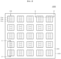
- FIG. 1 is a schematic plan view illustrating a displaying apparatus 10000 according to an exemplary embodiment
- FIG. 2 is a schematic plan view illustrating a pixel module 1000 according to an exemplary embodiment.
- the displaying apparatus 10000 is not particularly limited, but it may include a virtual reality (VR) displaying apparatus such as a micro LED TV, a smart watch, a VR headset, or an argument reality (AR) displaying apparatus such as augmented reality glasses.
- VR virtual reality
- AR argument reality
- the panel substrate 2100 may include a circuit for a passive matrix driving or active matrix driving manner.
- the panel substrate 2100 may include interconnections and resistors therein, and in another exemplary embodiment, the panel substrate 2100 may include interconnections, transistors, and capacitors.
- the panel substrate 2100 may also have pads on an upper surface thereof that may be electrically connected to the disposed circuits.
- Each of the unit pixels 100 includes a plurality of light emitting devices 10a, 10b, and 10c.
- the light emitting devices 10a, 10b, and 10c may emit light of different colors from one another.
- the light emitting devices 10a, 10b, and 10c in each of the unit pixels 100 may be arranged in a line, as illustrated in FIG. 2 .
- the light emitting devices 10a, 10b, and 10c may be arranged in a vertical direction with respect to a display screen on which an image is implemented.
- the inventive concepts are not limited thereto, and the light emitting devices 10a, 10b, and 10c may be arranged in a lateral direction with respect to the display screen on which the image is implemented.
- each element of the displaying apparatus 10000 will be described in detail in an order of the light emitting devices 10a, 10b, and 10c, the unit pixel 100, and the pixel module 1000 disposed in the displaying apparatus 10000.
- FIG. 3A is a schematic plan view illustrating the light emitting device 10a according to an exemplary embodiment
- FIG. 3B is a schematic cross-sectional view taken along line A-A' of FIG. 3A
- the light emitting device 10a is exemplarily described, but since the light emitting devices 10b and 10c have a substantially similar structure to that of the light emitting device 10a, repeated descriptions thereof will be omitted.
- the semiconductor layers may include indium gallium nitride (InGaN), gallium nitride (GaN), gallium phosphide (GaP), aluminum gallium indium phosphide (AlGaInP), or aluminum gallium phosphide (AlGaP).
- InGaN indium gallium nitride
- GaN gallium nitride
- GaP gallium phosphide
- AlGaInP aluminum gallium indium phosphide
- AlGaP aluminum gallium phosphide
- the active layer 23 may include a single quantum well structure or a multiple quantum well structure, and a composition ratio of a compound semiconductor may be adjusted to emit a desired wavelength.
- the active layer 23 may emit blue light, green light, red light, or ultraviolet light.
- the second conductivity type semiconductor layer 25 and the active layer 23 may have a mesa M structure and may be disposed on the first conductivity type semiconductor layer 21.
- the mesa M may include the second conductivity type semiconductor layer 25 and the active layer 23, and may include a portion of the first conductivity type semiconductor layer 21 as shown in FIG. 3B .
- the mesa M is located on a partial region of the first conductivity type semiconductor layer 21, and an upper surface of the first conductivity type semiconductor layer 21 may be exposed around the mesa M.
- the mesa M is formed so as to expose the first conductivity type semiconductor layer 21 around it.
- a through hole may be formed through the mesa M to expose the first conductivity type semiconductor layer 21.
- the first conductivity type semiconductor layer 21 may have a flat light exiting surface.
- the first conductivity type semiconductor layer 21 may have a concave-convex pattern formed by surface texturing on a side of the light exiting surface. Surface texturing may be carried out by patterning, for example, using a dry or wet etching process.
- cone-shaped protrusions may be formed on the light exiting surface of the first conductivity type semiconductor layer 21, a height of the cone may be about 2 ⁇ m to about 3 ⁇ m, a distance between the cones may be about 1.5 ⁇ m to about 2 ⁇ m, and a diameter of a bottom of the cone may be about 3 ⁇ m to about 5 ⁇ m.
- the cone may also be truncated, in which an upper diameter of the cone may be about 2 ⁇ m to about 3 ⁇ m.
- the concave-convex pattern may include a first concave-convex pattern and a second concave-convex pattern additionally formed on the first concave-convex pattern.
- the concave-convex pattern By forming the concave-convex pattern on the surface of the first conductivity type semiconductor layer 21, total internal reflection may be reduced, thereby increasing light extraction efficiency.
- Surface texturing may be carried out on the first conductivity type semiconductor layers of all of the first, second, and third light emitting devices 10a, 10b, and 10c, and thus, viewing angles of light emitted from the first, second, and third light emitting devices 10a, 10b, and 10c may become uniform.
- the inventive concepts are not limited thereto, and at least one of the light emitting devices 10a, 10b, and 10c may have a flat surface without including the concave-convex pattern.
- the ohmic contact layer 27 is disposed on the second conductivity type semiconductor layer 25 to be in ohmic contact with the second conductivity type semiconductor layer 25.
- the ohmic contact layer 27 may be formed of a single layer or multiple layers, and may be formed of a transparent conductive oxide film or a metal film.
- the transparent conductive oxide film may include ITO, ZnO, or the like
- the metal film may include a metal such as Al, Ti, Cr, Ni, Au, Ge, Pt, or the like and alloys thereof.
- the first contact pad 53 is disposed on the exposed first conductivity type semiconductor layer 21.
- the first contact pad 53 may be in ohmic contact with the first conductivity type semiconductor layer 21.
- the first contact pad 53 may be formed of an ohmic metal layer in ohmic contact with the first conductivity type semiconductor layer 21.
- the ohmic metal layer of the first contact pad 53 may be appropriately selected depending on a semiconductor material of the first conductivity type semiconductor layer 21.
- the first contact pad 53 may be omitted.
- the second contact pad 55 may be disposed on the ohmic contact layer 27.
- the second contact pad 55 is electrically connected to the ohmic contact layer 27.
- the second contact pad 55 may be omitted.
- the insulation layer 59 covers the mesa M, the ohmic contact layer 27, the first contact pad 53, and the second contact pad 55.
- the insulation layer 59 has openings 59a and 59b exposing the first contact pad 53 and the second contact pad 55.
- the insulation layer 59 may be formed as a single layer or multiple layers.
- the insulation layer 59 may include an insulating material such as SiO 2 , SiN x , Al 2 O 3 , and further, the insulation layer 59 may include a distributed Bragg reflector in which insulation layers having different refractive indices from one another are stacked.
- the distributed Bragg reflector may include at least two insulation layers selected from SiO 2 , Si 3 N 4 , SiON, TiO 2 , Ta 2 O 5 , Nb 2 O 5 , and MgF 2 .
- the distributed Bragg reflector reflects light emitted from the active layer 23.
- the distributed Bragg reflector may exhibit high reflectance over a relatively wide wavelength range including a peak wavelength of light emitted from the active layer 23, and may be designed in consideration of an incident angle of light.
- the distributed Bragg reflector may have a higher reflectance for light incident at an incident angle of 0 degrees than that for light incident at a different incident angle.
- the distributed Bragg reflector may have a higher reflectance for light incident at a particular incident angle than that for light incident at the incident angle of 0 degrees.
- the distributed Bragg reflector may have a higher reflectance for light incident at an incident angle of 10 degrees than that for light incident at the incident angle of 0 degrees.
- the light emitting structure of the blue light emitting device 10c has higher internal quantum efficiency compared to those of the light emitting structures of the red light emitting device 10a and the green light emitting device 10b. Accordingly, the blue light emitting device 10c may exhibit higher light extraction efficiency than those of the red and green light emitting devices 10a and 10b. As such, it may be difficult to properly maintain a color mixing ratio of red light, green light, and blue light.
- the distributed Bragg reflectors applied to the light emitting devices 10a, 10b, and 10c may be formed to have different reflectance from one another.
- the blue light emitting device 10c may have the distributed Bragg reflector having a relatively low reflectance compared to those of the red and green light emitting devices 10a and 10b.
- the distributed Bragg reflector formed in the blue light emitting device 10c may have a reflectance of 95% or less at the incident angle of 0 degrees for blue light generated in the active layer 23, and further 90% or less, the distributed Bragg reflector formed in the green light emitting device 10b may have a reflectance of about 95% or more and 99% or less at the incident angle of 0 degrees for green light, and the distributed Bragg reflector formed in the red light emitting device 10a may have a reflectance of 99% or more at the incident angle of 0 degrees for red light.
- the distributed Bragg reflectors applied to the red, green, and blue light emitting devices 10a, 10b, and 10c may have a substantially similar thickness.
- a difference in thickness between the distributed Bragg reflectors applied to these light emitting devices 10a, 10b, and 10c may be 10% or less of a thickness of a thickest distributed Bragg reflector.
- process conditions applied to the red, green, and blue light emitting devices 10a, 10b, and 10c for example, a process of patterning the insulation layer 59, may be similarly set, and furthermore, it is possible to prevent the unit pixel manufacturing process from becoming complex.
- the distributed Bragg reflectors applied to the red, green, and blue light emitting devices 10a, 10b, and 10c may have a substantially similar stacking number.
- the inventive concepts are not limited thereto.
- the different light emitting devices 10a, 10b, and 10c may include different insulation layers 59.
- the red light emitting device 10a may have the distributed Bragg reflector described above, and the green and blue light emitting devices 10b and 10c may have a single-layered insulation layer 59.
- the first electrode pad 61 and the second electrode pad 63 are disposed on the insulation layer 59.
- the first electrode pad 61 may extend from an upper region of the first contact pad 53 to an upper region of the mesa M, and the second electrode pad 63 may be disposed in the upper region of the mesa M.
- the first electrode pad 61 may be connected to the first contact pad 53 through the opening 59a, and the second electrode pad 63 may be electrically connected to the second contact pad 55.
- the first electrode pad 61 may be directly in ohmic contact with the first conductivity type semiconductor layer 21, and in this case, the first contact pad 53 may be omitted.
- the second electrode pad 63 may be directly connected to the ohmic contact layer 27.
- the first and/or second electrode pads 61 and 63 may be formed of a single layer or a multilayer metal.
- metals such as Al, Ti, Cr, Ni, Au, or the like and alloys thereof may be used.
- the first and second electrode pads 61 and 63 may include a Ti layer or a Cr layer as an upper most layer, and an Au layer thereunder.
- the light emitting device 10a may further include a layer having additional functions in addition to the above-described layers.
- a layer having additional functions such as a reflection layer for reflecting light, an additional insulation layer for insulating a specific element, and a solder preventing layer for preventing diffusion of solder may be further included.
- the mesa when a flip chip type light emitting device is formed, the mesa may be formed to have various shapes, and locations and shapes of the first and second electrode pads 61 and 63 may also be variously modified. Further, the ohmic contact layer 27 may be omitted, and the second contact pad 55 or the second electrode pad 63 may directly contact the second conductivity type semiconductor layer 25.
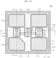
- FIG. 4A is a schematic plan view illustrating a unit pixel 100 according to an exemplary embodiment
- FIG. 4B is a schematic cross-sectional view taken along line B-B' of FIG. 4A
- FIG. 4C is a schematic cross-sectional view taken along line C-C' of FIG. 4A .
- the unit pixel 100 may include a transparent substrate 121, first, second, and third light emitting devices 10a, 10b, and 10c, a surface layer 122, a light blocking layer 123, an adhesive layer 125, a step adjustment layer 127, connection layers 129a, 129b, 129c, and 129d, and an insulation material layer 131.
- the unit pixel 100 provides a single pixel including the first, second, and third light emitting devices 10a, 10b, and 10c.
- the first, second, and third light emitting devices 10a, 10b, and 10c emit light of different colors, and the first, second, and third light emitting devices 10a, 10b, and 10c correspond to subpixels, respectively.
- the transparent substrate 121 is a light transmissive substrate such as PET, glass substrate, quartz, sapphire substrate, or the like.
- the transparent substrate 121 is disposed on a light exiting surface of the displaying apparatus (10000 in FIG. 1 ), and light emitted from the light emitting devices 10a, 10b, and 10c is emitted to the outside through the transparent substrate 121.
- the transparent substrate 121 may have an upper surface and a lower surface.
- the transparent substrate 121 may include a concave-convex pattern 121p on a surface facing the light emitting devices 10a, 10b, and 10c, that is, the upper surface.
- the concave-convex pattern 121p scatters light emitted from the light emitting devices 10a, 10b, and 10c to increase a viewing angle.
- light emitted from the light emitting devices 10a, 10b, and 10c having different viewing angle characteristics from one another may be emitted at a uniform viewing angle by the concave-convex pattern 121p. As such, it is possible to prevent an occurrence of color difference depending on the viewing angle.
- the concavo-convex pattern 121p may be regular or irregular.
- the concavo-convex pattern 121p may have a pitch of about 3 ⁇ m, a diameter of about 2.8 ⁇ m, and a height of about 1.8 ⁇ m, for example.
- the concavo-convex pattern 121p may be a pattern generally applied to a patterned sapphire substrate, but the inventive concepts are not limited thereto.
- the transparent substrate 121 may also include an anti-reflection coating, may include an anti-glare layer, or may be treated with an anti-glare treatment.
- the transparent substrate 121 may have a thickness of about 50 ⁇ m to about 300 ⁇ m for example.
- the transparent substrate 121 Since the transparent substrate 121 is disposed on the light exiting surface, the transparent substrate 121 does not include a circuit. However, the inventive concepts are not limited thereto, and, in some exemplary embodiments, the transparent substrate 121 may include the circuit.
- a single unit pixel 100 is illustrated to be formed on a single transparent substrate 121, a plurality of unit pixels 100 may be formed on the single transparent substrate 121.
- the surface layer 122 covers the concave-convex pattern 121p of the transparent substrate 121.
- the surface layer 122 may be formed along a shape of the concave-convex pattern 121p.
- the surface layer 122 may improve adhesion of the light blocking layer 123 formed thereon.
- the surface layer 122 may be formed of a silicon oxide layer.
- the surface layer 122 may be omitted depending on a type of the transparent substrate 121.
- the light blocking layer 123 is formed on the upper surface of the transparent substrate 121.
- the light blocking layer 123 may contact the surface layer 122.
- the light blocking layer 123 may include an absorbing material which absorbs light such as carbon black. The light absorbing material may prevent light generated in the light emitting devices 10a, 10b, and 10c from leaking from a region between the transparent substrate 121 and the light emitting devices 10a, 10b, and 10c toward a side surface thereof, and may improve contrast of the displaying apparatus.
- the light blocking layer 123 may have windows 123a, 123b, and 123c for a light path, so that light generated in the light emitting devices 10a, 10b, and 10c is incident on the transparent substrate 121, and for this purpose, the light blocking layer 123 may be patterned so as to expose the transparent substrate 121 on the transparent substrate 121. Widths of the windows 123a, 123b, and 123c may be narrower than those of the light emitting devices, but the inventive concepts are not limited thereto.
- the widths of the windows 123a, 123b, and 123c may be greater than those of the light emitting devices 10a, 10b, and 10c, and thus, a gap may be formed between the light emitting device 10a and the light blocking layer 123.
- the first, second, and third light emitting devices 10a, 10b, and 10c are disposed on the transparent substrate 121.
- the first, second, and third light emitting devices 10a, 10b, and 10c may be attached to the transparent substrate 121 by the adhesive layer 125.
- the first, second, and third light emitting devices 10a, 10b, and 10c may be disposed corresponding to the windows 123a, 123b, and 123c of the light blocking layer 123.
- the first, second, and third light emitting devices 10a, 10b, and 10c may be disposed on a flat surface of the adhesive layer 125 as shown in FIGS. 4B and 4C .
- the adhesive layer 125 may be disposed under lower surfaces of the light emitting devices 10a, 10b, and 10c. In another exemplary embodiment, the adhesive layer 125 may partially cover side surfaces of the first, second, and third light emitting devices 10a, 10b, and 10c.
- the first, second, and third light emitting devices 10a, 10b, and 10c may be, for example, a red light emitting device, a green light emitting device, and a blue light emitting device. Since a detailed configuration of each of the first, second, and third light emitting devices 10a, 10b, and 10c is the same as described above with reference to FIGS. 3A and 3B , a detailed description thereof will be omitted.
- the first, second, and third light emitting devices 10a, 10b, and 10c may be arranged in a line, as illustrated in FIG. 4A .
- the transparent substrate 121 is a sapphire substrate
- the sapphire substrate may include clean-cut surfaces (e.g., m-plane) and non clean-cut surfaces (e.g., a-plane) due to a location of a crystal plane along a cutting direction.
- the sapphire substrate when the sapphire substrate is cut into a quadrangular shape, two cutting planes on both sides thereof (e.g., m-plane) may be cut cleanly along the crystal plane, and two remaining cutting planes (e.g., a-plane) disposed in a direction perpendicular to the cutting planes may not be cut cleanly.
- the clean-cut surfaces of the sapphire substrate 121 may be flush with an arrangement direction of the light emitting devices 10a, 10b, and 10c.
- the clean-cut surfaces e.g., m-plane
- the two remaining cut surfaces e.g., a-plane
- each of the first, second, and third light emitting devices 10a, 10b, and 10c may be arranged in parallel to one another in a major axis direction. Minor axis directions of the first, second, and third light emitting devices 10a, 10b, and 10c may coincide with an arrangement direction of the light emitting devices.
- the first, second, and third light emitting devices 10a, 10b, and 10c may have been those described above with reference to FIGS. 3A and 3B , but the inventive concepts are not limited thereto, and various light emitting devices of a lateral type or a flip-chip structure may be used.
- the step adjustment layer 127 may be disposed in a region surrounded by an edge of the adhesive layer 125, but the inventive concepts are not limited thereto.
- the step adjustment layer 127 may be formed to partially expose the edge of the adhesive layer 125.
- connection layers 129a, 129b, 129c, and 129d are formed on the step adjustment layer 127.
- the connection layers 129a, 129b, 129c, and 129d may be connected to the first and second electrode pads 61 and 63 of the first, second, and third light emitting devices 10a, 10b, and 10c through the openings 127a of the step adjustment layer 127.
- the insulation material layer 131 may be formed to have a thickness smaller than that of the step adjustment layer 127.
- a sum of the thicknesses of the insulation material layer 131 and the step adjustment layer 127 may be about 1 ⁇ m or more and about 50 ⁇ m or less, but the inventive concepts are not limited thereto.
- a side surface of the insulation material layer 131 may have an inclination angle less than 90 degrees with respect to the upper surface of the adhesive layer 125, for example, an inclination angle of about 60 degrees.
- the insulation material layer 131 may be a translucent material, and may be formed of an organic or inorganic material.
- the insulation material layer 131 may be formed of, for example, polyimide.
- the insulation material layer 131 along with the step adjustment layer 127 is formed of polyimide, all of lower, side, and upper surfaces of the connection layers 129a, 129b, 129c, and 129d may be surrounded by the polyimide, except for the pad regions.
- the unit pixel 100 does not include separate bumps, and the connection layers 129a, 129b, 129c, and 129d are used as bonding pads.
- the inventive concepts are not limited thereto, and bonding pads covering the openings 131a, 131b, 131c, and 131d of the insulation material layer 131 may be formed.
- the bonding pads may be formed to partially cover the light emitting devices 10a, 10b, and 10c outside of upper regions of the first, second, third, and fourth connection layers 129a, 129b, 129c, and 129d.
- the optical layer is formed of a material such as gas, liquid, or solid, different from those of the light emitting devices 10a, 10b, and 10c, and thus, is distinguished from the materials of the semiconductor layers in the light emitting devices 10a, 10b, and 10c.
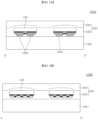
- FIG. 5A is a schematic partial cross-sectional view taken along line D-D' of FIG. 2 to illustrate the pixel module 1000 according to an exemplary embodiment
- FIG. 5B is a schematic partial cross-sectional view taken along line E-E' of FIG. 2 .
- the pixel module 1000 includes the circuit board 1001 and the unit pixels 100 arranged on the circuit board 1001. Furthermore, the pixel module 1000 may further include the molding member 200 covering the unit pixels 100.
- the unit pixels 100 may be arranged on the circuit board 1001.
- the unit pixels 100 may be arranged in various matrices, such as 2 ⁇ 2, 2 ⁇ 3, 3 ⁇ 3, 4 ⁇ 4, 5 ⁇ 5, and the like.
- the unit pixels 100 may be bonded to the circuit board 1001 through a bonding material 1005.
- the bonding material 1005 bonds connection layers 129a, 129b, 129c, and 129d exposed through the openings 131a, 131b, 131c, and 131d of the insulation material layer 131 described with reference to FIGS. 4A , 4B, and 4C to pads 1003.
- the bonding material 1005 having a single structure may be disposed between the connection layers 129a, 129b, 129c, and 129d and the pads 1003, and the bonding material 1005 may directly connect the connection layers 129a, 129b, 129c, and 129d and the pads 1003
- the light diffusion layer 230 may have, for example, a thickness within a range of about 25 ⁇ m to about 200 ⁇ m, and the light diffusion particles may be included in thelight diffusion layer 230, for example, within a range of about 0.2 wt% to 10 wt% based on a total weight of thelight diffusion layer 230.
- the light diffusion layer 230 scatters light emitted from the light emitting devices 10a, 10b, and 10c.
- the light diffusion layer 230 assists to uniformly mix light of different colors emitted from the unit pixel 100, and also prevents light emitted to a side surface of the unit pixel 100 from being emitted to the outside.
- the black molding layer 250 includes a material that absorbs light in a matrix.
- the matrix may be, for example, a dry-film type solder resist (DFSR), photoimageable solder resist (PSR), an epoxy molding compound (EMC), or the like, without being limited thereto.
- the light absorbing material may include a light absorbing dye such as carbon black.
- the light absorbing dye may be directly dispersed in the matrix, or may be coated on surfaces of organic or inorganic particles to be dispersed in the matrix.
- Various types of organic or inorganic particles may be used so as to coat the light absorbing material. For example, particles coated with TiO 2 or silica particles with carbon black may be used.
- the black molding layer 250 may be formed to have a thickness within a range of about 25 ⁇ m to about 200 ⁇ m.
- a light transmittance may be adjusted by adjusting a concentration of the light absorbing material contained in the molding member 200.
- the light absorbing material may within a range of about 0.05 wt% to about 10 wt% relative to a total matrix weight.
- the black molding layer 250 may be formed as a single layer in which the light absorbing material is uniformly dispersed, but the inventive concepts are not limited thereto.
- the black molding layer 250 may be formed of a plurality of layers having different concentrations of the light absorbing material.
- the black molding layer 250 may include two layers having different concentrations of the light absorbing material.
- a first layer disposed closer to the light diffusion layer 230 may contain more light absorbing material than a second layer.
- a total absorption of light emitted upward from the unit pixel 100 may be reduced by making a light absorptivity of the first layer higher than that of the second layer, and thus, luminance of the pixel module 1000 may be increased.
- the layers when the black molding layer 250 is formed of the plurality of layers, the layers may be clearly distinguished from one another.
- the black molding layer 250 may be manufactured by sandwiching the films.
- the black molding layer 250 may be formed by continuously printing the layers having different concentrations of the light absorbing material.
- the black molding layer 250 may be formed such that the concentration of the light absorbing material gradually decreases in a thickness direction thereof.
- the light diffusion layer 230 may have a convex upper surface
- the black molding layer 250 may have a flat upper surface compared to that of the light diffusion layer 230.
- the thickness of the light diffusion layer 230 may vary along a lateral direction of the circuit board 1001.
- the light diffusion layer 230 may have a relatively smaller thickness in the upper region of the unit pixels 100 than in the region between the unit pixels 100.
- the thickness of the black molding layer 250 may also vary along the lateral direction of the circuit board 1001.
- the black molding layer 250 may have a relatively smaller thickness in the upper region of the unit pixels 100 than in the region between the unit pixels 100.
- the black molding layer 250 By forming the black molding layer 250 relatively thick in the region between the unit pixels 100 and forming the black molding layer 250 relatively thin in the upper region of the unit pixels 100, it is possible to increase an efficiency of light emitted upward from the unit pixels 100 and to further improve a contrast by blocking light incident with an inclination angle.
- a displaying apparatus 10000 may be provided by mounting the plurality of pixel modules 1000 shown in FIGS. 5A and 5B on the panel substrate 2100 of FIG. 1 .
- the circuit board 1001 has bottom pads connected to the pads 1003.
- the bottom pads may be disposed to correspond one-to-one to the pads 1003, but the number of the bottom pads may be reduced through a common connection.
- the displaying apparatus 10000 since the unit pixels 100 are formed into the pixel module 1000, and the pixel modules 1000 are mounted on the panel substrate 2100, the displaying apparatus 10000 may be provided, and thus, a process yield of the displaying apparatus may be improved.
- the inventive concepts are not limited thereto, and the unit pixels 100 may be directly mounted on the panel substrate 2100.
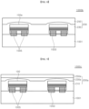
- the pixel module 1000a is substantially similar to the pixel module 1000 described with reference to FIGS. 5A and 5B , except that a molding member 200a includes a transparent molding layer 210, a light diffusion layer 230a, and a black molding layer 250a.
- the transparent molding layer 210 is formed of a transparent material such as an epoxy molding compound.
- the light diffusion layer 230a is disposed on the transparent molding layer 210, and the black molding layer 250a is disposed on the light diffusion layer 230a. Since the light diffusion layer 230a and the black molding layer 250a are similar to the light diffusion layer 230 and the black molding layer 250 described above, a detailed description of a same element will be omitted to avoid redundancy.
- a total thickness of the molding member 200a may be in a range of about 50 ⁇ m to about 400 ⁇ m, the transparent molding layer 210 in a range of about 20 ⁇ m to about 150 ⁇ m, the light diffusion layer 230a in a range of about 15 ⁇ m to about 150 ⁇ m, the black molding layer 250a in a range of about 15 ⁇ m to about 150 ⁇ m.
- the thickness of the black molding layer 250a in the upper region of the unit pixels 100 may be greater than the thickness of the transparent molding layer 210 and/or the thickness of the light diffusion layer 230a, without being limited thereto.
- the thickness of the black molding layer 250a may be smaller than the thickness of the transparent molding layer 210 or the thickness of the light diffusion layer 230a.
- the thickness of the transparent molding layer 210 may be greater than the thickness of the light diffusion layer 230a.
- the transparent molding layer 210 may have a convex upper surface, and the light diffusion layer 230a and the black molding layer 250a may have a flat upper surface compared to the transparent molding layer 210.
- the upper surface of the light diffusion layer 230a is illustrated as being flat, the upper surface of the light diffusion layer 230a may also have a convex shape, and the upper surface of the black molding layer 250a may be relatively flatter than the upper surface of the light diffusion layer 230a.
- the thickness of the transparent molding layer 210 increases, the thickness of the convex portion of the transparent molding layer 210 in the upper region of the unit pixels 100 increases.
- the thicknesses of the transparent molding layer 210 and the light diffusion layer 230a may vary along the lateral direction of the circuit board 1001.
- the transparent molding layer 210 and the light diffusion layer 230a may have a relatively smaller thickness in the upper region of the unit pixels 100 than in the region between the unit pixels 100.
- the thickness of the black molding layer 250a may not substantially change along the lateral direction of the circuit board 1001.
- the present disclosure is not limited thereto, and the black molding layer 250a may also have a relatively smaller thickness in the upper region of the unit pixels 100 than in the region between the unit pixels 100.
- the unit pixel 100a has a structure in which first, second, and third light emitting stacks 320, 330, and 340 are stacked, unlike the unit pixel 100 described with reference to FIGS. 4A , 4B, and 4C .
- the unit pixel 100a includes a light emitting stacked structure, a first connection electrode 350a, a second connection electrode 350b, a third connection electrode 350c, and a fourth connection electrode 350d formed on the light emitting stacked structure; and a passivation layer 390 surrounding the connection electrodes 350a, 350b, 350c, and 350d.
- the unit pixel 100a may also include a substrate 311.
- the light emitting stacked structure may include the first light emitting stack 320, the second light emitting stack 330, and the third light emitting stack 340.
- the inventive concepts are not limited to a specific number of light emitting stacks.
- the light emitting stacked structure may include two or more light emitting stacks.
- the unit pixel 100a includes the three light emitting stacks 320, 330, and 340 according to an exemplary embodiment.
- the substrate 311 may be a light transmissive insulating substrate. However, in some exemplary embodiments, the substrate 311 may be formed to be translucent or partially transparent so as to transmit only light of a specific wavelength or transmit only a portion of light of a specific wavelength.
- the substrate 311 may be a growth substrate on which the first light emitting stack 320 may be epitaxially grown, for example, a sapphire substrate. However, the substrate 311 is not limited to the sapphire substrate, and may include various other transparent insulating materials.
- the substrate 311 may include a glass, a quartz, a silicon, an organic polymer, or an organic-inorganic composite material, and may be, for example, such as silicon carbide (SiC), gallium nitride (GaN), indium gallium nitride (InGaN), aluminum gallium nitride (AlGaN), aluminum nitride (AlN), gallium oxide (Ga2O3), or a silicon substrate.
- the substrate 311 may include irregularities on an upper surface thereof, and may be, for example, a patterned sapphire substrate. By including the irregularities on the upper surface, extraction efficiency of light generated in the first light emitting stack 320 in contact with the substrate 311 may be increased.
- the irregularities of the substrate 311 may be employed so as to selectively increase a luminous intensity of the first light emitting stack 320 compared to the second light emitting stack 330 and the third light emitting stack 340.
- the first, second, and third light emitting stacks 320, 330, and 340 are configured to emit light towards the substrate 311. Accordingly, light emitted from the third light emitting stack 340 may pass through the first and second light emitting stacks 320 and 330. According to an exemplary embodiment, the first, second, and third light emitting stacks 320, 330, and 340 may emit light of different peak wavelengths from one another. In general, since the light emitting stack disposed farther from the substrate 311 emits light of a longer wavelength than that of the light emitting stack disposed near the substrate 311, a light loss may be reduced.
- the second light emitting stack 330 may emit light of a shorter wavelength than that of the first LED stack 320. Accordingly, it is possible to reduce the luminous intensity of the second light emitting stack 330 and increase the luminous intensity of the first LED stack 320, and thus, it is possible to dramatically change a luminous intensity ratio of light emitted from the first, second, and third light emitting stacks.
- the first light emitting stack 320 may be configured to emit green light
- the second light emitting stack 330 to emit blue light
- the third light emitting stack 340 to emit red light.
- an emission area of the first, second, and third LED stacks 320, 330, and 340 may be less than or equal to about 10000 um 2 , further, may be less than or equal to 4000 um 2 , furthermore, less than or equal to 2500 um 2 .
- the emission area may be increased with decreasing distance to the substrate 311, and the luminous intensity of green light may be further increased by disposing the first LED stack 320 emitting green light closest to the substrate 311.
- the first to third light emitting stacks 320, 330, and 340 include, as those described with reference to FIGS. 3A and 3B , a first conductivity type semiconductor layer 21, an active layer 23, and a second conductivity type semiconductor layer 25, respectively.
- the first light emitting stack 320 may include a semiconductor material emitting green light, such as GaN, InGaN, GaP, AlGaInP, AlGaP, or the like.
- the second light emitting stack 330 may include a semiconductor material emitting blue light, such as GaN, InGaN, ZnSe, or the like, without being limited thereto.
- the third light emitting stack 340 may include, for example, a semiconductor material emitting red light such as AlGaAs, GaAsP, AlGaInP, GaP, or the like, without being limited thereto.
- each of the first conductivity type semiconductor layers 21 and the second conductivity type semiconductor layers 25 of the first, second, and third light emitting stacks 320, 330, and 340 may have a single-layered structure or a multi-layered structure and, in some exemplary embodiments, may include a superlattice layer. Furthermore, the active layers 23 of the first, second, and third light emitting stacks 320, 330, and 340 may have a single quantum well structure or a multiple quantum well structure.
- a first adhesive layer 325 is disposed between the first light emitting stack 320 and the second light emitting stack 330, and a second adhesive layer 335 is disposed between the second light emitting stack 330 and the third light emitting stack 340.
- the first and second adhesive layers 325 and 335 may include a non-conductive material that transmits light.
- the first and second adhesive layers 325 and 335 may include an optically clear adhesive (OCA), which may include epoxy, polyimide, SU8, spin-on-glass (SOG), benzocyclobutene (BCB), without being limited thereto.
- OCA optically clear adhesive
- each of the first, second, and third light emitting stacks 320, 330 and 340 may be driven independently. More specifically, a common voltage may be applied to one of the first and second conductivity type semiconductor layers of each of the light emitting stacks, and an individual light emitting signal may be applied to another one of the first and second conductivity type semiconductor layers of each of the light emitting stacks.
- the first conductivity type semiconductor layer 21 of each of the light emitting stacks may be n-type
- the second conductivity type semiconductor layer 25 may be p-type.
- the n-type semiconductor layer and the p-type semiconductor layer may be arranged in a same sequence, but the inventive concepts are not limited thereto.
- the first light emitting stack 320 may have a reversely stacked sequence compared to those of the second light emitting stack 330 and the third light emitting stack 340.
- the first, second, and third light emitting stacks 320, 330, and 340 may have a common p-type light emitting stacked structure in which the p-type semiconductor layers are commonly electrically connected, or may have a common n-type light emitting stacked structure in which the n-type semiconductor layers are commonly electrically connected.
- each of the connection electrodes 350a, 350b, 350c, and 350d may have a substantially elongated shape protruding from the substrate 311.
- the connection electrodes 350a, 350b, 350c, and 350d may include a metal such as Cu, Ni, Ti, Sb, Zn, Mo, Co, Sn, Ag, or an alloy thereof, without being limited thereto.
- each of the connection electrodes 350a, 350b, 350c, and 350d may include two or more metals or a plurality of different metallic layers so as to reduce stress from the elongated shape of the connection electrodes 350a, 350b, 350c, and 350d.
- connection electrodes 350a, 350b, 350c, and 350d include Cu
- an additional metal may be deposited or plated to suppress oxidation of Cu.
- connection electrodes 350a, 350b, 350c, and 350d include Cu/Ni/Sn
- Cu may prevent Sn from infiltrating into the light emitting stacked structure.
- the connection electrodes 350a, 350b, 350c, and 350d may include a seed layer for forming a metallic layer during a plating process, which will be described later.
- each of the connection electrodes 350a, 350b, 350c, and 350d may have a substantially flat upper surface, and thus, an electrical connection between an external line or an electrode and the light emitting stacked structure may be facilitated, which will be described later.
- the connection electrodes 350a, 350b, 350c, and 350d may overlap a portion of at least one of the first, second, and third light emitting stacks 320, 330, and 340 as shown in the drawings.
- connection electrodes 350a, 350b, 350c, and 350d are illustrated as having a quadrangular pillar shape, but the present disclosure is not limited thereto, and may have a cylindrical shape. Furthermore, areas of lower surfaces of the connection electrodes 350a, 350b, 350c, and 350d may be larger than those of the upper surfaces thereof. For example, when the first to third light emitting stacks 320, 330, and 340 are patterned so as to form electrodes, the connection electrodes 350a, 350b, 350c and 350d may cover side surfaces of the first to third light emitting stacks 320, 330, and 340.
- an array of a plurality of unit pixels 100a is formed on the substrate 311.
- the substrate 311 may be cut along scribing lines to be singularized (isolated) into each unit pixel 100a, and the unit pixel 100a may be transferred to another substrate or tape using various transferring techniques.
- the unit pixel 100a includes the connection electrodes 350a, 350b, 350c, and 350d such as metallic bumps or pillars protruding outward
- various drawbacks may occur during subsequent processes, for example, in a transferring step, due to the structure in which the connection electrodes 350a, 350b, 350c, and 350d are exposed to the outside.
- the unit pixel 100a includes a micro-LED, which has a surface area less than about 10,000 ⁇ m 2 , or less than about 4,000 ⁇ m 2 , or less than about 2,500 ⁇ m 2 , depending upon applications, handling of the unit pixel 100a may become more difficult due to its small form factor.
- connection electrodes 350a, 350b, 350c, and 350d have a substantially elongated shape such as a rod
- transferring the unit pixel 100a using a conventional vacuum method is difficult due to a protruding structure of the connection electrode due to an insufficient suction area.
- the exposed connection electrode may be directly affected by various stresses during subsequent processes, such as when the connection electrode is in contact with a manufacturing device, which may damage the structure of the unit pixel 100a.
- a contact area between the unit pixel 100a and the adhesive tape may be limited to the upper surfaces of the connection electrodes 350a, 350b, 350c, and 350d when the unit pixel 100a is transferred.
- an adhesive force of the unit pixel 100a to the adhesive tape may be weakened, and the unit pixel 100a may be undesirably separated from the adhesive tape during transferring.
- an ejection pin may directly contact a portion of the unit pixel 100a and damage a top structure of the light emitting structure.
- the ejection pin may strike a center of the unit pixel 100a, and cause physical damage to the top light emitting stack of the unit pixel 100a.
- the passivation layer 390 may at least partially cover the side surfaces of the first to third light emitting stacks 320, 330, and 340, and the side surfaces of the first to third light emitting stacks 320, 330, and 340 may not be exposed to the outside of the unit pixel 100a by being covered with the passivation layer 390 and another insulation layer.
- the passivation layer 390 may be formed substantially flush with the upper surfaces of the connection electrodes 350a, 350b, 350c, and 350d.
- the passivation layer 390 may include an epoxy molding compound (EMC), which may be formed in various colors such as black, white, or transparent.
- EMC epoxy molding compound
- the inventive concepts are not limited thereto.
- the passivation layer 390 may include polyimide (PID), and in this case, the PID may be provided as a dry film rather than a liquid type so as to increase a level of flatness when applied to the light emitting stacked structure.
- the passivation layer 390 may include a photosensitive material.
- FIG. 8 is a schematic cross-sectional view illustrating a pixel module 1000b according to another exemplary embodiment.
- the pixel module 1000b is substantially similar to the pixel module 1000 described with reference to FIGS. 5A and 5B , except that a unit pixel 100a is used instead of the unit pixel 100.
- FIG. 9 is a schematic cross-sectional view illustrating a pixel module 1000c according to another exemplary embodiment.
- the pixel module 1000c is substantially similar to the pixel module 1000b described with reference to FIG. 8 , except that a molding member 200a is used instead of the molding member 200. Since the molding member 200a is the same as described above with reference to FIGS. 6A and 6B , a detailed description thereof will be omitted to avoid redundancy.
- Connection electrodes of the unit pixel 100a are bonded to the pads 1003 on the circuit board 1001. As shown in FIGS. 5A and 5B , the bonding material 1005 may be disposed between the connection electrodes and the pads 1003.
- a light diffusion layer 230 and a black molding layer 250 are constricted.
- Each of the light diffusion layer 230 and the black molding layer 250 may be formed in a form of a film, and these films may be bonded in close contact with each other.
- Each of the light diffusion layer 230 and the black molding layer 250 may be manufactured in the form of the film using applying and drying techniques on a temporary substrate.
- the light diffusion layer 230 and the black molding layer 250 described with reference to FIG. 10A cover the unit pixels 100 through a vacuum lamination process. Accordingly, a molding member 200 covering the unit pixels 100 is formed.
- the light diffusion layer 230 located in an upper portion of the unit pixel 100 may have a convex shape, as shown in FIG. 10C .
- An upper surface of the black molding layer 250 may have a flat surface, and thus, a thickness of the black molding layer 250 located in the upper portion of the unit pixel 100 may be smaller than a thickness of the black molding layer 250 located between the unit pixels 100.
- the transparent molding layer 210 located in the upper portion of the unit pixel 100 may have a convex shape, and the light diffusion layer 230a and the black molding layer 250a may have a flat upper surface.
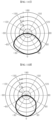
- FIGS. 11A, 11B , 11C, 11D , and 11E are graphs illustrating a normalized light distribution of a pixel module according to structures of various molding members.
- the pixel modules were manufactured using unit pixels of a same stacked structure, except that molding structures were different from one another. Molding members of Comparative Example 2, Comparative Example 3, Inventive Example 1, and Inventive Example 2 below were all formed using a vacuum lamination process. For each sample, it can be judged as favorable that a viewing angle is less than 120 degrees, and a maximum value of ⁇ u'v' in a range of left and right +-45 degree is less than 0.01.
- Inventive Example 1 150 ⁇ m of a light diffusion layer containing about 0.7 wt% of TiO 2 particles and 50 ⁇ m of a black molding layer containing 0.2 wt% of carbon black were used, and in Inventive Example 2 ( FIG. 11E ), 150 ⁇ m of a light diffusion layer containing about 1.0 wt% of TiO 2 particles and 50 ⁇ m of a black molding layer containing 0.2 wt% of carbon black were used.
- Comparative Example 2 ( FIG. 11B ), a viewing angle was about 132.0 degrees which is smaller compared to that of Comparative Example 1 in which the molding member was not formed, and a maximum ⁇ u'v' at +-45 degrees was 0.023 which was smaller than that of Comparative Example 1, but a color deviation thereof was still quite high.
- Comparative Example 3 ( FIG. 11C ) had a viewing angle of about 131.4 degrees, and a maximum ⁇ u'v' at +-45 degrees was 0.018, which was improved compared to Comparative Example 2, but the viewing angle was still relatively wide and a color deviation thereof was quite high.
- Inventive Example 2 ( FIG. 11E ) had a viewing angle of about 110.9 degrees, and a maximum ⁇ u'v' at +-45 degrees was 0.006, which had significantly improved viewing angle and color deviation compared to those of Comparative Examples 1 to 3.
- the maximum ⁇ u'v' at +-45 degrees indicating color deviation is less than 0.01, and thus, it can be seen that the color deviation is significantly reduced.
- the viewing angle and the color deviation may be reduced by using the molding member including the light diffusion layer and the black molding layer.
Landscapes
- Led Device Packages (AREA)
- Electroluminescent Light Sources (AREA)
- Devices For Indicating Variable Information By Combining Individual Elements (AREA)
Abstract
Description
- Exemplary embodiments relate to a displaying apparatus, and more particularly, to a pixel module employing a molding member having a multi-molding layer and a displaying apparatus having the same.
- Light emitting devices are semiconductor devices using light emitting diodes which are inorganic light sources, and are used in various technical fields such as displaying apparatuses, automobile lamps, general lighting, and the like. Light emitting diodes have advantages such as longer lifespan, lower power consumption, and quicker response, than conventional light sources, and thus, the light emitting diodes have been replacing the conventional light sources.
- Conventional light emitting diodes have been generally used as backlight light sources in displaying apparatuses, but displaying apparatuses that directly realize images using the light emitting diodes have been recently developed. Such displays are also referred to as micro LED displays.
- In general, the displaying apparatus realizes various colors using a mixed color of blue, green, and red. The displaying apparatus includes a plurality of pixels in order to realize various images, each including sub-pixels corresponding to one of blue, green, and red light. As such, a color of a certain pixel is typically determined based on the colors of the sub-pixels, so that images can be realized through the combination of such pixels.
- In a case of the micro LED display, a micro LED is arranged on a two-dimensional plane corresponding to each sub pixel, and, accordingly, a large number of micro LEDs need to be arranged on a single substrate. However, the micro LED is extremely small, for example, 200 µm or less, further 100 µm or less, and these small sizes cause various drawbacks. In particular, it is difficult to handle the light emitting diodes having small sizes, and thus, it is not easy to directly mount the light emitting diodes on a display panel.
- Meanwhile, light interference between adjacent sub-pixels makes it difficult to achieve high color reproducibility and high contrast. Moreover, it is required to reduce a color deviation depending on a viewing angle.
- Exemplary embodiments provide a pixel module capable of reducing a color deviation depending on a viewing angle, and a displaying apparatus having the same.
- Exemplary embodiments provide a pixel module capable of preventing light interference to achieve high color reproducibility, and a displaying apparatus having the same.
- A pixel module according to one or more exemplary embodiments of the present disclosure includes a circuit board, unit pixels arranged on the circuit board, and a molding member covering the unit pixels. The molding member includes a light diffusion layer and a black molding layer covering the light diffusion layer.
- A displaying apparatus according to one or more exemplary embodiments of the present disclosure includes a panel substrate and a plurality of pixel modules disposed on the panel substrate. Each of the pixel modules includes a circuit board, unit pixels arranged on the circuit board, and a molding member covering the unit pixels. The molding member includes a light diffusion layer and a black molding layer covering the light diffusion layer.
-
-
FIG. 1 is a schematic plan view illustrating a displaying apparatus according to an exemplary embodiment. -
FIG. 2 is a schematic plan view illustrating a pixel module according to an exemplary embodiment. -
FIG. 3A is a schematic plan view illustrating a light emitting device according to an exemplary embodiment. -
FIG. 3B is a schematic cross-sectional view taken along line A-A' ofFIG. 3A . -
FIG. 4A is a schematic plan view illustrating a unit pixel according to an exemplary embodiment. -
FIG. 4B is a schematic cross-sectional view taken along line B-B' ofFIG. 4A . -
FIG. 4C is a schematic cross-sectional view taken along line C-C' ofFIG. 4A . -
FIG. 5A is a schematic partial cross-sectional view taken along line D-D' ofFIG. 2 to illustrate the pixel module according to an exemplary embodiment. -
FIG. 5B is a schematic partial cross-sectional view taken along line E-E' ofFIG. 2 to illustrate the pixel module according to an exemplary embodiment. -
FIG. 6A and FIG. 6B are schematic partial cross-sectional views taken along line D-D' and E-E' ofFIG. 2 to illustrate a pixel module according to an exemplary embodiment. -
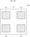
FIG. 7A is a schematic cross-sectional view illustrating a unit pixel according to another exemplary embodiment. -
FIG. 7B is a schematic plan view illustrating the unit pixel according to another exemplary embodiment. -
FIG. 8 is a schematic partial cross-sectional view illustrating a pixel module according to an exemplary embodiment. -
FIG. 9 is a schematic partial cross-sectional view illustrating a pixel module according to another exemplary embodiment. -
FIGS. 10A, 10B, and 10C are schematic cross-sectional views illustrating a method of manufacturing a pixel module according to an exemplary embodiment. -
FIGS. 11A, 11B ,11C, 11D , and11E are graphs illustrating normalized light distribution of a pixel module according to structures of various molding members. - Hereinafter, exemplary embodiments of the present disclosure will be described in detail with reference to the accompanying drawings. The following exemplary embodiments are provided by way of example so as to fully convey the spirit of the present disclosure to those skilled in the art to which the present disclosure pertains. Accordingly, the present disclosure is not limited to the embodiments disclosed herein and can also be implemented in different forms. In the drawings, widths, lengths, thicknesses, and the like of elements can be exaggerated for clarity and descriptive purposes. When an element or layer is referred to as being "disposed above" or "disposed on" another element or layer, it can be directly "disposed above" or "disposed on" the other element or layer or intervening elements or layers can be present. Throughout the specification, like reference numerals denote like elements having the same or similar functions.
- A pixel module according to one or more exemplary embodiments of the present disclosure includes a circuit board, unit pixels arranged on the circuit board, and a molding member covering the unit pixels. The molding member includes a light diffusion layer and a black molding layer covering the light diffusion layer.
- The light diffusion layer may include a transparent matrix and silica or TiO2 particles in the transparent matrix.
- The black molding layer may include a matrix and a light absorbing material in the matrix.
- Furthermore, the light absorbing material may include carbon black.
- The carbon black may be coated on surfaces of organic or inorganic particles.
- The inorganic particles may include silica or TiO2.
- In an exemplary embodiment, the black molding layer may include a plurality of layers having different concentrations of the light absorbing material.
- A layer with a higher concentration of light absorbing material may be disposed further apart from the light diffusion layer.
- In another exemplary embodiment, a concentration of the light absorbing material in the black molding layer may be gradually decreased from the light diffusion layer in a thickness direction of the black molding layer.
- The molding member may further include a transparent molding layer disposed between the unit pixel and the light diffusion layer.
- The unit pixel may include at least three light emitting devices disposed adjacent to one another.
- Furthermore, the unit pixel may further include a step adjustment layer disposed between the light emitting devices.
- A thickness of at least one of the light diffusion layer and the black molding layer may vary along a lateral direction of the circuit board.
- The black molding layer may have a smaller thickness in an upper region of the unit pixel than in a region between the unit pixels.
- An upper surface of the protection layer and upper surfaces of the connection electrodes may be flush with one another.
- The molding member may have a thickness within a range of 50 µm to 400 µm.
- Furthermore, the molding member may be formed through a vacuum lamination technique using a film including the light diffusion layer and the black molding layer.
- The pixel module may have a viewing angle of 120 degrees or less, and a maximum Δu'v' may not exceed 0.01 in a range of +-45 degrees.
- A displaying apparatus according to one or more exemplary embodiments of the present disclosure includes a panel substrate and a plurality of pixel modules disposed on the panel substrate. Each of the pixel modules includes a circuit board, unit pixels arranged on the circuit board, and a molding member covering the unit pixels. The molding member includes a light diffusion layer and a black molding layer covering the light diffusion layer.
- The molding member may further include a transparent molding layer disposed between the unit pixel and the light diffusion layer.
- Hereinafter, exemplary embodiments of the present disclosure will be described in more detail with reference to the accompanying drawings.
-
FIG. 1 is a schematic plan view illustrating a displayingapparatus 10000 according to an exemplary embodiment, andFIG. 2 is a schematic plan view illustrating apixel module 1000 according to an exemplary embodiment. - Referring to
FIGS. 1 and2 , the displayingapparatus 10000 may include apanel substrate 2100 and a plurality ofpixel modules 1000. - The displaying
apparatus 10000 is not particularly limited, but it may include a virtual reality (VR) displaying apparatus such as a micro LED TV, a smart watch, a VR headset, or an argument reality (AR) displaying apparatus such as augmented reality glasses. - The
panel substrate 2100 may include a circuit for a passive matrix driving or active matrix driving manner. In an exemplary embodiment, thepanel substrate 2100 may include interconnections and resistors therein, and in another exemplary embodiment, thepanel substrate 2100 may include interconnections, transistors, and capacitors. Thepanel substrate 2100 may also have pads on an upper surface thereof that may be electrically connected to the disposed circuits. - In an exemplary embodiment, the plurality of
pixel modules 1000 is arranged on thepanel substrate 2100. Each of thepixel modules 1000 may include acircuit board 1001, a plurality ofunit pixels 100 disposed on thecircuit board 1001, and amolding member 200 covering theunit pixels 100. In another exemplary embodiment, the plurality ofunit pixels 100 may be arranged directly on thepanel substrate 2100, and themolding member 200 may cover theunit pixels 100. - Each of the
unit pixels 100 includes a plurality of light emittingdevices light emitting devices light emitting devices unit pixels 100 may be arranged in a line, as illustrated inFIG. 2 . In an exemplary embodiment, thelight emitting devices light emitting devices - When the
light emitting devices panel substrate 2100, a mounting failure of the light emitting devices difficult to handle is likely to occur. In this case, since all of the light emitting devices and thepanel substrate 2100 need to be discarded, a significant cost loss may occur. On the contrary, by first manufacturing theunit pixel 100 on which thelight emitting devices favorable unit pixels 100 and mounting them on thepanel substrate 2100, cost loss may be reduced. - Hereinafter, each element of the displaying
apparatus 10000 will be described in detail in an order of thelight emitting devices unit pixel 100, and thepixel module 1000 disposed in the displayingapparatus 10000. - First,
FIG. 3A is a schematic plan view illustrating thelight emitting device 10a according to an exemplary embodiment, andFIG. 3B is a schematic cross-sectional view taken along line A-A' ofFIG. 3A . Herein, thelight emitting device 10a is exemplarily described, but since thelight emitting devices light emitting device 10a, repeated descriptions thereof will be omitted. - Referring to
FIGS. 3A and 3B , thelight emitting device 10a may include a light emitting structure including a first conductivitytype semiconductor layer 21, anactive layer 23, and a second conductivitytype semiconductor layer 25, anohmic contact layer 27, afirst contact pad 53, asecond contact pad 55, aninsulation layer 59, afirst electrode pad 61, and asecond electrode pad 63. - The
light emitting device 10a may have a rectangular shape having a major axis and a minor axis in plan view. For example, a length of the major axis may have a size of about 100 µm or less, and a length of the minor axis may have a size of about 70 µm or less. Thelight emitting devices light emitting device 10a is not limited to the rectangular shape having the major axis length and the minor axis length, but may be another external shape such as a square shape. - The light emitting structure, that is, the first conductivity
type semiconductor layer 21, theactive layer 23, and the second conductivitytype semiconductor layer 25 may be grown on a substrate. The substrate may be one of various substrates that are used to grow semiconductors, such as a gallium nitride substrate, a GaAs substrate, a Si substrate, a sapphire substrate, especially a patterned sapphire substrate. The growth substrate may be separated from the semiconductor layers using a process such as a mechanical grinding, a laser lift off, a chemical lift off process, or the like. However, the inventive concepts are not limited thereto, and, in some exemplary embodiments, a portion of the substrate may remain to constitute at least a portion of the first conductivitytype semiconductor layer 21. - In an exemplary embodiment, in a case of the
light emitting device 10a emitting red light, the semiconductor layers may include aluminum gallium arsenide (AlGaAs), gallium arsenide phosphide (GaAsP), aluminum gallium indium phosphide (AlGaInP), or gallium phosphide (GaP). - In a case of the
light emitting device 10b emitting green light, the semiconductor layers may include indium gallium nitride (InGaN), gallium nitride (GaN), gallium phosphide (GaP), aluminum gallium indium phosphide (AlGaInP), or aluminum gallium phosphide (AlGaP). - In an exemplary embodiment, in a case of the
light emitting device 10c emitting blue light, the semiconductor layers may include gallium nitride (GaN), indium gallium nitride (InGaN), or zinc selenide (ZnSe). - The first conductivity type and the second conductivity type have opposite polarities, when the first conductivity type is an n-type, the second conductivity type becomes a p-type, and, when the first conductivity type is a p-type, the second conductivity type becomes an n-type.
- The first conductivity
type semiconductor layer 21, theactive layer 23, and the second conductivitytype semiconductor layer 25 may be grown on the substrate in a chamber using a known process such as metal organic chemical vapor delocation (MOCVD) process. In addition, the first conductivitytype semiconductor layer 21 includes n-type impurities (e.g, Si, Ge, and Sn), and the second conductivitytype semiconductor layer 25 includes p-type impurities (e.g., Mg, Sr, and Ba). In a case of thelight emitting device type semiconductor layer 21 may include GaN or AlGaN containing Si as a dopant, and the second conductivitytype semiconductor layer 25 may include GaN or AlGaN containing Mg as a dopant. - Although the first conductivity
type semiconductor layer 21 and the second conductivitytype semiconductor layer 25 are shown as single layers in the drawings, these layers may be multiple layers, and may also include a superlattice layer. Theactive layer 23 may include a single quantum well structure or a multiple quantum well structure, and a composition ratio of a compound semiconductor may be adjusted to emit a desired wavelength. For example, theactive layer 23 may emit blue light, green light, red light, or ultraviolet light. - The second conductivity
type semiconductor layer 25 and theactive layer 23 may have a mesa M structure and may be disposed on the first conductivitytype semiconductor layer 21. The mesa M may include the second conductivitytype semiconductor layer 25 and theactive layer 23, and may include a portion of the first conductivitytype semiconductor layer 21 as shown inFIG. 3B . The mesa M is located on a partial region of the first conductivitytype semiconductor layer 21, and an upper surface of the first conductivitytype semiconductor layer 21 may be exposed around the mesa M. - In the illustrated exemplary embodiment, the mesa M is formed so as to expose the first conductivity
type semiconductor layer 21 around it. In another exemplary embodiment, a through hole may be formed through the mesa M to expose the first conductivitytype semiconductor layer 21. - In an exemplary embodiment, the first conductivity
type semiconductor layer 21 may have a flat light exiting surface. In another exemplary embodiment, the first conductivitytype semiconductor layer 21 may have a concave-convex pattern formed by surface texturing on a side of the light exiting surface. Surface texturing may be carried out by patterning, for example, using a dry or wet etching process. For example, cone-shaped protrusions may be formed on the light exiting surface of the first conductivitytype semiconductor layer 21, a height of the cone may be about 2 µm to about 3 µm, a distance between the cones may be about 1.5 µm to about 2 µm, and a diameter of a bottom of the cone may be about 3 µm to about 5 µm. The cone may also be truncated, in which an upper diameter of the cone may be about 2 µm to about 3 µm. - In another exemplary embodiment, the concave-convex pattern may include a first concave-convex pattern and a second concave-convex pattern additionally formed on the first concave-convex pattern.
- By forming the concave-convex pattern on the surface of the first conductivity
type semiconductor layer 21, total internal reflection may be reduced, thereby increasing light extraction efficiency. Surface texturing may be carried out on the first conductivity type semiconductor layers of all of the first, second, and third light emittingdevices devices light emitting devices - The
ohmic contact layer 27 is disposed on the second conductivitytype semiconductor layer 25 to be in ohmic contact with the second conductivitytype semiconductor layer 25. Theohmic contact layer 27 may be formed of a single layer or multiple layers, and may be formed of a transparent conductive oxide film or a metal film. For example, the transparent conductive oxide film may include ITO, ZnO, or the like, and the metal film may include a metal such as Al, Ti, Cr, Ni, Au, Ge, Pt, or the like and alloys thereof. - The
first contact pad 53 is disposed on the exposed first conductivitytype semiconductor layer 21. Thefirst contact pad 53 may be in ohmic contact with the first conductivitytype semiconductor layer 21. For example, thefirst contact pad 53 may be formed of an ohmic metal layer in ohmic contact with the first conductivitytype semiconductor layer 21. The ohmic metal layer of thefirst contact pad 53 may be appropriately selected depending on a semiconductor material of the first conductivitytype semiconductor layer 21. Thefirst contact pad 53 may be omitted. - The
second contact pad 55 may be disposed on theohmic contact layer 27. Thesecond contact pad 55 is electrically connected to theohmic contact layer 27. Thesecond contact pad 55 may be omitted. - The
insulation layer 59 covers the mesa M, theohmic contact layer 27, thefirst contact pad 53, and thesecond contact pad 55. Theinsulation layer 59 hasopenings first contact pad 53 and thesecond contact pad 55. Theinsulation layer 59 may be formed as a single layer or multiple layers. Theinsulation layer 59 may include an insulating material such as SiO2, SiNx, Al2O3, and further, theinsulation layer 59 may include a distributed Bragg reflector in which insulation layers having different refractive indices from one another are stacked. For example, the distributed Bragg reflector may include at least two insulation layers selected from SiO2, Si3N4, SiON, TiO2, Ta2O5, Nb2O5, and MgF2. - The distributed Bragg reflector reflects light emitted from the
active layer 23. The distributed Bragg reflector may exhibit high reflectance over a relatively wide wavelength range including a peak wavelength of light emitted from theactive layer 23, and may be designed in consideration of an incident angle of light. In an exemplary embodiment, the distributed Bragg reflector may have a higher reflectance for light incident at an incident angle of 0 degrees than that for light incident at a different incident angle. In another exemplary embodiment, the distributed Bragg reflector may have a higher reflectance for light incident at a particular incident angle than that for light incident at the incident angle of 0 degrees. For example, the distributed Bragg reflector may have a higher reflectance for light incident at an incident angle of 10 degrees than that for light incident at the incident angle of 0 degrees. - Meanwhile, the light emitting structure of the blue
light emitting device 10c has higher internal quantum efficiency compared to those of the light emitting structures of the redlight emitting device 10a and the greenlight emitting device 10b. Accordingly, the bluelight emitting device 10c may exhibit higher light extraction efficiency than those of the red and greenlight emitting devices - To adjust the color mixing ratio of red light, green light, and blue light, the distributed Bragg reflectors applied to the
light emitting devices light emitting device 10c may have the distributed Bragg reflector having a relatively low reflectance compared to those of the red and greenlight emitting devices light emitting device 10c may have a reflectance of 95% or less at the incident angle of 0 degrees for blue light generated in theactive layer 23, and further 90% or less, the distributed Bragg reflector formed in the greenlight emitting device 10b may have a reflectance of about 95% or more and 99% or less at the incident angle of 0 degrees for green light, and the distributed Bragg reflector formed in the redlight emitting device 10a may have a reflectance of 99% or more at the incident angle of 0 degrees for red light. - In an exemplary embodiment, the distributed Bragg reflectors applied to the red, green, and blue
light emitting devices light emitting devices light emitting devices insulation layer 59, may be similarly set, and furthermore, it is possible to prevent the unit pixel manufacturing process from becoming complex. Moreover, the distributed Bragg reflectors applied to the red, green, and bluelight emitting devices - In another exemplary embodiment, the different
light emitting devices light emitting device 10a may have the distributed Bragg reflector described above, and the green and bluelight emitting devices insulation layer 59. - The
first electrode pad 61 and thesecond electrode pad 63 are disposed on theinsulation layer 59. Thefirst electrode pad 61 may extend from an upper region of thefirst contact pad 53 to an upper region of the mesa M, and thesecond electrode pad 63 may be disposed in the upper region of the mesa M. Thefirst electrode pad 61 may be connected to thefirst contact pad 53 through theopening 59a, and thesecond electrode pad 63 may be electrically connected to thesecond contact pad 55. Thefirst electrode pad 61 may be directly in ohmic contact with the first conductivitytype semiconductor layer 21, and in this case, thefirst contact pad 53 may be omitted. In addition, when thesecond contact pad 55 is omitted, thesecond electrode pad 63 may be directly connected to theohmic contact layer 27. - The first and/or
second electrode pads second electrode pads second electrode pads - Although the
light emitting device 10a according to the exemplary embodiment has been briefly described with reference to the drawings, thelight emitting device 10a may further include a layer having additional functions in addition to the above-described layers. For example, various layers such as a reflection layer for reflecting light, an additional insulation layer for insulating a specific element, and a solder preventing layer for preventing diffusion of solder may be further included. - In addition, when a flip chip type light emitting device is formed, the mesa may be formed to have various shapes, and locations and shapes of the first and
second electrode pads ohmic contact layer 27 may be omitted, and thesecond contact pad 55 or thesecond electrode pad 63 may directly contact the second conductivitytype semiconductor layer 25. -
FIG. 4A is a schematic plan view illustrating aunit pixel 100 according to an exemplary embodiment,FIG. 4B is a schematic cross-sectional view taken along line B-B' ofFIG. 4A , andFIG. 4C is a schematic cross-sectional view taken along line C-C' ofFIG. 4A . - Referring to
FIGS. 4A ,4B, and 4C , theunit pixel 100 may include atransparent substrate 121, first, second, and third light emittingdevices surface layer 122, alight blocking layer 123, anadhesive layer 125, astep adjustment layer 127,connection layers insulation material layer 131. - The
unit pixel 100 provides a single pixel including the first, second, and third light emittingdevices devices devices - The
transparent substrate 121 is a light transmissive substrate such as PET, glass substrate, quartz, sapphire substrate, or the like. Thetransparent substrate 121 is disposed on a light exiting surface of the displaying apparatus (10000 inFIG. 1 ), and light emitted from thelight emitting devices transparent substrate 121. Thetransparent substrate 121 may have an upper surface and a lower surface. Thetransparent substrate 121 may include a concave-convex pattern 121p on a surface facing thelight emitting devices convex pattern 121p scatters light emitted from thelight emitting devices light emitting devices convex pattern 121p. As such, it is possible to prevent an occurrence of color difference depending on the viewing angle. - The concavo-
convex pattern 121p may be regular or irregular. The concavo-convex pattern 121p may have a pitch of about 3 µm, a diameter of about 2.8 µm, and a height of about 1.8 µm, for example. The concavo-convex pattern 121p may be a pattern generally applied to a patterned sapphire substrate, but the inventive concepts are not limited thereto. - The
transparent substrate 121 may also include an anti-reflection coating, may include an anti-glare layer, or may be treated with an anti-glare treatment. Thetransparent substrate 121 may have a thickness of about 50 µm to about 300 µm for example. - Since the
transparent substrate 121 is disposed on the light exiting surface, thetransparent substrate 121 does not include a circuit. However, the inventive concepts are not limited thereto, and, in some exemplary embodiments, thetransparent substrate 121 may include the circuit. - Although a
single unit pixel 100 is illustrated to be formed on a singletransparent substrate 121, a plurality ofunit pixels 100 may be formed on the singletransparent substrate 121. - The
surface layer 122 covers the concave-convex pattern 121p of thetransparent substrate 121. Thesurface layer 122 may be formed along a shape of the concave-convex pattern 121p. Thesurface layer 122 may improve adhesion of thelight blocking layer 123 formed thereon. For example, thesurface layer 122 may be formed of a silicon oxide layer. Thesurface layer 122 may be omitted depending on a type of thetransparent substrate 121. - The
light blocking layer 123 is formed on the upper surface of thetransparent substrate 121. Thelight blocking layer 123 may contact thesurface layer 122. Thelight blocking layer 123 may include an absorbing material which absorbs light such as carbon black. The light absorbing material may prevent light generated in thelight emitting devices transparent substrate 121 and thelight emitting devices - The
light blocking layer 123 may havewindows light emitting devices transparent substrate 121, and for this purpose, thelight blocking layer 123 may be patterned so as to expose thetransparent substrate 121 on thetransparent substrate 121. Widths of thewindows windows light emitting devices device 10a and thelight blocking layer 123. - The
adhesive layer 125 is attached onto thetransparent substrate 121. Theadhesive layer 125 may cover thelight blocking layer 123. Theadhesive layer 125 may be attached onto an entire surface of thetransparent substrate 121, but the inventive concepts are not limited thereto, and, in some exemplary embodiments, theadhesive layer 125 may be attached to a portion of thetransparent substrate 121 so as to expose a region near an edge of thetransparent substrate 121. Theadhesive layer 125 is used to attach thelight emitting devices transparent substrate 121. Theadhesive layer 125 may fill thewindow light blocking layer 123. - The
adhesive layer 125 may be formed as a light transmissive layer, and transmits light emitted from thelight emitting devices adhesive layer 125 may be formed using an organic adhesive. For example, theadhesive layer 125 may be formed using a transparent epoxy. In addition, theadhesive layer 125 may include a diffuser such as SiO2, TiO2, ZnO, or the like to diffuse light. A light diffuser prevents thelight emitting devices - Meanwhile, the first, second, and third light emitting
devices transparent substrate 121. The first, second, and third light emittingdevices transparent substrate 121 by theadhesive layer 125. The first, second, and third light emittingdevices windows light blocking layer 123. - The first, second, and third light emitting
devices adhesive layer 125 as shown inFIGS. 4B and 4C . Theadhesive layer 125 may be disposed under lower surfaces of thelight emitting devices adhesive layer 125 may partially cover side surfaces of the first, second, and third light emittingdevices - The first, second, and third light emitting
devices devices FIGS. 3A and 3B , a detailed description thereof will be omitted. - The first, second, and third light emitting
devices FIG. 4A . In particular, in a case that thetransparent substrate 121 is a sapphire substrate, the sapphire substrate may include clean-cut surfaces (e.g., m-plane) and non clean-cut surfaces (e.g., a-plane) due to a location of a crystal plane along a cutting direction. For example, when the sapphire substrate is cut into a quadrangular shape, two cutting planes on both sides thereof (e.g., m-plane) may be cut cleanly along the crystal plane, and two remaining cutting planes (e.g., a-plane) disposed in a direction perpendicular to the cutting planes may not be cut cleanly. In this case, the clean-cut surfaces of thesapphire substrate 121 may be flush with an arrangement direction of thelight emitting devices FIG. 4A , the clean-cut surfaces (e.g., m-plane) may be disposed up and down, and the two remaining cut surfaces (e.g., a-plane) may be disposed left and right. - In addition, each of the first, second, and third light emitting
devices devices - The first, second, and third light emitting
devices FIGS. 3A and 3B , but the inventive concepts are not limited thereto, and various light emitting devices of a lateral type or a flip-chip structure may be used. - The
step adjustment layer 127 covers the first, second, and third light emittingdevices adhesive layer 125. Thestep adjustment layer 127 has openings 127a exposing the first andsecond electrode pads light emitting devices step adjustment layer 127 assists to securely form the connection layers by uniformly adjusting elevations of surfaces on which theconnection layers step adjustment layer 127 may be formed of, for example, photosensitive polyimide. - The
step adjustment layer 127 may be disposed in a region surrounded by an edge of theadhesive layer 125, but the inventive concepts are not limited thereto. For example, thestep adjustment layer 127 may be formed to partially expose the edge of theadhesive layer 125. - A side surface of the
step adjustment layer 127 may be inclined at an angle less than 90 degrees with respect to an upper surface of theadhesive layer 125. For example, the side surface of thestep adjustment layer 127 may have an inclination angle of about 60 degrees with respect to the upper surface of theadhesive layer 125. - The first, second, third, and
fourth connection layers step adjustment layer 127. The connection layers 129a, 129b, 129c, and 129d may be connected to the first andsecond electrode pads devices step adjustment layer 127. - In an exemplary embodiment, as illustrated in
FIGS. 4A and4B , thefirst connection layer 129a may be electrically connected to a second conductivity type semiconductor layer of the firstlight emitting device 10a, thesecond connection layer 129b may be electrically connected to a second conductivity of the secondlight emitting device 10b, thethird connection layer 129c may be electrically connected to a second conductivity type semiconductor layer of the thirdlight emitting device 10c, and thefourth connection layer 129d may be commonly electrically connected to first conductivity type semiconductor layers of the first, second, and third light emittingdevices fourth connection layers step adjustment layer 127, and may include, for example, Au. - In another exemplary embodiment, the
first connection layer 129a may be electrically connected to the first conductivity type semiconductor layer of the firstlight emitting device 10a, thesecond connection layer 129b may be electrically connected to the first conductivity type semiconductor layer of the secondlight emitting device 10b, thethird connection layer 129c may be electrically connected to the first conductivity type semiconductor layer of the thirdlight emitting device 10c, and thefourth connection layer 129d may be commonly electrically connected to the second conductivity type semiconductor layers of the first, second, and third light emittingdevices fourth connection layers step adjustment layer 127. - The
insulation material layer 131 may be formed to have a thickness smaller than that of thestep adjustment layer 127. A sum of the thicknesses of theinsulation material layer 131 and thestep adjustment layer 127 may be about 1 µm or more and about 50 µm or less, but the inventive concepts are not limited thereto. Meanwhile, a side surface of theinsulation material layer 131 may have an inclination angle less than 90 degrees with respect to the upper surface of theadhesive layer 125, for example, an inclination angle of about 60 degrees. - The
insulation material layer 131 covers side surfaces of thestep adjustment layer 127 and theconnection layers insulation material layer 131 may cover a portion of theadhesive layer 125. Theinsulation material layer 131 may have openings131a, 131b, 131c, and 131d exposing theconnection layers unit pixel 100 may be defined. - In an exemplary embodiment, the
insulation material layer 131 may be a translucent material, and may be formed of an organic or inorganic material. Theinsulation material layer 131 may be formed of, for example, polyimide. When theinsulation material layer 131 along with thestep adjustment layer 127 is formed of polyimide, all of lower, side, and upper surfaces of theconnection layers - Meanwhile, the
unit pixel 100 may be mounted on a circuit board using a bonding material such as solder, and the bonding material may bond theconnection layers openings insulation material layer 131 to pads on the circuit board. - According to the illustrated exemplary embodiment, the
unit pixel 100 does not include separate bumps, and theconnection layers openings insulation material layer 131 may be formed. In an exemplary embodiment, the bonding pads may be formed to partially cover thelight emitting devices fourth connection layers - In the illustrated exemplary embodiment, the
light emitting devices transparent substrate 121 by theadhesive layer 125, but thelight emitting devices transparent substrate 121 using another coupler instead of theadhesive layer 125. For example, thelight emitting devices transparent substrate 121 using spacers, and thus, gas or liquid may be filled in a region between the light emittingdevices transparent substrate 121. An optical layer that transmits light emitted from thelight emitting devices adhesive layer 125 described above is also an example of the optical layer. Herein, the optical layer is formed of a material such as gas, liquid, or solid, different from those of thelight emitting devices light emitting devices -
FIG. 5A is a schematic partial cross-sectional view taken along line D-D' ofFIG. 2 to illustrate thepixel module 1000 according to an exemplary embodiment, andFIG. 5B is a schematic partial cross-sectional view taken along line E-E' ofFIG. 2 . - Referring to
FIGS. 5A and 5B , thepixel module 1000 includes thecircuit board 1001 and theunit pixels 100 arranged on thecircuit board 1001. Furthermore, thepixel module 1000 may further include themolding member 200 covering theunit pixels 100. - The
circuit board 1001 may include a circuit for electrically connecting thepanel substrate 2100 and thelight emitting devices circuit board 1001 may be formed in a multi-layer structure. Thecircuit board 1001 may also include a passive circuit for driving thelight emitting devices light emitting devices circuit board 1001 may includepads 1003 exposed on a surface thereof. - Since a detailed configuration of the
unit pixels 100 is the same as described above with reference toFIGS. 4A ,4B, and 4C , a detailed description thereof will be omitted to avoid redundancy. Theunit pixels 100 may be arranged on thecircuit board 1001. Theunit pixels 100 may be arranged in various matrices, such as 2×2, 2×3, 3×3, 4×4, 5×5, and the like. - The
unit pixels 100 may be bonded to thecircuit board 1001 through abonding material 1005. For example, thebonding material 1005bonds connection layers openings insulation material layer 131 described with reference toFIGS. 4A ,4B, and 4C topads 1003. Thebonding material 1005 may be, for example, a solder such as AuSn, In, InSn, Au, Sn, ACF, ACP, or the like, and when using thebonding material 1005 as the solder, theunit pixel 100 and thecircuit board 1001 may be bonded through a reflow process after a solder paste is disposed on thepads 1003 on thecircuit board 1001 using a technology such as screen printing. Thepads 1003 on thecircuit board 1001 may protrude above an upper surface of thecircuit board 1001, or may be disposed under the upper surface of thecircuit board 1001. - According to the illustrated exemplary embodiment, the
bonding material 1005 having a single structure may be disposed between theconnection layers pads 1003, and thebonding material 1005 may directly connect theconnection layers pads 1003 - The
molding member 200 covers the plurality ofunit pixels 100. A total thickness of themolding member 200 may be in a range of about 50 µm to 400 µm. Themolding member 200 may include alight diffusion layer 230 and ablack molding layer 250. Thelight diffusion layer 230 may include a transparent matrix such as an epoxy molding compound and light diffusion particles dispersed in the transparent matrix. The light diffusion particles may be, for example, silica or TiO2, without being limited thereto. Thelight diffusion layer 230 may have, for example, a thickness within a range of about 25 µm to about 200 µm, and the light diffusion particles may be included inthelight diffusion layer 230, for example, within a range of about 0.2 wt% to 10 wt% based on a total weight ofthelight diffusion layer 230. Thelight diffusion layer 230 scatters light emitted from thelight emitting devices light diffusion layer 230 assists to uniformly mix light of different colors emitted from theunit pixel 100, and also prevents light emitted to a side surface of theunit pixel 100 from being emitted to the outside. - The
black molding layer 250 includes a material that absorbs light in a matrix. The matrix may be, for example, a dry-film type solder resist (DFSR), photoimageable solder resist (PSR), an epoxy molding compound (EMC), or the like, without being limited thereto. The light absorbing material may include a light absorbing dye such as carbon black. The light absorbing dye may be directly dispersed in the matrix, or may be coated on surfaces of organic or inorganic particles to be dispersed in the matrix. Various types of organic or inorganic particles may be used so as to coat the light absorbing material. For example, particles coated with TiO2 or silica particles with carbon black may be used. Theblack molding layer 250 may be formed to have a thickness within a range of about 25 µm to about 200 µm. A light transmittance may be adjusted by adjusting a concentration of the light absorbing material contained in themolding member 200. The light absorbing material may within a range of about 0.05 wt% to about 10 wt% relative to a total matrix weight. - The
black molding layer 250 may be formed as a single layer in which the light absorbing material is uniformly dispersed, but the inventive concepts are not limited thereto. Theblack molding layer 250 may be formed of a plurality of layers having different concentrations of the light absorbing material. For example, theblack molding layer 250 may include two layers having different concentrations of the light absorbing material. In this case, a first layer disposed closer to thelight diffusion layer 230 may contain more light absorbing material than a second layer. A total absorption of light emitted upward from theunit pixel 100 may be reduced by making a light absorptivity of the first layer higher than that of the second layer, and thus, luminance of thepixel module 1000 may be increased. - In an exemplary embodiment, when the
black molding layer 250 is formed of the plurality of layers, the layers may be clearly distinguished from one another. For example, after the layers having different concentrations of the light absorbing material are individually manufactured as films, theblack molding layer 250 may be manufactured by sandwiching the films. Alternatively, theblack molding layer 250 may be formed by continuously printing the layers having different concentrations of the light absorbing material. In another exemplary embodiment, theblack molding layer 250 may be formed such that the concentration of the light absorbing material gradually decreases in a thickness direction thereof. - Light incident vertically from the
unit pixels 100 has a short path passing through theblack molding layer 250 and thus, easily passes through theblack molding layer 250, but light incident with an inclination angle has a long path through theblack molding layer 250, and thus, most of light is absorbed in theblack molding layer 250. As such, light interference between theunit pixels 100 may be prevented by theblack molding layer 250, and thus, a contrast of the displaying apparatus may be improved and moreover, a color deviation may be reduced. - The
black molding layer 250 may be formed to have a thickness equal to or smaller than that of thelight diffusion layer 230. For example, in a region between theunit pixels 100, theblack molding layer 250 may have a thickness equal to or smaller than that of thelight diffusion layer 230. Meanwhile, thelight diffusion layer 230 and theblack molding layer 250 in an upper region of theunit pixel 100 may be thinner than thelight diffusion layer 230 and theblack molding layer 250 in the region between theunit pixels 100, respectively. Furthermore, as shown inFIGS. 5A and 5B , the thickness of theblack molding layer 250 in the upper region of theunit pixels 100 may be greater than that of thelight diffusion layer 230, without being limited thereto. For example, in the upper region of theunit pixels 100, the thickness of theblack molding layer 250 may be smaller than that of thelight diffusion layer 230. - In addition, in the upper region of the
unit pixels 100, thelight diffusion layer 230 may have a convex upper surface, and theblack molding layer 250 may have a flat upper surface compared to that of thelight diffusion layer 230. As the thickness of thelight diffusion layer 230 increases, the thickness of the convex portion of thelight diffusion layer 230 increases in the upper region of theunit pixels 100. The thickness of thelight diffusion layer 230 may vary along a lateral direction of thecircuit board 1001. In particular, thelight diffusion layer 230 may have a relatively smaller thickness in the upper region of theunit pixels 100 than in the region between theunit pixels 100. The thickness of theblack molding layer 250 may also vary along the lateral direction of thecircuit board 1001. In particular, theblack molding layer 250 may have a relatively smaller thickness in the upper region of theunit pixels 100 than in the region between theunit pixels 100. - A ratio of a minimum thickness of the
black molding layer 250 to a maximum thickness of thelight diffusion layer 230 in the upper region of theunit pixels 100 may be greater than a ratio of a maximum thickness of theblack molding layer 250 to a minimum thickness of thelight diffusion layer 230 in the region between theunit pixels 100. For example, although thelight diffusion layer 230 and theblack molding layer 250 have a same thickness in the region between theunit pixels 100, theblack molding layer 250 may be thicker than thelight diffusion layer 230 in the upper region of theunit pixels 100. - In another exemplary embodiment, the ratio of the minimum thickness of the
black molding layer 250 to the maximum thickness of thelight diffusion layer 230 in the upper region of theunit pixels 100 may be smaller than the ratio of the maximum thickness of theblack molding layer 250 to the minimum thickness of thelight diffusion layer 230 in the region between theunit pixels 100. For example, although thelight diffusion layer 230 and theblack molding layer 250 have the same thickness in the region between theunit pixels 100, theblack molding layer 250 may be thinner than thelight diffusion layer 230 in the upper region of theunit pixels 100. By forming theblack molding layer 250 relatively thick in the region between theunit pixels 100 and forming theblack molding layer 250 relatively thin in the upper region of theunit pixels 100, it is possible to increase an efficiency of light emitted upward from theunit pixels 100 and to further improve a contrast by blocking light incident with an inclination angle. - The molding member may be formed using, for example, a technique such as lamination, spin coating, slit coating, printing, or the like. As an example, the
molding member 200 may be formed on theunit pixels 100 by a vacuum lamination technique after constricting thelight diffusion layer 230 and theblack molding layer 250. The vacuum lamination technique will be described again later. - For example, after the
light diffusion layer 230 is applied, ablack molding layer 250 in a form of a film may be formed on theunit pixels 100 by a vacuum lamination technique. - A displaying
apparatus 10000 may be provided by mounting the plurality ofpixel modules 1000 shown inFIGS. 5A and 5B on thepanel substrate 2100 ofFIG. 1 . Thecircuit board 1001 has bottom pads connected to thepads 1003. The bottom pads may be disposed to correspond one-to-one to thepads 1003, but the number of the bottom pads may be reduced through a common connection. - In the illustrated exemplary embodiment, since the
unit pixels 100 are formed into thepixel module 1000, and thepixel modules 1000 are mounted on thepanel substrate 2100, the displayingapparatus 10000 may be provided, and thus, a process yield of the displaying apparatus may be improved. However, the inventive concepts are not limited thereto, and theunit pixels 100 may be directly mounted on thepanel substrate 2100. -
FIG. 6A and FIG. 6B are schematic partial cross-sectional views taken along line D-D' and E-E' ofFIG. 2 to illustrate apixel module 1000a according to an exemplary embodiment. - Referring to
FIGS. 6A and 6B , thepixel module 1000a according to the present exemplary embodiment is substantially similar to thepixel module 1000 described with reference toFIGS. 5A and 5B , except that amolding member 200a includes atransparent molding layer 210, alight diffusion layer 230a, and ablack molding layer 250a. - The
transparent molding layer 210 is formed of a transparent material such as an epoxy molding compound. Thelight diffusion layer 230a is disposed on thetransparent molding layer 210, and theblack molding layer 250a is disposed on thelight diffusion layer 230a. Since thelight diffusion layer 230a and theblack molding layer 250a are similar to thelight diffusion layer 230 and theblack molding layer 250 described above, a detailed description of a same element will be omitted to avoid redundancy. A total thickness of themolding member 200a may be in a range of about 50 µm to about 400 µm, thetransparent molding layer 210 in a range of about 20 µm to about 150 µm, thelight diffusion layer 230a in a range of about 15 µm to about 150 µm, theblack molding layer 250a in a range of about 15 µm to about 150 µm. - As shown in
FIGS. 6A and 6B , thetransparent molding layer 210 may have a thickness larger than a thickness of thelight diffusion layer 230a or theblack molding layer 250a. Furthermore, thetransparent molding layer 210 may have a thickness equal to or larger than total thicknesses of thelight diffusion layer 230a and theblack molding layer 250a. For example, in the region between theunit pixels 100, thetransparent molding layer 210 may have the thickness greater than or equal to the total thicknesses of thelight diffusion layer 230a and theblack molding layer 250a. In the region between theunit pixels 100, theblack molding layer 250a may have the thickness equal to or smaller than thelight diffusion layer 230a. - Meanwhile, the
transparent molding layer 210 and thelight diffusion layer 230a in the upper region of theunit pixel 100 may be thinner than thetransparent molding layer 210 and thelight diffusion layer 230a in the region between theunit pixels 100, respectively. In contrast, theblack molding layer 250a may have a substantially uniform thickness without a change in thickness. - The thickness of the
black molding layer 250a in the upper region of theunit pixels 100 may be greater than the thickness of thetransparent molding layer 210 and/or the thickness of thelight diffusion layer 230a, without being limited thereto. For example, in the upper region of theunit pixels 100, the thickness of theblack molding layer 250a may be smaller than the thickness of thetransparent molding layer 210 or the thickness of thelight diffusion layer 230a. Meanwhile, in the upper region of theunit pixels 100, the thickness of thetransparent molding layer 210 may be greater than the thickness of thelight diffusion layer 230a. - In the upper region of the
unit pixels 100, thetransparent molding layer 210 may have a convex upper surface, and thelight diffusion layer 230a and theblack molding layer 250a may have a flat upper surface compared to thetransparent molding layer 210. Although the upper surface of thelight diffusion layer 230a is illustrated as being flat, the upper surface of thelight diffusion layer 230a may also have a convex shape, and the upper surface of theblack molding layer 250a may be relatively flatter than the upper surface of thelight diffusion layer 230a. - As the thickness of the
transparent molding layer 210 increases, the thickness of the convex portion of thetransparent molding layer 210 in the upper region of theunit pixels 100 increases. The thicknesses of thetransparent molding layer 210 and thelight diffusion layer 230a may vary along the lateral direction of thecircuit board 1001. In particular, thetransparent molding layer 210 and thelight diffusion layer 230a may have a relatively smaller thickness in the upper region of theunit pixels 100 than in the region between theunit pixels 100. The thickness of theblack molding layer 250a may not substantially change along the lateral direction of thecircuit board 1001. However, the present disclosure is not limited thereto, and theblack molding layer 250a may also have a relatively smaller thickness in the upper region of theunit pixels 100 than in the region between theunit pixels 100. - A ratio of a minimum thickness of the
black molding layer 250a to a minimum thickness of thelight diffusion layer 230a in the upper region of theunit pixels 100 may be greater than a ratio of a maximum thickness of thelight diffusion layer 230a to a maximum thickness of theblack molding layer 250 in the region between theunit pixels 100. For example, although thelight diffusion layer 230a and theblack molding layer 250a have a same thickness in the region between theunit pixels 100, theblack molding layer 250a may be thicker than thelight diffusion layer 230a in the upper region of theunit pixels 100. -
FIG. 7A is a schematic cross-sectional view illustrating aunit pixel 100a according to another exemplary embodiment, andFIG. 7B is a schematic plan view illustrating the unit pixel according to another exemplary embodiment. - Referring to
FIGS. 7A and7B , theunit pixel 100a has a structure in which first, second, and thirdlight emitting stacks unit pixel 100 described with reference toFIGS. 4A ,4B, and 4C . - The
unit pixel 100a includes a light emitting stacked structure, afirst connection electrode 350a, asecond connection electrode 350b, athird connection electrode 350c, and afourth connection electrode 350d formed on the light emitting stacked structure; and apassivation layer 390 surrounding theconnection electrodes unit pixel 100a may also include asubstrate 311. Meanwhile, the light emitting stacked structure may include the firstlight emitting stack 320, the secondlight emitting stack 330, and the thirdlight emitting stack 340. Although the light emitting stacked structure has been illustrated as being configured to include the threelight emitting stacks unit pixel 100a includes the threelight emitting stacks - The
substrate 311 may be a light transmissive insulating substrate. However, in some exemplary embodiments, thesubstrate 311 may be formed to be translucent or partially transparent so as to transmit only light of a specific wavelength or transmit only a portion of light of a specific wavelength. Thesubstrate 311 may be a growth substrate on which the firstlight emitting stack 320 may be epitaxially grown, for example, a sapphire substrate. However, thesubstrate 311 is not limited to the sapphire substrate, and may include various other transparent insulating materials. For example, thesubstrate 311 may include a glass, a quartz, a silicon, an organic polymer, or an organic-inorganic composite material, and may be, for example, such as silicon carbide (SiC), gallium nitride (GaN), indium gallium nitride (InGaN), aluminum gallium nitride (AlGaN), aluminum nitride (AlN), gallium oxide (Ga2O3), or a silicon substrate. In addition, thesubstrate 311 may include irregularities on an upper surface thereof, and may be, for example, a patterned sapphire substrate. By including the irregularities on the upper surface, extraction efficiency of light generated in the firstlight emitting stack 320 in contact with thesubstrate 311 may be increased. The irregularities of thesubstrate 311 may be employed so as to selectively increase a luminous intensity of the firstlight emitting stack 320 compared to the secondlight emitting stack 330 and the thirdlight emitting stack 340. - The first, second, and third
light emitting stacks substrate 311. Accordingly, light emitted from the thirdlight emitting stack 340 may pass through the first and secondlight emitting stacks light emitting stacks substrate 311 emits light of a longer wavelength than that of the light emitting stack disposed near thesubstrate 311, a light loss may be reduced. However, in the present disclosure, so as to adjust a color mixing ratio of the first, second, and thirdlight emitting stacks light emitting stack 330 may emit light of a shorter wavelength than that of thefirst LED stack 320. Accordingly, it is possible to reduce the luminous intensity of the secondlight emitting stack 330 and increase the luminous intensity of thefirst LED stack 320, and thus, it is possible to dramatically change a luminous intensity ratio of light emitted from the first, second, and third light emitting stacks. For example, the firstlight emitting stack 320 may be configured to emit green light, the secondlight emitting stack 330 to emit blue light, and the thirdlight emitting stack 340 to emit red light. Accordingly, it is possible to relatively decrease the luminous intensity of blue light and relatively increase the luminous intensity of green light, and thus, it is possible to easily adjust the luminous intensity ratio of red, green, and blue to be close to 3:6:1. Furthermore, an emission area of the first, second, and third LED stacks 320, 330, and 340 may be less than or equal to about 10000 um2, further, may be less than or equal to 4000 um2, furthermore, less than or equal to 2500 um2. In addition, the emission area may be increased with decreasing distance to thesubstrate 311, and the luminous intensity of green light may be further increased by disposing thefirst LED stack 320 emitting green light closest to thesubstrate 311. - The first to third
light emitting stacks FIGS. 3A and 3B , a first conductivitytype semiconductor layer 21, anactive layer 23, and a second conductivitytype semiconductor layer 25, respectively. According to an exemplary embodiment, the firstlight emitting stack 320 may include a semiconductor material emitting green light, such as GaN, InGaN, GaP, AlGaInP, AlGaP, or the like. The secondlight emitting stack 330 may include a semiconductor material emitting blue light, such as GaN, InGaN, ZnSe, or the like, without being limited thereto. According to an exemplary embodiment, the thirdlight emitting stack 340 may include, for example, a semiconductor material emitting red light such as AlGaAs, GaAsP, AlGaInP, GaP, or the like, without being limited thereto. - According to an exemplary embodiment, each of the first conductivity type semiconductor layers 21 and the second conductivity type semiconductor layers 25 of the first, second, and third
light emitting stacks active layers 23 of the first, second, and thirdlight emitting stacks - A first
adhesive layer 325 is disposed between the firstlight emitting stack 320 and the secondlight emitting stack 330, and a secondadhesive layer 335 is disposed between the secondlight emitting stack 330 and the thirdlight emitting stack 340. The first and secondadhesive layers adhesive layers - According to an exemplary embodiment, each of the first, second, and third
light emitting stacks type semiconductor layer 21 of each of the light emitting stacks may be n-type, and the second conductivitytype semiconductor layer 25 may be p-type. In the firstlight emitting stack 320, the secondlight emitting stack 330, and the thirdlight emitting stack 340, the n-type semiconductor layer and the p-type semiconductor layer may be arranged in a same sequence, but the inventive concepts are not limited thereto. For example, the firstlight emitting stack 320 may have a reversely stacked sequence compared to those of the secondlight emitting stack 330 and the thirdlight emitting stack 340. The first, second, and thirdlight emitting stacks - According to the illustrated exemplary embodiment, each of the
connection electrodes substrate 311. Theconnection electrodes connection electrodes connection electrodes connection electrodes connection electrodes connection electrodes - As shown in the drawings, each of the
connection electrodes unit pixel 100a is a micro-LED, which has a surface area less than about 10,000 µm2 as known in the art, or less than about 4,000 µm2 or 2,500 µm2 in other exemplary embodiments, theconnection electrodes light emitting stacks connection electrodes connection electrodes light emitting stacks connection electrodes light emitting stacks - In general, during manufacturing, an array of a plurality of
unit pixels 100a is formed on thesubstrate 311. Thesubstrate 311 may be cut along scribing lines to be singularized (isolated) into eachunit pixel 100a, and theunit pixel 100a may be transferred to another substrate or tape using various transferring techniques. In this case, when theunit pixel 100a includes theconnection electrodes connection electrodes unit pixel 100a includes a micro-LED, which has a surface area less than about 10,000 µm2, or less than about 4,000 µm2, or less than about 2,500 µm2, depending upon applications, handling of theunit pixel 100a may become more difficult due to its small form factor. - For example, when the
connection electrodes unit pixel 100a using a conventional vacuum method is difficult due to a protruding structure of the connection electrode due to an insufficient suction area. In addition, the exposed connection electrode may be directly affected by various stresses during subsequent processes, such as when the connection electrode is in contact with a manufacturing device, which may damage the structure of theunit pixel 100a. As another example, by attaching an adhesive tape on an upper surface (e.g., a surface opposite to the substrate 311) of theunit pixel 100a, a contact area between theunit pixel 100a and the adhesive tape may be limited to the upper surfaces of theconnection electrodes unit pixel 100a is transferred. In this case, unlike when the adhesive tape is attached to a lower surface of the substrate, an adhesive force of theunit pixel 100a to the adhesive tape may be weakened, and theunit pixel 100a may be undesirably separated from the adhesive tape during transferring. As yet another example, when theunit pixel 100a is transferred using a conventional pick-and-place method, an ejection pin may directly contact a portion of theunit pixel 100a and damage a top structure of the light emitting structure. In particular, the ejection pin may strike a center of theunit pixel 100a, and cause physical damage to the top light emitting stack of theunit pixel 100a. - According to an exemplary embodiment of the present disclosure, the
passivation layer 390 may be formed on the light emitting stacked structure. More specifically, as shown inFIG. 7A , thepassivation layer 390 is formed between theconnection electrodes connection electrodes passivation layer 390 has described as being disposed on the light emitting stacked structure in the drawings, thepassivation layer 390 may at least partially cover the side surfaces of the first to thirdlight emitting stacks light emitting stacks unit pixel 100a by being covered with thepassivation layer 390 and another insulation layer. - The
passivation layer 390 may be formed substantially flush with the upper surfaces of theconnection electrodes passivation layer 390 may include an epoxy molding compound (EMC), which may be formed in various colors such as black, white, or transparent. However, the inventive concepts are not limited thereto. For example, in some exemplary embodiments, thepassivation layer 390 may include polyimide (PID), and in this case, the PID may be provided as a dry film rather than a liquid type so as to increase a level of flatness when applied to the light emitting stacked structure. In some exemplary embodiments, thepassivation layer 390 may include a photosensitive material. In this manner, thepassivation layer 390 may protect the light emitting stacked structure from an external impact that may be applied during subsequent processes, as well as providing a sufficient contact area to theunit pixel 100a so as to facilitate its handling during subsequent transferring steps. In addition, thepassivation layer 390 may prevent light leakage toward the side surface of theunit pixel 100a so as to prevent or at least suppress interference of light emitted fromadjacent unit pixels 100a. -
FIG. 8 is a schematic cross-sectional view illustrating apixel module 1000b according to another exemplary embodiment. - Referring to
FIG. 8 , thepixel module 1000b according to the present exemplary embodiment is substantially similar to thepixel module 1000 described with reference toFIGS. 5A and 5B , except that aunit pixel 100a is used instead of theunit pixel 100. -
Connection electrodes unit pixel 100a are bonded to thepads 1003 on thecircuit board 1001. As shown inFIGS. 5A and 5B , thebonding material 1005 may be disposed between the connection electrodes and thepads 1003. As shown inFIG. 8 , thepads 1003 may be disposed below the upper surface of thecircuit board 1001. However, the present disclosure is not limited thereto, and as shown inFIGS. 5A and 5B , thepads 1003 may protrude from the upper surface of thecircuit board 1001. -
FIG. 9 is a schematic cross-sectional view illustrating apixel module 1000c according to another exemplary embodiment. - Referring to
FIG. 9 , thepixel module 1000c according to the present exemplary embodiment is substantially similar to thepixel module 1000b described with reference toFIG. 8 , except that amolding member 200a is used instead of themolding member 200. Since themolding member 200a is the same as described above with reference toFIGS. 6A and 6B , a detailed description thereof will be omitted to avoid redundancy. - Connection electrodes of the
unit pixel 100a are bonded to thepads 1003 on thecircuit board 1001. As shown inFIGS. 5A and 5B , thebonding material 1005 may be disposed between the connection electrodes and thepads 1003. -
FIGS. 10A, 10B, and 10C are schematic cross-sectional views illustrating a method of manufacturing apixel module 1000 according to an exemplary embodiment. - First, referring to
FIG. 10A , alight diffusion layer 230 and ablack molding layer 250 are constricted. Each of thelight diffusion layer 230 and theblack molding layer 250 may be formed in a form of a film, and these films may be bonded in close contact with each other. Each of thelight diffusion layer 230 and theblack molding layer 250 may be manufactured in the form of the film using applying and drying techniques on a temporary substrate. - Referring to
FIG. 10B ,unit pixels 100 are disposed on acircuit board 1001. Theunit pixels 100 may be transferred to thecircuit board 1001 in a group. Theunit pixels 100 may be bonded topads 1003 on thecircuit board 1001 using abonding material 1005. Although thepads 1003 are illustrated as protruding from an upper surface of thecircuit board 1001 in the drawing, thepads 1003 may be exposed through, for example, an opening of a solder resist. Accordingly, thepads 1003 may be placed below the upper surface of thecircuit board 1001, for example, an upper surface of the solder resist. Thebonding material 1005 may be disposed on each of thepads 1003, and theunit pixels 100 may be bonded to thepads 1003 by thebonding material 1005. - Referring to
FIG. 10C , thelight diffusion layer 230 and theblack molding layer 250 described with reference toFIG. 10A cover theunit pixels 100 through a vacuum lamination process. Accordingly, amolding member 200 covering theunit pixels 100 is formed. - By using the vacuum lamination process, it is possible to easily form a
uniform molding member 200 over a large area. In addition, different optical layers may be easily formed through a simple process using the vacuum lamination process. In the illustrated exemplary embodiment, although a process of forming themolding member 200 including thelight diffusion layer 230 and theblack molding layer 250 has been described, a molding member (200a inFIG. 6A ) may be formed using the vacuum lamination process after atransparent molding layer 210, alight diffusion layer 230a, and ablack molding layer 250a are constricted. - In particular, when the
molding member 200 is formed using the vacuum lamination process, thelight diffusion layer 230 located in an upper portion of theunit pixel 100 may have a convex shape, as shown inFIG. 10C . An upper surface of theblack molding layer 250 may have a flat surface, and thus, a thickness of theblack molding layer 250 located in the upper portion of theunit pixel 100 may be smaller than a thickness of theblack molding layer 250 located between theunit pixels 100. In addition, as shown inFIG. 6A , when themolding member 200a is formed using the vacuum lamination process, thetransparent molding layer 210 located in the upper portion of theunit pixel 100 may have a convex shape, and thelight diffusion layer 230a and theblack molding layer 250a may have a flat upper surface. - However, the present disclosure is not limited to the method of manufacturing the
molding members molding members light diffusion layer 230 or thetransparent molding layer 210 located in the upper portion of theunit pixel 100 may also have a flat upper surface. -
FIGS. 11A, 11B ,11C, 11D , and11E are graphs illustrating a normalized light distribution of a pixel module according to structures of various molding members. Herein, the pixel modules were manufactured using unit pixels of a same stacked structure, except that molding structures were different from one another. Molding members of Comparative Example 2, Comparative Example 3, Inventive Example 1, and Inventive Example 2 below were all formed using a vacuum lamination process. For each sample, it can be judged as favorable that a viewing angle is less than 120 degrees, and a maximum value of △u'v' in a range of left and right +-45 degree is less than 0.01. - A molding member was not formed in Comparative Example 1 (
FIG. 11A ), and a single layer of a black molding layer containing 0.2 wt % based on a total weight of a molding member was formed to have a thickness of about 220 µm in Comparative Example 2 (FIG. 11B ). In Comparative Example 3 (FIG. 11C ), a molding member was formed using 150 µm of a transparent molding layer and 50 µm of a black molding layer containing 0.2 wt% carbon black. - Meanwhile, in Inventive Example 1 (
FIG. 11D ), 150 µm of a light diffusion layer containing about 0.7 wt% of TiO2 particles and 50 µm of a black molding layer containing 0.2 wt% of carbon black were used, and in Inventive Example 2 (FIG. 11E ), 150 µm of a light diffusion layer containing about 1.0 wt% of TiO2 particles and 50 µm of a black molding layer containing 0.2 wt% of carbon black were used. - In Comparative Example 1 (
FIG. 11A ), a viewing angle was relatively wide at about 154.4 degrees, and a maximum Δu'v' at +-45 degrees was significantly high as 0.043, indicating a large color deviation. - Meanwhile, in Comparative Example 2 (
FIG. 11B ), a viewing angle was about 132.0 degrees which is smaller compared to that of Comparative Example 1 in which the molding member was not formed, and a maximum Δu'v' at +-45 degrees was 0.023 which was smaller than that of Comparative Example 1, but a color deviation thereof was still quite high. - Comparative Example 3 (
FIG. 11C ) had a viewing angle of about 131.4 degrees, and a maximum Δu'v' at +-45 degrees was 0.018, which was improved compared to Comparative Example 2, but the viewing angle was still relatively wide and a color deviation thereof was quite high. - Meanwhile, Inventive Example 1 (
FIG. 11D ) had a viewing angle of about 111.4 degrees, and a maximum Δu'v' at +-45 degrees was 0.007, which had significantly improved viewing angle and color deviation compared to those of Comparative Examples 1 to 3. In particular, the maximum Δu'v' at +-45 degrees indicating color deviation is less than 0.01, and thus, it can be seen that the color deviation is significantly reduced. - Inventive Example 2 (
FIG. 11E ) had a viewing angle of about 110.9 degrees, and a maximum Δu'v' at +-45 degrees was 0.006, which had significantly improved viewing angle and color deviation compared to those of Comparative Examples 1 to 3. In particular, the maximum Δu'v' at +-45 degrees indicating color deviation is less than 0.01, and thus, it can be seen that the color deviation is significantly reduced. - As it can be seen from the above experiment, the viewing angle and the color deviation may be reduced by using the molding member including the light diffusion layer and the black molding layer.
- Although some embodiments have been described herein, it should be understood that these embodiments are provided for illustration only and are not to be construed in any way as limiting the present disclosure. It should be understood that features or components of an exemplary embodiment can also be applied to other embodiments without departing from the spirit and scope of the present disclosure.
Claims (20)
- A pixel module, comprising:a circuit board;unit pixels arranged on the circuit board; anda molding member covering the unit pixels,wherein the molding member includes a light diffusion layer and a black molding layer covering the light diffusion layer.
- The pixel module of claim 1,
wherein the light diffusion layer includes a transparent matrix and silica or TiO2 particles in the transparent matrix. - The pixel module of claim 1,
wherein the black molding layer includes a matrix and a light absorbing material in the matrix. - The pixel module of claim 3,
wherein the light absorbing material include carbon black. - The pixel module of claim 4,
wherein the carbon black is coated on surfaces of organic or inorganic particles. - The pixel module of claim 5,
wherein the inorganic particles include silica or TiO2. - The pixel module of claim 3,
wherein the black molding layer includes a plurality of layers having different concentrations of the light absorbing material. - The pixel module of claim 7,
wherein a layer with a higher concentration of light absorbing material in the plurality of layers is disposed further apart from the light diffusion layer. - The pixel module of claim 3,
wherein a concentration of the light absorbing material in the black molding layer is gradually decreased from the light diffusion layer in a thickness direction of the black molding layer. - The pixel module of claim 1,
wherein the molding member further includes a transparent molding layer disposed between the unit pixel and the light diffusion layer. - The pixel module of claim 1,
wherein the unit pixel comprises at least three light emitting devices disposed adjacent to one another. - The pixel module of claim 11,
wherein the unit pixel further comprises a step adjustment layer disposed between the light emitting devices. - The pixel module of claim 1,
wherein a thickness of at least one of the light diffusion layer and the black molding layer varies along a lateral direction of the circuit board. - The pixel module of claim 13,
wherein the black molding layer has a smaller thickness in an upper region of the unit pixel than in a region between the unit pixels. - The pixel module of claim 14,
wherein an upper surface of the protection layer and upper surfaces of the connection electrodes are flush with one another. - The pixel module of claim 1,
wherein the molding member has a thickness within a range of 50 µm to 400 µm. - The pixel module of claim 1,
wherein the molding member is formed through a vacuum lamination technique using a film including the light diffusion layer and the black molding layer. - The pixel module of claim 1, wherein:a viewing angle is less than 120 degrees, anda maximum value of △u'v' in a range of +-45 degree does not exceed 0.01.
- A displaying apparatus, comprising:a panel substrate; anda plurality of pixel modules disposed on the panel substrate,each of the pixel modules comprising:a circuit board;unit pixels arranged on the circuit board; anda molding member covering the unit pixels,wherein the molding member includes a light diffusion layer and a black molding layer covering the light diffusion layer.
- The pixel module of claim 18,
wherein the molding member further includes a transparent molding layer disposed between the unit pixel and the light diffusion layer.
Applications Claiming Priority (3)
| Application Number | Priority Date | Filing Date | Title |
|---|---|---|---|
| US202163150806P | 2021-02-18 | 2021-02-18 | |
| US17/666,202 US12218293B2 (en) | 2021-02-18 | 2022-02-07 | Pixel module employing molding member having multi-molding layer and displaying apparatus having the same |
| PCT/KR2022/002370 WO2022177328A1 (en) | 2021-02-18 | 2022-02-17 | Pixel module employing molding member having multi-molding layer and display apparatus |
Publications (2)
| Publication Number | Publication Date |
|---|---|
| EP4297088A1 true EP4297088A1 (en) | 2023-12-27 |
| EP4297088A4 EP4297088A4 (en) | 2025-03-12 |
Family
ID=82800592
Family Applications (1)
| Application Number | Title | Priority Date | Filing Date |
|---|---|---|---|
| EP22756526.4A Pending EP4297088A4 (en) | 2021-02-18 | 2022-02-17 | Pixel module with a mold element with a multi-molding layer and a display device |
Country Status (5)
| Country | Link |
|---|---|
| US (2) | US12218293B2 (en) |
| EP (1) | EP4297088A4 (en) |
| KR (1) | KR20230150818A (en) |
| CN (2) | CN217641390U (en) |
| WO (1) | WO2022177328A1 (en) |
Families Citing this family (4)
| Publication number | Priority date | Publication date | Assignee | Title |
|---|---|---|---|---|
| JP2024082730A (en) * | 2022-12-09 | 2024-06-20 | 三星電子株式会社 | Tiling type display device |
| WO2024248171A1 (en) * | 2023-05-26 | 2024-12-05 | (주)코텍 | Led lighting device for display and manufacturing method therefor |
| CN117202723B (en) * | 2023-08-31 | 2024-09-06 | 惠科股份有限公司 | Display panel and display device |
| KR102948308B1 (en) * | 2024-06-17 | 2026-04-03 | 우리이앤엘 주식회사 | Light emitting device module |
Family Cites Families (17)
| Publication number | Priority date | Publication date | Assignee | Title |
|---|---|---|---|---|
| JP3468018B2 (en) * | 1997-04-10 | 2003-11-17 | 日亜化学工業株式会社 | Light emitting device and display device using the same |
| KR100659528B1 (en) * | 2003-10-20 | 2006-12-19 | 삼성에스디아이 주식회사 | Organic light emitting display device |
| US7719763B2 (en) | 2005-02-24 | 2010-05-18 | Dai Nippon Printing Co., Ltd. | Light-diffusing member, transmission type screen, rear-projection-type display, and light-absorbing-part-forming resin composition |
| DE102006059994A1 (en) * | 2006-12-19 | 2008-06-26 | Osram Opto Semiconductors Gmbh | Optoelectronic semiconductor component |
| JP2009096868A (en) | 2007-10-16 | 2009-05-07 | Nippon Shokubai Co Ltd | Resin fine particle for light diffusion film, resin composition, and light diffusion film |
| JP2010015070A (en) | 2008-07-07 | 2010-01-21 | Toray Ind Inc | Functional-composite ray control member and display panel using the same |
| CN103917000B (en) * | 2013-01-07 | 2017-06-13 | 群康科技(深圳)有限公司 | Patterning color changes film and applies its display device |
| JP2015034948A (en) * | 2013-08-09 | 2015-02-19 | ソニー株式会社 | Display device and electronic apparatus |
| CN110121771A (en) | 2017-09-04 | 2019-08-13 | 首尔半导体株式会社 | Display device and method for manufacturing the same |
| KR102660614B1 (en) * | 2018-09-10 | 2024-04-26 | 삼성전자주식회사 | Display apparatus and manufacturing method thereof |
| US11437551B2 (en) * | 2019-03-19 | 2022-09-06 | Seoul Viosys Co., Ltd. | Light emitting device package and application thereof |
| US11424224B2 (en) * | 2019-04-24 | 2022-08-23 | Seoul Viosys Co., Ltd. | LED display panel, LED display apparatus having the same and method of fabricating the same |
| US11961872B2 (en) * | 2020-04-29 | 2024-04-16 | Seoul Viosys Co., Ltd. | Unit pixel having light emitting devices and display apparatus having the same |
| US20210376188A1 (en) * | 2020-06-02 | 2021-12-02 | Seoul Viosys Co., Ltd. | Method for transferring a light emitting device for display |
| CN111697122A (en) * | 2020-07-13 | 2020-09-22 | 东莞市中麒光电技术有限公司 | Display module and manufacturing method thereof, LED display module and LED display screen |
| US12396301B2 (en) * | 2021-03-15 | 2025-08-19 | Seoul Viosys Co., Ltd. | Light emitting module having molding layer including light diffusion layer and black molding layer and display device having the same |
| US20230335691A1 (en) * | 2021-12-26 | 2023-10-19 | Seoul Viosys Co., Ltd. | Light emitting module and display apparatus having the same |
-
2022
- 2022-02-07 US US17/666,202 patent/US12218293B2/en active Active
- 2022-02-17 WO PCT/KR2022/002370 patent/WO2022177328A1/en not_active Ceased
- 2022-02-17 EP EP22756526.4A patent/EP4297088A4/en active Pending
- 2022-02-17 CN CN202220325585.4U patent/CN217641390U/en active Active
- 2022-02-17 CN CN202280015806.0A patent/CN117063281A/en active Pending
- 2022-02-17 KR KR1020237030405A patent/KR20230150818A/en active Pending
-
2025
- 2025-01-22 US US19/033,897 patent/US20250176332A1/en active Pending
Also Published As
| Publication number | Publication date |
|---|---|
| EP4297088A4 (en) | 2025-03-12 |
| KR20230150818A (en) | 2023-10-31 |
| CN117063281A (en) | 2023-11-14 |
| US12218293B2 (en) | 2025-02-04 |
| CN217641390U (en) | 2022-10-21 |
| US20250176332A1 (en) | 2025-05-29 |
| WO2022177328A1 (en) | 2022-08-25 |
| US20220262993A1 (en) | 2022-08-18 |
Similar Documents
| Publication | Publication Date | Title |
|---|---|---|
| US20250176332A1 (en) | Pixel module employing molding member having multi-molding layer and displaying apparatus having the same | |
| US12272765B2 (en) | High efficiency light emitting device, unit pixel having the same, and displaying apparatus having the same | |
| US12364073B2 (en) | Unit pixel having light emitting device and displaying apparatus | |
| US11961872B2 (en) | Unit pixel having light emitting devices and display apparatus having the same | |
| US20250351634A1 (en) | Circuit board having multiple solder resists and displaying apparatus having the same | |
| US20240413135A1 (en) | Unit pixel having light emitting device, method of fabricating the same, and displaying apparatus having the same | |
| US20240313179A1 (en) | Unit pixel having light emitting device and displaying apparatus | |
| US20250318332A1 (en) | Unit pixel having light emitting device and displaying apparatus | |
| US20240258362A1 (en) | Unit pixel having light emitting devices and display apparatus having the same | |
| US20240243242A1 (en) | Unit pixel having light emitting device displaying apparatus | |
| US20210376188A1 (en) | Method for transferring a light emitting device for display | |
| US20240322072A1 (en) | Method for transferring a light emitting device for display | |
| US20260026150A1 (en) | Wafer having auxiliary pattern for aligning light emitting device and method of fabricating unit pixel using the same | |
| CN116918465A (en) | Circuit board with multi-layer solder resist and display device with the circuit board |
Legal Events
| Date | Code | Title | Description |
|---|---|---|---|
| STAA | Information on the status of an ep patent application or granted ep patent |
Free format text: STATUS: THE INTERNATIONAL PUBLICATION HAS BEEN MADE |
|
| PUAI | Public reference made under article 153(3) epc to a published international application that has entered the european phase |
Free format text: ORIGINAL CODE: 0009012 |
|
| STAA | Information on the status of an ep patent application or granted ep patent |
Free format text: STATUS: REQUEST FOR EXAMINATION WAS MADE |
|
| 17P | Request for examination filed |
Effective date: 20230918 |
|
| AK | Designated contracting states |
Kind code of ref document: A1 Designated state(s): AL AT BE BG CH CY CZ DE DK EE ES FI FR GB GR HR HU IE IS IT LI LT LU LV MC MK MT NL NO PL PT RO RS SE SI SK SM TR |
|
| DAV | Request for validation of the european patent (deleted) | ||
| DAX | Request for extension of the european patent (deleted) | ||
| A4 | Supplementary search report drawn up and despatched |
Effective date: 20250212 |
|
| RIC1 | Information provided on ipc code assigned before grant |
Ipc: G02F 1/13357 20060101ALN20250206BHEP Ipc: H10H 29/855 20250101ALI20250206BHEP Ipc: H10H 29/30 20250101ALI20250206BHEP Ipc: H01L 25/075 20060101AFI20250206BHEP |