EP4296997A1 - Tag for marking defective portions of electrode for secondary battery and method for manufacturing same - Google Patents
Tag for marking defective portions of electrode for secondary battery and method for manufacturing same Download PDFInfo
- Publication number
- EP4296997A1 EP4296997A1 EP22756355.8A EP22756355A EP4296997A1 EP 4296997 A1 EP4296997 A1 EP 4296997A1 EP 22756355 A EP22756355 A EP 22756355A EP 4296997 A1 EP4296997 A1 EP 4296997A1
- Authority
- EP
- European Patent Office
- Prior art keywords
- tag
- release paper
- color
- layer
- film
- Prior art date
- Legal status (The legal status is an assumption and is not a legal conclusion. Google has not performed a legal analysis and makes no representation as to the accuracy of the status listed.)
- Pending
Links
- 230000002950 deficient Effects 0.000 title claims abstract description 25
- 238000004519 manufacturing process Methods 0.000 title claims abstract description 25
- 238000000034 method Methods 0.000 title claims abstract description 18
- 239000010410 layer Substances 0.000 claims description 67
- 239000012790 adhesive layer Substances 0.000 claims description 58
- 239000000853 adhesive Substances 0.000 claims description 33
- 230000001070 adhesive effect Effects 0.000 claims description 33
- 229920002050 silicone resin Polymers 0.000 claims description 27
- 229920002799 BoPET Polymers 0.000 claims description 24
- NIXOWILDQLNWCW-UHFFFAOYSA-N acrylic acid group Chemical group C(C=C)(=O)O NIXOWILDQLNWCW-UHFFFAOYSA-N 0.000 claims description 10
- 239000011248 coating agent Substances 0.000 claims description 8
- 238000000576 coating method Methods 0.000 claims description 8
- 229920000139 polyethylene terephthalate Polymers 0.000 claims description 8
- 239000005020 polyethylene terephthalate Substances 0.000 claims description 8
- 239000003522 acrylic cement Substances 0.000 claims description 5
- 229920003002 synthetic resin Polymers 0.000 claims description 5
- 239000000057 synthetic resin Substances 0.000 claims description 5
- 238000001035 drying Methods 0.000 claims description 4
- 238000010030 laminating Methods 0.000 claims description 4
- -1 polyethylene terephthalate Polymers 0.000 claims description 3
- 230000008878 coupling Effects 0.000 claims description 2
- 238000010168 coupling process Methods 0.000 claims description 2
- 238000005859 coupling reaction Methods 0.000 claims description 2
- 230000007547 defect Effects 0.000 abstract description 16
- 230000000007 visual effect Effects 0.000 abstract description 2
- 230000015572 biosynthetic process Effects 0.000 description 7
- 239000004925 Acrylic resin Substances 0.000 description 4
- 229920000178 Acrylic resin Polymers 0.000 description 4
- 239000011149 active material Substances 0.000 description 3
- 230000002708 enhancing effect Effects 0.000 description 2
- 230000001965 increasing effect Effects 0.000 description 2
- 238000003475 lamination Methods 0.000 description 2
- 229920005989 resin Polymers 0.000 description 2
- 239000011347 resin Substances 0.000 description 2
- 239000004447 silicone coating Substances 0.000 description 2
- XUIMIQQOPSSXEZ-UHFFFAOYSA-N Silicon Chemical compound [Si] XUIMIQQOPSSXEZ-UHFFFAOYSA-N 0.000 description 1
- 125000005396 acrylic acid ester group Chemical group 0.000 description 1
- 239000011230 binding agent Substances 0.000 description 1
- 239000003086 colorant Substances 0.000 description 1
- 239000004020 conductor Substances 0.000 description 1
- 238000005520 cutting process Methods 0.000 description 1
- 230000000694 effects Effects 0.000 description 1
- 239000011888 foil Substances 0.000 description 1
- 239000012535 impurity Substances 0.000 description 1
- 239000002648 laminated material Substances 0.000 description 1
- 125000005397 methacrylic acid ester group Chemical group 0.000 description 1
- 239000000178 monomer Substances 0.000 description 1
- 229920000058 polyacrylate Polymers 0.000 description 1
- 238000006116 polymerization reaction Methods 0.000 description 1
- 238000012805 post-processing Methods 0.000 description 1
- 238000002360 preparation method Methods 0.000 description 1
- 238000000926 separation method Methods 0.000 description 1
- 229910052710 silicon Inorganic materials 0.000 description 1
- 239000010703 silicon Substances 0.000 description 1
- 238000004804 winding Methods 0.000 description 1
Images

Classifications
-
- G—PHYSICS
- G09—EDUCATION; CRYPTOGRAPHY; DISPLAY; ADVERTISING; SEALS
- G09F—DISPLAYING; ADVERTISING; SIGNS; LABELS OR NAME-PLATES; SEALS
- G09F3/00—Labels, tag tickets, or similar identification or indication means; Seals; Postage or like stamps
- G09F3/08—Fastening or securing by means not forming part of the material of the label itself
- G09F3/10—Fastening or securing by means not forming part of the material of the label itself by an adhesive layer
-
- B—PERFORMING OPERATIONS; TRANSPORTING
- B32—LAYERED PRODUCTS
- B32B—LAYERED PRODUCTS, i.e. PRODUCTS BUILT-UP OF STRATA OF FLAT OR NON-FLAT, e.g. CELLULAR OR HONEYCOMB, FORM
- B32B27/00—Layered products comprising a layer of synthetic resin
- B32B27/06—Layered products comprising a layer of synthetic resin as the main or only constituent of a layer, which is next to another layer of the same or of a different material
- B32B27/08—Layered products comprising a layer of synthetic resin as the main or only constituent of a layer, which is next to another layer of the same or of a different material of synthetic resin
-
- B—PERFORMING OPERATIONS; TRANSPORTING
- B32—LAYERED PRODUCTS
- B32B—LAYERED PRODUCTS, i.e. PRODUCTS BUILT-UP OF STRATA OF FLAT OR NON-FLAT, e.g. CELLULAR OR HONEYCOMB, FORM
- B32B27/00—Layered products comprising a layer of synthetic resin
- B32B27/06—Layered products comprising a layer of synthetic resin as the main or only constituent of a layer, which is next to another layer of the same or of a different material
- B32B27/10—Layered products comprising a layer of synthetic resin as the main or only constituent of a layer, which is next to another layer of the same or of a different material of paper or cardboard
-
- B—PERFORMING OPERATIONS; TRANSPORTING
- B32—LAYERED PRODUCTS
- B32B—LAYERED PRODUCTS, i.e. PRODUCTS BUILT-UP OF STRATA OF FLAT OR NON-FLAT, e.g. CELLULAR OR HONEYCOMB, FORM
- B32B27/00—Layered products comprising a layer of synthetic resin
- B32B27/36—Layered products comprising a layer of synthetic resin comprising polyesters
-
- B—PERFORMING OPERATIONS; TRANSPORTING
- B32—LAYERED PRODUCTS
- B32B—LAYERED PRODUCTS, i.e. PRODUCTS BUILT-UP OF STRATA OF FLAT OR NON-FLAT, e.g. CELLULAR OR HONEYCOMB, FORM
- B32B3/00—Layered products comprising a layer with external or internal discontinuities or unevennesses, or a layer of non-planar shape; Layered products comprising a layer having particular features of form
- B32B3/26—Layered products comprising a layer with external or internal discontinuities or unevennesses, or a layer of non-planar shape; Layered products comprising a layer having particular features of form characterised by a particular shape of the outline of the cross-section of a continuous layer; characterised by a layer with cavities or internal voids ; characterised by an apertured layer
- B32B3/30—Layered products comprising a layer with external or internal discontinuities or unevennesses, or a layer of non-planar shape; Layered products comprising a layer having particular features of form characterised by a particular shape of the outline of the cross-section of a continuous layer; characterised by a layer with cavities or internal voids ; characterised by an apertured layer characterised by a layer formed with recesses or projections, e.g. hollows, grooves, protuberances, ribs
-
- B—PERFORMING OPERATIONS; TRANSPORTING
- B32—LAYERED PRODUCTS
- B32B—LAYERED PRODUCTS, i.e. PRODUCTS BUILT-UP OF STRATA OF FLAT OR NON-FLAT, e.g. CELLULAR OR HONEYCOMB, FORM
- B32B37/00—Methods or apparatus for laminating, e.g. by curing or by ultrasonic bonding
- B32B37/14—Methods or apparatus for laminating, e.g. by curing or by ultrasonic bonding characterised by the properties of the layers
- B32B37/24—Methods or apparatus for laminating, e.g. by curing or by ultrasonic bonding characterised by the properties of the layers with at least one layer not being coherent before laminating, e.g. made up from granular material sprinkled onto a substrate
-
- B—PERFORMING OPERATIONS; TRANSPORTING
- B32—LAYERED PRODUCTS
- B32B—LAYERED PRODUCTS, i.e. PRODUCTS BUILT-UP OF STRATA OF FLAT OR NON-FLAT, e.g. CELLULAR OR HONEYCOMB, FORM
- B32B7/00—Layered products characterised by the relation between layers; Layered products characterised by the relative orientation of features between layers, or by the relative values of a measurable parameter between layers, i.e. products comprising layers having different physical, chemical or physicochemical properties; Layered products characterised by the interconnection of layers
- B32B7/04—Interconnection of layers
- B32B7/06—Interconnection of layers permitting easy separation
-
- B—PERFORMING OPERATIONS; TRANSPORTING
- B32—LAYERED PRODUCTS
- B32B—LAYERED PRODUCTS, i.e. PRODUCTS BUILT-UP OF STRATA OF FLAT OR NON-FLAT, e.g. CELLULAR OR HONEYCOMB, FORM
- B32B7/00—Layered products characterised by the relation between layers; Layered products characterised by the relative orientation of features between layers, or by the relative values of a measurable parameter between layers, i.e. products comprising layers having different physical, chemical or physicochemical properties; Layered products characterised by the interconnection of layers
- B32B7/04—Interconnection of layers
- B32B7/12—Interconnection of layers using interposed adhesives or interposed materials with bonding properties
-
- B—PERFORMING OPERATIONS; TRANSPORTING
- B32—LAYERED PRODUCTS
- B32B—LAYERED PRODUCTS, i.e. PRODUCTS BUILT-UP OF STRATA OF FLAT OR NON-FLAT, e.g. CELLULAR OR HONEYCOMB, FORM
- B32B7/00—Layered products characterised by the relation between layers; Layered products characterised by the relative orientation of features between layers, or by the relative values of a measurable parameter between layers, i.e. products comprising layers having different physical, chemical or physicochemical properties; Layered products characterised by the interconnection of layers
- B32B7/04—Interconnection of layers
- B32B7/12—Interconnection of layers using interposed adhesives or interposed materials with bonding properties
- B32B7/14—Interconnection of layers using interposed adhesives or interposed materials with bonding properties applied in spaced arrangements, e.g. in stripes
-
- C—CHEMISTRY; METALLURGY
- C09—DYES; PAINTS; POLISHES; NATURAL RESINS; ADHESIVES; COMPOSITIONS NOT OTHERWISE PROVIDED FOR; APPLICATIONS OF MATERIALS NOT OTHERWISE PROVIDED FOR
- C09J—ADHESIVES; NON-MECHANICAL ASPECTS OF ADHESIVE PROCESSES IN GENERAL; ADHESIVE PROCESSES NOT PROVIDED FOR ELSEWHERE; USE OF MATERIALS AS ADHESIVES
- C09J7/00—Adhesives in the form of films or foils
- C09J7/20—Adhesives in the form of films or foils characterised by their carriers
- C09J7/22—Plastics; Metallised plastics
- C09J7/25—Plastics; Metallised plastics based on macromolecular compounds obtained otherwise than by reactions involving only carbon-to-carbon unsaturated bonds
- C09J7/255—Polyesters
-
- C—CHEMISTRY; METALLURGY
- C09—DYES; PAINTS; POLISHES; NATURAL RESINS; ADHESIVES; COMPOSITIONS NOT OTHERWISE PROVIDED FOR; APPLICATIONS OF MATERIALS NOT OTHERWISE PROVIDED FOR
- C09J—ADHESIVES; NON-MECHANICAL ASPECTS OF ADHESIVE PROCESSES IN GENERAL; ADHESIVE PROCESSES NOT PROVIDED FOR ELSEWHERE; USE OF MATERIALS AS ADHESIVES
- C09J7/00—Adhesives in the form of films or foils
- C09J7/30—Adhesives in the form of films or foils characterised by the adhesive composition
- C09J7/38—Pressure-sensitive adhesives [PSA]
- C09J7/381—Pressure-sensitive adhesives [PSA] based on macromolecular compounds obtained by reactions involving only carbon-to-carbon unsaturated bonds
- C09J7/385—Acrylic polymers
-
- C—CHEMISTRY; METALLURGY
- C09—DYES; PAINTS; POLISHES; NATURAL RESINS; ADHESIVES; COMPOSITIONS NOT OTHERWISE PROVIDED FOR; APPLICATIONS OF MATERIALS NOT OTHERWISE PROVIDED FOR
- C09J—ADHESIVES; NON-MECHANICAL ASPECTS OF ADHESIVE PROCESSES IN GENERAL; ADHESIVE PROCESSES NOT PROVIDED FOR ELSEWHERE; USE OF MATERIALS AS ADHESIVES
- C09J7/00—Adhesives in the form of films or foils
- C09J7/40—Adhesives in the form of films or foils characterised by release liners
- C09J7/401—Adhesives in the form of films or foils characterised by release liners characterised by the release coating composition
-
- C—CHEMISTRY; METALLURGY
- C09—DYES; PAINTS; POLISHES; NATURAL RESINS; ADHESIVES; COMPOSITIONS NOT OTHERWISE PROVIDED FOR; APPLICATIONS OF MATERIALS NOT OTHERWISE PROVIDED FOR
- C09J—ADHESIVES; NON-MECHANICAL ASPECTS OF ADHESIVE PROCESSES IN GENERAL; ADHESIVE PROCESSES NOT PROVIDED FOR ELSEWHERE; USE OF MATERIALS AS ADHESIVES
- C09J7/00—Adhesives in the form of films or foils
- C09J7/40—Adhesives in the form of films or foils characterised by release liners
- C09J7/403—Adhesives in the form of films or foils characterised by release liners characterised by the structure of the release feature
-
- C—CHEMISTRY; METALLURGY
- C09—DYES; PAINTS; POLISHES; NATURAL RESINS; ADHESIVES; COMPOSITIONS NOT OTHERWISE PROVIDED FOR; APPLICATIONS OF MATERIALS NOT OTHERWISE PROVIDED FOR
- C09J—ADHESIVES; NON-MECHANICAL ASPECTS OF ADHESIVE PROCESSES IN GENERAL; ADHESIVE PROCESSES NOT PROVIDED FOR ELSEWHERE; USE OF MATERIALS AS ADHESIVES
- C09J7/00—Adhesives in the form of films or foils
- C09J7/40—Adhesives in the form of films or foils characterised by release liners
- C09J7/405—Adhesives in the form of films or foils characterised by release liners characterised by the substrate of the release liner
-
- G—PHYSICS
- G09—EDUCATION; CRYPTOGRAPHY; DISPLAY; ADVERTISING; SEALS
- G09F—DISPLAYING; ADVERTISING; SIGNS; LABELS OR NAME-PLATES; SEALS
- G09F3/00—Labels, tag tickets, or similar identification or indication means; Seals; Postage or like stamps
- G09F3/02—Forms or constructions
-
- H—ELECTRICITY
- H01—ELECTRIC ELEMENTS
- H01M—PROCESSES OR MEANS, e.g. BATTERIES, FOR THE DIRECT CONVERSION OF CHEMICAL ENERGY INTO ELECTRICAL ENERGY
- H01M10/00—Secondary cells; Manufacture thereof
- H01M10/04—Construction or manufacture in general
-
- B—PERFORMING OPERATIONS; TRANSPORTING
- B32—LAYERED PRODUCTS
- B32B—LAYERED PRODUCTS, i.e. PRODUCTS BUILT-UP OF STRATA OF FLAT OR NON-FLAT, e.g. CELLULAR OR HONEYCOMB, FORM
- B32B37/00—Methods or apparatus for laminating, e.g. by curing or by ultrasonic bonding
- B32B37/14—Methods or apparatus for laminating, e.g. by curing or by ultrasonic bonding characterised by the properties of the layers
- B32B37/24—Methods or apparatus for laminating, e.g. by curing or by ultrasonic bonding characterised by the properties of the layers with at least one layer not being coherent before laminating, e.g. made up from granular material sprinkled onto a substrate
- B32B2037/243—Coating
-
- B—PERFORMING OPERATIONS; TRANSPORTING
- B32—LAYERED PRODUCTS
- B32B—LAYERED PRODUCTS, i.e. PRODUCTS BUILT-UP OF STRATA OF FLAT OR NON-FLAT, e.g. CELLULAR OR HONEYCOMB, FORM
- B32B2255/00—Coating on the layer surface
- B32B2255/10—Coating on the layer surface on synthetic resin layer or on natural or synthetic rubber layer
-
- B—PERFORMING OPERATIONS; TRANSPORTING
- B32—LAYERED PRODUCTS
- B32B—LAYERED PRODUCTS, i.e. PRODUCTS BUILT-UP OF STRATA OF FLAT OR NON-FLAT, e.g. CELLULAR OR HONEYCOMB, FORM
- B32B2255/00—Coating on the layer surface
- B32B2255/12—Coating on the layer surface on paper layer
-
- B—PERFORMING OPERATIONS; TRANSPORTING
- B32—LAYERED PRODUCTS
- B32B—LAYERED PRODUCTS, i.e. PRODUCTS BUILT-UP OF STRATA OF FLAT OR NON-FLAT, e.g. CELLULAR OR HONEYCOMB, FORM
- B32B2255/00—Coating on the layer surface
- B32B2255/26—Polymeric coating
-
- B—PERFORMING OPERATIONS; TRANSPORTING
- B32—LAYERED PRODUCTS
- B32B—LAYERED PRODUCTS, i.e. PRODUCTS BUILT-UP OF STRATA OF FLAT OR NON-FLAT, e.g. CELLULAR OR HONEYCOMB, FORM
- B32B2255/00—Coating on the layer surface
- B32B2255/28—Multiple coating on one surface
-
- B—PERFORMING OPERATIONS; TRANSPORTING
- B32—LAYERED PRODUCTS
- B32B—LAYERED PRODUCTS, i.e. PRODUCTS BUILT-UP OF STRATA OF FLAT OR NON-FLAT, e.g. CELLULAR OR HONEYCOMB, FORM
- B32B2307/00—Properties of the layers or laminate
- B32B2307/40—Properties of the layers or laminate having particular optical properties
- B32B2307/402—Coloured
- B32B2307/4023—Coloured on the layer surface, e.g. ink
-
- B—PERFORMING OPERATIONS; TRANSPORTING
- B32—LAYERED PRODUCTS
- B32B—LAYERED PRODUCTS, i.e. PRODUCTS BUILT-UP OF STRATA OF FLAT OR NON-FLAT, e.g. CELLULAR OR HONEYCOMB, FORM
- B32B2307/00—Properties of the layers or laminate
- B32B2307/40—Properties of the layers or laminate having particular optical properties
- B32B2307/412—Transparent
-
- B—PERFORMING OPERATIONS; TRANSPORTING
- B32—LAYERED PRODUCTS
- B32B—LAYERED PRODUCTS, i.e. PRODUCTS BUILT-UP OF STRATA OF FLAT OR NON-FLAT, e.g. CELLULAR OR HONEYCOMB, FORM
- B32B2307/00—Properties of the layers or laminate
- B32B2307/70—Other properties
- B32B2307/732—Dimensional properties
- B32B2307/737—Dimensions, e.g. volume or area
- B32B2307/7375—Linear, e.g. length, distance or width
- B32B2307/7376—Thickness
-
- B—PERFORMING OPERATIONS; TRANSPORTING
- B32—LAYERED PRODUCTS
- B32B—LAYERED PRODUCTS, i.e. PRODUCTS BUILT-UP OF STRATA OF FLAT OR NON-FLAT, e.g. CELLULAR OR HONEYCOMB, FORM
- B32B2307/00—Properties of the layers or laminate
- B32B2307/70—Other properties
- B32B2307/748—Releasability
-
- B—PERFORMING OPERATIONS; TRANSPORTING
- B32—LAYERED PRODUCTS
- B32B—LAYERED PRODUCTS, i.e. PRODUCTS BUILT-UP OF STRATA OF FLAT OR NON-FLAT, e.g. CELLULAR OR HONEYCOMB, FORM
- B32B2317/00—Animal or vegetable based
- B32B2317/12—Paper, e.g. cardboard
-
- B—PERFORMING OPERATIONS; TRANSPORTING
- B32—LAYERED PRODUCTS
- B32B—LAYERED PRODUCTS, i.e. PRODUCTS BUILT-UP OF STRATA OF FLAT OR NON-FLAT, e.g. CELLULAR OR HONEYCOMB, FORM
- B32B2333/00—Polymers of unsaturated acids or derivatives thereof
- B32B2333/04—Polymers of esters
- B32B2333/08—Polymers of acrylic acid esters, e.g. PMA, i.e. polymethylacrylate
-
- B—PERFORMING OPERATIONS; TRANSPORTING
- B32—LAYERED PRODUCTS
- B32B—LAYERED PRODUCTS, i.e. PRODUCTS BUILT-UP OF STRATA OF FLAT OR NON-FLAT, e.g. CELLULAR OR HONEYCOMB, FORM
- B32B2367/00—Polyesters, e.g. PET, i.e. polyethylene terephthalate
-
- B—PERFORMING OPERATIONS; TRANSPORTING
- B32—LAYERED PRODUCTS
- B32B—LAYERED PRODUCTS, i.e. PRODUCTS BUILT-UP OF STRATA OF FLAT OR NON-FLAT, e.g. CELLULAR OR HONEYCOMB, FORM
- B32B2383/00—Polysiloxanes
-
- B—PERFORMING OPERATIONS; TRANSPORTING
- B32—LAYERED PRODUCTS
- B32B—LAYERED PRODUCTS, i.e. PRODUCTS BUILT-UP OF STRATA OF FLAT OR NON-FLAT, e.g. CELLULAR OR HONEYCOMB, FORM
- B32B2405/00—Adhesive articles, e.g. adhesive tapes
-
- B—PERFORMING OPERATIONS; TRANSPORTING
- B32—LAYERED PRODUCTS
- B32B—LAYERED PRODUCTS, i.e. PRODUCTS BUILT-UP OF STRATA OF FLAT OR NON-FLAT, e.g. CELLULAR OR HONEYCOMB, FORM
- B32B2519/00—Labels, badges
-
- C—CHEMISTRY; METALLURGY
- C09—DYES; PAINTS; POLISHES; NATURAL RESINS; ADHESIVES; COMPOSITIONS NOT OTHERWISE PROVIDED FOR; APPLICATIONS OF MATERIALS NOT OTHERWISE PROVIDED FOR
- C09J—ADHESIVES; NON-MECHANICAL ASPECTS OF ADHESIVE PROCESSES IN GENERAL; ADHESIVE PROCESSES NOT PROVIDED FOR ELSEWHERE; USE OF MATERIALS AS ADHESIVES
- C09J133/00—Adhesives based on homopolymers or copolymers of compounds having one or more unsaturated aliphatic radicals, each having only one carbon-to-carbon double bond, and at least one being terminated by only one carboxyl radical, or of salts, anhydrides, esters, amides, imides, or nitriles thereof; Adhesives based on derivatives of such polymers
- C09J133/04—Homopolymers or copolymers of esters
-
- C—CHEMISTRY; METALLURGY
- C09—DYES; PAINTS; POLISHES; NATURAL RESINS; ADHESIVES; COMPOSITIONS NOT OTHERWISE PROVIDED FOR; APPLICATIONS OF MATERIALS NOT OTHERWISE PROVIDED FOR
- C09J—ADHESIVES; NON-MECHANICAL ASPECTS OF ADHESIVE PROCESSES IN GENERAL; ADHESIVE PROCESSES NOT PROVIDED FOR ELSEWHERE; USE OF MATERIALS AS ADHESIVES
- C09J2203/00—Applications of adhesives in processes or use of adhesives in the form of films or foils
- C09J2203/33—Applications of adhesives in processes or use of adhesives in the form of films or foils for batteries or fuel cells
-
- C—CHEMISTRY; METALLURGY
- C09—DYES; PAINTS; POLISHES; NATURAL RESINS; ADHESIVES; COMPOSITIONS NOT OTHERWISE PROVIDED FOR; APPLICATIONS OF MATERIALS NOT OTHERWISE PROVIDED FOR
- C09J—ADHESIVES; NON-MECHANICAL ASPECTS OF ADHESIVE PROCESSES IN GENERAL; ADHESIVE PROCESSES NOT PROVIDED FOR ELSEWHERE; USE OF MATERIALS AS ADHESIVES
- C09J2400/00—Presence of inorganic and organic materials
- C09J2400/20—Presence of organic materials
- C09J2400/28—Presence of paper
-
- C—CHEMISTRY; METALLURGY
- C09—DYES; PAINTS; POLISHES; NATURAL RESINS; ADHESIVES; COMPOSITIONS NOT OTHERWISE PROVIDED FOR; APPLICATIONS OF MATERIALS NOT OTHERWISE PROVIDED FOR
- C09J—ADHESIVES; NON-MECHANICAL ASPECTS OF ADHESIVE PROCESSES IN GENERAL; ADHESIVE PROCESSES NOT PROVIDED FOR ELSEWHERE; USE OF MATERIALS AS ADHESIVES
- C09J2433/00—Presence of (meth)acrylic polymer
-
- C—CHEMISTRY; METALLURGY
- C09—DYES; PAINTS; POLISHES; NATURAL RESINS; ADHESIVES; COMPOSITIONS NOT OTHERWISE PROVIDED FOR; APPLICATIONS OF MATERIALS NOT OTHERWISE PROVIDED FOR
- C09J—ADHESIVES; NON-MECHANICAL ASPECTS OF ADHESIVE PROCESSES IN GENERAL; ADHESIVE PROCESSES NOT PROVIDED FOR ELSEWHERE; USE OF MATERIALS AS ADHESIVES
- C09J2467/00—Presence of polyester
- C09J2467/005—Presence of polyester in the release coating
-
- C—CHEMISTRY; METALLURGY
- C09—DYES; PAINTS; POLISHES; NATURAL RESINS; ADHESIVES; COMPOSITIONS NOT OTHERWISE PROVIDED FOR; APPLICATIONS OF MATERIALS NOT OTHERWISE PROVIDED FOR
- C09J—ADHESIVES; NON-MECHANICAL ASPECTS OF ADHESIVE PROCESSES IN GENERAL; ADHESIVE PROCESSES NOT PROVIDED FOR ELSEWHERE; USE OF MATERIALS AS ADHESIVES
- C09J2467/00—Presence of polyester
- C09J2467/006—Presence of polyester in the substrate
-
- C—CHEMISTRY; METALLURGY
- C09—DYES; PAINTS; POLISHES; NATURAL RESINS; ADHESIVES; COMPOSITIONS NOT OTHERWISE PROVIDED FOR; APPLICATIONS OF MATERIALS NOT OTHERWISE PROVIDED FOR
- C09J—ADHESIVES; NON-MECHANICAL ASPECTS OF ADHESIVE PROCESSES IN GENERAL; ADHESIVE PROCESSES NOT PROVIDED FOR ELSEWHERE; USE OF MATERIALS AS ADHESIVES
- C09J2483/00—Presence of polysiloxane
- C09J2483/005—Presence of polysiloxane in the release coating
-
- G—PHYSICS
- G09—EDUCATION; CRYPTOGRAPHY; DISPLAY; ADVERTISING; SEALS
- G09F—DISPLAYING; ADVERTISING; SIGNS; LABELS OR NAME-PLATES; SEALS
- G09F3/00—Labels, tag tickets, or similar identification or indication means; Seals; Postage or like stamps
- G09F3/02—Forms or constructions
- G09F2003/0225—Carrier web
-
- G—PHYSICS
- G09—EDUCATION; CRYPTOGRAPHY; DISPLAY; ADVERTISING; SEALS
- G09F—DISPLAYING; ADVERTISING; SIGNS; LABELS OR NAME-PLATES; SEALS
- G09F3/00—Labels, tag tickets, or similar identification or indication means; Seals; Postage or like stamps
- G09F3/02—Forms or constructions
- G09F2003/023—Adhesive
- G09F2003/0239—Permanent adhesive
-
- G—PHYSICS
- G09—EDUCATION; CRYPTOGRAPHY; DISPLAY; ADVERTISING; SEALS
- G09F—DISPLAYING; ADVERTISING; SIGNS; LABELS OR NAME-PLATES; SEALS
- G09F3/00—Labels, tag tickets, or similar identification or indication means; Seals; Postage or like stamps
- G09F3/02—Forms or constructions
- G09F2003/0257—Multilayer
-
- H—ELECTRICITY
- H01—ELECTRIC ELEMENTS
- H01M—PROCESSES OR MEANS, e.g. BATTERIES, FOR THE DIRECT CONVERSION OF CHEMICAL ENERGY INTO ELECTRICAL ENERGY
- H01M4/00—Electrodes
- H01M4/02—Electrodes composed of, or comprising, active material
- H01M4/04—Processes of manufacture in general
-
- Y—GENERAL TAGGING OF NEW TECHNOLOGICAL DEVELOPMENTS; GENERAL TAGGING OF CROSS-SECTIONAL TECHNOLOGIES SPANNING OVER SEVERAL SECTIONS OF THE IPC; TECHNICAL SUBJECTS COVERED BY FORMER USPC CROSS-REFERENCE ART COLLECTIONS [XRACs] AND DIGESTS
- Y02—TECHNOLOGIES OR APPLICATIONS FOR MITIGATION OR ADAPTATION AGAINST CLIMATE CHANGE
- Y02E—REDUCTION OF GREENHOUSE GAS [GHG] EMISSIONS, RELATED TO ENERGY GENERATION, TRANSMISSION OR DISTRIBUTION
- Y02E60/00—Enabling technologies; Technologies with a potential or indirect contribution to GHG emissions mitigation
- Y02E60/10—Energy storage using batteries
Definitions
- the present invention relates to a tag for marking a defective portion of an electrode for a secondary battery and a manufacturing method thereof, more particularly to a tag for marking a defective portion of an electrode for a secondary battery and a manufacturing method thereof, in which when the marking tag, which is simply attached to a portion recognized as a defect on an electrode for a secondary battery produced by an automated process to mark the defective portion of the electrode, is fed from an automatic tag feeder, a release paper coated with a color contrasted with the color of a tag film is laminated onto top of the tag film to allow the release paper and the tag film to be identified without errors by a light sensor installed on the automatic tag feeder, thereby automatically feeding the marking tag.
- an active material, a conductive material, and a binder are coated onto a current collector that is a thin layer having a low thickness and then dried to manufacture an electrode for a secondary battery.
- external impurities may be added when the active material is coated onto the surface of the current collector, thereby causing defects, and otherwise, the active material may not be coated uniformly onto the surface of the current collector, thereby causing the defects occurring from the electrode itself.
- the electrode for the secondary battery After the electrode for the secondary battery has been manufactured, accordingly, it is wound onto a roll, and it is checked whether a defect on the entire surface of the electrode exists. If so, the defect is marked on the electrode, while the electrode is being unwound from the roll. Next, the electrode is wound onto another roll and thus packaged or transferred for cutting, so that the defect marked on the surface of the electrode is eliminated to permit only the normal portion of the electrode to be used.
- the label as disclosed in the Prior art patent 1 is complicated in a manufacturing process, has a high manufacturing cost, and is substantially thick, so that when it is considered that the disposable label is thrown away after marking the defective portion of the electrode for the secondary battery, there is a need to develop a tag for marking a defective portion of an electrode for a secondary battery that is simpler in configuration and lower-priced than the existing label, while still having the advantages of the existing label capable of preventing an adhesive from leaking.
- a device for feeding a label or tag attached to the electrode to identify a defect of the electrode has been automated. After one piece of label or tag fed automatically has been used by a user who checks an identified portion where the electrode has a defect, next label or tag is fed automatically, and generally, a light sensor for identifying the label or tag from a release paper is used.
- the electrode for the secondary battery is a dark color such as black, and the label or tag attached to the electrode having a defect among the electrodes produced to identify the defective portion of the electrode is desirably a bright color such as white.
- the label or tag having an adhesive layer formed on a portion thereof is attached to the release paper and thus fed, and in this case, the release paper generally has a blue or white color, so that undesirably, the light sensor mounted on the automatic label or tag feeder fails to identify the label or tag from the release paper, thereby having problems in the label or tag feeding process or causing the recognition error of the light sensor.
- the release paper coated with a different color from the label (tag) is required, but since the existing release paper has a silicone resin coated thereonto, it is hard to coat a given color onto the release paper through post-processing. If a base paper used as the release paper is coated with a given color and then subjected to silicone coating immediately, the silicon coating is not achieved well, and otherwise, the color layer gets loose after the silicone coating, so that the color layer may be separated or peeled off.
- the label or tag having a bright color such as white so as to identify the defective portion of the electrode for the secondary battery
- a release paper to which a given color is applied so that the light sensor installed on the automatic label (tag) feeder easily identifies the given color from the label (tag), and so as to allow the light sensor to distinguishedly identify the release paper and the label (tag), the label (tag) and the release paper have to be clearly different in color from each other.
- Prior art patent 1 Korean Patent No. 10-1330880 (November 12, 2013 )
- a tag for marking a defective portion of an electrode for a secondary battery including: a release paper having a base paper, a release paper color layer formed by coating a given color onto top of the base paper, a release paper adhesive layer formed by applying a transparent adhesive onto top of the release paper color layer, a release paper polyethylene terephthalate (PET) film layer formed by attaching a transparent release paper PET film onto top of the release paper color layer, and a silicone resin layer formed by applying a silicone resin onto top of the release paper PET film layer in such a way as to be laminated on top of one another sequentially; an adhesive layer formed by applying an acrylic adhesive onto a portion of top of the silicone resin layer of the release paper to a thickness of 5 to 30 ⁇ m; and a tag film integrally coupled to the adhesive layer in such a way as to attach the underside of one side corresponding to 25 to 50% of the entire area thereof onto the release paper, the tag film being made of
- the tag film may be made of PET and have a thickness of 25 to 50 ⁇ m.
- the electrode for the secondary battery is wound and kept in a state where the marking tag is attached to the defective portion of the electrode after the check for the defective portion of the electrode for the secondary battery has been performed, but even if the tag film made of the PET and having a relatively low thickness of 25 to 50 ⁇ m is pressurized together with the electrode due to the application of pressure and weight during the winding, it does not affect the electrode heavily.
- the release paper color layer may be a red or yellow color
- the tag film may be a white color, so that when a color sensor or light sensor such as an infrared sensor is used as a sensor for identifying the tag film and the release paper in an automatic tag feeder, the release paper color layer and the tag film have high identification rates, thereby causing no problem in the automatic tag feeding process.
- the release paper PET film may be made of a transparent film
- the release paper adhesive layer coated onto top of the release paper color layer may be made of a transparent adhesive to allow the release paper color layer coated onto the base paper to be effectively recognized by the sensor.
- the release paper adhesive layer of the release paper may have a thickness of 10 to 15 ⁇ m, and the release paper PET film layer may have a thickness of 16 to 25 ⁇ m, so that while the colors are effectively identified by the sensor, the marking tag may not be thick when it is wound and provided.
- the base paper may be a thin gloss coated paper that has a size of 60/m 2 and is glossy on one side thereof.
- the adhesive guidelines allow the user who checks whether the electrode has a defect to easily recognize the position of the adhesive formed on the underside of the tag film at the time when he or she attaches the marking tag to the defective portion of the electrode, thereby improving the conveniences of the user and permitting the attached tag to be easily identified by a sensor for recognizing whether the tag is attached.
- a method for manufacturing a tag for marking a defective portion of an electrode for a secondary battery including the steps of: preparing a base paper used for a release paper; coating a given color onto top of the base paper and drying the coated color to form a release paper color layer; applying a transparent acrylic permanent adhesive onto top of the release paper color layer to form a release paper adhesive layer; attaching a transparent PET film onto top of the release paper color layer to form a release paper PET film layer; coating a silicone resin having a release function onto top of the release paper PET film layer and drying the coated silicone resin to form a silicone resin layer; applying an acrylic adhesive onto a portion of top of the silicone resin layer of the release paper to form an adhesive layer having a thickness of 5 to 30 ⁇ m; and coupling a tag film made of a synthetic resin film with a different color contrasted with the given color of the release paper color layer to the adhesive layer in such a way as to attach the underside of one
- Release paper 110 Base paper 120: Release paper color layer 130: Release paper adhesive layer 140: Release paper PET film layer 150: Silicone resin layer 200: Adhesive layer 300: Tag film 400: Adhesive guideline 500: Exhaust line
- an adhesive guideline marking step S900 is carried out to form an adhesive guideline marked with a solid line or broken line on a portion of top of the tag film where the adhesive layer is formed on the underside of the tag film, so that the boundary of the portion is identified by the user to improve the conveniences of the user.
Landscapes
- Chemical & Material Sciences (AREA)
- Organic Chemistry (AREA)
- Chemical Kinetics & Catalysis (AREA)
- Engineering & Computer Science (AREA)
- Theoretical Computer Science (AREA)
- Physics & Mathematics (AREA)
- General Physics & Mathematics (AREA)
- Electrochemistry (AREA)
- General Chemical & Material Sciences (AREA)
- Manufacturing & Machinery (AREA)
- Secondary Cells (AREA)
- Laminated Bodies (AREA)
- Battery Electrode And Active Subsutance (AREA)
Abstract
Description
- The present invention relates to a tag for marking a defective portion of an electrode for a secondary battery and a manufacturing method thereof, more particularly to a tag for marking a defective portion of an electrode for a secondary battery and a manufacturing method thereof, in which when the marking tag, which is simply attached to a portion recognized as a defect on an electrode for a secondary battery produced by an automated process to mark the defective portion of the electrode, is fed from an automatic tag feeder, a release paper coated with a color contrasted with the color of a tag film is laminated onto top of the tag film to allow the release paper and the tag film to be identified without errors by a light sensor installed on the automatic tag feeder, thereby automatically feeding the marking tag.
- Generally, an active material, a conductive material, and a binder are coated onto a current collector that is a thin layer having a low thickness and then dried to manufacture an electrode for a secondary battery. In a process of manufacturing the electrode for the secondary battery to the shape of a foil, external impurities may be added when the active material is coated onto the surface of the current collector, thereby causing defects, and otherwise, the active material may not be coated uniformly onto the surface of the current collector, thereby causing the defects occurring from the electrode itself. After the electrode for the secondary battery has been manufactured, accordingly, it is wound onto a roll, and it is checked whether a defect on the entire surface of the electrode exists. If so, the defect is marked on the electrode, while the electrode is being unwound from the roll. Next, the electrode is wound onto another roll and thus packaged or transferred for cutting, so that the defect marked on the surface of the electrode is eliminated to permit only the normal portion of the electrode to be used.
- As demands for the electrode for the secondary battery have been increased, further, an automated production process is introduced, and so as to easily mark a defective portion on the surface of the electrode for the secondary battery in the automated production process and to prevent new defects caused by an adhesive from occurring, an amount of adhesive and a position of adhesive are optimizedly adjusted in the Prior art patent 1 as suggested below as filed by the same applicant as the invention, which already discloses a label for identifying a defective portion of an electrode for a secondary battery that is capable of minimizing the possibility of a secondary damage or defect on the surface of the foil-shaped electrode for the secondary battery.
- However, the label as disclosed in the Prior art patent 1 is complicated in a manufacturing process, has a high manufacturing cost, and is substantially thick, so that when it is considered that the disposable label is thrown away after marking the defective portion of the electrode for the secondary battery, there is a need to develop a tag for marking a defective portion of an electrode for a secondary battery that is simpler in configuration and lower-priced than the existing label, while still having the advantages of the existing label capable of preventing an adhesive from leaking.
- Further, as the automated process for producing the electrode for the secondary battery is performed, recently, a device for feeding a label or tag attached to the electrode to identify a defect of the electrode has been automated. After one piece of label or tag fed automatically has been used by a user who checks an identified portion where the electrode has a defect, next label or tag is fed automatically, and generally, a light sensor for identifying the label or tag from a release paper is used. The electrode for the secondary battery is a dark color such as black, and the label or tag attached to the electrode having a defect among the electrodes produced to identify the defective portion of the electrode is desirably a bright color such as white. However, the label or tag having an adhesive layer formed on a portion thereof is attached to the release paper and thus fed, and in this case, the release paper generally has a blue or white color, so that undesirably, the light sensor mounted on the automatic label or tag feeder fails to identify the label or tag from the release paper, thereby having problems in the label or tag feeding process or causing the recognition error of the light sensor.
- Accordingly, the release paper coated with a different color from the label (tag) is required, but since the existing release paper has a silicone resin coated thereonto, it is hard to coat a given color onto the release paper through post-processing. If a base paper used as the release paper is coated with a given color and then subjected to silicone coating immediately, the silicon coating is not achieved well, and otherwise, the color layer gets loose after the silicone coating, so that the color layer may be separated or peeled off. If it is desired to use the label or tag having a bright color such as white so as to identify the defective portion of the electrode for the secondary battery, there is a need to develop a release paper to which a given color is applied so that the light sensor installed on the automatic label (tag) feeder easily identifies the given color from the label (tag), and so as to allow the light sensor to distinguishedly identify the release paper and the label (tag), the label (tag) and the release paper have to be clearly different in color from each other.
- Prior art patent 1:
Korean Patent No. 10-1330880 (November 12, 2013 - Accordingly, the present invention has been made in view of the above-mentioned problems occurring in the related art.
- It is an object of the present invention to provide a tag for marking a defective portion of an electrode for a secondary battery and a manufacturing method thereof that are capable of allowing a release paper and a tag film to be clearly identified by a light sensor installed on an automatic tag feeder, while the tag used to identify the defective portion of the electrode for the secondary battery automatically produced through an automation production process is being automatically fed, thereby preventing a problem in which automatic tag feeding is not smoothly performed due to recognition errors of the light sensor from occurring.
- It is another object of the present invention to provide a tag for marking a defective portion of an electrode for a secondary battery and a manufacturing method thereof that are capable of being simpler in configuration and easier in a manufacturing process than the existing identification label in such a way as to be easily used by a user and being lower in price than the existing identification label.
- To accomplish the above-mentioned objects, according to one aspect of the present invention, a tag for marking a defective portion of an electrode for a secondary battery, the tag including: a release paper having a base paper, a release paper color layer formed by coating a given color onto top of the base paper, a release paper adhesive layer formed by applying a transparent adhesive onto top of the release paper color layer, a release paper polyethylene terephthalate (PET) film layer formed by attaching a transparent release paper PET film onto top of the release paper color layer, and a silicone resin layer formed by applying a silicone resin onto top of the release paper PET film layer in such a way as to be laminated on top of one another sequentially; an adhesive layer formed by applying an acrylic adhesive onto a portion of top of the silicone resin layer of the release paper to a thickness of 5 to 30 µm; and a tag film integrally coupled to the adhesive layer in such a way as to attach the underside of one side corresponding to 25 to 50% of the entire area thereof onto the release paper, the tag film being made of a synthetic resin film with a different color contrasted with the given color of the release paper color layer.
- In this case, desirably, the tag film may be made of PET and have a thickness of 25 to 50 µm. The electrode for the secondary battery is wound and kept in a state where the marking tag is attached to the defective portion of the electrode after the check for the defective portion of the electrode for the secondary battery has been performed, but even if the tag film made of the PET and having a relatively low thickness of 25 to 50 µm is pressurized together with the electrode due to the application of pressure and weight during the winding, it does not affect the electrode heavily.
- Moreover, the release paper color layer may be a red or yellow color, and the tag film may be a white color, so that when a color sensor or light sensor such as an infrared sensor is used as a sensor for identifying the tag film and the release paper in an automatic tag feeder, the release paper color layer and the tag film have high identification rates, thereby causing no problem in the automatic tag feeding process.
- Further, desirably, the release paper PET film may be made of a transparent film, and the release paper adhesive layer coated onto top of the release paper color layer may be made of a transparent adhesive to allow the release paper color layer coated onto the base paper to be effectively recognized by the sensor.
- Moreover, desirably, the release paper adhesive layer of the release paper may have a thickness of 10 to 15 µm, and the release paper PET film layer may have a thickness of 16 to 25 µm, so that while the colors are effectively identified by the sensor, the marking tag may not be thick when it is wound and provided. Further, desirably, the base paper may be a thin gloss coated paper that has a size of 60/m2 and is glossy on one side thereof.
- The adhesive that forms the adhesive layer of the marking tag according to the present invention may be made of an acrylic resin. In this case, the acrylic resin may be removable or permanent. This is because the electrode having the defect to which the marking tag is attached is thrown away in a state where the marking tag is attached thereto, and accordingly, there is no need to necessarily use the acrylic removable resin. The acrylic resin is an adhesive made by means of polymerization of acrylic monomers and has acrylic polymers as a subject thereof. Desirably, acrylic acid ester, methacrylic acid ester, and the like are used as the acrylic resin. To ensure high adhesion to a wide surface and to prevent a secondary electrode defect from being made due to the leakage of the adhesive to the outside when the adhesive is attached to the electrode, the acrylic removable resin may be desirably adopted. An adhesion value as required in the present invention is in the range of 100 to 800 gr/25 mm when the attached product is removed at an angle of 90° from a measuring instrument and in the range of 100 to 1400 gr/25 mm when the attached product is removed at an angle of 180° from the measuring instrument.
- The tag according to the present invention may further include one or more adhesive guidelines marked with solid lines or broken line on top of the tag film to identify the boundary of a portion where the adhesive layer is formed on the underside of the tag film.
- The adhesive guidelines allow the user who checks whether the electrode has a defect to easily recognize the position of the adhesive formed on the underside of the tag film at the time when he or she attaches the marking tag to the defective portion of the electrode, thereby improving the conveniences of the user and permitting the attached tag to be easily identified by a sensor for recognizing whether the tag is attached.
- The tag according to the present invention may further include an exhaust line formed by incising a portion where the adhesive layer does not exist on the release paper along a longitudinal direction of the release paper and thus marked with a solid line or broken line. Air enters an empty space in which the adhesive layer does not exist, and accordingly, when the marking tag to which the release paper is attached is wound and kept, the marking tag may be varied in thickness according to the existence and non-existence of the adhesive layer. The formation of the exhaust line enables the air filled into the empty space in which the adhesive layer does not exist to be exhausted to the outside to thus allow the marking tag to be constant in thickness.
- To accomplish the above-mentioned objects, according to another aspect of the present invention, a method for manufacturing a tag for marking a defective portion of an electrode for a secondary battery, the method including the steps of: preparing a base paper used for a release paper; coating a given color onto top of the base paper and drying the coated color to form a release paper color layer; applying a transparent acrylic permanent adhesive onto top of the release paper color layer to form a release paper adhesive layer; attaching a transparent PET film onto top of the release paper color layer to form a release paper PET film layer; coating a silicone resin having a release function onto top of the release paper PET film layer and drying the coated silicone resin to form a silicone resin layer; applying an acrylic adhesive onto a portion of top of the silicone resin layer of the release paper to form an adhesive layer having a thickness of 5 to 30 µm; and coupling a tag film made of a synthetic resin film with a different color contrasted with the given color of the release paper color layer to the adhesive layer in such a way as to attach the underside of one side corresponding to 25 to 50% of the entire area thereof to the adhesive layer and thus laminating the tag film on top of the release paper. However, if the area of the adhesive layer is less than 25% of the entire area of the tag film on one side end of the tag film, the tag film may be easily detached from the release paper, and accordingly, a minimal area of the adhesive layer is restricted to 25% of the entire area of the tag film. Contrarily, if the area of the adhesive layer is greater than 50% of the entire area of the tag film, the adhesive layer is formed even on the underside of the entire area of the marking tag when the marking tag is attached to the surface of the electrode for the secondary battery, a damage may be applied to another non-defect of the electrode.
- After the step of forming the adhesive layer, the method according to the present invention may further include the step of forming an exhaust line marked with a solid line or broken line by incising a portion where the adhesive layer does not exist on the release paper along a longitudinal direction of the release paper.
- After the step of laminating the tag film on top of the release paper, the method according to the present invention may further include the step of forming one or more adhesive guidelines marked with solid lines or broken line on top of the tag film to identify the boundary of a portion where the adhesive layer is formed on the underside of the tag film.
- The marking tag according to the present invention is configured to have the release paper coated with a color contrasted with the white color of the tag film that is clearly identified by the light sensor, thereby providing visual conveniences and clear identification when the user makes use of the tag film with a bright color such as white in contrast to the black electrode and allowing the automatic tag feeder to obviously identify the tag film and the release paper to solve the problem in which automatic tag feeding is not smoothly performed due to recognition errors of the sensor.
- Further, the marking tag according to the present invention is configured to have the adhesive guidelines formed thereon to allow the user to easily identify the position of the adhesive layer formed, thereby enhancing the conveniences of the user at the time when the marking tag is attached to the defective portion of the electrode.
- Moreover, the method for manufacturing the marking tag according to the present invention is configured to have the marking tag simpler in configuration and lower-priced in a manufacturing cost than the existing identification label, while still having the advantages of the existing identification label, thereby enhancing the conveniences of the user, lowering the manufacturing cost, and improving the conveniences in the manufacturing process.
-
-
FIG. 1 shows top and underside of a marking tag according to the present invention. -
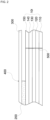
FIG. 2 is a sectional view taken along the line A-A' of the marking tag according to the present invention. -
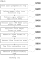
FIG. 3 is a flowchart showing a method for manufacturing the marking tag according to the present invention. -
100: Release paper 110: Base paper 120: Release paper color layer 130: Release paper adhesive layer 140: Release paper PET film layer 150: Silicone resin layer 200: Adhesive layer 300: Tag film 400: Adhesive guideline 500: Exhaust line - Hereinafter, an embodiment of the present invention will be described with reference to the accompanying drawings.
-
FIG. 1 shows top and underside of a marking tag according to the present invention, andFIG. 2 is a sectional view taken along the line A-A' of the marking tag according to the present invention. - A left figure of
FIG. 1 shows top of a marking tag according to the present invention, and a right figure thereof shows underside of the marking tag. - The marking tag according to the present invention largely includes a
release paper 100, anadhesive layer 200, and atag film 300. The solid lines ofFIGs. 1 and2 represent the parts seen from the outside, and the dotted lines thereof represent the parts existing on the underside of the marking tag according to the present invention. - The base paper constituting the
release paper 100 is a coated one side paper that has a minimal thickness and a size of 60/m2, is a white color, and is glossy on one side thereof, so that the release paper is minimized in thickness, while having its original function. This is to prevent the release paper itself from being thick excessively when a releasepaper color layer 120 formed by coating a red or yellow color onto top of the base paper to optimize the color contrasted with thetag film 300, a release paperPET film layer 140 formed by attaching a transparent release paper PET film on top of the releasepaper color layer 120 using an acrylic permanent adhesive to fix the releasepaper color layer 120 thereto, and asilicone resin layer 150 are laminated on top of one another to form therelease paper 100. In this case, desirably, the releasepaper color layer 120 has a thickness of 10 to 15 µm, and the release paperPET film layer 140 has a thickness of 16 to 19 µm. If a thick release paper is laminated on top of thetag film 300, the laminated material may not be wound in large amounts, and accordingly, the release paper has to be thin in thickness in such a way as to allow a sensor to obviously identify the release paper from thetag film 300. Thesilicone resin layer 150 is formed by applying a silicone resin onto top of the release paperPET film layer 140, thereby allowing therelease paper 100 to have its release function. - The
adhesive layer 200 is formed by applying an acrylic adhesive onto a portion of top of thesilicone resin layer 150 of therelease paper 100 and desirably has a thickness of 5 to 30 µm. According to the present invention, an acrylic removable adhesive is adopted to form theadhesive layer 200. Theadhesive layer 200 is attachedly coupled to one side of the underside of thetag film 300 corresponding to about 25 to 30% of the entire area of thetag film 300, which is shown inFIG. 1 . In this case, desirably, a PET film, which becomes thin to the thickness of 25 to 30 µm, is adopted as thetag film 300, and according to the present invention, the PET film with a white color is used as thetag film 300. - Further, at least one or more
adhesive guidelines 400 are desirably marked with solid lines or broken lines on a portion of top of thetag film 300 where theadhesive layer 200 is formed on the underside of thetag film 300 or around the portion so as to notify the user of a given attachment margin needed when the marking tag is attached onto the electrode or help appropriate tagging. InFIGs. 1 and2 , oneadhesive guideline 400 is marked with the solid line along a boundary line between theadhesive layer 200 and thetag film 300. Even though in specific not shown, in this case, two or moreadhesive guidelines 400 may be marked for the conveniences of the user. - Moreover, an
exhaust line 500 is additionally marked with a solid line or broken line by incising a portion where theadhesive layer 200 does not exist on therelease paper 100 along a longitudinal direction of therelease paper 100. Through theexhaust line 500, air existing in the space between thetag film 300 and therelease paper 100 in a state where thetag film 300 is laminated on top of therelease paper 100 is exhausted to the outside of therelease paper 100, thereby preventing the marking tag from being irregularly wound when the marking tag is wound, keeping thetag film 300 from getting loose, and suppressing the thickness of the marking tag wound from increasing. -
FIG. 3 is a flowchart showing a method for manufacturing the marking tag according to the present invention. - A base paper preparation step S100 is a step in which a base paper for a release paper is prepared. According to the present invention, desirably, the base paper is a coated one side paper that has a minimal thickness and a size of 60/m2, is a white color, and is glossy on one side thereof.
- A release paper color layer formation step S200 is a step in which a given color is coated onto the underside of the base paper and dried to form a release paper color layer. A red or yellow color is adopted as a color of the release paper color layer.
- A release paper adhesive application step S300 is a step in which a transparent acrylic permanent adhesive is applied onto top of the release paper color layer to form a release paper adhesive layer. To allow the release paper color layer to have its original function as the release paper, without any separation or peeling, the release paper adhesive layer is provided, and as the release paper adhesive layer is formed, further, the release paper PET film layer as will be discussed later is attached well thereto so that when a silicone resin is coated, a silicone resin layer as will be discussed later is formed well.
- After the release paper adhesive has been applied, a release paper PET film layer formation step S400 is carried out to attach the release paper PET film to top of the release paper adhesive layer.
- After that, a silicone resin layer formation step S500 is carried out to coat the silicone resin serving to perform release onto top of the release paper PET film, dry the coated silicone resin, and thus form the silicone resin layer.
- Through the above-mentioned steps, the release paper having the given color as one of the parts of the present invention is manufactured.
- After the release paper has been manufactured, further, an adhesive layer formation step S600 is carried out to apply an acrylic removable adhesive onto a portion of top of the silicone resin layer and thus form an adhesive layer having a thickness of 5 to 30 µm.
- After the adhesive layer formation step S600, if necessary, an exhaust line formation step S700 is carried out to form an exhaust line marked with a solid line or broken line by incising a portion where the adhesive layer does not exist on the release paper along a longitudinal direction of the release paper.
- After that, a tag film lamination step S800 is carried out to attach a tag film made of a synthetic resin and having a different color contrasted with the color of the release paper color layer to the adhesive layer, while one side of the underside of the tag film corresponding to about 25 to 30% of the entire area of the tag film is attached to the adhesive layer, and to laminate the tag film on top of the release paper, thereby manufacturing the marking tag according to the present invention.
- After the tag film lamination step S800, further, an adhesive guideline marking step S900 is carried out to form an adhesive guideline marked with a solid line or broken line on a portion of top of the tag film where the adhesive layer is formed on the underside of the tag film, so that the boundary of the portion is identified by the user to improve the conveniences of the user.
Claims (10)
- A tag for marking a defective portion of an electrode for a secondary battery, the tag comprising:a release paper having a base paper, a release paper color layer formed by coating a given color onto top of the base paper, a release paper adhesive layer formed by applying a transparent adhesive onto top of the release paper color layer, a release paper polyethylene terephthalate (PET) film layer formed by attaching a transparent release paper PET film onto top of the release paper color layer, and a silicone resin layer formed by applying a silicone resin onto top of the release paper PET film layer in such a way as to be laminated on top of one another sequentially;an adhesive layer formed by applying an acrylic adhesive onto a portion of top of the silicone resin layer of the release paper to a thickness of 5 to 30 µm; anda tag film integrally coupled to the adhesive layer in such a way as to attach the underside of one side corresponding to 25 to 50% of the entire area thereof onto the release paper, the tag film being made of a synthetic resin film with a different color contrasted with the given color of the release paper color layer.
- The tag according to claim 1, wherein the tag film is made of polyethylene terephthalate (PET).
- The tag according to claim 1, wherein the release paper color layer is a red or yellow color, and the tag film is a white color.
- The tag according to claim 1, wherein the release paper adhesive layer is made of an acrylic permanent adhesive.
- The tag according to claim 1, wherein the release paper adhesive layer has a thickness of 10 to 15 µm, the release paper PET film layer has a thickness of 16 to 25 µm, and the tag film has a thickness of 25 to 50 µm.
- The tag according to claim 1, further comprising one or more adhesive guidelines marked with solid lines or broken line on top of the tag film to identify the boundary of a portion where the adhesive layer is formed on the underside of the tag film.
- The tag according to any one of claims 1 to 6, further comprising an exhaust line marked with a solid line or broken line by incising a portion where the adhesive layer does not exist on the release paper along a longitudinal direction of the release paper.
- A method for manufacturing a tag for marking a defective portion of an electrode for a secondary battery, the method comprising the steps of:preparing a base paper used for a release paper;coating a given color onto top of the base paper and drying the coated color to form a release paper color layer;applying a transparent acrylic permanent adhesive onto top of the release paper color layer to form a release paper adhesive layer;attaching a transparent PET film onto top of the release paper color layer to form a release paper PET film layer;coating a silicone resin having a release function onto top of the release paper PET film layer and drying the coated silicone resin to form a silicone resin layer;applying an acrylic adhesive onto a portion of top of the silicone resin layer of the release paper to form an adhesive layer having a thickness of 5 to 30 µm; andcoupling a tag film made of a synthetic resin film with a different color contrasted with the given color of the release paper color layer to the adhesive layer in such a way as to attach the underside of one side corresponding to 25 to 50% of the entire area thereof to the adhesive layer and thus laminating the tag film on top of the release paper.
- The method according to claim 8, after the step of forming the adhesive layer, further comprising the step of forming an exhaust line marked with a solid line or broken line by incising a portion where the adhesive layer does not exist on the release paper along a longitudinal direction of the release paper.
- The method according to claim 8 or 9, after the step of laminating the tag film to the release paper, further comprising the step of forming one or more adhesive guidelines marked with solid lines or broken line on top of the tag film to identify the boundary of a portion where the adhesive layer is formed on the underside of the tag film.
Applications Claiming Priority (2)
| Application Number | Priority Date | Filing Date | Title |
|---|---|---|---|
| KR1020210023655A KR102400736B1 (en) | 2021-02-22 | 2021-02-22 | Tag for marking defective parts of secondary battery electrode and manufacturing process thereof |
| PCT/KR2022/000155 WO2022177148A1 (en) | 2021-02-22 | 2022-01-05 | Tag for marking defective portions of electrode for secondary battery and method for manufacturing same |
Publications (2)
| Publication Number | Publication Date |
|---|---|
| EP4296997A1 true EP4296997A1 (en) | 2023-12-27 |
| EP4296997A4 EP4296997A4 (en) | 2025-03-12 |
Family
ID=81804028
Family Applications (1)
| Application Number | Title | Priority Date | Filing Date |
|---|---|---|---|
| EP22756355.8A Pending EP4296997A4 (en) | 2021-02-22 | 2022-01-05 | Tag for marking defective portions of electrode for secondary battery and method for manufacturing same |
Country Status (6)
| Country | Link |
|---|---|
| US (1) | US12548476B2 (en) |
| EP (1) | EP4296997A4 (en) |
| KR (1) | KR102400736B1 (en) |
| CN (1) | CN116802712B (en) |
| CA (1) | CA3206420A1 (en) |
| WO (1) | WO2022177148A1 (en) |
Family Cites Families (24)
| Publication number | Priority date | Publication date | Assignee | Title |
|---|---|---|---|---|
| US6210524B1 (en) * | 1999-09-03 | 2001-04-03 | Avery Dennison Corporation | Method of improving peel-plate dispensability of label constructions |
| US6497933B1 (en) * | 2000-04-21 | 2002-12-24 | The Standard Register Company | Antistatic composition for use in a label construction |
| JP2005122068A (en) * | 2003-10-20 | 2005-05-12 | Dainippon Printing Co Ltd | Adhesive label for opening identification |
| CN101049743A (en) * | 2007-04-20 | 2007-10-10 | 上海紫泉标签有限公司 | Label inside composite membrane |
| ES2383095T3 (en) * | 2007-09-06 | 2012-06-18 | Upm Raflatac Oy | A method of manufacturing a label laminate |
| BRPI0916023A2 (en) * | 2008-11-13 | 2015-11-10 | 3M Innovative Properties Co | "tag stack and method for tagging an article" |
| KR200455593Y1 (en) * | 2011-02-22 | 2011-09-15 | 주식회사 부영월드 | Label |
| KR20120102328A (en) * | 2011-03-08 | 2012-09-18 | 조은미 | Removable labels for identification of bad rechargeable batteries |
| US20120263905A1 (en) * | 2011-04-13 | 2012-10-18 | Park Mi-Suk | Adhesive sticker and manufacturing method thereof |
| KR101330880B1 (en) | 2011-11-03 | 2013-11-18 | 조은미 | Removable label for identifying bad electlode of secondary cell |
| KR20130085141A (en) * | 2012-01-19 | 2013-07-29 | 전영준 | Offset printing ink material and method for manufacturing the label using thereof and label |
| EP2851194B1 (en) * | 2013-09-20 | 2015-12-16 | Hueck Folien Ges.m.b.H | Safety element, in particular safety label |
| CN203982692U (en) * | 2014-07-21 | 2014-12-03 | 上海中商网络股份有限公司 | Wet sensitive information anti-fake labeling |
| CN204537622U (en) * | 2015-03-27 | 2015-08-05 | 福建联迪商用设备有限公司 | A kind of novel VOID antifalsification label structure |
| JP2016191843A (en) * | 2015-03-31 | 2016-11-10 | サトーホールディングス株式会社 | Label roll, label roll manufacturing method, label roll use method |
| US10532533B2 (en) * | 2015-06-05 | 2020-01-14 | Upm Raflatac Oy | Adhesive label, facestock for an adhesive label and adhesive label laminate |
| US20170337851A1 (en) * | 2016-05-18 | 2017-11-23 | Clearvue, Llc | Reveal substrates and method of forming same |
| KR102165099B1 (en) * | 2017-06-01 | 2020-10-13 | 주식회사 엘지화학 | Multilayer marking film |
| JP7156874B2 (en) * | 2018-09-07 | 2022-10-19 | リンテック株式会社 | LASER MARKER LABEL AND LASER MARKER LABEL MANUFACTURING METHOD |
| KR102100636B1 (en) * | 2019-07-10 | 2020-04-21 | 주식회사 무궁화엘앤비 | Void rabel with security element and manufacturing method thereof |
| EP4110705A1 (en) * | 2020-02-26 | 2023-01-04 | Avery Dennison Retail Information Services LLC | Rfid security label for packaging |
| CN210984037U (en) * | 2020-03-25 | 2020-07-10 | 何玉珠 | Environment-friendly adhesive label |
| KR102413265B1 (en) * | 2021-01-14 | 2022-06-24 | 조은미 | Detecting label for defect of electrode for secondary battery and manufacturing process thereof |
| FI131745B1 (en) * | 2023-11-03 | 2025-11-03 | Upm Raflatac Oy | Linerless wash-off label |
-
2021
- 2021-02-22 KR KR1020210023655A patent/KR102400736B1/en active Active
-
2022
- 2022-01-05 WO PCT/KR2022/000155 patent/WO2022177148A1/en not_active Ceased
- 2022-01-05 CA CA3206420A patent/CA3206420A1/en active Pending
- 2022-01-05 US US18/271,863 patent/US12548476B2/en active Active
- 2022-01-05 EP EP22756355.8A patent/EP4296997A4/en active Pending
- 2022-01-05 CN CN202280010225.8A patent/CN116802712B/en active Active
Also Published As
| Publication number | Publication date |
|---|---|
| US12548476B2 (en) | 2026-02-10 |
| KR102400736B1 (en) | 2022-05-23 |
| WO2022177148A1 (en) | 2022-08-25 |
| CN116802712B (en) | 2026-04-07 |
| US20240304115A1 (en) | 2024-09-12 |
| CN116802712A (en) | 2023-09-22 |
| CA3206420A1 (en) | 2022-08-25 |
| EP4296997A4 (en) | 2025-03-12 |
Similar Documents
| Publication | Publication Date | Title |
|---|---|---|
| US6210767B1 (en) | Release liner base stock for printed films or labels | |
| EP4276803A1 (en) | Both side-recognizable label for identifying defective portion of electrode for secondary battery and manufacturing method therefor | |
| US5691022A (en) | Release liner base stock for printed films or labels | |
| KR100406015B1 (en) | Single ply psa labels for battery applications | |
| EP0819298B1 (en) | Strip coated adhesive products | |
| US20020084026A1 (en) | Multiple layer labels and methods | |
| US10072190B2 (en) | Digital printed duct tape | |
| KR101330880B1 (en) | Removable label for identifying bad electlode of secondary cell | |
| US12548476B2 (en) | Tag for marking defective part of electrode for secondary battery and manufacturing method thereof | |
| WO2004072930A1 (en) | Shrinkable battery label | |
| TW201103105A (en) | Die adhesive film, reel for die adhesive film, and mounting apparatus comprising the same | |
| KR20120068815A (en) | A method of producing thin batteries | |
| CN210236602U (en) | Line mechanism is peeled off to gravure coated paper | |
| CN220672123U (en) | Waterproof scratch-resistant corrosion-resistant label | |
| CN115513504B (en) | Fuel cell membrane electrode GDL laminating device and method | |
| JP4707901B2 (en) | Forensic adhesive sheet | |
| AU681775B2 (en) | Self-contained transfer tape | |
| CN111287019A (en) | Preparation method of laser anti-counterfeiting moisturizing and moisturizing composite packaging material | |
| KR20120102328A (en) | Removable labels for identification of bad rechargeable batteries | |
| JP2000301546A (en) | Liner for winding long raw rubber members | |
| US10603881B2 (en) | Digital printed duct tape | |
| CN110352227B (en) | Digital printing pipeline adhesive tape | |
| WO2016085055A1 (en) | Method for manufacturing protective sheet for touch screen panel by using jig, and protective sheet manufactured thereby | |
| CN217578761U (en) | Anti-counterfeiting protective film | |
| CN208970019U (en) | A kind of label adhesive paper |
Legal Events
| Date | Code | Title | Description |
|---|---|---|---|
| STAA | Information on the status of an ep patent application or granted ep patent |
Free format text: STATUS: THE INTERNATIONAL PUBLICATION HAS BEEN MADE |
|
| PUAI | Public reference made under article 153(3) epc to a published international application that has entered the european phase |
Free format text: ORIGINAL CODE: 0009012 |
|
| STAA | Information on the status of an ep patent application or granted ep patent |
Free format text: STATUS: REQUEST FOR EXAMINATION WAS MADE |
|
| 17P | Request for examination filed |
Effective date: 20230920 |
|
| AK | Designated contracting states |
Kind code of ref document: A1 Designated state(s): AL AT BE BG CH CY CZ DE DK EE ES FI FR GB GR HR HU IE IS IT LI LT LU LV MC MK MT NL NO PL PT RO RS SE SI SK SM TR |
|
| DAV | Request for validation of the european patent (deleted) | ||
| DAX | Request for extension of the european patent (deleted) | ||
| A4 | Supplementary search report drawn up and despatched |
Effective date: 20250207 |
|
| RIC1 | Information provided on ipc code assigned before grant |
Ipc: C09J 7/38 20180101ALI20250203BHEP Ipc: C09J 7/40 20180101ALI20250203BHEP Ipc: C09J 133/04 20060101ALI20250203BHEP Ipc: B32B 7/12 20060101ALI20250203BHEP Ipc: B32B 7/06 20190101ALI20250203BHEP Ipc: B32B 27/36 20060101ALI20250203BHEP Ipc: B32B 27/10 20060101ALI20250203BHEP Ipc: B32B 27/08 20060101ALI20250203BHEP Ipc: B32B 3/30 20060101ALI20250203BHEP Ipc: H01M 10/04 20060101ALI20250203BHEP Ipc: H01M 4/04 20060101ALI20250203BHEP Ipc: G09F 3/02 20060101AFI20250203BHEP |