EP4296770A1 - Optical computation device and optical computation method - Google Patents
Optical computation device and optical computation method Download PDFInfo
- Publication number
- EP4296770A1 EP4296770A1 EP22755784.0A EP22755784A EP4296770A1 EP 4296770 A1 EP4296770 A1 EP 4296770A1 EP 22755784 A EP22755784 A EP 22755784A EP 4296770 A1 EP4296770 A1 EP 4296770A1
- Authority
- EP
- European Patent Office
- Prior art keywords
- light
- diffraction element
- optical computing
- computing device
- light diffraction
- Prior art date
- Legal status (The legal status is an assumption and is not a legal conclusion. Google has not performed a legal analysis and makes no representation as to the accuracy of the status listed.)
- Pending
Links
Images

Classifications
-
- G—PHYSICS
- G02—OPTICS
- G02B—OPTICAL ELEMENTS, SYSTEMS OR APPARATUS
- G02B27/00—Optical systems or apparatus not provided for by any of the groups G02B1/00 - G02B26/00, G02B30/00
- G02B27/42—Diffraction optics, i.e. systems including a diffractive element being designed for providing a diffractive effect
- G02B27/4233—Diffraction optics, i.e. systems including a diffractive element being designed for providing a diffractive effect having a diffractive element [DOE] contributing to a non-imaging application
- G02B27/4244—Diffraction optics, i.e. systems including a diffractive element being designed for providing a diffractive effect having a diffractive element [DOE] contributing to a non-imaging application in wavelength selecting devices
-
- G—PHYSICS
- G06—COMPUTING OR CALCULATING; COUNTING
- G06E—OPTICAL COMPUTING DEVICES
- G06E3/00—Devices not provided for in group G06E1/00, e.g. for processing analogue or hybrid data
- G06E3/001—Analogue devices in which mathematical operations are carried out with the aid of optical or electro-optical elements
-
- G—PHYSICS
- G02—OPTICS
- G02B—OPTICAL ELEMENTS, SYSTEMS OR APPARATUS
- G02B27/00—Optical systems or apparatus not provided for by any of the groups G02B1/00 - G02B26/00, G02B30/00
- G02B27/42—Diffraction optics, i.e. systems including a diffractive element being designed for providing a diffractive effect
- G02B27/4294—Diffraction optics, i.e. systems including a diffractive element being designed for providing a diffractive effect in multispectral systems, e.g. UV and visible
-
- G—PHYSICS
- G02—OPTICS
- G02B—OPTICAL ELEMENTS, SYSTEMS OR APPARATUS
- G02B5/00—Optical elements other than lenses
- G02B5/18—Diffraction gratings
- G02B5/1814—Diffraction gratings structurally combined with one or more further optical elements, e.g. lenses, mirrors, prisms or other diffraction gratings
- G02B5/1819—Plural gratings positioned on the same surface, e.g. array of gratings
-
- G—PHYSICS
- G02—OPTICS
- G02B—OPTICAL ELEMENTS, SYSTEMS OR APPARATUS
- G02B5/00—Optical elements other than lenses
- G02B5/18—Diffraction gratings
- G02B5/1842—Gratings for image generation
-
- G—PHYSICS
- G02—OPTICS
- G02B—OPTICAL ELEMENTS, SYSTEMS OR APPARATUS
- G02B5/00—Optical elements other than lenses
- G02B5/18—Diffraction gratings
- G02B5/1866—Transmission gratings characterised by their structure, e.g. step profile, contours of substrate or grooves, pitch variations, materials
-
- G—PHYSICS
- G02—OPTICS
- G02B—OPTICAL ELEMENTS, SYSTEMS OR APPARATUS
- G02B5/00—Optical elements other than lenses
- G02B5/18—Diffraction gratings
- G02B2005/1804—Transmission gratings
-
- G—PHYSICS
- G06—COMPUTING OR CALCULATING; COUNTING
- G06N—COMPUTING ARRANGEMENTS BASED ON SPECIFIC COMPUTATIONAL MODELS
- G06N3/00—Computing arrangements based on biological models
- G06N3/02—Neural networks
- G06N3/06—Physical realisation, i.e. hardware implementation of neural networks, neurons or parts of neurons
- G06N3/067—Physical realisation, i.e. hardware implementation of neural networks, neurons or parts of neurons using optical means
Definitions
- the present invention relates to an optical computing device and an optical computing method each of which performs optical computing with use of a light diffraction element.
- a light diffraction element which includes a plurality of microcells and which is designed to optically carry out predetermined computing by causing signal light beams that have passed through the microcells to mutually interfere with each other.
- Optical computing carried out with use of a light diffraction element has an advantage of achieving higher speed and lower electric power consumption as compared with electrical computing carried out with use of a processor.
- Patent Literature 1 discloses an optical neural network having an input layer, an intermediate layer, and an output layer. The optical filter described above can be used as, for example, an intermediate layer of such an optical neural network.
- Patent Literature 1 Specification of US Patent No. 7847225
- Such a conventional optical computing device have been designed such that, when signal light having a specific wavelength is inputted into a light diffraction element of the optical computing device, the light diffraction element performs desired optical computing.
- the light diffraction element performs desired optical computing.
- a plurality of wavelength components (discrete spectrum) or countless wavelength components (continuous spectrum) contained in signal light only a wavelength component having a specific wavelength is used for optical computing, and other wavelength components are wasted, without being used for the optical computing.
- An aspect of the present invention has been achieved in light of the foregoing problem. It is an object of the aspect of the present invention to achieve an optical computing device and an optical computing method each of which can use, for optical computing, a plurality of wavelength components contained in signal light.
- An optical computing device in accordance with an aspect of the present invention includes: a light diffraction element group including at least one light diffraction element having an optical computing function; and a light receiving section configured to individually detect respective intensities of a plurality of wavelength components contained in signal light outputted from the light diffraction element group.
- An optical computing method is an optical computing method that uses a light diffraction element group including at least one light diffraction element having an optical computing function, the method including the step of: individually detecting respective intensities of a plurality of wavelength components contained in signal light outputted from the light diffraction element group.
- optical computing device or optical computing method each of which can use, for optical computing, a plurality of wavelength components contained in signal light.
- FIG. 1 is a perspective view illustrating a configuration of the optical computing device 1.
- the optical computing device 1 includes a light emitting section 11, a light diffraction element group 12, and a light receiving section 13.
- the light emitting section 11 is configured to generate signal light that is polychromatic light.
- the term “signal light” refers to light having a two-dimensional intensity distribution depending on a signal.
- the expression “signal light that is polychromatic light” refers to signal light which contains a plurality of wavelength components.
- used as the light emitting section 11 is a display configured to generate signal light containing a plurality of wavelength components belonging to a visible light band.
- used as the light emitting section 11 is a display configured to generate signal light containing a blue component, a green component, and a red component.
- the signal light outputted from the light emitting section 11 is also referred to as "input signal light”.
- the light diffraction element group 12 is arranged on a light path of the input signal light.
- the light diffraction element group 12 is a set of n light diffraction elements 12a1 to 12an.
- n is a natural number that is not less than 1.
- Each light diffraction element 12ai is configured to perform predetermined optical computing.
- each light diffraction element 12ai is configured to convert a two-dimensional intensity distribution of signal light in accordance with a predetermined conversion rule.
- i is a natural number that is not less than 1 and not more than n.
- a set of two light diffraction elements 12a1 and 12a2 is used as the light diffraction element group 12.
- the configuration of the light diffraction element 12ai will be described later with reference to another drawing.
- the light diffraction elements 12a1 to 12an are arranged side by side in a straight line on the light path of the input signal light.
- the input signal light passes through a first light diffraction element 12a1, a second light diffraction element 12a2, ... , and an n-th light diffraction element 12an in this order. Therefore, in the light diffraction element group 12, the input signal light is subjected to first optical computing performed by the first light diffraction element 12a1, second optical computing performed by the second light diffraction element 12a2, and n-th optical computing performed by the n-th light diffraction element 12an, in this order.
- the intensity distribution of the signal light outputted from the light diffraction element group 12 shows computation results of these computing processes.
- the signal light outputted from the light diffraction element group 12 is also referred to as "output signal light”.
- the light receiving section 13 is arranged on a light path of the output signal light.
- the light receiving section 13 is configured to individually detect respective two-dimensional intensity distributions of a plurality of wavelength components contained in output signal light.
- a multispectral camera which individually detects respective two-dimensional intensity distributions of a plurality of wavelength components belonging to a visible light band.
- a multispectral camera configured to individually detect respective two-dimensional intensity distributions of blue, green, and red components. Note that the multispectral camera refers to a camera that is capable of individually detecting two-dimensional intensity distributions in ten or more wavelength bands.
- a hyperspectral camera may be used as the light receiving section 13.
- the hyperspectral camera refers to a camera that can individually detect two-dimensional intensity distributions in 100 or more wavelength bands.
- the wavelength components contained in input signal light may (1) have the same two-dimensional intensity distribution, that is, indicate the same signal or (2) have different two-dimensional intensity distributions, that is, indicate different signals.
- the optical computing device 1 can provide m computation results f1(x), f2(x), ... , and fm(x) with respect to the input signal x.
- m classification results f1(x), f2(x), ... , fm(x) it is possible to provide, as classification results of a subject contained in the input images x, m classification results f1(x), f2(x), ... , fm(x).
- the optical computing device 1 can provide a more accurate or more detailed computation result than that provided through single-wavelength optical computing.
- a more accurate computation result f(x) for example, an average of the m computation results f1(x), f2(x), ... , and fm(x) may be calculated.
- a more detailed computation result f(x) for example, a direct product of the m computation results f1(x), f2(x), ... , and fm(x) need only be calculated.
- the optical computing device 1 can provide computation results f1(x1), f2(x2), ... , and fn(xn) with respect to the respective m input signals x1, x2, ... , and xm.
- the two-dimensional intensity distributions of the m wavelength components contained in the input signal light indicate different input images x1, x2, ... , and xm
- the optical computing device 1 can provide a greater variety of computation results than the ones provided through the single-wavelength optical computing.
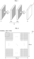
- Fig. 2 is a plan view illustrating a configuration of the light diffraction element 12ai.
- Fig. 3 is a perspective view illustrating an enlarged part (part enclosed by a dotted line in Fig. 2 ) of the light diffraction element 12ai.
- the light diffraction element 12ai is constituted by a plurality of microcells having respective thicknesses or refractive indices that are set independently of each other.
- signal light enters the light diffraction element 12ai, signal light beams that have been diffracted in the respective microcells and that have different phases interfere with each other, so that predetermined optical computing (conversion of a two-dimensional intensity distribution in accordance with a predetermined conversion rule) is performed.
- the term "microcell” refers to, for example, a cell having a cell size of less than 10 pm.
- the term "cell size" refers to a square root of an area of a cell. For example, in a case where a microcell has a square shape in plan view, the cell size is a length of one side of the cell. The cell size has a lower limit that is, for example, 1 nm.
- the light diffraction element 12ai illustrated in Fig. 2 is constituted by 200 ⁇ 200 microcells arranged in a matrix pattern. Each of the microcells has a square shape having a size of 500 nm ⁇ 500 nm in plan view, and the light diffraction element 12ai has a square shape having a size of 100 pm ⁇ 100 pm in plan view.
- a phase-shift amount of light that passes through a microcell can be set independently for each of the cells by (1) setting a thickness of the microcell independently for each of the cells or (2) setting a refractive index of the microcell independently for each of the cells.
- the present embodiment employs the method (1), which can be performed through nanoimprinting.
- each of the microcells is constituted by a pillar that has a quadrangular prism shape and that has a square bottom surface which has sides each having a length equal to a cell size.
- a phase-shift amount of light that passes through a microcell is determined in accordance with a height of the pillar. That is, the light that passes through the microcell which is constituted by a high pillar has a large phase-shift amount, and the light that passes through the microcell which is constituted by a low pillar has a small phase-shift amount.
- the thickness or refractive index of each of the microcells can be set, for example, through machine learning.
- a model used in this machine learning can be, for example, a model in which a two-dimensional intensity distribution of signal light inputted into the light diffraction element 12ai is an input, and a two-dimensional intensity distribution of signal light outputted from the light diffraction element 12ai is an output and which includes a thickness or refractive index of each of the microcells as a parameter.
- the two-dimensional intensity distribution of the signal light inputted into the light diffraction element 12ai means a set of intensities of signal light beams inputted into the respective microcells that constitute the light diffraction element 12ai.
- the two-dimensional intensity distribution of the signal light outputted from the light diffraction element 12ai means: a set of intensities of signal light beams inputted into respective microcells that constitute a light diffraction element 12ai+1 arranged so as to follow the light diffraction element 12ai; or a set of intensities of signal light beams inputted into respective microcells that constitute the light receiving section 13 arranged so as to follow the light diffraction element 12ai.
- FIG. 4 is a perspective view illustrating a configuration of the optical computing device 1A.
- the optical computing device 1A includes a light emitting section 11, a light diffraction element group 12, and a light receiving section 13A.
- the light emitting section 11 and the light diffraction element group 12 which are included in the optical computing device 1A illustrated in Fig. 4 are configured respectively in the same manner as the light emitting section 11 and the light diffraction element group 12 which are included in the optical computing device 1 illustrated in Fig. 1 .
- the light receiving section 13 included in the optical computing device 1 illustrated in Fig. 1 is configured to individually detect respective two-dimensional intensity distributions of wavelength components contained in output signal light
- the light receiving section 13A included in the optical computing device 1A illustrated in Fig. 4 is configured to individually detect respective intensities of wavelength components contained in output signal light at a specific point.
- a computation result can be provided, for example, by specifying which wavelength component the light receiving section 13 has detected, among wavelength components contained in output signal light.
- each light diffraction element 12ai included in the light diffraction element group 12 need only be designed such that a wavelength component which corresponds to a computation result enters the light receiving section 13A, while a wavelength component which does not correspond to the computation result does not enter the light receiving section 13A.
- a computing section configured to specify, on the basis of the output signal from the light receiving section 13, which wavelength component the light receiving section 13 has detected, among wavelength components contained in output signal light need only be added to constituent elements of the optical computing device 1.
- An optical computing device includes: a light diffraction element group including at least one light diffraction element having an optical computing function; and a light receiving section configured to individually detect respective intensities of a plurality of wavelength components contained in signal light outputted from the light diffraction element group.
- optical computing device which can use, for optical computing, a plurality of wavelength components contained in signal light.
- An optical computing device employs, in addition to the configuration of Aspect 1, a configuration such that the light receiving section is configured to individually detect respective two-dimensional intensity distributions of the plurality of wavelength components contained in the signal light outputted from the light diffraction element group.
- An optical computing device employs, in addition to the configuration of Aspect 2, a configuration such that the optical computing device further includes a light emitting section configured to generate signal light that is to be inputted into the light diffraction element group and that contains a plurality of wavelength components having the same two-dimensional intensity distribution.
- An optical computing device employs, in addition to the configuration of Aspect 2, a configuration such that the optical computing device further includes a light emitting section configured to generate signal light that is to be inputted into the light diffraction element and that contains a plurality of wavelength components having different two-dimensional intensity distributions.
- An optical computing device employs, in addition to the configuration of any one of Aspects 2 to 4, a configuration such that the light receiving section is a multispectral camera.
- An optical computing device employs, in addition to the configuration of Aspect 1, a configuration such that the light receiving section is configured to individually detect, at a specific point, respective intensities of a plurality of wavelength components contained in signal light outputted from the light diffraction element group.
- An optical computing device employs, in addition to the configuration of Aspect 6, a configuration such that the optical computing device further includes a computing section configured to specify, on a basis of an output signal from the light receiving section, which wavelength component the light receiving section has detected, among wavelength components contained in the signal light outputted from the light diffraction element group.
- An optical computing device employs, in addition to the configuration of any one of Aspects 1 to 7, a configuration such that the light diffraction element is constituted by a plurality of microcells having respective thicknesses or refractive indices that are set independently of each other.
- An optical computing method is an optical computing method that uses a light diffraction element group including at least one light diffraction element having an optical computing function, the method including the step of: individually detecting respective intensities of a plurality of wavelength components contained in signal light outputted from the light diffraction element group.
Landscapes
- Physics & Mathematics (AREA)
- Optics & Photonics (AREA)
- General Physics & Mathematics (AREA)
- Spectroscopy & Molecular Physics (AREA)
- Engineering & Computer Science (AREA)
- Theoretical Computer Science (AREA)
- Mathematical Physics (AREA)
- Nonlinear Science (AREA)
- Optical Modulation, Optical Deflection, Nonlinear Optics, Optical Demodulation, Optical Logic Elements (AREA)
- Spectrometry And Color Measurement (AREA)
- Diffracting Gratings Or Hologram Optical Elements (AREA)
- Photometry And Measurement Of Optical Pulse Characteristics (AREA)
Abstract
Description
- The present invention relates to an optical computing device and an optical computing method each of which performs optical computing with use of a light diffraction element.
- A light diffraction element has been known which includes a plurality of microcells and which is designed to optically carry out predetermined computing by causing signal light beams that have passed through the microcells to mutually interfere with each other. Optical computing carried out with use of a light diffraction element has an advantage of achieving higher speed and lower electric power consumption as compared with electrical computing carried out with use of a processor.
Patent Literature 1 discloses an optical neural network having an input layer, an intermediate layer, and an output layer. The optical filter described above can be used as, for example, an intermediate layer of such an optical neural network. - [Patent Literature 1]
Specification ofUS Patent No. 7847225 - Such a conventional optical computing device have been designed such that, when signal light having a specific wavelength is inputted into a light diffraction element of the optical computing device, the light diffraction element performs desired optical computing. Among a plurality of wavelength components (discrete spectrum) or countless wavelength components (continuous spectrum) contained in signal light, only a wavelength component having a specific wavelength is used for optical computing, and other wavelength components are wasted, without being used for the optical computing.
- An aspect of the present invention has been achieved in light of the foregoing problem. It is an object of the aspect of the present invention to achieve an optical computing device and an optical computing method each of which can use, for optical computing, a plurality of wavelength components contained in signal light.
- An optical computing device in accordance with an aspect of the present invention includes: a light diffraction element group including at least one light diffraction element having an optical computing function; and a light receiving section configured to individually detect respective intensities of a plurality of wavelength components contained in signal light outputted from the light diffraction element group.
- An optical computing method according to an aspect of the present invention is an optical computing method that uses a light diffraction element group including at least one light diffraction element having an optical computing function, the method including the step of: individually detecting respective intensities of a plurality of wavelength components contained in signal light outputted from the light diffraction element group.
- According to an aspect of the present invention, it is possible to achieve an optical computing device or optical computing method each of which can use, for optical computing, a plurality of wavelength components contained in signal light.
-
-
Fig. 1 is a perspective view illustrating a configuration of an optical computing device in accordance with an embodiment of the present invention. -
Fig. 2 is a plan view illustrating a configuration of a light diffraction element included in the optical computing device illustrated inFig. 1 . -
Fig. 3 is a perspective view illustrating an enlarged part of the light diffraction element illustrated inFig. 2 . -
Fig. 4 is a perspective view illustrating a variation of the optical computing device illustrated inFig. 1 . - With reference to
Fig. 1 , the following will describe anoptical computing device 1 in accordance with an embodiment of the present invention.Fig. 1 is a perspective view illustrating a configuration of theoptical computing device 1. - As illustrated in
Fig. 1 , theoptical computing device 1 includes alight emitting section 11, a lightdiffraction element group 12, and alight receiving section 13. - The
light emitting section 11 is configured to generate signal light that is polychromatic light. Here, the term "signal light" refers to light having a two-dimensional intensity distribution depending on a signal. Further, the expression "signal light that is polychromatic light" refers to signal light which contains a plurality of wavelength components. In the present embodiment, used as thelight emitting section 11 is a display configured to generate signal light containing a plurality of wavelength components belonging to a visible light band. As one example, used as thelight emitting section 11 is a display configured to generate signal light containing a blue component, a green component, and a red component. Hereinafter, the signal light outputted from thelight emitting section 11 is also referred to as "input signal light". - The light
diffraction element group 12 is arranged on a light path of the input signal light. The lightdiffraction element group 12 is a set of n light diffraction elements 12a1 to 12an. Here, n is a natural number that is not less than 1. Each light diffraction element 12ai is configured to perform predetermined optical computing. In other words, each light diffraction element 12ai is configured to convert a two-dimensional intensity distribution of signal light in accordance with a predetermined conversion rule. Here, i is a natural number that is not less than 1 and not more than n. In the present embodiment, a set of two light diffraction elements 12a1 and 12a2 is used as the lightdiffraction element group 12. The configuration of the light diffraction element 12ai will be described later with reference to another drawing. - In the light
diffraction element group 12, the light diffraction elements 12a1 to 12an are arranged side by side in a straight line on the light path of the input signal light. Thus, the input signal light passes through a first light diffraction element 12a1, a second light diffraction element 12a2, ... , and an n-th light diffraction element 12an in this order. Therefore, in the lightdiffraction element group 12, the input signal light is subjected to first optical computing performed by the first light diffraction element 12a1, second optical computing performed by the second light diffraction element 12a2, and n-th optical computing performed by the n-th light diffraction element 12an, in this order. The intensity distribution of the signal light outputted from the lightdiffraction element group 12 shows computation results of these computing processes. Hereinafter, the signal light outputted from the lightdiffraction element group 12 is also referred to as "output signal light". - The
light receiving section 13 is arranged on a light path of the output signal light. Thelight receiving section 13 is configured to individually detect respective two-dimensional intensity distributions of a plurality of wavelength components contained in output signal light. In the present embodiment, used as thelight receiving section 13 is a multispectral camera which individually detects respective two-dimensional intensity distributions of a plurality of wavelength components belonging to a visible light band. As one example, used as thelight receiving section 13 is a multispectral camera configured to individually detect respective two-dimensional intensity distributions of blue, green, and red components. Note that the multispectral camera refers to a camera that is capable of individually detecting two-dimensional intensity distributions in ten or more wavelength bands. Further, in a case where wavelength components more than the wavelength components contained in the output signal light are required to be detected, a hyperspectral camera may be used as thelight receiving section 13. Here, the hyperspectral camera refers to a camera that can individually detect two-dimensional intensity distributions in 100 or more wavelength bands. - The wavelength components contained in input signal light may (1) have the same two-dimensional intensity distribution, that is, indicate the same signal or (2) have different two-dimensional intensity distributions, that is, indicate different signals.
- In a case where the input signal light and the output signal light each contain m wavelength components, and two-dimensional intensity distributions of the m wavelength components contained in the input signal light indicate the same input signal x, the
optical computing device 1 can provide m computation results f1(x), f2(x), ... , and fm(x) with respect to the input signal x. As one example, in a case where the two-dimensional intensity distributions of the m wavelength components contained in the input signal light indicate the same input image x, it is possible to provide, as classification results of a subject contained in the input images x, m classification results f1(x), f2(x), ... , fm(x). Thus, theoptical computing device 1 can provide a more accurate or more detailed computation result than that provided through single-wavelength optical computing. In a case where a more accurate computation result f(x) is required, for example, an average of the m computation results f1(x), f2(x), ... , and fm(x) may be calculated. Further, in a case where a more detailed computation result f(x) is required, for example, a direct product of the m computation results f1(x), f2(x), ... , and fm(x) need only be calculated. - In contrast, in a case where the input signal light and the output signal light each contain m wavelength components, and two-dimensional intensity distributions of the m wavelength components contained in the input signal light indicate different input signals x1, x2, ... , and xm, the
optical computing device 1 can provide computation results f1(x1), f2(x2), ... , and fn(xn) with respect to the respective m input signals x1, x2, ... , and xm. As one example, in a case where the two-dimensional intensity distributions of the m wavelength components contained in the input signal light indicate different input images x1, x2, ... , and xm, it is possible to provide, as classification results of subjects contained in the input images x1, x2, ... , xn, m classification results f1(x1), f2(x2), ... , and fm(xn). Thus, theoptical computing device 1 can provide a greater variety of computation results than the ones provided through the single-wavelength optical computing. - With reference to
Figs. 2 and3 , the following will describe a configuration of the light diffraction element 12ai.Fig. 2 is a plan view illustrating a configuration of the light diffraction element 12ai.Fig. 3 is a perspective view illustrating an enlarged part (part enclosed by a dotted line inFig. 2 ) of the light diffraction element 12ai. - The light diffraction element 12ai is constituted by a plurality of microcells having respective thicknesses or refractive indices that are set independently of each other. When signal light enters the light diffraction element 12ai, signal light beams that have been diffracted in the respective microcells and that have different phases interfere with each other, so that predetermined optical computing (conversion of a two-dimensional intensity distribution in accordance with a predetermined conversion rule) is performed. Note that, in the present specification, the term "microcell" refers to, for example, a cell having a cell size of less than 10 pm. Further, in the present specification, the term "cell size" refers to a square root of an area of a cell. For example, in a case where a microcell has a square shape in plan view, the cell size is a length of one side of the cell. The cell size has a lower limit that is, for example, 1 nm.
- The light diffraction element 12ai illustrated in
Fig. 2 is constituted by 200 × 200 microcells arranged in a matrix pattern. Each of the microcells has a square shape having a size of 500 nm × 500 nm in plan view, and the light diffraction element 12ai has a square shape having a size of 100 pm × 100 pm in plan view. - A phase-shift amount of light that passes through a microcell can be set independently for each of the cells by (1) setting a thickness of the microcell independently for each of the cells or (2) setting a refractive index of the microcell independently for each of the cells. The present embodiment employs the method (1), which can be performed through nanoimprinting. In this case, as illustrated in
Fig. 3 , each of the microcells is constituted by a pillar that has a quadrangular prism shape and that has a square bottom surface which has sides each having a length equal to a cell size. In this case, a phase-shift amount of light that passes through a microcell is determined in accordance with a height of the pillar. That is, the light that passes through the microcell which is constituted by a high pillar has a large phase-shift amount, and the light that passes through the microcell which is constituted by a low pillar has a small phase-shift amount. - Note that the thickness or refractive index of each of the microcells can be set, for example, through machine learning. A model used in this machine learning can be, for example, a model in which a two-dimensional intensity distribution of signal light inputted into the light diffraction element 12ai is an input, and a two-dimensional intensity distribution of signal light outputted from the light diffraction element 12ai is an output and which includes a thickness or refractive index of each of the microcells as a parameter. Here, the two-dimensional intensity distribution of the signal light inputted into the light diffraction element 12ai means a set of intensities of signal light beams inputted into the respective microcells that constitute the light diffraction element 12ai. Further, the two-dimensional intensity distribution of the signal light outputted from the light diffraction element 12ai means: a set of intensities of signal light beams inputted into respective microcells that constitute a light diffraction element 12ai+1 arranged so as to follow the light diffraction element 12ai; or a set of intensities of signal light beams inputted into respective microcells that constitute the
light receiving section 13 arranged so as to follow the light diffraction element 12ai. - With reference to
Fig. 4 , the following will describe a variation (hereinafter, referred to asoptical computing device 1A) of theoptical computing device 1.Fig. 4 is a perspective view illustrating a configuration of theoptical computing device 1A. - As illustrated in
Fig. 4 , theoptical computing device 1A includes alight emitting section 11, a lightdiffraction element group 12, and alight receiving section 13A. Thelight emitting section 11 and the lightdiffraction element group 12 which are included in theoptical computing device 1A illustrated inFig. 4 are configured respectively in the same manner as thelight emitting section 11 and the lightdiffraction element group 12 which are included in theoptical computing device 1 illustrated inFig. 1 . However, thelight receiving section 13 included in theoptical computing device 1 illustrated inFig. 1 is configured to individually detect respective two-dimensional intensity distributions of wavelength components contained in output signal light, whereas thelight receiving section 13A included in theoptical computing device 1A illustrated inFig. 4 is configured to individually detect respective intensities of wavelength components contained in output signal light at a specific point. - In the present variation, a computation result can be provided, for example, by specifying which wavelength component the
light receiving section 13 has detected, among wavelength components contained in output signal light. In order to achieve such a computing method, for example, each light diffraction element 12ai included in the lightdiffraction element group 12 need only be designed such that a wavelength component which corresponds to a computation result enters thelight receiving section 13A, while a wavelength component which does not correspond to the computation result does not enter thelight receiving section 13A. In addition, a computing section configured to specify, on the basis of the output signal from thelight receiving section 13, which wavelength component thelight receiving section 13 has detected, among wavelength components contained in output signal light need only be added to constituent elements of theoptical computing device 1. - According to the present variation, it is possible to simplify the configuration of the
light receiving section 13A, resulting in decrease in manufacturing cost of theoptical computing device 1A. - Aspects of the present invention can also be expressed as follows:
An optical computing device according toAspect 1 of the present invention includes: a light diffraction element group including at least one light diffraction element having an optical computing function; and a light receiving section configured to individually detect respective intensities of a plurality of wavelength components contained in signal light outputted from the light diffraction element group. - According to the above configuration, it is possible to achieve an optical computing device which can use, for optical computing, a plurality of wavelength components contained in signal light.
- An optical computing device according to Aspect 2 of the present invention employs, in addition to the configuration of
Aspect 1, a configuration such that the light receiving section is configured to individually detect respective two-dimensional intensity distributions of the plurality of wavelength components contained in the signal light outputted from the light diffraction element group. - According to the above configuration, it is possible to more effectively utilize information indicated by each of a plurality of wavelength components contained in signal light outputted from a light diffraction element group.
- An optical computing device according to Aspect 3 of the present invention employs, in addition to the configuration of Aspect 2, a configuration such that the optical computing device further includes a light emitting section configured to generate signal light that is to be inputted into the light diffraction element group and that contains a plurality of wavelength components having the same two-dimensional intensity distribution.
- According to the above configuration, it is possible to provide a more accurate or more detailed computation result by effectively utilizing information indicated by each of a plurality of wavelength components contained in signal light outputted from the light diffraction element group.
- An optical computing device according to Aspect 4 of the present invention employs, in addition to the configuration of Aspect 2, a configuration such that the optical computing device further includes a light emitting section configured to generate signal light that is to be inputted into the light diffraction element and that contains a plurality of wavelength components having different two-dimensional intensity distributions.
- According to the above configuration, it is possible to provide a greater variety of computation results by effectively utilizing information indicated by each of a plurality of wavelength components contained in signal light outputted from the light diffraction element group.
- An optical computing device according to Aspect 5 of the present invention employs, in addition to the configuration of any one of Aspects 2 to 4, a configuration such that the light receiving section is a multispectral camera.
- According to the above configuration, it is possible to provide a greater variety of computation results by effectively utilizing information indicated by each of ten or more wavelength components contained in signal light outputted from the optical computing element group.
- An optical computing device according to Aspect 6 of the present invention employs, in addition to the configuration of
Aspect 1, a configuration such that the light receiving section is configured to individually detect, at a specific point, respective intensities of a plurality of wavelength components contained in signal light outputted from the light diffraction element group. - According to the above configuration, it is possible to simplify the light receiving section, resulting in decrease in manufacturing cost of the optical computing device.
- An optical computing device according to Aspect 7 of the present invention employs, in addition to the configuration of Aspect 6, a configuration such that the optical computing device further includes a computing section configured to specify, on a basis of an output signal from the light receiving section, which wavelength component the light receiving section has detected, among wavelength components contained in the signal light outputted from the light diffraction element group.
- According to the above configuration, it is possible to achieve a novel optical computing device, that is, an optical computing device configured to specify a computation result in accordance with the wavelength component which has been detected by the light receiving section.
- An optical computing device according to Aspect 8 of the present invention employs, in addition to the configuration of any one of
Aspects 1 to 7, a configuration such that the light diffraction element is constituted by a plurality of microcells having respective thicknesses or refractive indices that are set independently of each other. - According to the above configuration, it is possible to easily manufacture a light diffraction element with use of, for example, nanoimprinting technique.
- An optical computing method according to Aspect 9 of the present invention is an optical computing method that uses a light diffraction element group including at least one light diffraction element having an optical computing function, the method including the step of: individually detecting respective intensities of a plurality of wavelength components contained in signal light outputted from the light diffraction element group.
- According to the above configuration, it is possible to achieve an optical computing method that can use, for optical computing, a plurality of wavelength components contained in signal light.
- The present invention is not limited to the embodiments described above, but may be altered in various ways by a skilled person within the scope of the claims. Any embodiment based on a proper combination of technical means disclosed in the embodiments is also encompassed in the technical scope of the present invention.
-
- 1
- Optical computing device
- 11
- Light emitting section
- 12
- Light diffraction element group
- 12a1, 12a2
- Light diffraction element
- 13
- Light receiving section
Claims (9)
- An optical computing device comprising:a light diffraction element group including at least one light diffraction element having an optical computing function; anda light receiving section configured to individually detect respective intensities of a plurality of wavelength components contained in signal light outputted from the light diffraction element group.
- The optical computing device according to claim 1, wherein the light receiving section is configured to individually detect respective two-dimensional intensity distributions of the plurality of wavelength components contained in the signal light outputted from the light diffraction element group.
- The optical computing device according to claim 2, further comprising:
a light emitting section configured to generate signal light that is to be inputted into the light diffraction element group and that contains a plurality of wavelength components having the same two-dimensional intensity distribution. - The optical computing device according to claim 2, further comprising:
a light emitting section configured to generate signal light that is to be inputted into the light diffraction element and that contains a plurality of wavelength components having different two-dimensional intensity distributions. - The optical computing device according to any one of claims 2 to 4, wherein the light receiving section is a multispectral camera.
- The optical computing device according to claim 1, wherein the light receiving section is configured to individually detect, at a specific point, respective intensities of a plurality of wavelength components contained in signal light outputted from the light diffraction element group.
- The optical computing device according to claim 6, further comprising:
a computing section configured to specify, on a basis of an output signal from the light receiving section, which wavelength component the light receiving section has detected, among wavelength components contained in the signal light outputted from the light diffraction element group. - The optical computing device according to any one of claims 1 to 7, wherein the light diffraction element is constituted by a plurality of microcells having respective thicknesses or refractive indices that are set independently of each other.
- An optical computing method that uses a light diffraction element group including at least one light diffraction element having an optical computing function, the method comprising the step of:
individually detecting respective intensities of a plurality of wavelength components contained in signal light outputted from the light diffraction element group.
Applications Claiming Priority (2)
| Application Number | Priority Date | Filing Date | Title |
|---|---|---|---|
| JP2021025679 | 2021-02-19 | ||
| PCT/JP2022/001048 WO2022176459A1 (en) | 2021-02-19 | 2022-01-14 | Optical computation device and optical computation method |
Publications (2)
| Publication Number | Publication Date |
|---|---|
| EP4296770A1 true EP4296770A1 (en) | 2023-12-27 |
| EP4296770A4 EP4296770A4 (en) | 2025-01-08 |
Family
ID=82930790
Family Applications (1)
| Application Number | Title | Priority Date | Filing Date |
|---|---|---|---|
| EP22755784.0A Pending EP4296770A4 (en) | 2021-02-19 | 2022-01-14 | OPTICAL COMPUTING DEVICE AND OPTICAL COMPUTING METHOD |
Country Status (5)
| Country | Link |
|---|---|
| US (1) | US20240118555A1 (en) |
| EP (1) | EP4296770A4 (en) |
| JP (1) | JP7493090B2 (en) |
| CN (1) | CN116745727A (en) |
| WO (1) | WO2022176459A1 (en) |
Family Cites Families (8)
| Publication number | Priority date | Publication date | Assignee | Title |
|---|---|---|---|---|
| US5617249A (en) * | 1994-12-16 | 1997-04-01 | Rocky Mountain Research Center | Frequency-multiplexed logic, amplification and energy beam control |
| JP3380352B2 (en) * | 1995-03-23 | 2003-02-24 | 松下電器産業株式会社 | Optical device |
| US6522403B2 (en) * | 2000-12-04 | 2003-02-18 | The United States Of America As Represented By The Administrator Of The National Aeronautics And Space Administration | Computed tomography imaging spectrometer (CTIS) with 2D reflective grating for ultraviolet to long-wave infrared detection especially useful for surveying transient events |
| US20060050391A1 (en) * | 2004-08-10 | 2006-03-09 | Johan Backlund | Structured-groove diffraction granting and method for control and optimization of spectral efficiency |
| US7847225B2 (en) | 2008-05-02 | 2010-12-07 | Hiroshima University | Optical neural network |
| JP7488652B2 (en) * | 2017-07-03 | 2024-05-22 | 大日本印刷株式会社 | Diffractive optical element, light irradiation device, and method for reading irradiation pattern |
| CN111819497B (en) * | 2018-03-06 | 2024-02-27 | 应用材料公司 | Methods for constructing 3D functional optical material stack structures |
| WO2020153504A1 (en) * | 2019-01-25 | 2020-07-30 | 大日本印刷株式会社 | Diffractive optical device, illumination apparatus, projection apparatus, projection display apparatus, and method for manufacturing element diffractive optical device |
-
2022
- 2022-01-14 EP EP22755784.0A patent/EP4296770A4/en active Pending
- 2022-01-14 CN CN202280009679.3A patent/CN116745727A/en active Pending
- 2022-01-14 US US18/273,350 patent/US20240118555A1/en active Pending
- 2022-01-14 JP JP2023500629A patent/JP7493090B2/en active Active
- 2022-01-14 WO PCT/JP2022/001048 patent/WO2022176459A1/en not_active Ceased
Also Published As
| Publication number | Publication date |
|---|---|
| US20240118555A1 (en) | 2024-04-11 |
| JPWO2022176459A1 (en) | 2022-08-25 |
| CN116745727A (en) | 2023-09-12 |
| EP4296770A4 (en) | 2025-01-08 |
| JP7493090B2 (en) | 2024-05-30 |
| WO2022176459A1 (en) | 2022-08-25 |
Similar Documents
| Publication | Publication Date | Title |
|---|---|---|
| TW475334B (en) | High light-sensing efficiency image sensor apparatus and method of making the same | |
| EP2132556B1 (en) | Device for sorting and concentrating electromagnetic energy and apparatus comprising at least one such device | |
| EP4296770A1 (en) | Optical computation device and optical computation method | |
| CN107278274B (en) | Directional optical waveguide, directional backlight module and display device | |
| US12607785B2 (en) | Optical computation system | |
| Hric et al. | Outburst activity of the symbiotic system AG Dra | |
| EP4212927B1 (en) | Optical diffraction element and optical computing system | |
| EP4266092A1 (en) | Optical computing system | |
| JPWO2022176459A5 (en) | ||
| WO2022130689A1 (en) | Optical diffraction element, optical computation system, and optical diffraction element manufacturing method | |
| Merc et al. | Recent outburst activity of the super-soft X-ray binary AG Draconis | |
| WO2022004277A1 (en) | Optical calculation system | |
| EP4296742A1 (en) | Optical diffraction element, optical arithmetic device, method for adjusting position of optical diffraction element, and method for manufacturing optical arithmetic device | |
| JP4397482B2 (en) | Beam splitting element | |
| Chrysler et al. | Lateral spectrum splitting system with perovskite photovoltaic cells | |
| Simon et al. | Modification of the photosensitive CCD structures for application in the spectrometric equipment | |
| US20240078420A1 (en) | Optical computation device and optical computation method | |
| CN219085244U (en) | Display module and display panel | |
| US20110299078A1 (en) | Spectrometer | |
| CN111239880B (en) | Apparatus for evaluating and selecting filters for minimizing glare and color vision loss | |
| EP4365704A1 (en) | Optical computation device and optical computation method | |
| KR102762430B1 (en) | Reconstruction of the optical wavelength spectrum using thin film devices | |
| SU1481603A1 (en) | Device for determining spatial-energetic characteristics of laser radiation | |
| JPS56137231A (en) | Spectral measurement device | |
| US20230358928A1 (en) | Optical computing device and optical computing method |
Legal Events
| Date | Code | Title | Description |
|---|---|---|---|
| STAA | Information on the status of an ep patent application or granted ep patent |
Free format text: STATUS: THE INTERNATIONAL PUBLICATION HAS BEEN MADE |
|
| PUAI | Public reference made under article 153(3) epc to a published international application that has entered the european phase |
Free format text: ORIGINAL CODE: 0009012 |
|
| STAA | Information on the status of an ep patent application or granted ep patent |
Free format text: STATUS: REQUEST FOR EXAMINATION WAS MADE |
|
| 17P | Request for examination filed |
Effective date: 20230728 |
|
| AK | Designated contracting states |
Kind code of ref document: A1 Designated state(s): AL AT BE BG CH CY CZ DE DK EE ES FI FR GB GR HR HU IE IS IT LI LT LU LV MC MK MT NL NO PL PT RO RS SE SI SK SM TR |
|
| DAV | Request for validation of the european patent (deleted) | ||
| DAX | Request for extension of the european patent (deleted) | ||
| A4 | Supplementary search report drawn up and despatched |
Effective date: 20241211 |
|
| RIC1 | Information provided on ipc code assigned before grant |
Ipc: G02F 1/21 20060101ALI20241205BHEP Ipc: G02B 5/18 20060101ALI20241205BHEP Ipc: G06N 3/067 20060101ALI20241205BHEP Ipc: G06E 3/00 20060101ALI20241205BHEP Ipc: G02F 3/00 20060101AFI20241205BHEP |