EP4293903A1 - Gain equalizer and method for controlling tunable gain of gain equalizer - Google Patents
Gain equalizer and method for controlling tunable gain of gain equalizer Download PDFInfo
- Publication number
- EP4293903A1 EP4293903A1 EP23154459.4A EP23154459A EP4293903A1 EP 4293903 A1 EP4293903 A1 EP 4293903A1 EP 23154459 A EP23154459 A EP 23154459A EP 4293903 A1 EP4293903 A1 EP 4293903A1
- Authority
- EP
- European Patent Office
- Prior art keywords
- transistor
- cascode
- input
- gain
- switch
- Prior art date
- Legal status (The legal status is an assumption and is not a legal conclusion. Google has not performed a legal analysis and makes no representation as to the accuracy of the status listed.)
- Pending
Links
Images



Classifications
-
- H—ELECTRICITY
- H03—ELECTRONIC CIRCUITRY
- H03F—AMPLIFIERS
- H03F3/00—Amplifiers with only discharge tubes or only semiconductor devices as amplifying elements
- H03F3/45—Differential amplifiers
- H03F3/45071—Differential amplifiers with semiconductor devices only
- H03F3/45076—Differential amplifiers with semiconductor devices only characterised by the way of implementation of the active amplifying circuit in the differential amplifier
- H03F3/45179—Differential amplifiers with semiconductor devices only characterised by the way of implementation of the active amplifying circuit in the differential amplifier using MOSFET transistors as the active amplifying circuit
- H03F3/45183—Long tailed pairs
- H03F3/45188—Non-folded cascode stages
-
- H—ELECTRICITY
- H03—ELECTRONIC CIRCUITRY
- H03G—CONTROL OF AMPLIFICATION
- H03G5/00—Tone control or bandwidth control in amplifiers
- H03G5/16—Automatic control
- H03G5/165—Equalizers; Volume or gain control in limited frequency bands
-
- H—ELECTRICITY
- H03—ELECTRONIC CIRCUITRY
- H03F—AMPLIFIERS
- H03F1/00—Details of amplifiers with only discharge tubes, only semiconductor devices or only unspecified devices as amplifying elements
- H03F1/32—Modifications of amplifiers to reduce non-linear distortion
- H03F1/3211—Modifications of amplifiers to reduce non-linear distortion in differential amplifiers
-
- H—ELECTRICITY
- H03—ELECTRONIC CIRCUITRY
- H03F—AMPLIFIERS
- H03F3/00—Amplifiers with only discharge tubes or only semiconductor devices as amplifying elements
- H03F3/189—High-frequency amplifiers, e.g. radio frequency amplifiers
- H03F3/19—High-frequency amplifiers, e.g. radio frequency amplifiers with semiconductor devices only
-
- H—ELECTRICITY
- H03—ELECTRONIC CIRCUITRY
- H03F—AMPLIFIERS
- H03F3/00—Amplifiers with only discharge tubes or only semiconductor devices as amplifying elements
- H03F3/45—Differential amplifiers
- H03F3/45071—Differential amplifiers with semiconductor devices only
- H03F3/45076—Differential amplifiers with semiconductor devices only characterised by the way of implementation of the active amplifying circuit in the differential amplifier
- H03F3/45179—Differential amplifiers with semiconductor devices only characterised by the way of implementation of the active amplifying circuit in the differential amplifier using MOSFET transistors as the active amplifying circuit
- H03F3/45237—Complementary long tailed pairs having parallel inputs and being supplied in series
- H03F3/45242—Non-folded cascode stages
-
- H—ELECTRICITY
- H03—ELECTRONIC CIRCUITRY
- H03G—CONTROL OF AMPLIFICATION
- H03G1/00—Details of arrangements for controlling amplification
- H03G1/0005—Circuits characterised by the type of controlling devices operated by a controlling current or voltage signal
- H03G1/0017—Circuits characterised by the type of controlling devices operated by a controlling current or voltage signal the device being at least one of the amplifying solid-state elements
- H03G1/0029—Circuits characterised by the type of controlling devices operated by a controlling current or voltage signal the device being at least one of the amplifying solid-state elements using field-effect transistors [FET]
-
- H—ELECTRICITY
- H03—ELECTRONIC CIRCUITRY
- H03G—CONTROL OF AMPLIFICATION
- H03G1/00—Details of arrangements for controlling amplification
- H03G1/0005—Circuits characterised by the type of controlling devices operated by a controlling current or voltage signal
- H03G1/0088—Circuits characterised by the type of controlling devices operated by a controlling current or voltage signal using discontinuously variable devices, e.g. switch-operated
-
- H—ELECTRICITY
- H03—ELECTRONIC CIRCUITRY
- H03G—CONTROL OF AMPLIFICATION
- H03G3/00—Gain control in amplifiers or frequency changers
- H03G3/001—Digital control of analog signals
-
- H—ELECTRICITY
- H03—ELECTRONIC CIRCUITRY
- H03G—CONTROL OF AMPLIFICATION
- H03G3/00—Gain control in amplifiers or frequency changers
- H03G3/20—Automatic control
- H03G3/30—Automatic control in amplifiers having semiconductor devices
-
- H—ELECTRICITY
- H03—ELECTRONIC CIRCUITRY
- H03F—AMPLIFIERS
- H03F1/00—Details of amplifiers with only discharge tubes, only semiconductor devices or only unspecified devices as amplifying elements
- H03F1/08—Modifications of amplifiers to reduce detrimental influences of internal impedances of amplifying elements
- H03F1/22—Modifications of amplifiers to reduce detrimental influences of internal impedances of amplifying elements by use of cascode coupling, i.e. earthed cathode or emitter stage followed by earthed grid or base stage respectively
- H03F1/223—Modifications of amplifiers to reduce detrimental influences of internal impedances of amplifying elements by use of cascode coupling, i.e. earthed cathode or emitter stage followed by earthed grid or base stage respectively with MOSFET's
-
- H—ELECTRICITY
- H03—ELECTRONIC CIRCUITRY
- H03F—AMPLIFIERS
- H03F2200/00—Indexing scheme relating to amplifiers
- H03F2200/451—Indexing scheme relating to amplifiers the amplifier being a radio frequency amplifier
-
- H—ELECTRICITY
- H03—ELECTRONIC CIRCUITRY
- H03F—AMPLIFIERS
- H03F2203/00—Indexing scheme relating to amplifiers with only discharge tubes or only semiconductor devices as amplifying elements covered by H03F3/00
- H03F2203/45—Indexing scheme relating to differential amplifiers
- H03F2203/45376—Indexing scheme relating to differential amplifiers the AAC comprising one or more discrete resistors as shunts between collectors or drains
-
- H—ELECTRICITY
- H03—ELECTRONIC CIRCUITRY
- H03F—AMPLIFIERS
- H03F2203/00—Indexing scheme relating to amplifiers with only discharge tubes or only semiconductor devices as amplifying elements covered by H03F3/00
- H03F2203/45—Indexing scheme relating to differential amplifiers
- H03F2203/45481—Indexing scheme relating to differential amplifiers the CSC comprising only a direct connection to the supply voltage, no other components being present
-
- H—ELECTRICITY
- H03—ELECTRONIC CIRCUITRY
- H03F—AMPLIFIERS
- H03F2203/00—Indexing scheme relating to amplifiers with only discharge tubes or only semiconductor devices as amplifying elements covered by H03F3/00
- H03F2203/45—Indexing scheme relating to differential amplifiers
- H03F2203/45731—Indexing scheme relating to differential amplifiers the LC comprising a transformer
-
- H—ELECTRICITY
- H03—ELECTRONIC CIRCUITRY
- H03F—AMPLIFIERS
- H03F3/00—Amplifiers with only discharge tubes or only semiconductor devices as amplifying elements
- H03F3/189—High-frequency amplifiers, e.g. radio frequency amplifiers
- H03F3/19—High-frequency amplifiers, e.g. radio frequency amplifiers with semiconductor devices only
- H03F3/191—Tuned amplifiers
-
- H—ELECTRICITY
- H03—ELECTRONIC CIRCUITRY
- H03G—CONTROL OF AMPLIFICATION
- H03G2201/00—Indexing scheme relating to subclass H03G
- H03G2201/10—Gain control characterised by the type of controlled element
- H03G2201/103—Gain control characterised by the type of controlled element being an amplifying element
-
- H—ELECTRICITY
- H03—ELECTRONIC CIRCUITRY
- H03G—CONTROL OF AMPLIFICATION
- H03G5/00—Tone control or bandwidth control in amplifiers
- H03G5/02—Manually-operated control
- H03G5/025—Equalizers; Volume or gain control in limited frequency bands
Definitions
- the present invention is related to gain equalization, and more particularly, to a gain equalizer and a method for controlling a tunable gain of the gain equalizer.
- Gain equalizers are typically placed in parallel signal paths for compensating gain variation caused by some path settings and the phase-shifting operation. It is preferable to design a gain equalizer with fine gain step resolution, a wide gain tuning range and small phase variation for different gain settings. In practice, the design of the gain equalizer may face several challenges when some blocks are added into the gain equalizer for achieving the design requirements mentioned above. For example, these blocks may result in that absolute gain values, gain flatness over frequencies, linearity noise related performance, etc., may be sensitive to process variation, and the overall power consumption may be greatly increased in order to ensure that the specifications mentioned above can meet the targets under all process corners.
- An objective of the present invention is to provide a gain equalizer and a method for controlling a tunable gain of the gain equalizer, in order to optimize overall performance of the gain equalizer (which includes gain step resolution, gain tuning range, minimized phase variation with respect to different gain settings, etc.) without worsening performance related to gain precision, gain flatness, linearity, noise, etc.
- the gain equalizer comprises a first common source stage and a first switch array.
- the first common source stage is configured to apply a tunable gain to an input signal, in order to generate an amplified signal.
- the first common source stage comprises a first input transistor, a second input transistor, a first cascode transistor and a second cascode transistor, wherein the first cascode transistor and the second cascode transistor are respectively coupled to the first input transistor and the second input transistor.
- the first input transistor and the second input transistor are configured to receive the input signal via gate terminals of the first input transistor and the second input transistor, respectively, and the first cascode transistor and the second cascode transistor are configured to output the amplified signal via drain terminals of the first cascode transistor and the second cascode transistor, respectively.
- the first switch array is coupled between respective source terminals of the first cascode transistor and the second cascode transistor, wherein the tunable gain is controlled according to an equivalent impedance of the first switch array.
- At least one embodiment of the present invention provides a method for controlling a tunable gain of a gain equalizer.
- the method comprises: utilizing a first common source stage of the gain equalizer to receive an input signal via gate terminals of a first input transistor and a second input transistor within the first common source stage, respectively; utilizing the first common source stage to apply the tunable gain to the input signal for generating the amplified signal on drain terminals of a first cascode transistor and a second cascode transistor within the first common source stage, respectively, wherein the first cascode transistor and the second cascode transistor are respectively coupled to the first input transistor and the second input transistor; and utilizing a first switch array of the gain equalizer to control the tunable gain according to an equivalent impedance of the first switch array, wherein the first switch array is coupled between respective source terminals of the first cascode transistor and the second cascode transistor.
- the gain equalizer and the method provided by the embodiments of the present invention utilize a switch array to split output current for controlling the tunable gain.
- the switch array is not placed at output nodes of a gain stage of the gain equalizer, frequency response of the gain equalizer will not be greatly impacted by the switch array.
- the switch array is not coupled to additional power supply terminal, and a re-modulation issue is therefore avoided.
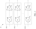
- FIG. 1 is a diagram illustrating a phased array such as a radio frequency (RF) phase-shifting phased array 10 according to an embodiment of the present invention.
- the RF phase-shifting phased array 10 may comprise multiple signal paths arranged in parallel, such as signal paths 100-1, 100-2, ..., and 100-N, where N may represent a positive integer.
- the signal path 100-1 may comprise a phase shifter PS 1 providing a phase shift ⁇ 1 and a gain equalizer GE 1 providing a tunable gain G 1
- the signal path 100-2 may comprise a phase shifter PS 2 providing a phase shift ⁇ 2 and a gain equalizer GE 2 providing a tunable gain G 2
- the signal path 100-N may comprise a phase shifter PS N providing a phase shift ⁇ N and a gain equalizer GE N providing a tunable gain G N .
- the phase shifters PS 1 , PS 1 , ..., and PS N may provide different gains.
- the gain equalizers GE 1 , GE 1 , ..., and GE N are configured to apply corresponding gains to signals on the paths 100-1, 100-2, ..., and 100-N, in order to compensate the gains provided by the phase shifters PS 1 , PS 1 , ..., and PS N .
- each of the gain equalizers GE 1 , GE 1 , ..., and GE N needs to be optimized, in order to make overall gains of the paths 100-1, 100-2, ..., and 100-N as much equal as possible.
- the gain equalizers GE 1 , GE 1 , ..., and GE N also provide phase shifts, however.
- phase shifts provided by the gain equalizers GE 1 , GE 1 , ..., and GE N it is preferable to minimize the phase shifts provided by the gain equalizers GE 1 , GE 1 , ..., and GE N , in order to prevent designs of the gain equalizers GE 1 , GE 1 , ..., and GE N and the phase shifters PS 1 , PS 1 , ..., and PS N from iterative modification.
- FIG. 2 is a diagram illustrating a gain equalizer 20 according to an embodiment of the present invention.
- the gain equalizer 20 may comprise a common source stage 110N and a transformer such as a balanced to unbalanced (Balun) transformer 130.
- the common source stage 110N is configured to apply a tunable gain to an input signal V IN , in order to generate an amplified signal
- the Balun transformer 130 is configured to convert the amplified signal into an output signal V OUT (e.g. converting a differential amplified signal generated by a differential architecture of the common source stage 110N into a single-ended output signal) on loading (illustrated by a resistor in figures for better comprehension) of next stage.
- the common source stage 110N may comprise a first input transistor and a second input transistor, such as input transistors MN1 and MN2, where the input transistors MN1 and MN2 are configured to receive the input signal V IN via gate terminals of the input transistors MN1 and MN2, respectively, and source terminals of the input transistors are coupled to a reference terminal such as a ground voltage terminal.
- the common source stage 110N may further comprise a first cascode transistor and a second cascode transistor, such as cascode transistors MN3 and MN4, where a source terminal of the cascode transistor MN3 is coupled to a drain terminal of the input transistor MN1, and a source terminal of the cascode transistor MN4 is coupled to a drain terminal of the input transistor MN2. Drain terminals of the cascode transistors MN3 and MN4 are coupled to the Balun transformer 130, and the cascode transistors MN3 and MN4 are configured to output the amplified signal via the drain terminals thereof.
- a switched-resistor tank may be coupled between the drain terminals of the.
- the Balun transformer 130 is implemented by inductors. Resistors within the switched-resistor tank and the inductors within the Balun transformer are different types of components, which means load caused by the Balun transformer 130 and load caused by the switched-resistor tank is unable to track each other, and thereby makes the tunable gain of the common source stage 110N be sensitive to process variation.
- gain step resolution and a tuning range of the tunable gain may vary over frequencies because the resistors and the inductors have different frequency responses, thereby impacting gain flatness.
- gain resolution and the tuning range may be required when adopting the switched-resistor tank, resulting that power consumption increases.
- one or more current-steering transistors may be coupled between the drain terminal of the cascode transistor MN3 and the source terminal of the cascode transistor MN4, and one or more current-steering transistors may be coupled between the drain terminal of the cascode transistor MN4 and the source terminal of the cascode transistor MN3.
- drain capacitances of these current-steering transistors may result in increase of overall output capacitive load of the common source stage 110N, which may further worsen the overall linearity of the gain equalizer 10, and increase of the overall power consumption may be required in order to meet similar linearity performance in comparison with an architecture without using these current-steering transistors.
- source terminals of current-steering transistors may be coupled to the source terminals of the cascode transistors MN3 and MN4, and drain terminals of these current-steering transistors may be coupled to a reference terminal.
- the tunable gain can be changed.
- the reference terminal is unable to be an ideal alternating current (AC) ground, and steered current of these current steering transistors flowing to this reference terminal may result in re-modulation, making this reference terminal become an interference source.
- the gain equalizer 20 may comprise a switch array 120N coupled between the source terminals of the cascode transistors MN3 and MN4, where the tunable gain can be controlled according to an equivalent impedance of the switch array 120N.
- the switch array 120N may comprise multiple switches such as SN 0 , SN 1 , ..., and SN M , and the switches SN 0 , SN 1 , ..., and SN M are connected in parallel between the source terminals of the cascode transistors MN3 and MN4, where M may represent a positive integer.
- the equivalent impedance of the switch array 120N can be determined by controlling whether any of the switches SN 0 , SN 1 , ..., and SN M is turned on or off.
- each of the switches SN 0 , SN 1 , ..., and SN M may be controlled by a corresponding bit of a digital code, where different values of this digital code may correspond to different combinations of turned-on switches among the switches SN 0 , SN 1 , ..., and SN M , thereby resulting in different equivalent impedances of the switch array 120N, respectively.
- a steered-away current flowing through the switch array 120N can be tunable, and an output current of the common source stage 110N flowing to the Balun transformer 130 can be tunable, resulting that the tunable gain of the gain equalizer 20 can be tunable.
- the switches SN 0 , SN 1 , ..., and SN M may have the same turned-on resistance (e.g. the switches SN 0 , SN 1 , ..., and SN M is implemented by the same size of transistors). In some embodiments, the switches SN 0 , SN 1 , ..., and SN M may have different turned-on resistances (e.g. the switches SN 0 , SN 1 , ..., and SN M is implemented by different sizes of transistors). In some embodiment, the digital code may be a binary code or a thermometer code.
- each of the input transistors MN1 and MN2 and the cascode transistors MN3 and MN4 is an N-type transistor such as an N-type Metal-Oxide-Semiconductor Field-Effect Transistor (NMOS), and each of the switches SN 0 , SN 1 , ..., and SN M may comprise an N-type transistor such as an NMOS.
- NMOS N-type Metal-Oxide-Semiconductor Field-Effect Transistor
- the current steered by the switch array 120N is substantially determined based on a device ratio of the transistors within the switch array 120N and the transistors (e.g. the cascode transistors MN3 and MN4) within the common source stage 110N, and is therefore less sensitive to the process variation.
- the switch array 120N configured for implementing a gain tuning function is placed at cascode source nodes of the common source stage 110N (i.e. the source terminals of the cascode transistors MN3 and MN4), which have relative low impedance in comparison with output nodes of the common source stage 110N (i.e. the drain terminals of the cascode transistors MN3 and MN4), a frequency response variation over gain gears (e.g.
- the switch array 120N does not increase the number of active devices at the output nodes of the common source stage 110N, impact to the linearity of the gain equalizer 20 caused by the switch array 120N can be minimized. Furthermore, the steered-away current flowing through the switch array 120N is steered away from one side of a differential architecture of the common source stage 110N to the other side of the differential architecture of the common source stage 110N, instead of being steering to a dedicated reference terminal, and the issue of re-modulation caused by the dedicated reference terminal can be avoided.
- FIG. 3 is a diagram illustrating a gain equalizer 30 according to another embodiment of the present invention.
- a common source stage 110P and a switch array 120P shown in FIG. 3 may be alternative designs of the common source stage 110N and a switch array 120N, respectively.
- the common source stage 110P may comprise input transistors MP1 and MP2 and cascode transistors MP3 and MP4.
- each of the input transistors MP1 and MP2 and the cascode transistors MP3 and MP4 may be a P-type transistor such as a P-type Metal-Oxide-Semiconductor Field-Effect Transistor (PMOS), and source terminals of the input transistors MP1 and MP2 are coupled to a supply voltage terminal VDD.
- the switch array 120P may comprise multiple switches such as SP1, SP2, ..., and SP M , where a main difference between the switch arrays 120N and 120P is that each of the switches SP1, SP2, ..., and SP M may comprise a P-type transistor such as a PMOS. Operations and advantages of the gain equalizer 30 are similar to the gain equalizer 20, related details are not repeated here for brevity.
- FIG. 4 is a diagram illustrating a gain equalizer 40 according to yet another embodiment of the present invention.
- the gain equalizer 40 may comprise the common source stages 110N and 110P, the switch arrays 120N and 120P, and the Balun transformer 130.
- all of the input transistors MN1, MN2, MP1 and MP2 are configured to receive the input signal V IN via gate terminals thereof, respectively, where the cascode transistor MP3 is coupled between the input transistor MP1 and the drain terminal of the cascode transistor MN3, and the cascode transistor MP4 is coupled between the input transistor MP2 and the drain terminal of the cascode transistor MN4.
- the common mode stages 110N and 110P may form a push-pull gain stage, which can improve a driving efficiency of the gain equalizer 40 in comparison with utilizing a single common source stage such as the embodiments of FIG. 2 and FIG. 3 .
- the switch array 120N is coupled between the source terminals of the cascode transistors MN3 and MN4, and the switch array 120P is coupled between the source terminals of the cascode transistors MP3 and MP4.
- a tunable gain of the gain equalizer 40 may be controlled according to equivalent impedances of the switch arrays 120N and 120P.
- each of the input transistors MN1 and MN2 and the cascode transistors MN3 and MN4 is an N-type transistor
- each switch within the switch array 120N may comprise an N-type transistor
- the current steered by the switch array 120N is substantially determined based on the device ratio of the transistors within the switch array 120N and the transistors (e.g. the cascode transistors MN3 and MN4) within the common source stage 110N.
- each of the input transistors MP1 and MP2 and the cascode transistors MP3 and MP4 is a P-type transistor
- each switch within the switch array 120P may comprise a P-type transistor
- the current steered by the switch array 120P is substantially determined based on the device ratio of the transistors within the switch array 120P and the transistors (e.g. the cascode transistors MP3 and MP4) within the common source stage 110P.
- the gain equalizer 40 may be regarded as a combined architecture of the gain equalizers 20 and 30, the advantages of the gain equalizers 20 and 30 can be included in the gain equalizer 40, and related details are omitted here for brevity.
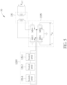
- FIG. 5 is a diagram illustrating a gain equalizer 50 according to still another embodiment of the present invention.
- the gain equalizer 50 is a special architecture which is obtained by changing the implementation of the switch array 120N based on the gain equalizer 20 shown in FIG. 2 .
- the switch array 120N may be replaced with a switch array 120N' which comprises multiple switch sub-arrays such as switch sub-arrays 120-1, 120-2, ..., and 120-K (labeled "Switch array” for brevity) connected in series, and an equivalent impedance of each switch sub-array of the switch sub-arrays 120-1, 120-2, ..., and 120-K is tunable, where K may represent a positive integer.
- each switch sub-array of the switch sub-arrays 120-1, 120-2, ..., and 120-K may comprise multiple switches connected in parallel between a first end (e.g. a right-side terminal illustrated in FIG. 5 ) and a second end (e.g. a left-side terminal illustrated in FIG. 5 ) of said each switch sub-array, and the switch sub-arrays 120-1, 120-2, ..., and 120-K are connected in series via the first end and the second end of said each switch sub-array, where the switch array 120N may be an example of any of the switch sub-arrays 120-1, 120-2, ..., and 120-K.
- the first end e.g.
- the right-side terminal) of the switch sub-array 120-1 is coupled to the source terminal of the cascode transistor MN3
- the first end (e.g. the right-side terminal) of the switch sub-array 120-2 is coupled to the second end (e.g. the left-side terminal) of the switch sub-array 120-1, and the rest may be deduced by analogy, where the second end (e.g. the left-side terminal) of the switch sub-array 120-K is coupled to the source terminal of the cascode transistor MN4.
- step resolution of tuning an overall equivalent impedance of the switch array 120N' can be improved in comparison with the embodiment of FIG. 2 , to thereby improve gain step resolution of a tunable gain of the gain equalizer 50.
- the number of switches within each of the switch sub-arrays 120-1, 120-2, ..., and 120-K may be the same. In some embodiment, the number of switches within each of the switch sub-arrays 120-1, 120-2, ..., and 120-K may be different from one another.
- FIG. 5 takes the architecture of utilizing N-type transistors as an example for illustration, but the present invention is not limited thereto. More particularly, the technique of improving the gain step resolution by connecting multiple switch sub-arrays in series as mentioned above can be adopted in the architecture of an N-type common source stage (e.g. the common source stage 110N shown in FIG.2 ), the architecture of a P-type common source stage (e.g.
- FIG. 6 is a diagram illustrating a working flow of a method for controlling a tunable gain of a gain equalizer according to an embodiment of the present invention, where the method is applicable to any of the gain equalizers 10, 20, 30, 40 and 50.
- the working flow shown in FIG. 6 is for illustrative purpose only, and is not meant to be a limitation of the present invention.
- one or more steps may be added, deleted or modified in the working flow shown in FIG. 6 .
- these steps do not have to be executed in the exact order shown in FIG. 6 .
- the gain equalizer may utilize a common source stage thereof to receive an input signal via gate terminals of a first input transistor and a second input transistor within the common source stage, respectively.
- the gain equalizer may utilize the common source stage to apply the tunable gain to the input signal for generating the amplified signal on drain terminals of a first cascode transistor and a second cascode transistor within the common source stage, respectively, wherein the first cascode transistor and the second cascode transistor are respectively coupled to the first input transistor and the second input transistor.
- the gain equalizer may utilize a switch array thereof to control the tunable gain according to an equivalent impedance of the switch array, wherein the switch array is coupled between respective source terminals of the first cascode transistor and the second cascode transistor.
- the gain equalizer and the associated method provided by the embodiments of the present invention implement the function of controlling the tunable gain of the gain equalizer by configuring a switch array coupled between the cascode source nodes of the common source amplifier within the gain equalizer, which can make the gain equalizer meet the requirements of the gain step resolution and the gain tuning range without introducing any side effects or in a way that is less likely to introduce side effects such as linearity issues, sensitivity issues related to process variation and frequency response variation over gain gears.
Landscapes
- Engineering & Computer Science (AREA)
- Power Engineering (AREA)
- Physics & Mathematics (AREA)
- Nonlinear Science (AREA)
- Control Of Amplification And Gain Control (AREA)
- Amplifiers (AREA)
Abstract
Description
- This application claims the benefit of
U.S. Provisional Application No. 63/352,342, filed on June 15th, 2022 - The present invention is related to gain equalization, and more particularly, to a gain equalizer and a method for controlling a tunable gain of the gain equalizer.
- Gain equalizers are typically placed in parallel signal paths for compensating gain variation caused by some path settings and the phase-shifting operation. It is preferable to design a gain equalizer with fine gain step resolution, a wide gain tuning range and small phase variation for different gain settings. In practice, the design of the gain equalizer may face several challenges when some blocks are added into the gain equalizer for achieving the design requirements mentioned above. For example, these blocks may result in that absolute gain values, gain flatness over frequencies, linearity noise related performance, etc., may be sensitive to process variation, and the overall power consumption may be greatly increased in order to ensure that the specifications mentioned above can meet the targets under all process corners.
- Thus, there is a need for a novel architecture of the gain equalizer and an associated method, which can make the gain equalizer meet the design requirements without introducing any side effects or in a way that is less likely to introduce side effects.
- An objective of the present invention is to provide a gain equalizer and a method for controlling a tunable gain of the gain equalizer, in order to optimize overall performance of the gain equalizer (which includes gain step resolution, gain tuning range, minimized phase variation with respect to different gain settings, etc.) without worsening performance related to gain precision, gain flatness, linearity, noise, etc.
- At least one embodiment of the present invention provides a gain equalizer. The gain equalizer comprises a first common source stage and a first switch array. The first common source stage is configured to apply a tunable gain to an input signal, in order to generate an amplified signal. The first common source stage comprises a first input transistor, a second input transistor, a first cascode transistor and a second cascode transistor, wherein the first cascode transistor and the second cascode transistor are respectively coupled to the first input transistor and the second input transistor. The first input transistor and the second input transistor are configured to receive the input signal via gate terminals of the first input transistor and the second input transistor, respectively, and the first cascode transistor and the second cascode transistor are configured to output the amplified signal via drain terminals of the first cascode transistor and the second cascode transistor, respectively. In addition, the first switch array is coupled between respective source terminals of the first cascode transistor and the second cascode transistor, wherein the tunable gain is controlled according to an equivalent impedance of the first switch array.
- At least one embodiment of the present invention provides a method for controlling a tunable gain of a gain equalizer. The method comprises: utilizing a first common source stage of the gain equalizer to receive an input signal via gate terminals of a first input transistor and a second input transistor within the first common source stage, respectively; utilizing the first common source stage to apply the tunable gain to the input signal for generating the amplified signal on drain terminals of a first cascode transistor and a second cascode transistor within the first common source stage, respectively, wherein the first cascode transistor and the second cascode transistor are respectively coupled to the first input transistor and the second input transistor; and utilizing a first switch array of the gain equalizer to control the tunable gain according to an equivalent impedance of the first switch array, wherein the first switch array is coupled between respective source terminals of the first cascode transistor and the second cascode transistor.
- The gain equalizer and the method provided by the embodiments of the present invention utilize a switch array to split output current for controlling the tunable gain. As the switch array is not placed at output nodes of a gain stage of the gain equalizer, frequency response of the gain equalizer will not be greatly impacted by the switch array. In addition, the switch array is not coupled to additional power supply terminal, and a re-modulation issue is therefore avoided.
- These and other objectives of the present invention will no doubt become obvious to those of ordinary skill in the art after reading the following detailed description of the preferred embodiment that is illustrated in the various figures and drawings.
-
-
FIG. 1 is a diagram illustrating a phased array according to an embodiment of the present invention. -
FIG. 2 is a diagram illustrating a gain equalizer according to an embodiment of the present invention. -
FIG. 3 is a diagram illustrating a gain equalizer according to another embodiment of the present invention. -
FIG. 4 is a diagram illustrating a gain equalizer according to yet another embodiment of the present invention. -
FIG. 5 is a diagram illustrating a gain equalizer according to still another embodiment of the present invention. -
FIG. 6 is a diagram illustrating a working flow of a method for controlling a tunable gain of a gain equalizer according to an embodiment of the present invention. - Certain terms are used throughout the following description and claims, which refer to particular components. As one skilled in the art will appreciate, electronic equipment manufacturers may refer to a component by different names. This document does not intend to distinguish between components that differ in name but not in function. In the following description and in the claims, the terms "include" and "comprise" are used in an open-ended fashion, and thus should be interpreted to mean "include, but not limited to ...". Also, the term "couple" is intended to mean either an indirect or direct electrical connection. Accordingly, if one device is coupled to another device, that connection may be through a direct electrical connection, or through an indirect electrical connection via other devices and connections.
-
FIG. 1 is a diagram illustrating a phased array such as a radio frequency (RF) phase-shiftingphased array 10 according to an embodiment of the present invention. As shown inFIG. 1 , the RF phase-shiftingphased array 10 may comprise multiple signal paths arranged in parallel, such as signal paths 100-1, 100-2, ..., and 100-N, where N may represent a positive integer. In this embodiment, the signal path 100-1 may comprise a phase shifter PS1 providing a phase shift Φ1 and a gain equalizer GE1 providing a tunable gain G1, and the signal path 100-2 may comprise a phase shifter PS2 providing a phase shift Φ2 and a gain equalizer GE2 providing a tunable gain G2, where the rest may be deduced by analogy, for example, the signal path 100-N may comprise a phase shifter PSN providing a phase shift ΦN and a gain equalizer GEN providing a tunable gain GN. In practice, in addition to different phase shifts Φ1, Φ1, ..., and ΦN, the phase shifters PS1, PS1, ..., and PSN may provide different gains. Thus, the gain equalizers GE1, GE1, ..., and GEN are configured to apply corresponding gains to signals on the paths 100-1, 100-2, ..., and 100-N, in order to compensate the gains provided by the phase shifters PS1, PS1, ..., and PSN. Thus, gain precision, gain step resolution and gain tuning range of each of the gain equalizers GE1, GE1, ..., and GEN needs to be optimized, in order to make overall gains of the paths 100-1, 100-2, ..., and 100-N as much equal as possible. In practice, the gain equalizers GE1, GE1, ..., and GEN also provide phase shifts, however. Thus, it is preferable to minimize the phase shifts provided by the gain equalizers GE1, GE1, ..., and GEN, in order to prevent designs of the gain equalizers GE1, GE1, ..., and GEN and the phase shifters PS1, PS1, ..., and PSN from iterative modification. -
FIG. 2 is a diagram illustrating again equalizer 20 according to an embodiment of the present invention. As shown inFIG. 2 , thegain equalizer 20 may comprise acommon source stage 110N and a transformer such as a balanced to unbalanced (Balun)transformer 130. Thecommon source stage 110N is configured to apply a tunable gain to an input signal VIN, in order to generate an amplified signal, and the Baluntransformer 130 is configured to convert the amplified signal into an output signal VOUT (e.g. converting a differential amplified signal generated by a differential architecture of thecommon source stage 110N into a single-ended output signal) on loading (illustrated by a resistor in figures for better comprehension) of next stage. In detail, thecommon source stage 110N may comprise a first input transistor and a second input transistor, such as input transistors MN1 and MN2, where the input transistors MN1 and MN2 are configured to receive the input signal VIN via gate terminals of the input transistors MN1 and MN2, respectively, and source terminals of the input transistors are coupled to a reference terminal such as a ground voltage terminal. Thecommon source stage 110N may further comprise a first cascode transistor and a second cascode transistor, such as cascode transistors MN3 and MN4, where a source terminal of the cascode transistor MN3 is coupled to a drain terminal of the input transistor MN1, and a source terminal of the cascode transistor MN4 is coupled to a drain terminal of the input transistor MN2. Drain terminals of the cascode transistors MN3 and MN4 are coupled to the Baluntransformer 130, and the cascode transistors MN3 and MN4 are configured to output the amplified signal via the drain terminals thereof. - In some embodiments, a switched-resistor tank may be coupled between the drain terminals of the. By changing an overall resistance of the switched-resistor tank in order to change an overall output load of the
common source stage 110N, the tunable gain can be changed. The Baluntransformer 130 is implemented by inductors. Resistors within the switched-resistor tank and the inductors within the Balun transformer are different types of components, which means load caused by theBalun transformer 130 and load caused by the switched-resistor tank is unable to track each other, and thereby makes the tunable gain of thecommon source stage 110N be sensitive to process variation. In addition, gain step resolution and a tuning range of the tunable gain may vary over frequencies because the resistors and the inductors have different frequency responses, thereby impacting gain flatness. Thus, over design regarding both of the gain resolution and the tuning range may be required when adopting the switched-resistor tank, resulting that power consumption increases. - In some embodiment, one or more current-steering transistors may be coupled between the drain terminal of the cascode transistor MN3 and the source terminal of the cascode transistor MN4, and one or more current-steering transistors may be coupled between the drain terminal of the cascode transistor MN4 and the source terminal of the cascode transistor MN3. By changing the number of enabled transistor among these current-steering, the tunable gain can be changed. These current-steering transistors are nonlinear components, which may worsen an overall linearity of the
gain equalizer 10. In addition, drain capacitances of these current-steering transistors may result in increase of overall output capacitive load of thecommon source stage 110N, which may further worsen the overall linearity of thegain equalizer 10, and increase of the overall power consumption may be required in order to meet similar linearity performance in comparison with an architecture without using these current-steering transistors. - In some embodiment, source terminals of current-steering transistors may be coupled to the source terminals of the cascode transistors MN3 and MN4, and drain terminals of these current-steering transistors may be coupled to a reference terminal. By changing the number of enabled transistor among these current-steering, in order to change current flowing through output of the
common source stage 110N, the tunable gain can be changed. As these current-steering transistors is not directly connected to the drain terminals of the drain terminals of the transistors MN3 and MN4, overall output load of thecommon source stage 110N is less impacted. There are still some disadvantages, however. In practice, the reference terminal is unable to be an ideal alternating current (AC) ground, and steered current of these current steering transistors flowing to this reference terminal may result in re-modulation, making this reference terminal become an interference source. - In the embodiment of
FIG. 2 , thegain equalizer 20 may comprise aswitch array 120N coupled between the source terminals of the cascode transistors MN3 and MN4, where the tunable gain can be controlled according to an equivalent impedance of theswitch array 120N. In particular, theswitch array 120N may comprise multiple switches such as SN0, SN1, ..., and SNM, and the switches SN0, SN1, ..., and SNM are connected in parallel between the source terminals of the cascode transistors MN3 and MN4, where M may represent a positive integer. In this embodiment, the equivalent impedance of theswitch array 120N can be determined by controlling whether any of the switches SN0, SN1, ..., and SNM is turned on or off. For example, each of the switches SN0, SN1, ..., and SNM may be controlled by a corresponding bit of a digital code, where different values of this digital code may correspond to different combinations of turned-on switches among the switches SN0, SN1, ..., and SNM, thereby resulting in different equivalent impedances of theswitch array 120N, respectively. As the equivalent impedances of theswitch array 120N is tunable, a steered-away current flowing through theswitch array 120N can be tunable, and an output current of thecommon source stage 110N flowing to theBalun transformer 130 can be tunable, resulting that the tunable gain of thegain equalizer 20 can be tunable. - In some embodiments, the switches SN0, SN1, ..., and SNM may have the same turned-on resistance (e.g. the switches SN0, SN1, ..., and SNM is implemented by the same size of transistors). In some embodiments, the switches SN0, SN1, ..., and SNM may have different turned-on resistances (e.g. the switches SN0, SN1, ..., and SNM is implemented by different sizes of transistors). In some embodiment, the digital code may be a binary code or a thermometer code.
- It should be noted that all devices within the
switch array 120N are active devices. In detail, each of the input transistors MN1 and MN2 and the cascode transistors MN3 and MN4 is an N-type transistor such as an N-type Metal-Oxide-Semiconductor Field-Effect Transistor (NMOS), and each of the switches SN0, SN1, ..., and SNM may comprise an N-type transistor such as an NMOS. As all devices within theswitch array 120N and all devices within thecommon source stage 110N are implemented with the same type of devices (e.g. N-type transistors), electronic behaviors of theswitch array 120N can track the electronic behaviors of thecommon source stage 110N over process variation. Thus, the current steered by theswitch array 120N is substantially determined based on a device ratio of the transistors within theswitch array 120N and the transistors (e.g. the cascode transistors MN3 and MN4) within thecommon source stage 110N, and is therefore less sensitive to the process variation. In addition, as theswitch array 120N configured for implementing a gain tuning function is placed at cascode source nodes of thecommon source stage 110N (i.e. the source terminals of the cascode transistors MN3 and MN4), which have relative low impedance in comparison with output nodes of thecommon source stage 110N (i.e. the drain terminals of the cascode transistors MN3 and MN4), a frequency response variation over gain gears (e.g. over different gain settings of the tunable gain) of thegain equalizer 20 can be minimized. As theswitch array 120N does not increase the number of active devices at the output nodes of thecommon source stage 110N, impact to the linearity of thegain equalizer 20 caused by theswitch array 120N can be minimized. Furthermore, the steered-away current flowing through theswitch array 120N is steered away from one side of a differential architecture of thecommon source stage 110N to the other side of the differential architecture of thecommon source stage 110N, instead of being steering to a dedicated reference terminal, and the issue of re-modulation caused by the dedicated reference terminal can be avoided. -
FIG. 3 is a diagram illustrating again equalizer 30 according to another embodiment of the present invention. In comparison with thegain equalizer 20 shown inFIG. 2 , acommon source stage 110P and aswitch array 120P shown inFIG. 3 may be alternative designs of thecommon source stage 110N and aswitch array 120N, respectively. As shown inFIG. 3 , thecommon source stage 110P may comprise input transistors MP1 and MP2 and cascode transistors MP3 and MP4. Main differences between the common source stages 110N and 110P are that each of the input transistors MP1 and MP2 and the cascode transistors MP3 and MP4 may be a P-type transistor such as a P-type Metal-Oxide-Semiconductor Field-Effect Transistor (PMOS), and source terminals of the input transistors MP1 and MP2 are coupled to a supply voltage terminal VDD. Theswitch array 120P may comprise multiple switches such as SP1, SP2, ..., and SPM, where a main difference between theswitch arrays gain equalizer 30 are similar to thegain equalizer 20, related details are not repeated here for brevity. -
FIG. 4 is a diagram illustrating again equalizer 40 according to yet another embodiment of the present invention. As shown inFIG. 4 , thegain equalizer 40 may comprise the common source stages 110N and 110P, theswitch arrays Balun transformer 130. In this embodiment, all of the input transistors MN1, MN2, MP1 and MP2 are configured to receive the input signal VIN via gate terminals thereof, respectively, where the cascode transistor MP3 is coupled between the input transistor MP1 and the drain terminal of the cascode transistor MN3, and the cascode transistor MP4 is coupled between the input transistor MP2 and the drain terminal of the cascode transistor MN4. Thus, thecommon mode stages gain equalizer 40 in comparison with utilizing a single common source stage such as the embodiments ofFIG. 2 andFIG. 3 . Based on the architecture of the push-pull gain stage, theswitch array 120N is coupled between the source terminals of the cascode transistors MN3 and MN4, and theswitch array 120P is coupled between the source terminals of the cascode transistors MP3 and MP4. Thus, a tunable gain of thegain equalizer 40 may be controlled according to equivalent impedances of theswitch arrays - In this embodiment, as each of the input transistors MN1 and MN2 and the cascode transistors MN3 and MN4 is an N-type transistor, and each switch within the
switch array 120N may comprise an N-type transistor, the current steered by theswitch array 120N is substantially determined based on the device ratio of the transistors within theswitch array 120N and the transistors (e.g. the cascode transistors MN3 and MN4) within thecommon source stage 110N. In addition, as each of the input transistors MP1 and MP2 and the cascode transistors MP3 and MP4 is a P-type transistor, and each switch within theswitch array 120P may comprise a P-type transistor, the current steered by theswitch array 120P is substantially determined based on the device ratio of the transistors within theswitch array 120P and the transistors (e.g. the cascode transistors MP3 and MP4) within thecommon source stage 110P. As thegain equalizer 40 may be regarded as a combined architecture of thegain equalizers gain equalizers gain equalizer 40, and related details are omitted here for brevity. -
FIG. 5 is a diagram illustrating again equalizer 50 according to still another embodiment of the present invention. Thegain equalizer 50 is a special architecture which is obtained by changing the implementation of theswitch array 120N based on thegain equalizer 20 shown inFIG. 2 . In detail, theswitch array 120N may be replaced with aswitch array 120N' which comprises multiple switch sub-arrays such as switch sub-arrays 120-1, 120-2, ..., and 120-K (labeled "Switch array" for brevity) connected in series, and an equivalent impedance of each switch sub-array of the switch sub-arrays 120-1, 120-2, ..., and 120-K is tunable, where K may represent a positive integer. For example, each switch sub-array of the switch sub-arrays 120-1, 120-2, ..., and 120-K may comprise multiple switches connected in parallel between a first end (e.g. a right-side terminal illustrated inFIG. 5 ) and a second end (e.g. a left-side terminal illustrated inFIG. 5 ) of said each switch sub-array, and the switch sub-arrays 120-1, 120-2, ..., and 120-K are connected in series via the first end and the second end of said each switch sub-array, where theswitch array 120N may be an example of any of the switch sub-arrays 120-1, 120-2, ..., and 120-K. As shown inFIG. 1 , the first end (e.g. the right-side terminal) of the switch sub-array 120-1 is coupled to the source terminal of the cascode transistor MN3, the first end (e.g. the right-side terminal) of the switch sub-array 120-2 is coupled to the second end (e.g. the left-side terminal) of the switch sub-array 120-1, and the rest may be deduced by analogy, where the second end (e.g. the left-side terminal) of the switch sub-array 120-K is coupled to the source terminal of the cascode transistor MN4. Based on the architecture of the switch array comprising the switch sub-arrays 120-1, 120-2, ..., and 120-K connected in series, step resolution of tuning an overall equivalent impedance of theswitch array 120N' can be improved in comparison with the embodiment ofFIG. 2 , to thereby improve gain step resolution of a tunable gain of thegain equalizer 50. - In some embodiment, the number of switches within each of the switch sub-arrays 120-1, 120-2, ..., and 120-K may be the same. In some embodiment, the number of switches within each of the switch sub-arrays 120-1, 120-2, ..., and 120-K may be different from one another. It should be noted that the embodiment of
FIG. 5 takes the architecture of utilizing N-type transistors as an example for illustration, but the present invention is not limited thereto. More particularly, the technique of improving the gain step resolution by connecting multiple switch sub-arrays in series as mentioned above can be adopted in the architecture of an N-type common source stage (e.g. thecommon source stage 110N shown inFIG.2 ), the architecture of a P-type common source stage (e.g. thecommon source stage 110P shown inFIG.3 ) and the architecture of a push-pull gain stage (e.g. the push-pull gain stage comprising the common source stages 110N and 110P shown inFIG. 4 ). Those skilled in this art should understand how to adopt this technique in different topologies according to the above descriptions, and related details are omitted here for brevity. -
FIG. 6 is a diagram illustrating a working flow of a method for controlling a tunable gain of a gain equalizer according to an embodiment of the present invention, where the method is applicable to any of thegain equalizers FIG. 6 is for illustrative purpose only, and is not meant to be a limitation of the present invention. For example, one or more steps may be added, deleted or modified in the working flow shown inFIG. 6 . In addition, if an overall result is not hindered, these steps do not have to be executed in the exact order shown inFIG. 6 . - In Step S610, the gain equalizer may utilize a common source stage thereof to receive an input signal via gate terminals of a first input transistor and a second input transistor within the common source stage, respectively.
- In Step S620, the gain equalizer may utilize the common source stage to apply the tunable gain to the input signal for generating the amplified signal on drain terminals of a first cascode transistor and a second cascode transistor within the common source stage, respectively, wherein the first cascode transistor and the second cascode transistor are respectively coupled to the first input transistor and the second input transistor.
- In Step S630, the gain equalizer may utilize a switch array thereof to control the tunable gain according to an equivalent impedance of the switch array, wherein the switch array is coupled between respective source terminals of the first cascode transistor and the second cascode transistor.
- To summarize, the gain equalizer and the associated method provided by the embodiments of the present invention implement the function of controlling the tunable gain of the gain equalizer by configuring a switch array coupled between the cascode source nodes of the common source amplifier within the gain equalizer, which can make the gain equalizer meet the requirements of the gain step resolution and the gain tuning range without introducing any side effects or in a way that is less likely to introduce side effects such as linearity issues, sensitivity issues related to process variation and frequency response variation over gain gears.
- Those skilled in the art will readily observe that numerous modifications and alterations of the device and method may be made while retaining the teachings of the invention. Accordingly, the above disclosure should be construed as limited only by the metes and bounds of the appended claims.
- The present application may also be defined by the following numbered clauses.
- 1. A gain equalizer, comprising:
- a first common source stage, configured to apply a tunable gain to an input signal, in order to generate an amplified signal, wherein the first common source stage comprises:
- a first input transistor and a second input transistor, configured to receive the input signal via gate terminals of the first input transistor and the second input transistor, respectively; and
- a first cascode transistor and a second cascode transistor, respectively coupled to the first input transistor and the second input transistor, configured to output the amplified signal via drain terminals of the first cascode transistor and the second cascode transistor, respectively; and
- a first switch array, coupled between respective source terminals of the first cascode transistor and the second cascode transistor, wherein the tunable gain is controlled according to an equivalent impedance of the first switch array.
- a first common source stage, configured to apply a tunable gain to an input signal, in order to generate an amplified signal, wherein the first common source stage comprises:
- 2. The gain equalizer of clause 1, wherein the first switch array comprises multiple switches, and the multiple switches are connected in parallel between the respective source terminals of the first cascode transistor and the second cascode transistor.
- 3. The gain equalizer of
clause 2, wherein the equivalent impedance of the first switch array is determined by controlling whether any of the multiple switches is turned on or off. - 4. The gain equalizer of
clause 2, wherein each of the first input transistor, the second input transistor, the first cascode transistor and the second cascode transistor is an N-type transistor, and each of the multiple switches comprises an N-type transistor. - 5. The gain equalizer of
clause 2, wherein each of the first input transistor, the second input transistor, the first cascode transistor and the second cascode transistor is a P-type transistor, and each of the multiple switches comprises a P-type transistor. - 6. The gain equalizer of clause 1, further comprising:
- a second common source stage, comprising:
- a third input transistor and a fourth input transistor, configured to receive the input signal via gate terminals of the third input transistor and the fourth input transistor, respectively; and
- a third cascode transistor and a fourth cascode transistor, wherein the third cascode transistor is coupled between the third input transistor and the drain terminal of the first cascode transistor, and the fourth cascode transistor is coupled between the fourth input transistor and the drain terminal of the second cascode transistor; and
- a second switch array, coupled between respective source terminals of the third cascode transistor and the fourth cascode transistor, wherein the tunable gain is further controlled according to an equivalent impedance of the second switch array.
- a second common source stage, comprising:
- 7. The gain equalizer of clause 6, wherein each of the first input transistor, the second input transistor, the first cascode transistor and the second cascode transistor is an N-type transistor, each switch within the first switch array comprises an N-type transistor, each of the third input transistor, the fourth input transistor, the third cascode transistor and the fourth cascode transistor is a P-type transistor, and each switch within the second switch array comprises a P-type transistor.
- 8. The gain equalizer of clause 1, wherein the first switch array comprises multiple switch sub-arrays connected in series, and an equivalent impedance of each switch sub-array of the multiple switch sub-arrays is tunable.
- 9. The gain equalizer of clause 8, wherein said each switch sub-array comprises multiple switches connected in parallel between a first end and a second end of said each switch sub-array, and the multiple switch sub-arrays are connected in series via the first end and the second end of said each switch sub-array.
- 10. The gain equalizer of clause 1, further comprising:
a transformer, coupled to the drain terminals of the first cascode transistor and the second cascode transistor, configured to convert the amplified signal into an output signal. - 11. A method for controlling a tunable gain of a gain equalizer, comprising:
- utilizing a first common source stage of the gain equalizer to receive an input signal via gate terminals of a first input transistor and a second input transistor within the first common source stage, respectively;
- utilizing the first common source stage to apply the tunable gain to the input signal for generating the amplified signal on drain terminals of a first cascode transistor and a second cascode transistor within the first common source stage, respectively, wherein the first cascode transistor and the second cascode transistor are respectively coupled to the first input transistor and the second input transistor; and
- utilizing a first switch array of the gain equalizer to control the tunable gain according to an equivalent impedance of the first switch array, wherein the first switch array is coupled between respective source terminals of the first cascode transistor and the second cascode transistor.
- 12. The method of clause 11, wherein the first switch array comprises multiple switches, and the multiple switches are connected in parallel between the respective source terminals of the first cascode transistor and the second cascode transistor.
- 13. The method of clause 12, wherein the equivalent impedance of the first switch array is determined by controlling whether any of the multiple switches is turned on or off.
- 14. The method of clause 12, wherein each of the first input transistor, the second input transistor, the first cascode transistor and the second cascode transistor is an N-type transistor, and each of the multiple switches comprises an N-type transistor.
- 15. The method of clause 12, wherein each of the first input transistor, the second input transistor, the first cascode transistor and the second cascode transistor is a P-type transistor, and each of the multiple switches comprises a P-type transistor.
- 16. The method of clause 11, further comprising:
- receiving the input signal via gate terminals of a third input transistor and a fourth input transistor within a second common source stage, respectively, wherein a third cascode transistor within the second common source stage is coupled between the third input transistor and the drain terminal of the first cascode transistor, and a fourth cascode transistor within the second common source stage is coupled between the fourth input transistor and the drain terminal of the second cascode transistor; and
- utilizing a second switch array of the gain equalizer to further control the tunable gain according to an equivalent impedance of the second switch array, wherein the second switch array is coupled between respective source terminals of the third cascode transistor and the fourth cascode transistor, wherein the tunable gain is further controlled according to an equivalent impedance of the second switch array.
- 17. The method of clause 16, wherein each of the first input transistor, the second input transistor, the first cascode transistor and the second cascode transistor is an N-type transistor, each switch within the first switch array comprises an N-type transistor, each of the third input transistor, the fourth input transistor, the third cascode transistor and the fourth cascode transistor is a P-type transistor, and each switch within the second switch array comprises a P-type transistor.
- 18. The method of clause 11, wherein the first switch array comprises multiple switch sub-arrays connected in series, and an equivalent impedance of each switch sub-array of the multiple switch sub-arrays is tunable.
- 19. The method of clause 18, wherein said each switch sub-array comprises multiple switches connected in parallel between a first end and a second end of said each switch sub-array, and the multiple switch sub-arrays are connected in series via the first end and the second end of said each switch sub-array.
- 20. The method of clause 11, further comprising:
utilizing a transformer coupled to the drain terminals of the first cascode transistor and the second cascode transistor to convert the amplified signal into an output signal.
Claims (15)
- A gain equalizer (10, 20, 30, 40, 50), comprising:a first common source stage (110n, 110p), configured to apply a tunable gain to an input signal, in order to generate an amplified signal, wherein the first common source stage (110n, 110p) comprises:a first input transistor and a second input transistor, configured to receive the input signal via gate terminals of the first input transistor and the second input transistor, respectively; anda first cascode transistor and a second cascode transistor, respectively coupled to the first input transistor and the second input transistor, configured to output the amplified signal via drain terminals of the first cascode transistor and the second cascode transistor, respectively; anda first switch array (120n, 120n', 120p), coupled between respective source terminals of the first cascode transistor and the second cascode transistor, wherein the tunable gain is controlled according to an equivalent impedance of the first switch array (120n, 120n', 120p).
- The gain equalizer (10, 20, 30, 40, 50) of claim 1, wherein the first switch array (120n, 120n', 120p) comprises multiple switches, and the multiple switches are connected in parallel between the respective source terminals of the first cascode transistor and the second cascode transistor.
- The gain equalizer (10, 20, 30, 40, 50) of claim 2, wherein the equivalent impedance of the first switch array (120n, 120n', 120p) is determined by controlling whether any of the multiple switches is turned on or off; orwherein each of the first input transistor, the second input transistor, the first cascode transistor and the second cascode transistor is an N-type transistor, and each of the multiple switches comprises an N-type transistor; orwherein each of the first input transistor, the second input transistor, the first cascode transistor and the second cascode transistor is a P-type transistor, and each of the multiple switches comprises a P-type transistor.
- The gain equalizer (10, 20, 30, 40, 50) of claim 1, further comprising:a second common source stage (110n, 110p), comprising:a third input transistor and a fourth input transistor, configured to receive the input signal via gate terminals of the third input transistor and the fourth input transistor, respectively; anda third cascode transistor and a fourth cascode transistor, wherein the third cascode transistor is coupled between the third input transistor and the drain terminal of the first cascode transistor, and the fourth cascode transistor is coupled between the fourth input transistor and the drain terminal of the second cascode transistor; anda second switch array (120n, 120n', 120p), coupled between respective source terminals of the third cascode transistor and the fourth cascode transistor, wherein the tunable gain is further controlled according to an equivalent impedance of the second switch array (120n, 120n', 120p).
- The gain equalizer (10, 20, 30, 40, 50) of claim 4, wherein each of the first input transistor, the second input transistor, the first cascode transistor and the second cascode transistor is an N-type transistor, each switch within the first switch array (120n, 120n', 120p) comprises an N-type transistor, each of the third input transistor, the fourth input transistor, the third cascode transistor and the fourth cascode transistor is a P-type transistor, and each switch within the second switch array (120n, 120n', 120p) comprises a P-type transistor.
- The gain equalizer (10, 20, 30, 40, 50) of claim 1, wherein the first switch array (120n, 120n', 120p) comprises multiple switch sub-arrays (120-1, 120-2, 120-k) connected in series, and an equivalent impedance of each switch sub-array (120-1, 120-2, 120-k) of the multiple switch sub-arrays (120-1, 120-2, 120-k) is tunable.
- The gain equalizer (10, 20, 30, 40, 50) of claim 6, wherein said each switch sub-array (120-1, 120-2, 120-k) comprises multiple switches connected in parallel between a first end and a second end of said each switch sub-array (120-1, 120-2, 120-k), and the multiple switch sub-arrays (120-1, 120-2, 120-k) are connected in series via the first end and the second end of said each switch sub-array (120-1, 120-2, 120-k).
- The gain equalizer (10, 20, 30, 40, 50) of claim 1, further comprising:
a transformer, coupled to the drain terminals of the first cascode transistor and the second cascode transistor, configured to convert the amplified signal into an output signal. - A method for controlling a tunable gain of a gain equalizer (10, 20, 30, 40, 50), comprising:utilizing a first common source stage (110n, 110p) of the gain equalizer (10, 20, 30, 40, 50) to receive an input signal via gate terminals of a first input transistor and a second input transistor within the first common source stage (110n, 110p), respectively;utilizing the first common source stage (110n, 110p) to apply the tunable gain to the input signal for generating the amplified signal on drain terminals of a first cascode transistor and a second cascode transistor within the first common source stage (110n, 110p), respectively, wherein the first cascode transistor and the second cascode transistor are respectively coupled to the first input transistor and the second input transistor; andutilizing a first switch array (120n, 120n', 120p) of the gain equalizer (10, 20, 30, 40, 50) to control the tunable gain according to an equivalent impedance of the first switch array (120n, 120n', 120p), wherein the first switch array (120n, 120n', 120p) is coupled between respective source terminals of the first cascode transistor and the second cascode transistor.
- The method of claim 9, wherein the first switch array (120n, 120n', 120p) comprises multiple switches, and the multiple switches are connected in parallel between the respective source terminals of the first cascode transistor and the second cascode transistor.
- The method of claim 10, wherein the equivalent impedance of the first switch array (120n, 120n', 120p) is determined by controlling whether any of the multiple switches is turned on or off; orwherein each of the first input transistor, the second input transistor, the first cascode transistor and the second cascode transistor is an N-type transistor, and each of the multiple switches comprises an N-type transistor; orwherein each of the first input transistor, the second input transistor, the first cascode transistor and the second cascode transistor is a P-type transistor, and each of the multiple switches comprises a P-type transistor.
- The method of claim 9, further comprising:receiving the input signal via gate terminals of a third input transistor and a fourth input transistor within a second common source stage (110n, 110p), respectively, wherein a third cascode transistor within the second common source stage (110n, 110p) is coupled between the third input transistor and the drain terminal of the first cascode transistor, and a fourth cascode transistor within the second common source stage (110n, 110p) is coupled between the fourth input transistor and the drain terminal of the second cascode transistor; andutilizing a second switch array (120n, 120n', 120p) of the gain equalizer (10, 20, 30, 40, 50) to further control the tunable gain according to an equivalent impedance of the second switch array (120n, 120n', 120p), wherein the second switch array (120n, 120n', 120p) is coupled between respective source terminals of the third cascode transistor and the fourth cascode transistor, wherein the tunable gain is further controlled according to an equivalent impedance of the second switch array (120n, 120n', 120p).
- The method of claim 12, wherein each of the first input transistor, the second input transistor, the first cascode transistor and the second cascode transistor is an N-type transistor, each switch within the first switch array (120n, 120n', 120p) comprises an N-type transistor, each of the third input transistor, the fourth input transistor, the third cascode transistor and the fourth cascode transistor is a P-type transistor, and each switch within the second switch array (120n, 120n', 120p) comprises a P-type transistor.
- The method of claim 9, wherein the first switch array (120n, 120n', 120p) comprises multiple switch sub-arrays (120-1, 120-2, 120-k) connected in series, and an equivalent impedance of each switch sub-array (120-1, 120-2, 120-k) of the multiple switch sub-arrays (120-1, 120-2, 120-k) is tunable.
- The method of claim 14, wherein said each switch sub-array (120-1, 120-2, 120-k) comprises multiple switches connected in parallel between a first end and a second end of said each switch sub-array (120-1, 120-2, 120-k), and the multiple switch sub-arrays (120-1, 120-2, 120-k) are connected in series via the first end and the second end of said each switch sub-array (120-1, 120-2, 120-k).
Applications Claiming Priority (2)
| Application Number | Priority Date | Filing Date | Title |
|---|---|---|---|
| US202263352342P | 2022-06-15 | 2022-06-15 | |
| US18/086,600 US12580541B2 (en) | 2022-06-15 | 2022-12-21 | Gain equalizer and method for controlling tunable gain of gain equalizer |
Publications (1)
| Publication Number | Publication Date |
|---|---|
| EP4293903A1 true EP4293903A1 (en) | 2023-12-20 |
Family
ID=85158711
Family Applications (1)
| Application Number | Title | Priority Date | Filing Date |
|---|---|---|---|
| EP23154459.4A Pending EP4293903A1 (en) | 2022-06-15 | 2023-02-01 | Gain equalizer and method for controlling tunable gain of gain equalizer |
Country Status (3)
| Country | Link |
|---|---|
| US (1) | US12580541B2 (en) |
| EP (1) | EP4293903A1 (en) |
| TW (1) | TWI866285B (en) |
Citations (3)
| Publication number | Priority date | Publication date | Assignee | Title |
|---|---|---|---|---|
| US20060071712A1 (en) * | 2004-10-04 | 2006-04-06 | Samsung Electronics Co.,Ltd. | Variable gain amplifier |
| US20180302051A1 (en) * | 2017-04-13 | 2018-10-18 | Futurewei Technologies, Inc. | Programmable gain stage based on width ratio of two mosfets |
| US10110177B1 (en) * | 2017-07-28 | 2018-10-23 | Silicon Laboratories Inc. | Programmable impedance control for a transformer |
Family Cites Families (4)
| Publication number | Priority date | Publication date | Assignee | Title |
|---|---|---|---|---|
| US7292102B2 (en) * | 2004-09-10 | 2007-11-06 | Broadcom Corporation | Gain control scheme independent of process, voltage and temperature |
| US7586458B2 (en) * | 2007-03-19 | 2009-09-08 | Ahmadreza Rofougaran | Method and system for using a transformer for FM transmit and FM receive functionality |
| EP3940953A4 (en) * | 2019-03-30 | 2022-03-09 | Huawei Technologies Co., Ltd. | VARIABLE GAIN AMPLIFIER AND PHASE CONTROLLED TRANSCEIVER |
| US11251753B2 (en) | 2019-05-13 | 2022-02-15 | Mediatek Inc. | Envelope tracking supply modulator with zero peaking and associated envelope tracking calibration method and system |
-
2022
- 2022-12-21 US US18/086,600 patent/US12580541B2/en active Active
-
2023
- 2023-02-01 EP EP23154459.4A patent/EP4293903A1/en active Pending
- 2023-06-15 TW TW112122413A patent/TWI866285B/en active
Patent Citations (3)
| Publication number | Priority date | Publication date | Assignee | Title |
|---|---|---|---|---|
| US20060071712A1 (en) * | 2004-10-04 | 2006-04-06 | Samsung Electronics Co.,Ltd. | Variable gain amplifier |
| US20180302051A1 (en) * | 2017-04-13 | 2018-10-18 | Futurewei Technologies, Inc. | Programmable gain stage based on width ratio of two mosfets |
| US10110177B1 (en) * | 2017-07-28 | 2018-10-23 | Silicon Laboratories Inc. | Programmable impedance control for a transformer |
Also Published As
| Publication number | Publication date |
|---|---|
| US12580541B2 (en) | 2026-03-17 |
| US20230412136A1 (en) | 2023-12-21 |
| TW202401978A (en) | 2024-01-01 |
| TWI866285B (en) | 2024-12-11 |
Similar Documents
| Publication | Publication Date | Title |
|---|---|---|
| JP5450758B2 (en) | Quadrature output low noise transconductance amplifier with differential input | |
| US9467313B2 (en) | Continuous-time linear equalizer for high-speed receiving unit | |
| CN103329429B (en) | Miller-compensated apparatus and method for multistage amplifier | |
| US9614541B2 (en) | Wireless-transmitter circuits including power digital-to-amplitude converters | |
| US8022767B2 (en) | High-speed, multi-stage class AB amplifiers | |
| US9590576B2 (en) | Differential amplifier | |
| CN103797711B (en) | Equipment and method for the conversion of self adaptation common mode electrical level | |
| CN107896095B (en) | Fully differential operational amplifier | |
| KR20130110187A (en) | Variable phase shifter-attenuator | |
| US20140112414A1 (en) | Power amplifier and the related power amplifying method | |
| US20090015336A1 (en) | Segmented power amplifier | |
| US20060232336A1 (en) | Variable-gain differential amplifier | |
| US12580541B2 (en) | Gain equalizer and method for controlling tunable gain of gain equalizer | |
| JP4907395B2 (en) | Variable gain amplifier circuit | |
| CN111934630A (en) | Envelope tracking power modulator and related methods and systems | |
| CN101453195A (en) | Method for improving common mode feedback stability by using grounding capacitor | |
| CN117240221A (en) | Gain equalizer and method of controlling adjustable gain of gain equalizer | |
| US20130156079A1 (en) | Amplifiers and transceiver devices using the same | |
| JP6615408B1 (en) | Variable gain amplifier | |
| JP5695015B2 (en) | Buffer circuit | |
| Hoznian et al. | A wideband and low-power mm-wave variable-gain phase shifter based on a source-switching scheme | |
| WO2021117181A1 (en) | Driver circuit | |
| US8102208B2 (en) | Signal amplifier | |
| CN117639731A (en) | A phase compensation circuit for low-voltage millimeter wave signals | |
| Kumar et al. | A 2–14-GHz Inductorless Wideband 6-bit Phase Shifter in 130-nm BiCMOS Process |
Legal Events
| Date | Code | Title | Description |
|---|---|---|---|
| PUAI | Public reference made under article 153(3) epc to a published international application that has entered the european phase |
Free format text: ORIGINAL CODE: 0009012 |
|
| STAA | Information on the status of an ep patent application or granted ep patent |
Free format text: STATUS: THE APPLICATION HAS BEEN PUBLISHED |
|
| AK | Designated contracting states |
Kind code of ref document: A1 Designated state(s): AL AT BE BG CH CY CZ DE DK EE ES FI FR GB GR HR HU IE IS IT LI LT LU LV MC ME MK MT NL NO PL PT RO RS SE SI SK SM TR |
|
| STAA | Information on the status of an ep patent application or granted ep patent |
Free format text: STATUS: REQUEST FOR EXAMINATION WAS MADE |
|
| 17P | Request for examination filed |
Effective date: 20240618 |
|
| RBV | Designated contracting states (corrected) |
Designated state(s): AL AT BE BG CH CY CZ DE DK EE ES FI FR GB GR HR HU IE IS IT LI LT LU LV MC ME MK MT NL NO PL PT RO RS SE SI SK SM TR |