EP4293727A1 - Photovoltaic device - Google Patents
Photovoltaic device Download PDFInfo
- Publication number
- EP4293727A1 EP4293727A1 EP23178663.3A EP23178663A EP4293727A1 EP 4293727 A1 EP4293727 A1 EP 4293727A1 EP 23178663 A EP23178663 A EP 23178663A EP 4293727 A1 EP4293727 A1 EP 4293727A1
- Authority
- EP
- European Patent Office
- Prior art keywords
- photovoltaic device
- photovoltaic
- side edge
- photovoltaic cells
- conductive member
- Prior art date
- Legal status (The legal status is an assumption and is not a legal conclusion. Google has not performed a legal analysis and makes no representation as to the accuracy of the status listed.)
- Granted
Links
Images










Classifications
-
- H—ELECTRICITY
- H10—SEMICONDUCTOR DEVICES; ELECTRIC SOLID-STATE DEVICES NOT OTHERWISE PROVIDED FOR
- H10F—INORGANIC SEMICONDUCTOR DEVICES SENSITIVE TO INFRARED RADIATION, LIGHT, ELECTROMAGNETIC RADIATION OF SHORTER WAVELENGTH OR CORPUSCULAR RADIATION
- H10F77/00—Constructional details of devices covered by this subclass
- H10F77/93—Interconnections
- H10F77/933—Interconnections for devices having potential barriers
- H10F77/935—Interconnections for devices having potential barriers for photovoltaic devices or modules
- H10F77/939—Output lead wires or elements
-
- H—ELECTRICITY
- H10—SEMICONDUCTOR DEVICES; ELECTRIC SOLID-STATE DEVICES NOT OTHERWISE PROVIDED FOR
- H10F—INORGANIC SEMICONDUCTOR DEVICES SENSITIVE TO INFRARED RADIATION, LIGHT, ELECTROMAGNETIC RADIATION OF SHORTER WAVELENGTH OR CORPUSCULAR RADIATION
- H10F19/00—Integrated devices, or assemblies of multiple devices, comprising at least one photovoltaic cell covered by group H10F10/00, e.g. photovoltaic modules
- H10F19/90—Structures for connecting between photovoltaic cells, e.g. interconnections or insulating spacers
- H10F19/902—Structures for connecting between photovoltaic cells, e.g. interconnections or insulating spacers for series or parallel connection of photovoltaic cells
- H10F19/904—Structures for connecting between photovoltaic cells, e.g. interconnections or insulating spacers for series or parallel connection of photovoltaic cells characterised by the shapes of the structures
-
- H—ELECTRICITY
- H10—SEMICONDUCTOR DEVICES; ELECTRIC SOLID-STATE DEVICES NOT OTHERWISE PROVIDED FOR
- H10F—INORGANIC SEMICONDUCTOR DEVICES SENSITIVE TO INFRARED RADIATION, LIGHT, ELECTROMAGNETIC RADIATION OF SHORTER WAVELENGTH OR CORPUSCULAR RADIATION
- H10F19/00—Integrated devices, or assemblies of multiple devices, comprising at least one photovoltaic cell covered by group H10F10/00, e.g. photovoltaic modules
- H10F19/80—Encapsulations or containers for integrated devices, or assemblies of multiple devices, having photovoltaic cells
-
- H—ELECTRICITY
- H10—SEMICONDUCTOR DEVICES; ELECTRIC SOLID-STATE DEVICES NOT OTHERWISE PROVIDED FOR
- H10F—INORGANIC SEMICONDUCTOR DEVICES SENSITIVE TO INFRARED RADIATION, LIGHT, ELECTROMAGNETIC RADIATION OF SHORTER WAVELENGTH OR CORPUSCULAR RADIATION
- H10F77/00—Constructional details of devices covered by this subclass
- H10F77/93—Interconnections
- H10F77/933—Interconnections for devices having potential barriers
- H10F77/935—Interconnections for devices having potential barriers for photovoltaic devices or modules
- H10F77/937—Busbar structures for modules
-
- Y—GENERAL TAGGING OF NEW TECHNOLOGICAL DEVELOPMENTS; GENERAL TAGGING OF CROSS-SECTIONAL TECHNOLOGIES SPANNING OVER SEVERAL SECTIONS OF THE IPC; TECHNICAL SUBJECTS COVERED BY FORMER USPC CROSS-REFERENCE ART COLLECTIONS [XRACs] AND DIGESTS
- Y02—TECHNOLOGIES OR APPLICATIONS FOR MITIGATION OR ADAPTATION AGAINST CLIMATE CHANGE
- Y02E—REDUCTION OF GREENHOUSE GAS [GHG] EMISSIONS, RELATED TO ENERGY GENERATION, TRANSMISSION OR DISTRIBUTION
- Y02E10/00—Energy generation through renewable energy sources
- Y02E10/50—Photovoltaic [PV] energy
Definitions
- the electrical junction between the conductive member and bus member is a current collection contact that is important for maintaining function of the photovoltaic device. If the junction is compromised or fails, an open circuit can be created and the photovoltaic device will be rendered inoperable. Accordingly, there exists an ongoing need in the industry for an improved, more robust, and more reliable electrical contact between the conductive member and bus member that can increase the performance of photovoltaic devices.
- One method for collecting the current from a photovoltaic device is to attach an insulating material (e.g., an insulating tape) lengthwise along the device across the photovoltaic cells.
- a conductive member e.g., a conductive foil tape or ribbon
- a bus member e.g., a bus bar in the form of an adhesive bus tape
- the bus member can cross over and attach to the conductive member, collect the current from the cells, and transfer the current to the conductive member.
- the conductive member can be separated in a junction box where leads are connected to separated ends of the conductive member. The leads can provide a means to connect the photovoltaic device to a load, other cells, a grid, and so forth.
- the present technology improves reliability and durability of current collecting portions of photovoltaic devices to improve performance of photovoltaic devices.
- the current from a photovoltaic device can be collected by attaching an insulating material (e.g., an insulating tape) lengthwise along the device across the photovoltaic cells and aligning and attaching a conductive member (e.g., a conductive foil tape or ribbon) to the insulating material.
- a bus member e.g., a bus bar in the form of an adhesive bus tape
- the serial scribes 202 can be configured to connect neighboring cells of the photovoltaic cells 200 serially along a width X of the photovoltaic device 100.
- Serial scribes 202 can form a monolithic interconnect of the neighboring cells, i.e., adjacent to the serial scribe 202.
- the parallel scribes 204 can extend along the width X of the photovoltaic device 100 and demarcate the photovoltaic cells 200 along the width X of the photovoltaic device 100. Under operations, current 205 can predominantly flow along the width X through the photovoltaic cells 200 serially connected by the serial scribes 202. Under operations, parallel scribes 204 can limit the ability of current 205 to flow along the length Y.
- Parallel scribes 204 are optional and can be configured to separate the photovoltaic cells 200 that are connected serially into groups 206 arranged along length Y. Accordingly, the serial scribes 202 and the parallel scribes 204 can demarcate the array of the photovoltaic cells 200.
- the parallel scribes 204 can electrically isolate the groups 206 of photovoltaic cells 200 that are connected serially.
- the groups 206 of the photovoltaic cells 200 can be connected in parallel such as, for example, via electrical bussing.
- the number of parallel scribes 204 can be configured to limit a maximum current generated by each group 206 of the photovoltaic cells 200.
- the maximum current generated by each group 206 can be less than or equal to about 200 milliamps (mA) such as, for example, less than or equal to about 100 mA in one embodiment, less than or equal to about 75 mA in another embodiment, or less than or equal to about 50 mA in a further embodiment.
- mA milliamps
- the layers of the photovoltaic device 100 can include a substrate 110 configured to facilitate the transmission of light into the photovoltaic device 100.
- the substrate 110 can be disposed at the energy side 102 of the photovoltaic device 100.
- the substrate 110 can have a first surface 112 substantially facing the energy side 102 of the photovoltaic device 100 and a second surface 114 substantially facing the opposing side 104 of the photovoltaic device 100.
- One or more layers of material can be disposed between the first surface 112 and the second surface 114 of the substrate 110.
- the substrate 110 can include a transparent layer 120 having a first surface 122 substantially facing the energy side 102 of the photovoltaic device 100 and a second surface 124 substantially facing the opposing side 104 of the photovoltaic device 100.
- the second surface 124 of the transparent layer 120 can form the second surface 114 of the substrate 110.
- the transparent layer 120 can be formed from a substantially transparent material such as, for example, glass. Suitable glass can include soda-lime glass, or any glass with reduced iron content.
- the transparent layer 120 can have any suitable transmittance, including about 250 nm to about 1,300 nm in some embodiments, or about 250 nm to about 950 nm in other embodiments.
- the transparent layer 120 may also have any suitable transmission percentage, including, for example, more than about 50% in one embodiment, more than about 60% in another embodiment, more than about 70% in yet another embodiment, more than about 80% in a further embodiment, or more than about 85% in still a further embodiment.
- transparent layer 120 can be formed from a glass with about 90% transmittance, or more.
- the substrate 110 can include a coating 126 applied to the first surface 122 of the transparent layer 120.
- the coating 126 can be configured to interact with light or to improve durability of the substrate 110 such as, but not limited to, an antireflective coating, an antisoiling coating, or a combination thereof.
- the photovoltaic device 100 can include a barrier layer 130 configured to mitigate diffusion of contaminants (e.g., sodium) from the substrate 110, which could result in degradation or delamination.
- the barrier layer 130 can have a first surface 132 substantially facing the energy side 102 of the photovoltaic device 100 and a second surface 134 substantially facing the opposing side 104 of the photovoltaic device 100.
- the barrier layer 130 can be provided adjacent to the substrate 110.
- the first surface 132 of the barrier layer 130 can be provided upon the second surface 114 of the substrate 100.
- the phrase "adjacent to," as used herein, means that two layers are disposed contiguously and without any intervening materials between at least a portion of the layers.
- the barrier layer 130 can be substantially transparent, thermally stable, with a reduced number of pin holes and having high sodium-blocking capability, and good adhesive properties. Alternatively or additionally, the barrier layer 130 can be configured to apply color suppression to light.
- the barrier layer 130 can include one or more layers of suitable material, including, but not limited to, tin oxide, silicon dioxide, aluminum-doped silicon oxide, silicon oxide, silicon nitride, or aluminum oxide.
- the barrier layer 130 can have any suitable thickness bounded by the first surface 132 and the second surface 134, including, for example, more than about 100 ⁇ in one embodiment, more than about 150 ⁇ in another embodiment, or less than about 200 ⁇ in a further embodiment.
- the photovoltaic device 100 can include a transparent conductive oxide (TCO) layer 140 configured to provide electrical contact to transport charge carriers generated by the photovoltaic device 100.
- the TCO layer 140 can have a first surface 142 substantially facing the energy side 102 of the photovoltaic device 100 and a second surface 144 substantially facing the opposing side 104 of the photovoltaic device 100.
- the TCO layer 140 can be provided adjacent to the barrier layer 130.
- the first surface 142 of the TCO layer 140 can be provided upon the second surface 134 of the barrier layer 130.
- the TCO layer 140 can be formed from one or more layers of n-type semiconductor material that is substantially transparent and has a wide band gap.
- the wide band gap can have a larger energy value compared to the energy of the photons of the light, which can mitigate undesired absorption of light.
- the TCO layer 140 can include one or more layers of suitable material, including, but not limited to, tin dioxide, doped tin dioxide (e.g., F-SnO 2 ), indium tin oxide, or cadmium stannate.
- the photovoltaic device 100 can include a buffer layer 150 configured to provide an insulating layer between the TCO layer 140 and any adjacent semiconductor layers.
- the buffer layer 150 can have a first surface 152 substantially facing the energy side 102 of the photovoltaic device 100 and a second surface 154 substantially facing the opposing side 104 of the photovoltaic device 100.
- the buffer layer 150 can be provided adjacent to the TCO layer 140.
- the first surface 152 of the buffer layer 150 can be provided upon the second surface 144 of the TCO layer 140.
- the buffer layer 140 may include material having higher resistivity than the TCO later 140, including, but not limited to, intrinsic tin dioxide, zinc magnesium oxide (e.g., Zn 1-x Mg x O), silicon dioxide (SnO 2 ), aluminum oxide (Al 2 O 3 ), aluminum nitride (AlN), zinc tin oxide, zinc oxide, tin silicon oxide, or any combination thereof.
- the material of the buffer layer 140 can be configured to substantially match the band gap of an adjacent semiconductor layer (e.g., an absorber).
- the buffer layer 150 may have any suitable thickness between the first surface 152 and the second surface 154, including, for example, more than about 100 ⁇ in one embodiment, between about 100 ⁇ and about 800 ⁇ in another embodiment, or between about 150 ⁇ and about 600 ⁇ in a further embodiment.
- the absorber layer 160 can be formed from a p-type semiconductor material having an excess of positive charge carriers, i.e., holes or acceptors.
- the absorber layer 160 can include any suitable p-type semiconductor material such as group II-VI semiconductors. Specific examples include, but are not limited to, semiconductor materials comprising cadmium, tellurium, selenium, or any combination thereof. Suitable examples include, but are not limited to, ternaries of cadmium, selenium and tellurium (e.g., CdSe x Te 1-x ), or a compound comprising cadmium, selenium, tellurium, and one or more additional element.
- the absorber layer 160 may further comprise one or more dopants. Photovoltaic devices may include a plurality of absorber materials.
- the atomic percent of the tellurium can be greater than or equal to about 25 atomic percent and less than or equal to about 50 atomic percent such as, for example, greater than about 30 atomic percent and less than about 50 atomic percent in one embodiment, greater than about 40 atomic percent and less than about 50 atomic percent in a further embodiment, or greater than about 47 atomic percent and less than about 50 atomic percent in yet another embodiment.
- the atomic percent of the tellurium in the absorber layer 160 can be greater than about 45 atomic percent such as, for example, greater than about 49% in one embodiment. It is noted that the atomic percent described herein is representative of the entirety of the absorber layer 160, the atomic percentage of material at a particular location within the absorber layer 160 can vary with thickness compared to the overall composition of the absorber layer 160.
- the atomic percent of the selenium in the absorber layer 160 can be greater than about 0 atomic percent and less or equal to than about 25 atomic percent such as, for example, greater than about 1 atomic percent and less than about 20 atomic percent in one embodiment, greater than about 1 atomic percent and less than about 15 atomic percent in another embodiment, or greater than about 1 atomic percent and less than about 8 atomic percent in a further embodiment. It is noted that the concentration of tellurium, selenium, or both can vary through the thickness of the absorber layer 160.
- the p-n junction can be formed by providing the absorber layer 160 sufficiently close to a portion of the photovoltaic device 100 having an excess of negative charge carriers, i.e., electrons or donors.
- the absorber layer 160 can be provided adjacent to n-type semiconductor material.
- one or more intervening layers can be provided between the absorber layer 160 and n-type semiconductor material.
- the absorber layer 160 can be provided adjacent to the buffer layer 150.
- the first surface 162 of the absorber layer 160 can be provided upon the second surface 154 of the buffer layer 150.
- a photovoltaic device 210 can include a window layer 170 comprising n-type semiconductor material.
- the absorber layer 160 can be formed adjacent to the window layer 170.
- the window layer 170 can have a first surface 172 substantially facing the energy side 102 of the photovoltaic device 100 and a second surface 174 substantially facing the opposing side 104 of the photovoltaic device 100.
- the window layer 170 can be positioned between the absorber layer 160 and the TCO layer 20.
- the window layer 170 can be positioned between the absorber layer 160 and the buffer layer 150.
- the photovoltaic device 100, 210 can include a back contact layer 180 configured to mitigate undesired alteration of the dopant and to provide electrical contact to the absorber layer 160.
- the back contact layer 180 can have a first surface 182 substantially facing the energy side 102 of the photovoltaic device 100 and a second surface 184 substantially facing the opposing side 104 of the photovoltaic device 100.
- a thickness of the back contact layer 180 can be defined between the first surface 182 and the second surface 184.
- the thickness of the back contact layer 180 can be between about 5 nm to about 200 nm such as, for example, between about 10 nm to about 50 nm in one embodiment.
- the back contact layer 180 can be provided adjacent to the absorber layer 160.
- the first surface 182 of the back contact layer 180 can be provided upon the second surface 164 of the absorber layer 160.
- the back contact layer 180 can include binary or ternary combinations of materials from Groups I, II, VI, such as for example, one or more layers containing zinc, copper, cadmium, and tellurium in various compositions. Further exemplary materials include, but are not limited to, zinc telluride doped with copper telluride, or zinc telluride alloyed with copper telluride.
- the photovoltaic device 100, 210 can include a back support 196 configured to cooperate with the substrate 110 to form a housing for the photovoltaic device 100.
- the back support 196 can be disposed at the opposing side 102 of the photovoltaic device 100.
- the back support 196 can be formed adjacent to the conducting layer 190.
- the back support 196 can include any suitable material, including, for example, glass (e.g., soda-lime glass).
- an encapsulation layer can also function as the back support 196.
- manufacturing of a photovoltaic device 100, 210 generally includes sequentially disposing functional layers or layer precursors in a "stack" of layers through one or more thin film deposition processes, including, but not limited to, sputtering, spray, evaporation, molecular beam deposition, pyrolysis, closed space sublimation (CSS), pulse laser deposition (PLD), chemical vapor deposition (CVD), electrochemical deposition (ECD), atomic layer deposition (ALD), or vapor transport deposition (VTD). In some embodiments, VTD may be preferred for greater throughput quality. Manufacturing may also include annealing and passivating steps.
- Manufacturing of photovoltaic devices 100, 210 can further include the selective removal of the certain layers of the stack of layers, i.e., scribing, to divide the photovoltaic device into 100, 210 a plurality of photovoltaic cells 200.
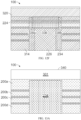
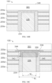
- the serial scribes 202 can comprise a first isolation scribe 212 (also referred to as a P1 scribe), a series connecting scribe 214 (also referred to as a P2 scribe), and a second isolation scribe 216 (also referred to as a P3 scribe).
- the first isolation scribe 212 can be formed to ensure that the TCO layer 140 is electrically isolated between cells 200.
- the first isolation scribe 212 can be formed though the TCO layer 140, the buffer layer 150, and the absorber layer 160 of photovoltaic device 100, or though the TCO layer 140, the buffer layer 150, the window layer 170, and the absorber layer 160 of the photovoltaic device 210.
- the first isolation scribe 212 bounding the reverse operation cell 208 can be filled with a dielectric material 198.
- the series connecting scribe 214 can be formed to electrically connect photovoltaic cells 200 in series.
- the series connecting scribe 214 can be utilized to provide a conductive path from the conductive layer 190 of one of the photovoltaic cells 200 to the TCO layer 140 of another of the photovoltaic cells 200.
- the series connecting scribe 214 can be formed through the absorber layer 160, and the back contact layer 180 of photovoltaic device 100, or through the window layer 170, the absorber layer 160, and the back contact layer 180 of the photovoltaic device 210.
- the series connecting scribe 214 can be formed through some or all of the buffer layer 150.
- the second isolation scribe 216 can be formed to isolate the back contact 190 into individual cells 200.
- the second isolation scribe 216 can be formed through the conductive layer 190, the back contact layer 180, and at least a portion of the absorber layer 160.
- the second isolation scribe 216 can be filled with a dielectric material 218.
- a parallel scribe 204 (also referred to as a P4 scribe) can be formed to isolate groups 206 of cells 200 from one another.
- each group 206 can comprise multiple photovoltaic cells 200 connected in series such as, for example, via the series connecting scribe 214.
- the parallel scribe 204 can be formed through the conductive layer 190, the back contact layer 180, the absorber layer 160, the buffer layer 150, the TCO layer 140, the barrier layer 130, and the window layer 170 (when present).
- each of the parallel scribe 204, the first isolation scribe 212, the series connecting scribe 214, and the second isolation scribe 216 can be formed via laser cutting or laser scribing.
- the parallel scribe 204 can be filled with a dielectric material.
- a plurality of photovoltaic cells 200 is formed on a substrate 110, where each of the photovoltaic cells 200 includes an absorber layer 160 and a conducting layer 190, the conducting layer 190 having a first surface 192 and a second surface 194, the first surface 192 of the conducting layer 190 facing the absorber layer 160.
- a bus member 224 is electrically coupled to the second surface 194 of the conducting layer 190 of at least one of the plurality of photovoltaic cells 200, where the bus member 224 is operable to collect current generated by the plurality of photovoltaic cells 200.
- a conductive member 226 is provided that has a portion 228 thereof adjacent a portion 230 of the bus member 224 to define a connection region 232 therebetween.
- the conductive member 226 extends from the connection region 232 over a portion of the plurality of photovoltaic cells 200.
- An insulating material 234 electrically insulates the conductive member 226 from the second surface 194 of the conducting layer 190 of the portion of the plurality of photovoltaic cells 200.
- An electrically conductive adhesive layer is disposed between the bus member 224 and the conductive member 226 within the connection region 232. Direct contact is made between the bus member 224 and the conductive member 226 through the electrically conductive adhesive layer within the connection region 232.
- the substrate 110 and the back support 196 may be laminated together so as to encapsulate the photovoltaic cells 200.
- the substrate 110 has a width and a length and the back support 196 may have substantially the same width and length as the substrate 110.
- Each of the substrate 110 and the back support 196 can include any suitable protective material such as, for example, borosilicate glass, float glass, soda lime glass, carbon fiber, or polycarbonate.
- FIG. 8 shows a perspective view of the back side of an example of a completed module.
- the module assembly 400 may include the layers described and depicted in FIGS. 1-5 , as well as bussing, encapsulation, and electrical connectors.
- the photovoltaic module assembly 400 may be configured to connect to a load through electrical connectors which pass through the junction box 440.
- the electrical connectors may include a first cable 415 with a first terminal 410, and a second cable 425 with a second terminal 420.
- the module assembly 400 may further include a supporting frame, bracket, or mount 430.
- the bussing may be added in a variety of manners and configurations.
- the bus members 224 can be metallic strips that may be added to the front and back sides of the photovoltaic device 100 to conduct direct current generated by the photovoltaic cells 200.
- two bus members 224 may be added to the photovoaic device 100, as described below and depicted in FIG. 6 , to conduct direct current generated by the photovoltaic cells 200.
- Bus members 224 may also be referred to as busbars, bus conductors, common conductors, photovoltaic ribbon, or buses.
- Each bus member 224 can function as one of a common positive and negative conductor, electrically connected to the first cells 200 in a series or the last cells 200 in a series, for example.
- FIGS. 9-14 depict one peripheral edge 340 and one set of bus member 224 and conductive member 226 which may be replicated on an opposing side of the photovoltaic device 100.
- FIGS. 9-14 depict one set of bussing components which may be replicated on an opposing side of the photovoltaic device 100.
- the first photovoltaic cell 200a may alternatively be the last photovoltaic cell.
- the insulating material 234 may be, for example, a double sided tape. However, other electrically insulating materials are possible.
- the insulating material 234 may electrically insulate the conductive member 226 from the second surface 194 of the conducting layer 190 of the photovoltaic cells 200 that the insulating material 234 touches, and may also hold the conductive member 226 in place.
- the conductive member 226 may be added over the insulating material 234, such that the conductive member 226 is not in direct contact with the photovoltaic cells 200. Rather, the conductive member 226 may be in direct contact with the insulating material 234. In this manner, the insulating material 234 may electrically insulate the conductive member 226 from the photovoltaic cells 200.
- the conductive member 226 may be any conductive material such as, but not limited to, a metal.
- the overlap of the bus member 224 over the conductive member 226 forms the configuration known as a T-joint 312.
- the bus member 224 may cross over the conductive member 226 in a substantially orthogonal manner. However, it is not necessary that the overlap of the bus member 224 over the conductive member 226 be substantially orthogonal.
- an edge seal 320 may be added over a portion of the photovoltaic device 100, after adding the bus member 224.
- the edge seal 320 may extend along the length Y from a location near a dead area at the first side edge 306 to a location near a dead area at the second side edge 308, and may be at or near the peripheral edge 340 of the photovoltaic device 100.
- the edge seal 320 may cover a portion of the first photovoltaic cell 200a. A portion of the dead area 301 may remain between the edge seal 320 and the peripheral edge 340 of the photovoltaic device 100.
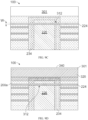
- the edge seal 320 extends to the peripheral edge 340 such that there is no dead area 301 uncovered by the edge seal 320. In the embodiment depicted in FIG. 9D , the edge seal 320 does not cover the bus member 224. Thus, in this embodiment, the edge seal 320 does not cover the T-joint 312.
- the edge seal 320 may protect the photovoltaic device 100 from moisture intrusion, foreign substances, and other environmental hazards.
- the edge seal 320 can also serve as an adhesive that bonds the device 100 together.
- Polyisobutylene (PIB) also known as butyl rubber, is a possible sealant material for the edge seal 320, though other examples of edge seal materials include, but are not limited to, opaque polymeric compounds.
- the edge seal material may also be dyed any desired color, and may contain any colorant.
- the edge seal material that forms the edge seal 320 may be applied in liquid hot melt form, in tape form, or by any other known technology. The liquid hot melt edge seal material may cool to a solid state when the susbtrate 110 and the back support 196 are combined during manufacturing.
- an interlayer 314 may be added to the photovoltaic device 100.
- the interlayer 314 may extend along the length Y from a location near a dead area at the first side edge 306 to a location near a dead area at the second side edge 308 of the photovoltaic device 100.
- the interlayer 314 may be applied to extend over a portion of the first photovoltaic cell 200a, and may completely cover the bus member 224 from a location near a dead area at the first side edge 306 to a location near a dead area at the second side edge 308. In this manner, the bus member 224 is protected by the interlayer 314 during subsequent manufacturing processes, and is therefore less susceptible to being moved from the forces involved in subsequent manfuacturing steps. Portions of the first photovoltaic cell 200a, the insulating member 234, and the conductive member 226 may remain uncovered by both the interlayer 314 and the edge seal 320.
- the interlayer 314 may serve multiple functions. First, the interlayer 314 may serve as a moisture barrier between the back support 196 and the plurality of photovoltaic cells 200. By being a moisture barrier, the interlayer 314 may prevent moisture-induced corrosion from occurring inside the photovoltaic device 100. This, in turn, may increase the device's life expectancy. Second, the interlayer 314 may serve as an electrical insulator between the electrically conductive core of the photovoltaic device 100 and any accessible points exterior to the photovoltaic device 100. For example, the interlayer 314 may limit or prevent leakage current from passing from the back contact through the back support 196 of the photovoltaic device 100.
- the interlayer 314 may serve as a bonding agent that attaches the back support 196 to the rest of the photovoltaic device 100.
- a lamination process may heat the interlayer 314 under vacuum to allow the material to wet-out any adjacent adherent surfaces, and in some cases initiate a cross-linking reaction. This process may promote bonding between the interlayer 314 and the back support 196 as well as between the interlayer 314 and the conducting layer 190.
- the interlayer 314, therefore, may serve as a bonding agent within the photovoltaic device 100.
- the interlayer 314 may include any suitable materials such as, for example, ethylene (EVA), polyvinyl butyral (PVB), polydimethylsiloxane (PDMS), polyiso-butylene (PIB), polyolefin, thermoplasatic polyurethane (TPU), polyurethane, epoxy, silicone, ionomer, or a combination thereof.
- EVA ethylene
- PVB polyvinyl butyral
- PDMS polydimethylsiloxane
- PIB polyiso-butylene
- TPU thermoplasatic polyurethane
- the interlayer 314 may include a base material and a filler material.
- the base material may be any of ethylene (EVA), polyvinyl butyral (PVB), polydimethylsiloxane (PDMS), polyiso-butylene (PIB), polyolefin, thermoplasatic polyurethane (TPU), polyurethane, epoxy, silicone, ionomer, or a combination thereof.
- the filler material can contain a flame retardant material, a dessicant material, a pigment, an inert material, or any combination thereof.
- the photovoltaic device depicted in FIGS. 9A-9E may include a first photovoltaic cell 200a that is larger in size than the neighboring photovoltaic cells 200b, 200c, 200d.
- the first photovoltaic cell 200a may extend for a distance di that is larger than each of the distance d 2 that the second photovoltaic cell 200b extends, the distance d 3 that the third photovoltaic cell 200c extends, and the distance d 4 that the fourth photovoltaic cell 200d extends. This allows for covering of the bus member 224 with the interlayer 314 without sacrificing edge seal width that is important to prevent moisture ingress from the environment.
- the interlayer 314 and the edge seal 320 may run on top of each other during the manufacturing process unless the edge seal 320 width is reduced, both of which would reduce the effectiveness of the edge seal 320 as a moisture barrier.
- the interlayer 314 would be deposited over a larger area of the photovoltaic device 100 - and therefore require a greater amount of interlayer material - in order to reach and cover the bus member 224, which extends over and is electrically coupled to the first photovoltaic cell 200a so as to collect the current generated from all of the photovoltaic cells 200 connected in series.
- the interlayer 314 may cover the bus member 224, and may cover a portion of the first photovoltaic cell 200a to do so.
- the interlayer 314 may protect the bus member 224 during subsequent manufacturing steps, during which the bus member 224 may otherwise become physically dislodged.
- the photovoltaic cells 200 are connected in series, the larger cell size of the first photovoltaic cell 200a does not result in a greater electric current being passed through the photovoltaic cells 200 to the bus member 224. Therefore, improved device efficiency can be achieved with bussing configurations that reduce the size of the first photovoltaic cell 200a while still protecting the bus member 224.
- Provided herein are photovoltaic devices having bussing configurations that provide for a reduction of the first photovoltaic cell size, and therefore realize higher device efficiency, while still protecting the bus member 224 during manfucturing.
- a photovoltaic device 100 at certain sequential steps of a manufacturing process is depicted.
- a dead area 301 abutting the peripheral edge 340 of the photovoltaic device 100 may be created by a suitable ablation method.
- the photovoltaic device 100 may include a first photovoltaic cell 200a adjacent to the dead area 301, a second photovoltaic cell 200b, a third photovoltaic cell 200c, and a fourth photovoltaic cell 200d, separated by the serial scribes 202. It is understood that four photovoltaic cells 200 are depicted for illustration purposes, but the number of photovoltaic cells 200 is not particularly limited.
- the first photovoltaic cell 200a has a smaller size compared to in the embodiment depicted in FIGS. 9A-9E .
- the distance d 1 that the first photovoltaic cell 200a extends may still be larger than each of the distances d 2 , d 3 , d 4 that the neighboring photovoltaic cells 200d, 200c, 200d extend, but the distance di that the first photovoltaic cell 200a extends may be smaller than the distance di that the first photovoltaic cell 200a extends in the embodiment depicted in FIGS. 9A-9E .
- the insulating material 234 may be added over the photovoltaic cells 200 in the same manner as previously described.
- the insulating material 234 may cover any number of the photovoltaic cells 200, provided that the insulating material 234 extends over at least a portion of the first photovoltaic cell 200a. It is not necessary that the insulating material 234 extend to the dead area 301, though the insulating material 234 may extend to the dead area 301.
- the conductive member 226 may be deposited on the insulating material 234.
- the conductive member 226 may not be in direct contact with the photovoltaic cells 200, but may be in direct contact with the insulating material 234.
- the insulating material 234 may serve to electrically insulate the conductive member 226 from the second surface 194 of the conducting layer 190 of the photovoltaic cells 200.
- the insulating material 234 may also hold the conductive member 226 in place during subsequent manufacturing steps.
- the bus member 224 may be added over the conductive member 226, insulating material 234, and the first photovoltaic cell 200a.
- the bus member 244 may extend along the length Y from a location near a dead area at the first side edge 306 of the photovoltaic device 100 to a location near a dead area at the second side edge 308 of the photovoltaic device 100.
- the bus member 224 may have a width W that extends in its entirety over the conductive member 226, and over the first photovoltaic cell 200a.
- the T-joint 312 is formed by the bus member 224 overlapping the conductive member 226, which may be in a substantially orthogonal manner (thus resembling a "T" shape). However, it is not necessary that the extension of the bus member 224 over the conductive member 226 be substantially orthogonal.
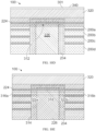
- the edge seal 320 may be added over the dead area 301 and the T-joint 312 from a location near a dead area at the first side edge 306 to a location near a dead area at the second side edge 308, so as to completely cover the T-joint 312. It is not necessary that the edge seal 320 extend all the way to the peripheral edge 340. Rather, some portion of the dead area 301 may remain uncovered by the edge seal 320. However, in some embodiments, the edge seal 320 may extend all the way to the peripheral edge 340, leaving no dead area 301 uncovered by the edge seal 320.
- the edge seal 320 fully covers the bus member 224 during subsequent manufacturing steps (such as a lamination process), thereby protecting the bus member 224 during subsequent manufacturing steps.
- the interlayer 314 may be added over the photovoltaic cells 200b, 200c, 200d, and a portion of the first photovoltaic cell 200a.
- a region 318 of the conductive member 226 and two regions 322a, 322b of the insulating material 234 may remain uncovered by the edge seal 320 and uncovered by the interlayer 314.
- the interlayer 314 is not used to cover the bus member 224 because the edge seal 320 covers the bus member 224. Accordingly, less interlayer material may be used than if the interlayer 314 were to cover the bus member 224.
- the bus member 224 may be deposited over the conductive member 226 and the insulating material 234 in an area closer to the peripheral edge 340 of the photovoltaic device 100 than in the embodiment depicted in FIGS. 9A-9E .
- the bus member 224 (and the T-joint 312) are wholly covered by the edge seal 320 instead of the interlayer 314, and therefore the amount of interlayer material needed to cover the bus member 224 is not a factor for determining the positioning of the bus member 224. Consequently, the first photovoltaic cell 200a may be made smaller than in the embodiment depicted in FIGS.
- the distance d 1 that the first photovoltaic cell 200a extends may be reduced so as to be closer in size to the distance d 2 that the second photovoltaic cell 200b extends, or the distances that the neighboring photovoltaic cells 200c, 200d extend. In this manner, overall efficiency of the photovoltaic device 100 may be improved.
- FIGS. 11A-11E an alternative embodiment of a photovoltaic device 100 at certain sequential steps during a manufacturing process is depicted.
- the T-joint 312 is covered by the edge seal 320, but less edge seal material is used compared to the embodiment depicted in FIGS. 10A-10E .
- the insulating material 234 may be added over the photovoltaic cells 200 in the same manner as before, extending over at least a portion of the first photovoltaic cell 200a.
- a dead area 301 may be created by a suitable ablation method adjacent to the peripheral edge 340 of the photovoltaic device 100.
- the dead area 301 may extend along the length Y from the first side edge 306 to the second side edge 308.
- the first photovoltaic cell 200a is adjacent to the dead area 301.
- the conductive member 226 may be added over the insulating material 234 as previously described.
- the conductive member 226 may be positioned over at least a portion of the first photovoltaic cell 200a.
- the conductive member 226 may extend over a plurality of the photovoltaic cells 200.
- the conductive member 226 may contact the dead area 301. In other embodiments, the conductive member 226 and the dead area 301 do not contact one another.
- the bus member 224 may be added over the conductive member 226 to form a T-joint 312 where the bus member 224 overlaps the conductive member 226.
- the bus member 224 may extend from a location near a dead area at the first side edge 306 to a location near a dead area at the second side edge 308 of the photovoltaic device 100.
- the bus member 224 may have a width W that extends in its entirety over the conductive member 226, and over the first photovoltaic cell 200a.
- the bus member 224 may be electrically coupled to the first photovotlaic cell 200a, and electrically coupled to the conductive member 226.
- the bus member 224 may be in direct contact with the first photovoltaic cell 200a, or may alternatively be electrically coupled thereto through a conductive metal or a conductive adhesive.
- the bus member 224 may be in direct contact with the conductive member 226, or may alternatively be electrically coupled thereto through a conductive adhesive.
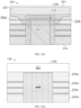
- the edge seal 320 may be formed in a shape that includes a tab 324 extending over the T-joint 312.
- the edge seal 320 may be disposed along or near the peripheral edge 340, but need not extend all the way to the peripheral edge 340. Rather, as seen in FIG. 11D , some of the dead area 301 may remain uncovered by the edge seal 340.
- Some of the edge seal 320 may extend along the length Y from a location near a dead area at the first side edge 306 to a location near a dead area at the second side edge 308, while the tab 324 does not extend along then length Y to the same extent.
- the tab 324 may have a shorter length l 2 compared to the length l 1 of the remaining edge seal 320.
- the edge seal 320 may include side portions 360, 362 which extend from the region 321 of the edge seal 320 having the longer length l 1 to the tab 324 having the shorter length l 2 .
- the side portions 360, 362 may be angular, as seen in FIG. 11D , or may alternatively be substantially parallel to the first side edge 306 and the second side edge 308.
- the edge seal 320 is defined by a region 321 having a first length l 1 from the first side edge 320 to the side portion 360 which extends inwardly from the peripheral edge 340 to the serial scribe line 202, and then the tab 324 having a second length l 2 from the side portion 360 over the T-joint 312 to the side portion 362, which extends back to the region 321 having the first length l 1 .
- the edge seal 320 may have the first length l 1 over the dead area 301, and the second length l 2 over the T-joint 312, where the first length l 1 is greater than the second length l 2 .
- this embodiment does not require as much material to form the edge seal 320 as the embodiment depicted in FIGS. 10A-10E .
- This embodiment also allows for a reduced size of the first photovoltaic cell 200a, because the interlayer 314 is not used to cover and protect the T-joint 312.
- FIGS. 12A-12F an alternative embodiment of a photovoltaic device 100 at certain sequential steps of a manufacturing process is depicted.
- the insulating material 234 may be added over the photovoltaic cells 200, and the conductive member 226 may be added over the insulating material 234, as previously described.
- a dead area 301 may extend inwardly from the peripheral edge 340 of the photovoltaic device 100, formed by a suitable ablation method.
- the insulating material 234 has a peripheral edge 334 that may be over the first photovoltaic cell 200a, and may be near the dead area 301. In other embodiments, the peripheral edge 334 of the insulating material 234 may be on the dead area 301.
- the conductive member 226 has a peripheral edge 358 that may be on the opposite side of the peripheral edge 334 from the dead area 301, though still over the first photovoltaic cell 200a.
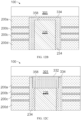
- a bridge 332 may be formed over the insulating material 234 and the conductive member 226.
- the bridge 332 may cover the peripheral edge 358 of the conductive member 226, and may extend over adjacent portions of the insulating material 234.
- the bridge 332 may extend over the peripheral edge 334 of the insulating material 234.
- the bridge 332 can be formed, for example, from a wide conductive metal with conductive adhesive and can serve to bridge the bus member 224 and the conductive member 226.
- the bridge 332 is a multilayer structure composed of one or more conductive metal layers and one or more conductive adhesive layers.
- the bridge 332 is a multilayer structure composed of a liner, one or more layers of a conductive metal, and one or more layers of a conductive adhesive. In some embodiments, the bridge 332 is a multilayer structure composed of two or more conductive metal layers and two or more conductive adhesive layers.
- the bus member 224 may be added over the bridge 332.
- the bus member 224 may extend along the length Y from a location near a dead area at the first side edge 306 to a location near a dead area at the second side edge 308 of the photovoltaic device 100.
- the bus member 224 may have a width Wthat is completely over the first photovoltaic cell 200a.
- the bus member 224 may be electrically coupled to the first photovoltaic cell 200a, for example, by directly contacting the first photovoltaic cell 200a or through a conductive metal or a conductive adhesive. Additionally, the bus member 224 may be in direct contact with the bridge 332.
- the bridge 332 may be disposed between the conductive member 226 and the bus member 224.
- the bridge 332 may be configured to electrically couple the conductive member 226 to the bus member 224.
- the bridge 332 may serve to enhance the conduction of current between the bus member 224 and the conductive member 226.
- the bridge 332 is a multilayer structure composed of two or more conductive metal layers and two or more conductive adhesive layers. In contrast to the previous embodiment, however, the bridge 332 may be disposed on top of the bus member 224 and the conductive member 226 such that a portion of the bus member 224 is disposed between the insulating material 234 and the bridge 332, and a portion of the conductive member 226 is disposed between the insulating material 234 and the bridge 332.
- the bus member 224 may not be in direct contact with the conductive member 226, but is electrically coupled to the conductive member 226 through the bridge 332.
- the bus member 224 is conductive on both sides to facilitate electrical communication. That is, the bus member 224 may include a first surface facing the first photovoltaic cell 200a comprising a conductive material, and a second surface facing the bridge 332 comprising a conductive material.
- the edge seal 320 may extend along the length Y from a location near a dead area at the first side edge 306 to a location near a dead area at the second side edge 308, leaving uncovered some of the dead area 301 adjacent the peripheral edge 340 of the photovoltaic device 100.
- the edge seal 320 may extend to the peripheral edge 340 such that none of the dead area 301 remains uncovered by the edge seal 320.
- the edge seal 320 may extend along the width X so as to cover the exposed portions of the bus member 224 not covered by the bridge 332.
- the bridge 332 and the edge seal 320 may protect the bus member 224 during subsequent manufacturing steps.
- the edge seal 320 and the interlayer 314 may be added as previously described, extending along the length Y from a location near a dead area at the first side edge 306 to a location near a dead area at the second side edge 308 of the photovoltaic device 100.
- the edge seal 320 may completely cover the bus member 224, and therefore protect the bus member 224 during subsequent manufacturing steps. Areas 348a, 348b of the insulating material 234 on respective sides of the patch 342, and an area 351 of the patch 342, may remain uncovered by the edge seal 320 and uncovered by the interlayer 314. However, the bus member 224 may be completely covered by the edge seal 320.
- a photovoltaic device may include a bridge composed of a conductive metal and a conductive adhesive that electrically couples a bus member to a conductive member.
- the bridge may be a multilayer structure composed of two or more layers of the conductive metal and two or more layers of the conductive adhesive.
- the bridge may be a multilayer structure composed of one or more conductive metal layers and one or more conductive adhesive layers.
- the bridge may be a multilayer structure composed of a liner, one or more layers of a conductive metal, and one or more layers of a conductive adhesive.
- a photovoltaic device having a bridge or a patch as described herein may also have a bus member that is not fully covered by an edge seal. Rather, the bus member may include one or more portions that are not disposed between the edge seal and the photovoltaic cells.
- a photovoltaic device may include an edge seal having a first length over a dead area, and a second length over a T-joint defined by the overlap of a bus member over a conductive member, where the first length is greater than the second length.
- the bus member of such a photovoltaic device comprises two portions that are uncovered by the edge seal.
- the photovoltaic device further comprises a bridge as described herein.
- the photovoltaic device further comprises a patch as described herein.
Landscapes
- Photovoltaic Devices (AREA)
Abstract
Description
- A photovoltaic device generates electrical power by converting light into electricity using semiconductor materials that exhibit the photovoltaic effect. Photovoltaic devices include a number of layers divided into a plurality of photovoltaic cells. Each photovoltaic cell can convert a light source, such as sunlight, into electrical power and can be connected in series with one or more adjacent cells. Accordingly, current generated by adjacent cells can flow through each of the photovoltaic cells.
- Improving contact between current collection portions of the photovoltaic device is important for efficient and durable operation of the device. For example, the electrical junction between the conductive member and bus member is a current collection contact that is important for maintaining function of the photovoltaic device. If the junction is compromised or fails, an open circuit can be created and the photovoltaic device will be rendered inoperable. Accordingly, there exists an ongoing need in the industry for an improved, more robust, and more reliable electrical contact between the conductive member and bus member that can increase the performance of photovoltaic devices.
-
-
FIG. 1 schematically depicts a photovoltaic device according to one or more embodiments shown and described herein; -
FIG. 2 schematically depicts a cross-sectional view along 2-2 of the photovoltaic device ofFIG. 1 according to one or more embodiments shown and described herein; -
FIG. 3 schematically depicts a substrate according to one or more embodiments shown and described herein; -
FIG. 4 schematically depicts a photovoltaic device according to one or more embodiments shown and described herein; -
FIG. 5 schematically depicts a cross-sectional view along 5-5 of the photovoltaic device ofFIG. 1 according to one or more embodiments shown and described herein; -
FIG. 6 schematically depicts a photovoltaic device according to one or more embodiments shown and described herein. -
FIG. 7 schematically depicts a T-joint shaped contact between current collection portions the photovoltaic device according to one or more embodiments shown and described herein, showing a view along 7-7 of the photovoltaic device ofFIG. 6 ; -
FIG. 8 schematically depicts a back view of a photovoltaic device; -
FIGS. 9A-9E schematically depict a photovoltaic device according to one or more embodiments shown and described herein during sequential steps of a manufacturing process; -
FIGS. 10A-10E schematically depict a photovoltaic device according to one or more embodiments shown and described herein during sequential steps of a manufacturing process; -
FIGS. 11A-11E schematically depict a photovoltaic device according to one or more embodiments shown and described herein during sequential steps of a manufacturing process; -
FIGS. 12A-12F schematically depict a photovoltaic device according to one or more embodiments shown and described herein during sequential steps of a manufacturing process; -
FIGS. 13A-13F schematically depict a photovoltaic device according to one or more embodiments shown and described herein during sequential steps of a manufacturing process; and -
FIGS. 14A-14E schematically depict a photovoltaic device according to one or more embodiments shown and described herein during sequential steps of a manufacturing process. - Photovoltaic devices can be formed by deposition of various semiconductor materials and electrode layers as thin (generally recognized in the art as less than 10 microns) film layers on a glass substrate. The substrate can then undergo various processing steps, including laser scribing processes, to define and isolate individual photovoltaic cells, define a perimeter edge zone around the photovoltaic cells, and to connect the photovoltaic cells in series. These steps can result in generation of a plurality of individual photovoltaic cells defined within the physical edges of the substrate.
- One method for collecting the current from a photovoltaic device is to attach an insulating material (e.g., an insulating tape) lengthwise along the device across the photovoltaic cells. A conductive member (e.g., a conductive foil tape or ribbon) can then be aligned and attached to the insulating material. A bus member (e.g., a bus bar in the form of an adhesive bus tape) can then be attached at opposite longitudinal ends of the device, aligned with the first and last cells, respectively. The bus member can cross over and attach to the conductive member, collect the current from the cells, and transfer the current to the conductive member. The conductive member can be separated in a junction box where leads are connected to separated ends of the conductive member. The leads can provide a means to connect the photovoltaic device to a load, other cells, a grid, and so forth.
- The present technology improves reliability and durability of current collecting portions of photovoltaic devices to improve performance of photovoltaic devices. For example, the current from a photovoltaic device can be collected by attaching an insulating material (e.g., an insulating tape) lengthwise along the device across the photovoltaic cells and aligning and attaching a conductive member (e.g., a conductive foil tape or ribbon) to the insulating material. A bus member (e.g., a bus bar in the form of an adhesive bus tape) can then be attached at opposite longitudinal ends of the photovoltaic device, aligned with the first and last cells of the photovoltaic device, respectively. In certain configurations, the bus member can cross over and attach to the conductive member, collect the current from the cells, and transfer the current to the conductive member. Where the bus member crosses over near an end of the conductive member, the connection can be described as a T-shaped junction or a T-joint. The T-joint is where the current from the photovoltaic device can accumulate, thus a low and stable contact resistance at that location can be important to maintain good device performance. However, it is possible that during various manufacturing steps, a bus member may be physically displaced by the forces involved in manufacturing, and so it is advantageous to protect the bus member during manufacturing.
- Referring now to
FIG. 1 , an embodiment of aphotovoltaic device 100 is schematically depicted. Thephotovoltaic device 100 can be configured to receive light and transform light into electrical signals, e.g., photons can be absorbed from the light and transformed into electrical signals via the photovoltaic effect. Accordingly, thephotovoltaic device 100 can define anenergy side 102 configured to be exposed to a light source such as, for example, the sun. Thephotovoltaic device 100 can also define anopposing side 104 offset from theenergy side 102 such as, for example, by a plurality of material layers. It is noted that the term "light" can refer to various wavelengths of the electromagnetic spectrum such as, but not limited to, wavelengths in the ultraviolet (UV), infrared (IR), and visible portions of the electromagnetic spectrum. "Sunlight," as used herein, refers to light emitted by the sun. - The
photovoltaic device 100 can include a plurality of layers disposed between theenergy side 102 and theopposing side 104. As used herein, the term "layer" refers to a thickness of material provided upon a surface. Each layer can cover all or any portion of the surface. In some embodiments, the layers of thephotovoltaic device 100 can be divided into an array ofphotovoltaic cells 200. For example, thephotovoltaic device 100 can be scribed according to a plurality ofserial scribes 202 and a plurality ofparallel scribes 204. Theserial scribes 202 can extend along a length Y of thephotovoltaic device 100 and demarcate thephotovoltaic cells 200 along the length Y of thephotovoltaic device 100. Theserial scribes 202 can be configured to connect neighboring cells of thephotovoltaic cells 200 serially along a width X of thephotovoltaic device 100.Serial scribes 202 can form a monolithic interconnect of the neighboring cells, i.e., adjacent to theserial scribe 202. Theparallel scribes 204 can extend along the width X of thephotovoltaic device 100 and demarcate thephotovoltaic cells 200 along the width X of thephotovoltaic device 100. Under operations, current 205 can predominantly flow along the width X through thephotovoltaic cells 200 serially connected by theserial scribes 202. Under operations,parallel scribes 204 can limit the ability of current 205 to flow along the length Y.Parallel scribes 204 are optional and can be configured to separate thephotovoltaic cells 200 that are connected serially into groups 206 arranged along length Y. Accordingly, theserial scribes 202 and theparallel scribes 204 can demarcate the array of thephotovoltaic cells 200. - Referring still to
FIG. 1 , theparallel scribes 204 can electrically isolate the groups 206 ofphotovoltaic cells 200 that are connected serially. In some embodiments, the groups 206 of thephotovoltaic cells 200 can be connected in parallel such as, for example, via electrical bussing. Optionally, the number ofparallel scribes 204 can be configured to limit a maximum current generated by each group 206 of thephotovoltaic cells 200. In some embodiments, the maximum current generated by each group 206 can be less than or equal to about 200 milliamps (mA) such as, for example, less than or equal to about 100 mA in one embodiment, less than or equal to about 75 mA in another embodiment, or less than or equal to about 50 mA in a further embodiment. - Referring collectively to
FIGS. 1 and2 , the layers of thephotovoltaic device 100 can include asubstrate 110 configured to facilitate the transmission of light into thephotovoltaic device 100. Thesubstrate 110 can be disposed at theenergy side 102 of thephotovoltaic device 100. Referring now toFIGS. 2 and 3 , thesubstrate 110 can have afirst surface 112 substantially facing theenergy side 102 of thephotovoltaic device 100 and asecond surface 114 substantially facing the opposingside 104 of thephotovoltaic device 100. One or more layers of material can be disposed between thefirst surface 112 and thesecond surface 114 of thesubstrate 110. - The
substrate 110 can include atransparent layer 120 having afirst surface 122 substantially facing theenergy side 102 of thephotovoltaic device 100 and asecond surface 124 substantially facing the opposingside 104 of thephotovoltaic device 100. In some embodiments, thesecond surface 124 of thetransparent layer 120 can form thesecond surface 114 of thesubstrate 110. Thetransparent layer 120 can be formed from a substantially transparent material such as, for example, glass. Suitable glass can include soda-lime glass, or any glass with reduced iron content. Thetransparent layer 120 can have any suitable transmittance, including about 250 nm to about 1,300 nm in some embodiments, or about 250 nm to about 950 nm in other embodiments. Thetransparent layer 120 may also have any suitable transmission percentage, including, for example, more than about 50% in one embodiment, more than about 60% in another embodiment, more than about 70% in yet another embodiment, more than about 80% in a further embodiment, or more than about 85% in still a further embodiment. In one embodiment,transparent layer 120 can be formed from a glass with about 90% transmittance, or more. Optionally, thesubstrate 110 can include acoating 126 applied to thefirst surface 122 of thetransparent layer 120. Thecoating 126 can be configured to interact with light or to improve durability of thesubstrate 110 such as, but not limited to, an antireflective coating, an antisoiling coating, or a combination thereof. - Referring again to
FIG. 2 , thephotovoltaic device 100 can include abarrier layer 130 configured to mitigate diffusion of contaminants (e.g., sodium) from thesubstrate 110, which could result in degradation or delamination. Thebarrier layer 130 can have afirst surface 132 substantially facing theenergy side 102 of thephotovoltaic device 100 and asecond surface 134 substantially facing the opposingside 104 of thephotovoltaic device 100. In some embodiments, thebarrier layer 130 can be provided adjacent to thesubstrate 110. For example, thefirst surface 132 of thebarrier layer 130 can be provided upon thesecond surface 114 of thesubstrate 100. The phrase "adjacent to," as used herein, means that two layers are disposed contiguously and without any intervening materials between at least a portion of the layers. - Generally, the
barrier layer 130 can be substantially transparent, thermally stable, with a reduced number of pin holes and having high sodium-blocking capability, and good adhesive properties. Alternatively or additionally, thebarrier layer 130 can be configured to apply color suppression to light. Thebarrier layer 130 can include one or more layers of suitable material, including, but not limited to, tin oxide, silicon dioxide, aluminum-doped silicon oxide, silicon oxide, silicon nitride, or aluminum oxide. Thebarrier layer 130 can have any suitable thickness bounded by thefirst surface 132 and thesecond surface 134, including, for example, more than about 100 Å in one embodiment, more than about 150 Å in another embodiment, or less than about 200 Å in a further embodiment. - Referring still to
FIG. 2 , thephotovoltaic device 100 can include a transparent conductive oxide (TCO)layer 140 configured to provide electrical contact to transport charge carriers generated by thephotovoltaic device 100. TheTCO layer 140 can have afirst surface 142 substantially facing theenergy side 102 of thephotovoltaic device 100 and asecond surface 144 substantially facing the opposingside 104 of thephotovoltaic device 100. In some embodiments, theTCO layer 140 can be provided adjacent to thebarrier layer 130. For example, thefirst surface 142 of theTCO layer 140 can be provided upon thesecond surface 134 of thebarrier layer 130. Generally, theTCO layer 140 can be formed from one or more layers of n-type semiconductor material that is substantially transparent and has a wide band gap. Specifically, the wide band gap can have a larger energy value compared to the energy of the photons of the light, which can mitigate undesired absorption of light. TheTCO layer 140 can include one or more layers of suitable material, including, but not limited to, tin dioxide, doped tin dioxide (e.g., F-SnO2), indium tin oxide, or cadmium stannate. - The
photovoltaic device 100 can include abuffer layer 150 configured to provide an insulating layer between theTCO layer 140 and any adjacent semiconductor layers. Thebuffer layer 150 can have afirst surface 152 substantially facing theenergy side 102 of thephotovoltaic device 100 and asecond surface 154 substantially facing the opposingside 104 of thephotovoltaic device 100. In some embodiments, thebuffer layer 150 can be provided adjacent to theTCO layer 140. For example, thefirst surface 152 of thebuffer layer 150 can be provided upon thesecond surface 144 of theTCO layer 140. Thebuffer layer 140 may include material having higher resistivity than the TCO later 140, including, but not limited to, intrinsic tin dioxide, zinc magnesium oxide (e.g., Zn1-xMgxO), silicon dioxide (SnO2), aluminum oxide (Al2O3), aluminum nitride (AlN), zinc tin oxide, zinc oxide, tin silicon oxide, or any combination thereof. In some embodiments, the material of thebuffer layer 140 can be configured to substantially match the band gap of an adjacent semiconductor layer (e.g., an absorber). Thebuffer layer 150 may have any suitable thickness between thefirst surface 152 and thesecond surface 154, including, for example, more than about 100 Å in one embodiment, between about 100 Å and about 800 Å in another embodiment, or between about 150 Å and about 600 Å in a further embodiment. - Referring still to
FIG. 2 , thephotovoltaic device 100 can include anabsorber layer 160 configured to cooperate with another layer and form a p-n junction within thephotovoltaic device 100. Accordingly, absorbed photons of the light can free electron-hole pairs and generate carrier flow, which can yield electrical power. Theabsorber layer 160 can have afirst surface 162 substantially facing theenergy side 102 of thephotovoltaic device 100 and asecond surface 164 substantially facing the opposingside 104 of thephotovoltaic device 100. A thickness of theabsorber layer 160 can be defined between thefirst surface 162 and thesecond surface 164. The thickness of theabsorber layer 160 can be between about 0.5 µm to about 10 µm such as, for example, between about 1 µm to about 7 µm in one embodiment, or between about 1.5 µm to about 4 µm in another embodiment. - According to the embodiments described herein, the
absorber layer 160 can be formed from a p-type semiconductor material having an excess of positive charge carriers, i.e., holes or acceptors. Theabsorber layer 160 can include any suitable p-type semiconductor material such as group II-VI semiconductors. Specific examples include, but are not limited to, semiconductor materials comprising cadmium, tellurium, selenium, or any combination thereof. Suitable examples include, but are not limited to, ternaries of cadmium, selenium and tellurium (e.g., CdSexTe1-x), or a compound comprising cadmium, selenium, tellurium, and one or more additional element. Theabsorber layer 160 may further comprise one or more dopants. Photovoltaic devices may include a plurality of absorber materials. - In embodiments where the
absorber layer 160 comprises tellurium and cadmium, the atomic percent of the tellurium can be greater than or equal to about 25 atomic percent and less than or equal to about 50 atomic percent such as, for example, greater than about 30 atomic percent and less than about 50 atomic percent in one embodiment, greater than about 40 atomic percent and less than about 50 atomic percent in a further embodiment, or greater than about 47 atomic percent and less than about 50 atomic percent in yet another embodiment. Alternatively or additionally, the atomic percent of the tellurium in theabsorber layer 160 can be greater than about 45 atomic percent such as, for example, greater than about 49% in one embodiment. It is noted that the atomic percent described herein is representative of the entirety of theabsorber layer 160, the atomic percentage of material at a particular location within theabsorber layer 160 can vary with thickness compared to the overall composition of theabsorber layer 160. - In embodiments where the
absorber layer 160 comprises selenium and tellurium, the atomic percent of the selenium in theabsorber layer 160 can be greater than about 0 atomic percent and less or equal to than about 25 atomic percent such as, for example, greater than about 1 atomic percent and less than about 20 atomic percent in one embodiment, greater than about 1 atomic percent and less than about 15 atomic percent in another embodiment, or greater than about 1 atomic percent and less than about 8 atomic percent in a further embodiment. It is noted that the concentration of tellurium, selenium, or both can vary through the thickness of theabsorber layer 160. For example, when theabsorber layer 160 comprises a compound including selenium at a mole fraction of x and tellurium at a mole fraction of 1-x (SexTe1-x), x can vary in theabsorber layer 160 with distance from thefirst surface 162 of theabsorber layer 160. - Referring still to
FIG. 2 , theabsorber layer 160 can be doped with a dopant configured to manipulate the charge carrier concentration. In some embodiments, theabsorber layer 160 can be doped with a Group I or V dopant such as, for example, copper, arsenic, phosphorous, antimony, or a combination thereof. The total density of the dopant within theabsorber layer 160 can be controlled. Alternatively or additionally, the amount of the dopant can vary with distance from thefirst surface 162 of theabsorber layer 160. In some embodiments, dopants are introduced during a passivation step in the manufacturing process. Passivation may include, for example, treatment with CdCl2 or other halide compounds, and resulting dopants may include chlorine or other halogens. Additionally, the amount of a selected dopant can vary with distance from thefirst surface 162 of theabsorber layer 160. - According to the embodiments provided herein, the p-n junction can be formed by providing the
absorber layer 160 sufficiently close to a portion of thephotovoltaic device 100 having an excess of negative charge carriers, i.e., electrons or donors. In some embodiments, theabsorber layer 160 can be provided adjacent to n-type semiconductor material. Alternatively, one or more intervening layers can be provided between theabsorber layer 160 and n-type semiconductor material. In some embodiments, theabsorber layer 160 can be provided adjacent to thebuffer layer 150. For example, thefirst surface 162 of theabsorber layer 160 can be provided upon thesecond surface 154 of thebuffer layer 150. - Referring now to
FIG. 4 , in some embodiments, aphotovoltaic device 210 can include a window layer 170 comprising n-type semiconductor material. Theabsorber layer 160 can be formed adjacent to the window layer 170. The window layer 170 can have afirst surface 172 substantially facing theenergy side 102 of thephotovoltaic device 100 and asecond surface 174 substantially facing the opposingside 104 of thephotovoltaic device 100. In some embodiments, the window layer 170 can be positioned between theabsorber layer 160 and the TCO layer 20. In one embodiment, the window layer 170 can be positioned between theabsorber layer 160 and thebuffer layer 150. The window layer 170 can include any suitable material, including, for example, cadmium sulfide, zinc sulfide, cadmium zinc sulfide, zinc magnesium oxide, or any combination thereof. The material of the window layer 170 can include dopants. - Referring collectively to
FIGS. 2 and4 , thephotovoltaic device back contact layer 180 configured to mitigate undesired alteration of the dopant and to provide electrical contact to theabsorber layer 160. Theback contact layer 180 can have afirst surface 182 substantially facing theenergy side 102 of thephotovoltaic device 100 and asecond surface 184 substantially facing the opposingside 104 of thephotovoltaic device 100. A thickness of theback contact layer 180 can be defined between thefirst surface 182 and thesecond surface 184. The thickness of theback contact layer 180 can be between about 5 nm to about 200 nm such as, for example, between about 10 nm to about 50 nm in one embodiment. - In some embodiments, the
back contact layer 180 can be provided adjacent to theabsorber layer 160. For example, thefirst surface 182 of theback contact layer 180 can be provided upon thesecond surface 164 of theabsorber layer 160. In some embodiments, theback contact layer 180 can include binary or ternary combinations of materials from Groups I, II, VI, such as for example, one or more layers containing zinc, copper, cadmium, and tellurium in various compositions. Further exemplary materials include, but are not limited to, zinc telluride doped with copper telluride, or zinc telluride alloyed with copper telluride. - The
photovoltaic device 100 can include aconducting layer 190 configured to provide electrical contact with theabsorber layer 160. Theconducting layer 190 can have afirst surface 192 substantially facing theenergy side 102 of thephotovoltaic device 100 and asecond surface 194 substantially facing the opposingside 104 of thephotovoltaic device 100. In some embodiments, theconducting layer 190 can be provided adjacent to theback contact layer 180. For example, thefirst surface 192 of theconducting layer 190 can be provided upon thesecond surface 184 of theback contact layer 180. Theconducting layer 190 can include any suitable conducting material such as, for example, one or more layers of nitrogen-containing metal, silver, nickel, copper, aluminum, titanium, palladium, chrome, molybdenum, gold, or the like. Suitable examples of a nitrogen-containing metal layer can include aluminum nitride, nickel nitride, titanium nitride, tungsten nitride, selenium nitride, tantalum nitride, or vanadium nitride. - The
photovoltaic device back support 196 configured to cooperate with thesubstrate 110 to form a housing for thephotovoltaic device 100. Theback support 196 can be disposed at the opposingside 102 of thephotovoltaic device 100. For example, theback support 196 can be formed adjacent to theconducting layer 190. Theback support 196 can include any suitable material, including, for example, glass (e.g., soda-lime glass). In some embodiments, an encapsulation layer can also function as theback support 196. - Referring collectively to
FIGS. 2 ,4, and 5 , manufacturing of aphotovoltaic device - Manufacturing of
photovoltaic devices photovoltaic cells 200. For example, theserial scribes 202 can comprise a first isolation scribe 212 (also referred to as a P1 scribe), a series connecting scribe 214 (also referred to as a P2 scribe), and a second isolation scribe 216 (also referred to as a P3 scribe). Thefirst isolation scribe 212 can be formed to ensure that theTCO layer 140 is electrically isolated betweencells 200. Specifically, thefirst isolation scribe 212 can be formed though theTCO layer 140, thebuffer layer 150, and theabsorber layer 160 ofphotovoltaic device 100, or though theTCO layer 140, thebuffer layer 150, the window layer 170, and theabsorber layer 160 of thephotovoltaic device 210. Thefirst isolation scribe 212 bounding thereverse operation cell 208 can be filled with adielectric material 198. - Referring again to
FIGS. 2 and4 , theseries connecting scribe 214 can be formed to electrically connectphotovoltaic cells 200 in series. For example, theseries connecting scribe 214 can be utilized to provide a conductive path from theconductive layer 190 of one of thephotovoltaic cells 200 to theTCO layer 140 of another of thephotovoltaic cells 200. Theseries connecting scribe 214 can be formed through theabsorber layer 160, and theback contact layer 180 ofphotovoltaic device 100, or through the window layer 170, theabsorber layer 160, and theback contact layer 180 of thephotovoltaic device 210. Optionally, theseries connecting scribe 214 can be formed through some or all of thebuffer layer 150. Accordingly, theseries connecting scribe 214 can be formed after theback contact layer 180 is deposited. Theseries connecting scribe 214 can then be filled with a conducting material such as, but not limited to, the material of theconducting layer 190. In some embodiments, the conductive material can be more conductive in reverse bias relative to forward bias. - The
second isolation scribe 216 can be formed to isolate theback contact 190 intoindividual cells 200. Thesecond isolation scribe 216 can be formed through theconductive layer 190, theback contact layer 180, and at least a portion of theabsorber layer 160. Thesecond isolation scribe 216 can be filled with adielectric material 218. - Referring collectively to
FIGS. 1 and5 , a parallel scribe 204 (also referred to as a P4 scribe) can be formed to isolate groups 206 ofcells 200 from one another. In some embodiments, each group 206 can comprise multiplephotovoltaic cells 200 connected in series such as, for example, via theseries connecting scribe 214. Theparallel scribe 204 can be formed through theconductive layer 190, theback contact layer 180, theabsorber layer 160, thebuffer layer 150, theTCO layer 140, thebarrier layer 130, and the window layer 170 (when present). According to the embodiments provided herein, each of theparallel scribe 204, thefirst isolation scribe 212, theseries connecting scribe 214, and thesecond isolation scribe 216 can be formed via laser cutting or laser scribing. In some embodiments, theparallel scribe 204 can be filled with a dielectric material. - With reference now to
FIGS. 5-7 , an embodiment of thephotovoltaic device photovoltaic cells 200 is formed on asubstrate 110, where each of thephotovoltaic cells 200 includes anabsorber layer 160 and aconducting layer 190, theconducting layer 190 having afirst surface 192 and asecond surface 194, thefirst surface 192 of theconducting layer 190 facing theabsorber layer 160. Abus member 224 is electrically coupled to thesecond surface 194 of theconducting layer 190 of at least one of the plurality ofphotovoltaic cells 200, where thebus member 224 is operable to collect current generated by the plurality ofphotovoltaic cells 200. Aconductive member 226 is provided that has aportion 228 thereof adjacent aportion 230 of thebus member 224 to define a connection region 232 therebetween. Theconductive member 226 extends from the connection region 232 over a portion of the plurality ofphotovoltaic cells 200. An insulatingmaterial 234 electrically insulates theconductive member 226 from thesecond surface 194 of theconducting layer 190 of the portion of the plurality ofphotovoltaic cells 200. An electrically conductive adhesive layer is disposed between thebus member 224 and theconductive member 226 within the connection region 232. Direct contact is made between thebus member 224 and theconductive member 226 through the electrically conductive adhesive layer within the connection region 232. - With reference again to
FIG. 7 , it can be seen that theportion 228 of theconductive member 226 adjacent theportion 230 of thebus member 224 that defines the connection region 232 therebetween is provided by having theportion 230 of thebus member 224 overlap theportion 228 of theconductive member 226. It can be further seen that thebus member 224 crosses over theconductive member 226 at the connection region 232. In this way, thebus member 224 can be electrically coupled to thesecond surface 194 of theconducting layer 190 of one or morephotovoltaic cells 200 on each side of theconductive member 226, where thebus member 224 is hence operable to collect current generated by thephotovoltaic cells 200 on each side of theconductive member 226. - After the layer stack with scribes is formed, bussing may be added as described above and in more detail below, and the photovoltaic device may be assembled. An encapsulation layer may be applied and the semiconductor layers may be sealed relative to rain, snow, and other metrological elements. Referring now to
FIG. 8 , thesubstrate 110 and theback support 196 may be laminated together so as to encapsulate thephotovoltaic cells 200. Thesubstrate 110 has a width and a length and theback support 196 may have substantially the same width and length as thesubstrate 110. Each of thesubstrate 110 and theback support 196 can include any suitable protective material such as, for example, borosilicate glass, float glass, soda lime glass, carbon fiber, or polycarbonate. Alternatively, theback support 196 may be any suitable material such as a polymer-based back sheet. Theback support 196 andsubstrate 110 can protect the various layers of thephotovoltaic device 100 from exposure to moisture and other environmental hazards.FIG. 8 shows a perspective view of the back side of an example of a completed module. The module assembly 400 may include the layers described and depicted inFIGS. 1-5 , as well as bussing, encapsulation, and electrical connectors. The photovoltaic module assembly 400 may be configured to connect to a load through electrical connectors which pass through thejunction box 440. The electrical connectors may include a first cable 415 with a first terminal 410, and a second cable 425 with asecond terminal 420. The module assembly 400 may further include a supporting frame, bracket, or mount 430. - Referring now to
FIGS. 5-7 and9-14 , the bussing may be added in a variety of manners and configurations. Thebus members 224 can be metallic strips that may be added to the front and back sides of thephotovoltaic device 100 to conduct direct current generated by thephotovoltaic cells 200. In general, twobus members 224 may be added to thephotovoaic device 100, as described below and depicted inFIG. 6 , to conduct direct current generated by thephotovoltaic cells 200.Bus members 224 may also be referred to as busbars, bus conductors, common conductors, photovoltaic ribbon, or buses. Eachbus member 224 can function as one of a common positive and negative conductor, electrically connected to thefirst cells 200 in a series or thelast cells 200 in a series, for example. - It is understood that although
FIGS. 9-14 depict bussing configurations near aperipheral edge 340, thephotovoltaic device 100 may have a second peripheral edge on an opposing side and a corresponding bussing configuration near the second peripheral edge. In such embodiments, thebus member 224 near theperipheral edge 340 may act as a positive bus, and a second bus member near the second peripheral edge may act as a negative bus. For example, referring now toFIG. 6 , aphotovoltaic device 100 may have a first peripheral edge 340a on a first side 207 with a first bus member 224a extending along the length Y and a first conductive member 226a extending along the width X, and a second peripheral edge 340b on an opposing second side 209 with a second bus member 224b extending along the length Y and a second conductive member 226b extending along the width X. Thephotovoltaic device 100 may have a first side edge 306 and asecond side edge 308 extending along the width X on opposing sides of the length Y, and each of the first side edge 306 andsecond side edge 308 may include a dead area similar to each peripheral edge 340a, 340b. However, for ease of illustration and explanation, only oneperipheral edge 340 and one set ofbus member 224 andconductive member 226 are depicted inFIGS. 9-14 and referred to.FIGS. 9-14 depict one set of bussing components which may be replicated on an opposing side of thephotovoltaic device 100. Thus, for example, when referring toFIGS. 9-14 , it is understood that the firstphotovoltaic cell 200a may alternatively be the last photovoltaic cell. - Referring now to
FIGS. 9A-9E , aphotovoltaic device 100 is depicted at certain sequential stages of a manufacturing process. Thephotovoltaic cells 200 may include afirst cell 200a closest among thephotovoltaic cells 200 to adead area 301, which is formed by a suitable ablation method on a region of thephotovoltaic device 100 extending inwardly from theperiperhal edge 340 of thephotovoltaic device 100. The firstphotovoltaic cell 200a is thephotovoltaic cell 200 that is closest to theperipheral edge 340 of thephotovoltaic device 100. In this embodiment, the firstphotovoltaic cell 200a is larger than each of the neighboringphotovoltaic cells photovoltaic cells 200 are separated by theparallel scribes 204. - Referring now to
FIG. 9A , the insulatingmaterial 234 may be added on top of thephotovoltaic cells 200, so as to extend over at least a portion of the firstphotovoltaic cell 200a. The insulatingmaterial 234 may extend over a plurality of thephotovoltaic cells 200.FIG. 9A depicts the firstphotovoltaic cell 200a, the secondphotovoltaic cell 200b, the thirdphotovoltaic cell 200c, and the fourthphotovoltaic cell 200d, but it is understood that the insulatingmaterial 234 may be added over any number of thephotovoltaic cells 200. Also, the insulatingmaterial 234 does not need to extend over the entire firstphotovoltaic cell 200a. Rather, as seen inFIG. 9A , the insulatingmaterial 234 may extend over only a portion of thefirst cell 200a, in which case the insulatingmaterial 234 does not contact thedead area 301. - The insulating
material 234 may be, for example, a double sided tape. However, other electrically insulating materials are possible. The insulatingmaterial 234 may electrically insulate theconductive member 226 from thesecond surface 194 of theconducting layer 190 of thephotovoltaic cells 200 that the insulatingmaterial 234 touches, and may also hold theconductive member 226 in place. - Referring now to
FIG. 9B , theconductive member 226 may be added over the insulatingmaterial 234, such that theconductive member 226 is not in direct contact with thephotovoltaic cells 200. Rather, theconductive member 226 may be in direct contact with the insulatingmaterial 234. In this manner, the insulatingmaterial 234 may electrically insulate theconductive member 226 from thephotovoltaic cells 200. Theconductive member 226 may be any conductive material such as, but not limited to, a metal. - Referring now to
FIG. 9C , thebus member 224 may be added on top of theconductive member 226 so as to extend across the firstphotovoltaic cell 200a, and to overlap theconductive member 226. Thebus member 224 may be electrically coupled to thesecond surface 194 of theconducting layer 190 of the firstphotovoltaic cell 200a, such that thebus member 224 is operable to collect current generated by the plurality ofphotovoltaic cells 200. Thebus member 224 may directly contact the firstphotovoltaic cell 200a, or thebus member 224 may alternatively be coupled to the firstphotovoltaic cell 200a through a conductive material or conductive adhesive. With reference toFIG. 6 , thebus member 224 may extend along the length Y from a location near a dead area at the first side edge 306 of thephotovoltaic device 100 to a location near a dead area at thesecond side edge 308 of thephotovoltaic device 100. Thebus member 224 may have a width W that extends in its entirety over theconductive member 226, and over the firstphotovoltaic cell 200a. As noted above, thebus member 224 may be connected to theconductive member 226 through an electrically conductive adhesive layer. In other embodiments, thebus member 224 may directly contact theconductive member 226. Thebus member 224 is operable to carry photocurrent generated from thecells 200 to theconductive member 226. Theconductive member 226, in turn, may be operable to carry the photocurrent to thejunction box 440. - Referring again to
FIG. 9C , the overlap of thebus member 224 over theconductive member 226 forms the configuration known as a T-joint 312. Thebus member 224 may cross over theconductive member 226 in a substantially orthogonal manner. However, it is not necessary that the overlap of thebus member 224 over theconductive member 226 be substantially orthogonal. - Referring now to
FIG. 9D , anedge seal 320 may be added over a portion of thephotovoltaic device 100, after adding thebus member 224. Theedge seal 320 may extend along the length Y from a location near a dead area at the first side edge 306 to a location near a dead area at thesecond side edge 308, and may be at or near theperipheral edge 340 of thephotovoltaic device 100. Theedge seal 320 may cover a portion of the firstphotovoltaic cell 200a. A portion of thedead area 301 may remain between theedge seal 320 and theperipheral edge 340 of thephotovoltaic device 100. However, in other embodiments, theedge seal 320 extends to theperipheral edge 340 such that there is nodead area 301 uncovered by theedge seal 320. In the embodiment depicted inFIG. 9D , theedge seal 320 does not cover thebus member 224. Thus, in this embodiment, theedge seal 320 does not cover the T-joint 312. - The
edge seal 320 may protect thephotovoltaic device 100 from moisture intrusion, foreign substances, and other environmental hazards. Theedge seal 320 can also serve as an adhesive that bonds thedevice 100 together. Polyisobutylene (PIB), also known as butyl rubber, is a possible sealant material for theedge seal 320, though other examples of edge seal materials include, but are not limited to, opaque polymeric compounds. The edge seal material may also be dyed any desired color, and may contain any colorant. The edge seal material that forms theedge seal 320 may be applied in liquid hot melt form, in tape form, or by any other known technology. The liquid hot melt edge seal material may cool to a solid state when thesusbtrate 110 and theback support 196 are combined during manufacturing. The cured edge seal material may be applied in liquid hot melt form during manufacturing using a hot melt process which may include a hot melt dispensing device, for example. The hot melt dispensing device may dispense the liquid edge seal material through an applicator attached to a hose, such that the liquid edge seal material is pumped from a dispensing pump connected to an edge seal material container. The edge seal material may also include a dessicant material. - Referring now to
FIG. 9E , aninterlayer 314 may be added to thephotovoltaic device 100. Theinterlayer 314 may extend along the length Y from a location near a dead area at the first side edge 306 to a location near a dead area at thesecond side edge 308 of thephotovoltaic device 100. Theinterlayer 314 may be applied to extend over a portion of the firstphotovoltaic cell 200a, and may completely cover thebus member 224 from a location near a dead area at the first side edge 306 to a location near a dead area at thesecond side edge 308. In this manner, thebus member 224 is protected by theinterlayer 314 during subsequent manufacturing processes, and is therefore less susceptible to being moved from the forces involved in subsequent manfuacturing steps. Portions of the firstphotovoltaic cell 200a, the insulatingmember 234, and theconductive member 226 may remain uncovered by both theinterlayer 314 and theedge seal 320. - The
interlayer 314 may serve multiple functions. First, theinterlayer 314 may serve as a moisture barrier between theback support 196 and the plurality ofphotovoltaic cells 200. By being a moisture barrier, theinterlayer 314 may prevent moisture-induced corrosion from occurring inside thephotovoltaic device 100. This, in turn, may increase the device's life expectancy. Second, theinterlayer 314 may serve as an electrical insulator between the electrically conductive core of thephotovoltaic device 100 and any accessible points exterior to thephotovoltaic device 100. For example, theinterlayer 314 may limit or prevent leakage current from passing from the back contact through theback support 196 of thephotovoltaic device 100. Third, theinterlayer 314 may serve as a bonding agent that attaches theback support 196 to the rest of thephotovoltaic device 100. During manufacturing, a lamination process may heat theinterlayer 314 under vacuum to allow the material to wet-out any adjacent adherent surfaces, and in some cases initiate a cross-linking reaction. This process may promote bonding between theinterlayer 314 and theback support 196 as well as between theinterlayer 314 and theconducting layer 190. Theinterlayer 314, therefore, may serve as a bonding agent within thephotovoltaic device 100. - The
interlayer 314 may include any suitable materials such as, for example, ethylene (EVA), polyvinyl butyral (PVB), polydimethylsiloxane (PDMS), polyiso-butylene (PIB), polyolefin, thermoplasatic polyurethane (TPU), polyurethane, epoxy, silicone, ionomer, or a combination thereof. In some embodiments, theinterlayer 314 may include a base material and a filler material. The base material may be any of ethylene (EVA), polyvinyl butyral (PVB), polydimethylsiloxane (PDMS), polyiso-butylene (PIB), polyolefin, thermoplasatic polyurethane (TPU), polyurethane, epoxy, silicone, ionomer, or a combination thereof. The filler material can contain a flame retardant material, a dessicant material, a pigment, an inert material, or any combination thereof. - As noted above, the photovoltaic device depicted in
FIGS. 9A-9E may include a firstphotovoltaic cell 200a that is larger in size than the neighboringphotovoltaic cells photovoltaic cell 200a may extend for a distance di that is larger than each of the distance d2 that the secondphotovoltaic cell 200b extends, the distance d3 that the thirdphotovoltaic cell 200c extends, and the distance d4 that the fourthphotovoltaic cell 200d extends. This allows for covering of thebus member 224 with theinterlayer 314 without sacrificing edge seal width that is important to prevent moisture ingress from the environment. If the firstphotovoltaic cell 200a were not larger than the otherphotovoltaic cells interlayer 314 and theedge seal 320 may run on top of each other during the manufacturing process unless theedge seal 320 width is reduced, both of which would reduce the effectiveness of theedge seal 320 as a moisture barrier. Furthermore, if the firstphotovoltaic cell 200a were not larger than the otherphotovoltaic cells interlayer 314 would be deposited over a larger area of the photovoltaic device 100 - and therefore require a greater amount of interlayer material - in order to reach and cover thebus member 224, which extends over and is electrically coupled to the firstphotovoltaic cell 200a so as to collect the current generated from all of thephotovoltaic cells 200 connected in series. Thus, as seen inFIG. 9E , theinterlayer 314 may cover thebus member 224, and may cover a portion of the firstphotovoltaic cell 200a to do so. Consequently, theinterlayer 314 may protect thebus member 224 during subsequent manufacturing steps, during which thebus member 224 may otherwise become physically dislodged. However, because thephotovoltaic cells 200 are connected in series, the larger cell size of the firstphotovoltaic cell 200a does not result in a greater electric current being passed through thephotovoltaic cells 200 to thebus member 224. Therefore, improved device efficiency can be achieved with bussing configurations that reduce the size of the firstphotovoltaic cell 200a while still protecting thebus member 224. Provided herein are photovoltaic devices having bussing configurations that provide for a reduction of the first photovoltaic cell size, and therefore realize higher device efficiency, while still protecting thebus member 224 during manfucturing. - Referring now to
FIGS. 10A-10E , aphotovoltaic device 100 at certain sequential steps of a manufacturing process is depicted. As seen inFIG. 10A , adead area 301 abutting theperipheral edge 340 of thephotovoltaic device 100 may be created by a suitable ablation method. Thephotovoltaic device 100 may include a firstphotovoltaic cell 200a adjacent to thedead area 301, a secondphotovoltaic cell 200b, a thirdphotovoltaic cell 200c, and a fourthphotovoltaic cell 200d, separated by theserial scribes 202. It is understood that fourphotovoltaic cells 200 are depicted for illustration purposes, but the number ofphotovoltaic cells 200 is not particularly limited. In this embodiment, the firstphotovoltaic cell 200a has a smaller size compared to in the embodiment depicted inFIGS. 9A-9E . The distance d1 that the firstphotovoltaic cell 200a extends may still be larger than each of the distances d2, d3, d4 that the neighboringphotovoltaic cells photovoltaic cell 200a extends may be smaller than the distance di that the firstphotovoltaic cell 200a extends in the embodiment depicted inFIGS. 9A-9E . - Referring now to
FIG. 10A , the insulatingmaterial 234 may be added over thephotovoltaic cells 200 in the same manner as previously described. The insulatingmaterial 234 may cover any number of thephotovoltaic cells 200, provided that the insulatingmaterial 234 extends over at least a portion of the firstphotovoltaic cell 200a. It is not necessary that the insulatingmaterial 234 extend to thedead area 301, though the insulatingmaterial 234 may extend to thedead area 301. - Referring now to
FIG. 10B , theconductive member 226 may be deposited on the insulatingmaterial 234. Theconductive member 226 may not be in direct contact with thephotovoltaic cells 200, but may be in direct contact with the insulatingmaterial 234. In this manner, the insulatingmaterial 234 may serve to electrically insulate theconductive member 226 from thesecond surface 194 of theconducting layer 190 of thephotovoltaic cells 200. The insulatingmaterial 234 may also hold theconductive member 226 in place during subsequent manufacturing steps. - Referring now to
FIG. 10C , thebus member 224 may be added over theconductive member 226, insulatingmaterial 234, and the firstphotovoltaic cell 200a. The bus member 244 may extend along the length Y from a location near a dead area at the first side edge 306 of thephotovoltaic device 100 to a location near a dead area at thesecond side edge 308 of thephotovoltaic device 100. Thebus member 224 may have a width W that extends in its entirety over theconductive member 226, and over the firstphotovoltaic cell 200a. The T-joint 312 is formed by thebus member 224 overlapping theconductive member 226, which may be in a substantially orthogonal manner (thus resembling a "T" shape). However, it is not necessary that the extension of thebus member 224 over theconductive member 226 be substantially orthogonal. - Referring now to
FIG. 10D , theedge seal 320 may be added over thedead area 301 and the T-joint 312 from a location near a dead area at the first side edge 306 to a location near a dead area at thesecond side edge 308, so as to completely cover the T-joint 312. It is not necessary that theedge seal 320 extend all the way to theperipheral edge 340. Rather, some portion of thedead area 301 may remain uncovered by theedge seal 320. However, in some embodiments, theedge seal 320 may extend all the way to theperipheral edge 340, leaving nodead area 301 uncovered by theedge seal 320. Advantageously, in the embodiment depicted inFIG. 10D , theedge seal 320 fully covers thebus member 224 during subsequent manufacturing steps (such as a lamination process), thereby protecting thebus member 224 during subsequent manufacturing steps. - Referring now to
FIG. 10E , theinterlayer 314 may be added over thephotovoltaic cells photovoltaic cell 200a. Tworegions photovoltaic cell 200a, on opposing sides of the insulatingmaterial 234, may remain uncovered by theedge seal 320 and uncovered by theinterlayer 314. Similarly, aregion 318 of theconductive member 226 and tworegions 322a, 322b of the insulatingmaterial 234 may remain uncovered by theedge seal 320 and uncovered by theinterlayer 314. In this embodiment, theinterlayer 314 is not used to cover thebus member 224 because theedge seal 320 covers thebus member 224. Accordingly, less interlayer material may be used than if theinterlayer 314 were to cover thebus member 224. - As seen in
FIG. 10C , thebus member 224 may be deposited over theconductive member 226 and the insulatingmaterial 234 in an area closer to theperipheral edge 340 of thephotovoltaic device 100 than in the embodiment depicted inFIGS. 9A-9E . This is because, in the embodiment depicted inFIGS. 10A-10E , the bus member 224 (and the T-joint 312) are wholly covered by theedge seal 320 instead of theinterlayer 314, and therefore the amount of interlayer material needed to cover thebus member 224 is not a factor for determining the positioning of thebus member 224. Consequently, the firstphotovoltaic cell 200a may be made smaller than in the embodiment depicted inFIGS. 9A-9E , because there is no need for theinterlayer 314 to reach to thebus member 224, and therefore no need to use an undesirable amount of interlayer material. Because this embodiment allows for the T-joint 312 to be closer to theperipheral edge 340 while still being covered and protected during subsequent manufacturing steps, the distance d1 that the firstphotovoltaic cell 200a extends may be reduced so as to be closer in size to the distance d2 that the secondphotovoltaic cell 200b extends, or the distances that the neighboringphotovoltaic cells photovoltaic device 100 may be improved. - Referring now to
FIGS. 11A-11E , an alternative embodiment of aphotovoltaic device 100 at certain sequential steps during a manufacturing process is depicted. In this embodiment, the T-joint 312 is covered by theedge seal 320, but less edge seal material is used compared to the embodiment depicted inFIGS. 10A-10E . - Referring now to
FIG. 11A , the insulatingmaterial 234 may be added over thephotovoltaic cells 200 in the same manner as before, extending over at least a portion of the firstphotovoltaic cell 200a. Adead area 301 may be created by a suitable ablation method adjacent to theperipheral edge 340 of thephotovoltaic device 100. Thedead area 301 may extend along the length Y from the first side edge 306 to thesecond side edge 308. The firstphotovoltaic cell 200a is adjacent to thedead area 301. - Referring now to
FIG. 11B , theconductive member 226 may be added over the insulatingmaterial 234 as previously described. Theconductive member 226 may be positioned over at least a portion of the firstphotovoltaic cell 200a. Theconductive member 226 may extend over a plurality of thephotovoltaic cells 200. Theconductive member 226 may contact thedead area 301. In other embodiments, theconductive member 226 and thedead area 301 do not contact one another. - Referring now to
FIG. 11C , thebus member 224 may be added over theconductive member 226 to form a T-joint 312 where thebus member 224 overlaps theconductive member 226. Thebus member 224 may extend from a location near a dead area at the first side edge 306 to a location near a dead area at thesecond side edge 308 of thephotovoltaic device 100. Thebus member 224 may have a width W that extends in its entirety over theconductive member 226, and over the firstphotovoltaic cell 200a. Thebus member 224 may be electrically coupled to thefirst photovotlaic cell 200a, and electrically coupled to theconductive member 226. Thebus member 224 may be in direct contact with the firstphotovoltaic cell 200a, or may alternatively be electrically coupled thereto through a conductive metal or a conductive adhesive. Thebus member 224 may be in direct contact with theconductive member 226, or may alternatively be electrically coupled thereto through a conductive adhesive. - Referring now to
FIG. 11D , theedge seal 320 may be formed in a shape that includes atab 324 extending over the T-joint 312. Theedge seal 320 may be disposed along or near theperipheral edge 340, but need not extend all the way to theperipheral edge 340. Rather, as seen inFIG. 11D , some of thedead area 301 may remain uncovered by theedge seal 340. Some of theedge seal 320 may extend along the length Y from a location near a dead area at the first side edge 306 to a location near a dead area at thesecond side edge 308, while thetab 324 does not extend along then length Y to the same extent. Rather, thetab 324 may have a shorter length l2 compared to the length l1 of the remainingedge seal 320. Theedge seal 320 may includeside portions region 321 of theedge seal 320 having the longer length l1 to thetab 324 having the shorter length l2. Theside portions FIG. 11D , or may alternatively be substantially parallel to the first side edge 306 and thesecond side edge 308. - The
tab 324 of theedge seal 320 may extend to a position over theserial scribe line 202 separating the firstphotovoltaic cell 200a from the secondphotovoltaic cell 200b. The remaining portion of theedge seal 320, between thetab 324 and theperipheral edge 340, may cover only a portion of the firstphotovoltaic cell 200a. In this embodiment, theedge seal 320 is defined by aregion 321 having a first length l1 from thefirst side edge 320 to theside portion 360 which extends inwardly from theperipheral edge 340 to theserial scribe line 202, and then thetab 324 having a second length l2 from theside portion 360 over the T-joint 312 to theside portion 362, which extends back to theregion 321 having the first length l1. Theedge seal 320 may have the first length l1 over thedead area 301, and the second length l2 over the T-joint 312, where the first length l1 is greater than the second length l2. - Referring to
FIG. 11D , thetab 324 may extend over thebus member 224 from thefirst side edge 350 of the insulatingmaterial 234 to thesecond side edge 352 of the insulatingmaterial 234. In other embodiments, thetab 324 may extend over thebus member 224 from thefirst side edge 354 of theconductive member 226 to thesecond side edge 356 of theconductive member 226. Thetab 324 may extend over theserial scribe line 202, and may extend over some portions of the firstphotovoltaic cell 200a to the sides of the insulatingmaterial 234. However, this is not necessary. - Advantageously, as seen in
FIGS. 11D-11E , the T-joint 312 may be covered by theedge seal 320. However, theedge seal 320 does not cover theentire bus member 224 across the length Y of thephotovoltaic device 100. Rather, thebus member 224 remains uncovered by theedge seal 320, for someportion joint 312. - Referring now to
FIG. 11E , theinterlayer 314 may be added as previously described. After theinterlayer 314 is added, theportions bus member 224 may be uncovered by theinterlayer 314, and may therefore be uncovered by both theedge seal 320 and theinterlayer 314. Furthermore, areas of the firstphotovoltaic cell 200a on opposing sides of the T-joint 312 may also be uncovered by theedge seal 320 and uncovered by theinterlayer 314. In any event, because thebus member 224 is covered by theedge seal 320 where thebus member 224 overlaps theconductive member 226, the T-joint 312 is more robust and is protected during subsequent manufacturing steps. Advantageously, this embodiment does not require as much material to form theedge seal 320 as the embodiment depicted inFIGS. 10A-10E . This embodiment also allows for a reduced size of the firstphotovoltaic cell 200a, because theinterlayer 314 is not used to cover and protect the T-joint 312. - Referring now to
FIGS. 12A-12F , an alternative embodiment of aphotovoltaic device 100 at certain sequential steps of a manufacturing process is depicted. As shown inFIGS. 12A-12B , the insulatingmaterial 234 may be added over thephotovoltaic cells 200, and theconductive member 226 may be added over the insulatingmaterial 234, as previously described. Adead area 301 may extend inwardly from theperipheral edge 340 of thephotovoltaic device 100, formed by a suitable ablation method. The insulatingmaterial 234 has aperipheral edge 334 that may be over the firstphotovoltaic cell 200a, and may be near thedead area 301. In other embodiments, theperipheral edge 334 of the insulatingmaterial 234 may be on thedead area 301. Theconductive member 226 has aperipheral edge 358 that may be on the opposite side of theperipheral edge 334 from thedead area 301, though still over the firstphotovoltaic cell 200a. - Referring now to
FIG. 12C , abridge 332 may be formed over the insulatingmaterial 234 and theconductive member 226. Thebridge 332 may cover theperipheral edge 358 of theconductive member 226, and may extend over adjacent portions of the insulatingmaterial 234. Thebridge 332 may extend over theperipheral edge 334 of the insulatingmaterial 234. Thebridge 332 can be formed, for example, from a wide conductive metal with conductive adhesive and can serve to bridge thebus member 224 and theconductive member 226. In some embodiments, thebridge 332 is a multilayer structure composed of one or more conductive metal layers and one or more conductive adhesive layers. In some embodiments, thebridge 332 is a multilayer structure composed of a liner, one or more layers of a conductive metal, and one or more layers of a conductive adhesive. In some embodiments, thebridge 332 is a multilayer structure composed of two or more conductive metal layers and two or more conductive adhesive layers. - Referring now to
FIG. 12D , thebus member 224 may be added over thebridge 332. Thebus member 224 may extend along the length Y from a location near a dead area at the first side edge 306 to a location near a dead area at thesecond side edge 308 of thephotovoltaic device 100. Thebus member 224 may have a width Wthat is completely over the firstphotovoltaic cell 200a. Thebus member 224 may be electrically coupled to the firstphotovoltaic cell 200a, for example, by directly contacting the firstphotovoltaic cell 200a or through a conductive metal or a conductive adhesive. Additionally, thebus member 224 may be in direct contact with thebridge 332. Thebridge 332 may be disposed between theconductive member 226 and thebus member 224. Thebridge 332 may be configured to electrically couple theconductive member 226 to thebus member 224. Thebridge 332 may serve to enhance the conduction of current between thebus member 224 and theconductive member 226. - Referring now to
FIG. 12E , theedge seal 320 may be formed over thebus member 224 and portions of thebridge 332 and insulatingmaterial 224. Theedge seal 340 may cover theentire bus member 224. Theedge seal 320 may extend from a location near a dead area at the first side edge 306 to a location near a dead area at thesecond side edge 308 of thephotovoltaic device 100. Theedge seal 320 may leave some of thedead area 301 remaining uncovered at or near theperipheral edge 340 of thephotovoltaic device 100. In alternative embodiments, theedge seal 320 may extend to theperipheral edge 340 such that nodead area 301 remains uncovered by theedge seal 320. - Referring now to
FIG. 12F , theinterlayer 314 may be formed so as to leave an exposedarea 336 of thebridge 332 and exposedareas material 234, wheresuch areas edge seal 320 and uncovered by theinterlayer 314. Further, theconductive member 226 may be partly covered by thebridge 332 and partly covered by theinterlayer 314. In this embodiment, thebus member 224 may be completely covered by theedge seal 320, and therefore protected by theedge seal 320 during subsequent manufacturing steps. Thus, advantageously, this embodiment also allows for a reduced size of the firstphotovoltaic cell 200a because theinterlayer 314 is not being used to protect thebus member 224. - Referring now to
FIGS. 13A-13E , an alternative embodiment is depicted in which thebridge 332 is formed over thebus member 224 instead of between thebus member 224 and theconductive member 226. As seen inFIGS. 13A-13B , the insulatingmaterial 234 and then theconductive member 226 may be applied over thephotovoltaic cells 200 as previously described. The insulatingmaterial 234 may extend over at least a portion of the firstphotovoltaic cell 200a. Adead area 301 may be formed extending inwardly from theperipheral edge 340 of thephotovoltaic device 100 by a suitable ablation method. - Referring now to
FIG. 13C , thebus member 224 may be applied as before, extending along the length Y over theconductive member 226 and over the firstphotovoltaic cell 200a from a location near a dead area at the first side edge 306 to a location near a dead area at thesecond side edge 308 of thephotovoltaic device 100. Thebus member 224 may have a width W that is completely on top of the firstphotovoltaic cell 200a. Thebus member 224 may be electrically coupled to the firstphotovoltaic cell 200a, for example by direct contact or via a conductive metal or a conductive adhesive. However, in this embodiment, in contrast to the embodiment depicted inFIGS. 12A-12F , thebus member 224 is applied before thebridge 332. - Referring now to
FIG. 13D , thebridge 332 may be applied over thebus member 224, and can be rolled into place at theperipheral edge 358 of theconductive member 226 and theperipheral edge 334 of the insulatingmaterial 234. As in the previous embodiment, thebridge 332 can be formed from a wide conductive metal with a conductive adhesive, and can serve to bridge thebus member 224 and theconductive member 226. In some embodiments, thebridge 332 is a multilayer structure composed of one or more conductive metal layers and one or more conductive adhesive layers. In some embodiments, thebridge 332 is a multilayer structure composed of a liner, one or more layers of a conductive metal, and one or more layers of a conductive adhesive. In some embodiments, thebridge 332 is a multilayer structure composed of two or more conductive metal layers and two or more conductive adhesive layers. In contrast to the previous embodiment, however, thebridge 332 may be disposed on top of thebus member 224 and theconductive member 226 such that a portion of thebus member 224 is disposed between the insulatingmaterial 234 and thebridge 332, and a portion of theconductive member 226 is disposed between the insulatingmaterial 234 and thebridge 332. Thebus member 224 may not be in direct contact with theconductive member 226, but is electrically coupled to theconductive member 226 through thebridge 332. In this embodiment, thebus member 224 is conductive on both sides to facilitate electrical communication. That is, thebus member 224 may include a first surface facing the firstphotovoltaic cell 200a comprising a conductive material, and a second surface facing thebridge 332 comprising a conductive material. - Referring now to
FIGS. 13E-13F , application of theedge seal 320 and theinterlayer 314, can be the same as previously described. Theedge seal 320 may extend along the length Y from a location near a dead area at the first side edge 306 to a location near a dead area at thesecond side edge 308, leaving uncovered some of thedead area 301 adjacent theperipheral edge 340 of thephotovoltaic device 100. Alternatively, theedge seal 320 may extend to theperipheral edge 340 such that none of thedead area 301 remains uncovered by theedge seal 320. Theedge seal 320 may extend along the width X so as to cover the exposed portions of thebus member 224 not covered by thebridge 332. Thus, in this embodiment, thebridge 332 and theedge seal 320 may protect thebus member 224 during subsequent manufacturing steps. - The
interlayer 314 may extend along the length Y from a location near a dead area at the first side edge 306 to a location near a dead area at thesecond side edge 308 of thephotovoltaic device 100. Theinterlayer 314 may cover portions of thebridge 332,conductive member 226, and insulatingmaterial 234 not covered by theedge seal 320. Thus, in this embodiment, thebus member 224 is again completely covered by theedge seal 320, and therefore protected by theedge seal 320 during subsequent manufacturing steps. Therefore, this embodiment advantageously allows for a reduction in the size of the firstphotovoltaic cell 200a, because theinterlayer 314 is not being used to cover and protect thebus member 224. - Referring now to
FIGS. 14A-14E , an alternative embodiment of aphotovoltaic device 100 at certain sequential stages of a manufacturing process is depicted. As shown inFIGS. 14A-14B , the insulatingmaterial 234 and then theconductive member 226 may be added over thephotovoltaic cells 200 as previously described. The insulatingmaterial 234 and theconductive member 226 may extend over at least a portion of the firstphotovoltaic cell 200a. Adead area 301 may be formed by a suitable ablation method adjacent to theperipheral edge 340 of thephotovoltaic device 100. - Referring now to
FIG. 14C , apatch 342 may be added over the insulatingmaterial 234 and theconductive member 226. Thepatch 342 may be composed of a conductive material, and may be printed onto thephotovoltaic device 100. However, thepatch 342 does not need to be a printed conductor. Thepatch 342 may serve to enhance conduction of the electricity generated from thephotovoltaic cells 200 to thebus member 224. - Referring still to
FIG. 14C , thepatch 342 may include atop portion 344 and abottom portion 346. Thebottom portion 346 may be wide enough to cover the width Wc of theconductive member 226 but not wide enough to cover the entire width Wi of the insulatingmaterial 234, and thetop portion 344 may be wide enough to extend across the firstphotovoltaic cell 200a for a distance greater than the entire width WI of the insulatingmaterial 234. Thetop portion 344 may not cover the insulatingmaterial 234 or theconductive member 226. Thebottom portion 346 may cover a segment of theconductive member 226 for the entire width Wc of the theconductive member 226, as well as surrounding areas of the insulatingmaterial 234. Thepatch 342 may cover theperipheral edge 334 of the insulatingmaterial 234 and theperipheral edge 358 of theconductive member 226, and thetop portion 344 may extend beyond theperipheral edge 334 of the insulatingmaterial 234 toward thedead area 301, as well as toward the first side edge 306 of thephotovoltaic device 100 and/or thesecond side edge 308 of thephotovoltaic device 100. - Referring now to
FIG. 14D , thebus member 224 may be added across thetop portion 344 of thepatch 342, extending along the length Y from a location near a dead area at the first side edge 306 to a location near a dead area at thesecond side edge 308 of thephotovoltaic device 100. Thebus member 224 may have a width W that is completely over the firstphotovoltaic cell 200a. Thebus member 224 may be electrically coupled to the firstphotovoltaic cell 200a, for example by direct contact or through a conductive metal or a conductive adhesive. Thebus member 224 may be electrically coupled to theconductive member 226 through thepatch 342. - Referring now to
FIG. 14E , theedge seal 320 and theinterlayer 314 may be added as previously described, extending along the length Y from a location near a dead area at the first side edge 306 to a location near a dead area at thesecond side edge 308 of thephotovoltaic device 100. Theedge seal 320 may completely cover thebus member 224, and therefore protect thebus member 224 during subsequent manufacturing steps.Areas material 234 on respective sides of thepatch 342, and anarea 351 of thepatch 342, may remain uncovered by theedge seal 320 and uncovered by theinterlayer 314. However, thebus member 224 may be completely covered by theedge seal 320. Therefore, this embodiment also allows for a reduction in the size of the firstphotovoltaic cell 200a, because theinterlayer 314 is not being used to cover and protect thebus member 224 during subsequent manufacturing steps. Furthermore, thepatch 342 may enhance the electrical conduction from thephotovoltaic cells 200 through thebus member 224 to theconductive member 226 while also providing robustness to thebus member 224. - Advantageously, the
photovoltaic devices 100 described herein may have bussing configurations that reduce dead area loss from end cells to nearly zero, thereby improving device efficiency. Furthermore, thephotovoltaic devices 100 described herein may have bussing configurations that provide for low and stable contact resistance at the T-joint 312, which is important for good device performance. - The bussing components described herein, such as the insulating
material 234,conductive member 226,bridge 332,patch 342,edge seal 320, andinterlayer 314, may each be deposited by any suitable method, and may be sequentially added in a conveyored system using one or more stations or chambers. Some components, such as thepatch 342, may be printed onto thephotovoltaic device 100. However, thepatch 342 need not be printed, and may be applied through other methods. - According to embodiments described herein, a photovoltaic device may include a bus member that is fully covered under an edge seal. The edge seal may protect the bus member during certain manufacturing steps. According to embodiments described herein, a photovoltaic device may include a bus member overlapping a conductive member to define a T-joint, where the T-joint is fully covered under an edge seal. However, in some embodiments, at least a portion of the bus member is not covered by the edge seal, while the portion of the bus member overlapping the conductive member (i.e., the T-joint) is covered by the edge seal. For example, in some embodiments, two portions of the bus member, on opposing sides of the T-joint, are not covered by the edge seal. By "covered" it is meant that the bus member, or a portion thereof, is disposed between the edge seal and the photovoltaic cells.
- According to embodiments described herein, a photovoltaic device may include a patch of a conductive material that overcomes tolerance and improves robustness of a T-joint defined by the overlap of a bus member over a conductive member.
- According to embodiments described herein, a photovoltaic device may include a bridge composed of a conductive metal and a conductive adhesive that electrically couples a bus member to a conductive member. According to embodiments described herein, the bridge may be a multilayer structure composed of two or more layers of the conductive metal and two or more layers of the conductive adhesive. According to embodiments described herein, the bridge may be a multilayer structure composed of one or more conductive metal layers and one or more conductive adhesive layers. According to embodiments described herein, the bridge may be a multilayer structure composed of a liner, one or more layers of a conductive metal, and one or more layers of a conductive adhesive.
- According to embodiments described herein, a photovoltaic device having a bus member that is disposed between an edge seal and a plurality of photovoltaic cells may further include a bridge comprising a conductive adhesive that electrically couples the bus member to a conductive member. In certain embodiments, the bridge is disposed between an insulating material and the bus member. In certain embodiments, the bridge is disposed between the bus member and the edge seal.
- According to embodiments described herein, a photovoltaic device having a bus member that is disposed between an edge seal and a plurality of photovoltaic cells may further include a conductive patch disposed between a conductive member and the bus member.
- According to embodiments described herein, a photovoltaic device having a bridge or a patch as described herein may also have a bus member that is not fully covered by an edge seal. Rather, the bus member may include one or more portions that are not disposed between the edge seal and the photovoltaic cells.
- According to embodiments described herein, a photovoltaic device having a bridge or a patch as described herein may also have an edge seal with a first length and a second length, where the first length and the second length are different, and side portions connecting edge seal material of the first length and edge seal material of the second length.
- According to embodiments described herein, a photovoltaic device having a bridge or a patch as described herein may also include an edge seal that is disposed over a T-joint defined by the overlap of a bus member over a conductive member, and is not disposed over at least a portion of the bus member. In alternative embodiments, the edge seal is disposed over the entire bus member.
- According to embodiments described herein, a photovoltaic device may have a bus member composed of a multilayer structure comprising a liner, a metal, and a conductive adhesive. Such a bus member may be employed in a photovoltaic device having a patch or a bridge as described herein. Such a bus member may also be employed in a photovoltaic device having an edge seal that covers some or all of the bus member.
- According to embodiments described herein, a photovoltaic device may include an edge seal having a first length over a dead area, and a second length over a T-joint defined by the overlap of a bus member over a conductive member, where the first length is greater than the second length. In some embodiments, the bus member of such a photovoltaic device comprises two portions that are uncovered by the edge seal. In some embodiments, the photovoltaic device further comprises a bridge as described herein. In some embodiments, the photovoltaic device further comprises a patch as described herein.
- Certain embodiments of the devices and methods disclosed herein are defined in the above examples. It should be understood that these examples, while indicating particular embodiments, are given by way of illustration only. From the above discussion and these examples, one skilled in the art can ascertain the essential characteristics of this disclosure, and without departing from the spirit and scope thereof, can make various changes and modifications to adapt the devices and methods described herein to various usages and conditions. Various changes may be made and equivalents may be substituted for elements thereof without departing from the essential scope of the disclosure. In addition, many modifications may be made to adapt a particular situation or material to the teachings of the disclosure without departing from the essential scope thereof. Various preferred features and embodiments of the present invention will now be described with reference to the following numbered paragraphs.
- 1. A photovoltaic device comprising:
- a plurality of electrically connected photovoltaic cells, wherein the photovoltaic cells comprise a conducting layer having a first surface and a second surface, the first surface facing an absorber layer;
- an insulating material disposed on the second surface over at least one of the photovoltaic cells;
- a conductive member on the insulating material, wherein the insulating material is configured to electrically insulate the conductive member from the second surface;
- a bus member electrically coupled to the one of the plurality of photovoltaic cells and to the conductive member; and
- an edge seal comprising a sealant material extending over at least a portion of the one of the plurality of photovoltaic cells;
- wherein the bus member is disposed between the edge seal and the plurality of photovoltaic cells.
- 2. The photovoltaic device of paragraph 1, wherein:
- the bus member overlaps the conductive member to define a T-joint;
- the T-joint is disposed between the edge seal and the plurality of photovoltaic cells; and
- at least a portion of the bus member is not between the edge seal and the plurality of photovoltaic cells.
- 3. The photovoltaic device of
paragraph 2, wherein two portions of the bus member are not between the edge seal and the plurality of photovoltaic cells. - 4. The photovoltaic device of paragraph 1, further comprising an interlayer disposed on at least some of the plurality of photovoltaic cells.
- 5. The photovoltaic device of paragraph 1, wherein the entire bus member is between the edge seal and the plurality of photovoltaic cells.
- 6. The photovoltaic device of paragraph 1, wherein the bus member is between the edge seal and the conductive member.
- 7. The photovoltaic device of paragraph 6, wherein the conductive member is between the bus member and the insulating material.
- 8. The photovoltaic device of paragraph 1, further comprising a bridge formed over the conductive member and the insulating material, wherein the bridges comprises a conductive adhesive and electrically couples the conductive member to the bus member.
- 9. The photovoltaic device of paragraph 8, wherein a first portion of the bridge is disposed under the edge seal, a second portion of the bridge is uncovered by the edge seal and uncovered by the interlayer, and a third portion of the bridge is disposed under the interlayer.
- 10. The photovoltaic device of paragraph 8, wherein the bridge comprises a multilayer structure comprising a liner, one or more layers of a conductive metal, and one or more layers of the conductive adhesive.
- 11. The photovoltaic device of paragraph 8, wherein the bridge comprises a multilayer structure comprising two or more layers of a conductive metal and two or more layers of the conductive adhesive.
- 12. The photovoltaic device of paragraph 8, wherein the bridge comprises a multilayer structure comprising one or more conductive metal layers and one or more conductive adhesive layers.
- 13. A photovoltaic device comprising:
- a plurality of electrically connected photovoltaic cells, wherein the photovoltaic cells comprise a conducting layer having a first surface and a second surface, the first surface facing an absorber layer;
- an insulating material disposed on the second surface over at least one of the photovoltaic cells;
- a conductive member on the insulating material, wherein the insulating material is configured to electrically insulate the conductive member from the second surface;
- a bridge on the insulating material and the conductive member, wherein the bridge comprises a conductive metal and a conductive adhesive;
- a bus member electrically coupled to one of the plurality of photovoltaic cells and the conductive member, wherein the bridge electrically couples the bus member to the conductive member.
- 14. The photovoltaic device of
paragraph 13, further comprising:- an edge seal comprising a sealant material extending over at least a portion of the one of the plurality of photovoltaic cells;
- wherein the bus member is disposed between the edge seal and the photovoltaic cells.
- 15. The photovoltaic device of paragraph 14, wherein the bridge is disposed between the edge seal and the bus member.
- 16. The photovoltaic device of
paragraph 13, wherein the bridge is disposed between the bus member and the insulating material. - 17. The photovoltaic device of
paragraph 13, wherein the bus member is directly on the bridge and adjacent to the conductive member. - 18. The photovoltaic device of
paragraph 13, wherein the bridge comprises a multilayer structure comprising a liner, one or more metal layers, and one or more conductive adhesive layers. - 19. The photovoltaic device of
paragraph 13, wherein the bridge comprises a multilayer structure composed of two or more layers of a conductive metal, and two or more layers of a conductive adhesive. - 20. The photovoltaic device of
paragraph 13, wherein the bridge comprises a multilayer structure comprising one or more conductive metal layers and one or more conductive adhesive layers. - 21. The photovoltaic device of
paragraph 13, wherein the bus member has a first surface facing the one of the plurality of photovoltaic cell comprising a conductive material and a second surface facing the bridge comprising a conductive material. - 22. The photovoltaic device of
paragraph 13, wherein the bridge is disposed between the conductive member and the bus member. - 23. A photovoltaic device comprising:
- a plurality of electrically connected photovoltaic cells, wherein the photovoltaic cells comprise a conducting layer having a first surface and a second surface, the first surface facing an absorber layer;
- an insulating material disposed on the second surface over at least one of the photovoltaic cells;
- a conductive member on the insulating material, wherein the insulating material is configured to electrically insulate the conductive member from the second surface;
- a patch comprising a conductive material on a peripheral edge of the conductive member and a peripheral edge of the insulating material;
- a bus member over the one of the plurality of photovoltaic cells and the patch, wherein the bus member is electrically coupled to the one of the plurality of photovoltaic cells, and wherein the patch electrically couples the bus member to the conductive member; and
- an edge seal comprising a sealant material extending over at least a portion of the one of the plurality of photovoltaic cells;
- wherein the bus member is disposed between the edge seal and the patch.
- 24. The photovoltaic device of paragraph 23, wherein the patch is a printed conductor.
- 25. The photovoltaic device of paragraph 23, wherein the patch includes a top portion and a bottom portion, wherein the top portion contacts the one of the plurality of photovoltaic cells.
- 26. The photovoltaic device of paragraph 25, wherein the top portion is disposed between the bus member and the plurality of photovoltaic cells.
- 27. The photovoltaic device of paragraph 25, further comprising an interlayer extending over at least some of the plurality of photovoltaic cells, wherein the bottom portion is at least partially disposed between the interlayer and the conducting member.
- 28. A photovoltaic device comprising:
- a plurality of electrically connected photovoltaic cells, wherein the photovoltaic cells comprise a conducting layer having a first surface and a second surface, the first surface facing an absorber layer;
- an insulating material disposed on the second surface over at least one of the photovoltaic cells;
- a conductive member on the insulating material, wherein the insulating material is configured to electrically insulate the conductive member from the second surface;
- a bus member electrically coupled to the one of the plurality of photovoltaic cells and to the conductive member, wherein the bus member extends over the conductive member to define a T-joint; and
- an edge seal comprising a sealant material extending over the T-joint.
- 29. The photovoltaic device of paragraph 28, further comprising an interlayer disposed over at least some of the plurality of photovoltaic cells.
- 30. The photovoltaic device of paragraph 28, further comprising a dead area abutting a peripheral edge of the photovoltaic device, wherein the edge seal comprises a first length over the dead area and a second length over the T-joint, the first length being greater than the second length.
- 31. The photovoltaic device of paragraph 28, wherein the bus member comprises two portions that are uncovered by the edge seal.
- 32. The photovoltaic device of any preceding paragraph, wherein the interlayer comprises ethylene (EVA), polyvinyl butyral (PVB), polydimethylsiloxane (PDMS), polyiso-butylene (PIB), polyolefin, thermoplasatic polyurethane (TPU), polyurethane, epoxy, silicone, ionomer, or a combination thereof.
- 33. The photovoltaic device of any preceding paragraph, wherein the interlayer comprises a base material and a filler material, wherein the base material comprises ethylene (EVA), polyvinyl butyral (PVB), polydimethylsiloxane (PDMS), polyiso-butylene (PIB), polyolefin, thermoplasatic polyurethane (TPU), polyurethane, epoxy, silicone, ionomer, or a combination thereof, and the filler material comprises a flame retardant material, a dessicant material, a pigment, an inert material, or a combination thereof.
- 34. The photovoltaic device of any preceding paragraph, wherein the sealant material comprises polyisobutylene (PIB), a dessicant material, or a combination thereof.
- 35. The photovoltaic device of any preceding paragraph, wherein the absorber layer comprises cadmium, tellurium, and selenium.
- 36. The photovoltaic device of any preceding paragraph, wherein the insulating material comprises a double sided tape.
- 37. The photovoltaic device of any preceding paragraph, wherein the conductive member comprises a lead foil.
- 38. The photovoltaic device of any preceding paragraph, wherein the plurality of electrically connected photovoltaic cells is disposed between a substrate and a back support, the substrate defining a top outer surface of the photovoltaic device and the back support defining a bottom outer surface of the photovoltaic device.
- 39. The photovoltaic device of any preceding paragraph, wherein the photovoltaic cells define a first side edge of the photovoltaic device and a second side edge of the photovoltaic device, the photovoltaic device having a peripheral edge extending between the first side edge and the second side edge, wherein the bus member extends from a location near a dead area at the first side edge to a location near a dead area at the second side edge.
- 40. The photovoltaic device of any preceding paragraph, wherein the photovoltaic cells define a first side edge of the photovoltaic device and a second side edge of the photovoltaic device, the photovoltaic device having a peripheral edge extending between the first side edge and the second side edge, wherein the edge seal extends from a location near a dead area at the first side edge to a location near a dead area at the second side edge.
- 41. The photovoltaic device of any preceding paragraph, wherein the photovoltaic cells define a first side edge of the photovoltaic device and a second side edge of the photovoltaic device, the photovoltaic device having a peripheral edge extending between the first side edge and the second side edge, wherein a dead area comprising no photovoltaic cells extends from the peripheral edge.
- 42. The photovoltaic device of any preceding paragraph, wherein the bus member comprises a multilayer structure comprising a liner, a metal, and a conductive adhesive.
Claims (15)
- A photovoltaic device (100, 210) comprising:a plurality of electrically connected photovoltaic cells (200), wherein the photovoltaic cells (200) comprise a conducting layer (190) having a first surface (192) and a second surface (194), the first surface (192) facing an absorber layer (160);an insulating material (234) disposed on the second surface (194) over at least one of the photovoltaic cells (200);a conductive member (226) on the insulating material (234), wherein the insulating material (234) is configured to electrically insulate the conductive member (226) from the second surface (194);a patch (342) comprising a conductive material on a peripheral edge (334) of the conductive member (226) and a peripheral edge (334) of the insulating material (234);a bus member (224) over the one of the plurality of photovoltaic cells (200) and the patch (342), wherein the bus member (224) is electrically coupled to the one of the plurality of photovoltaic cells (200), and wherein the patch (342) electrically couples the bus member (224) to the conductive member (226); andan edge seal (320) comprising a sealant material extending over at least a portion of the one of the plurality of photovoltaic cells (200);wherein the bus member (224) is disposed between the edge seal (320) and the patch (342).
- The photovoltaic device (100, 210) of claim 1, wherein the patch (342) is a printed conductor.
- The photovoltaic device (100, 210) of claim 1, wherein the patch (342) includes a top portion (344) and a bottom portion (346), wherein the top portion (344) contacts the one of the plurality of photovoltaic cells (200).
- The photovoltaic device (100, 210) of claim 3, wherein the top portion (344) is disposed between the bus member (224) and the plurality of photovoltaic cells (200).
- The photovoltaic device (100, 210) of claim 3, further comprising an interlayer (312) extending over at least some of the plurality of photovoltaic cells (200), wherein the bottom portion (346) is at least partially disposed between the interlayer (312) and the conductive member (226).
- The photovoltaic device (100, 210) of claim 5, wherein the interlayer (312) comprises ethylene (EVA), polyvinyl butyral (PVB), polydimethylsiloxane (PDMS), polyiso-butylene (PIB), polyolefin, thermoplasatic polyurethane (TPU), polyurethane, epoxy, silicone, ionomer, or a combination thereof.
- The photovoltaic device (100, 210) of of claim 5, wherein the interlayer (312) comprises a base material and a filler material, wherein the base material comprises ethylene (EVA), polyvinyl butyral (PVB), polydimethylsiloxane (PDMS), polyiso-butylene (PIB), polyolefin, thermoplasatic polyurethane (TPU), polyurethane, epoxy, silicone, ionomer, or a combination thereof, and the filler material comprises a flame retardant material, a dessicant material, a pigment, an inert material, or a combination thereof.
- The photovoltaic device (100, 210) of any preceding claim, wherein the sealant material comprises polyisobutylene (PIB), a dessicant material, or a combination thereof.
- The photovoltaic device (100, 210) of any preceding claim, wherein the absorber layer (160) comprises cadmium, tellurium, and selenium.
- The photovoltaic device (100, 210) of any preceding claim, wherein the insulating material (234) comprises a double sided tape.
- The photovoltaic device (100, 210) of any preceding claim, wherein the conductive member (226) comprises a lead foil.
- The photovoltaic device (100, 210) of any preceding claim, wherein the plurality of electrically connected photovoltaic cells (200) is disposed between a substrate (110) and a back support (196), the substrate (110) defining a top outer surface of the photovoltaic device (100, 210) and the back support (196) defining a bottom outer surface of the photovoltaic device (100, 210).
- The photovoltaic device (100, 210) of any preceding claim, wherein the photovoltaic cells (200) define a first side edge (306) of the photovoltaic device (100, 210) and a second side edge (308) of the photovoltaic device (100, 210), the photovoltaic device (100, 210) having a peripheral edge (334) extending between the first side edge (306) and the second side edge (308), wherein the bus member (224) extends from a location near a dead area (301) at the first side edge (306) to a location near a dead area (301) at the second side edge (308).
- The photovoltaic device (100, 210) of any preceding claim, wherein the photovoltaic cells (200) define a first side edge (306) of the photovoltaic device (100, 210) and a second side edge (308) of the photovoltaic device (100, 210), the photovoltaic device (100, 210) having a peripheral edge (334) extending between the first side edge (306) and the second side edge (308), wherein the edge seal (320) extends from a location near a dead area (301) at the first side edge (306) to a location near a dead area (301) at the second side edge (308).
- The photovoltaic device (100, 210) of any preceding claim, wherein the photovoltaic cells (200) define a first side edge (306) of the photovoltaic device (100, 210) and a second side edge (308) of the photovoltaic device (100, 210), the photovoltaic device (100, 210) having a peripheral edge (334) extending between the first side edge (306) and the second side edge (308), wherein a dead area (301) comprising no photovoltaic cells (200) extends from the peripheral edge (334).
Priority Applications (1)
| Application Number | Priority Date | Filing Date | Title |
|---|---|---|---|
| EP25179966.4A EP4622422A3 (en) | 2019-10-25 | 2020-10-23 | PHOTOVOLTAIC DEVICES AND MANUFACTURING METHODS |
Applications Claiming Priority (3)
| Application Number | Priority Date | Filing Date | Title |
|---|---|---|---|
| US201962925986P | 2019-10-25 | 2019-10-25 | |
| PCT/US2020/057077 WO2021081334A1 (en) | 2019-10-25 | 2020-10-23 | Photovoltaic devices and methods of making |
| EP20808561.3A EP4046204B1 (en) | 2019-10-25 | 2020-10-23 | Photovoltaic devices and methods of making |
Related Parent Applications (1)
| Application Number | Title | Priority Date | Filing Date |
|---|---|---|---|
| EP20808561.3A Division EP4046204B1 (en) | 2019-10-25 | 2020-10-23 | Photovoltaic devices and methods of making |
Related Child Applications (1)
| Application Number | Title | Priority Date | Filing Date |
|---|---|---|---|
| EP25179966.4A Division EP4622422A3 (en) | 2019-10-25 | 2020-10-23 | PHOTOVOLTAIC DEVICES AND MANUFACTURING METHODS |
Publications (2)
| Publication Number | Publication Date |
|---|---|
| EP4293727A1 true EP4293727A1 (en) | 2023-12-20 |
| EP4293727B1 EP4293727B1 (en) | 2025-06-18 |
Family
ID=73476234
Family Applications (3)
| Application Number | Title | Priority Date | Filing Date |
|---|---|---|---|
| EP20808561.3A Active EP4046204B1 (en) | 2019-10-25 | 2020-10-23 | Photovoltaic devices and methods of making |
| EP23178663.3A Active EP4293727B1 (en) | 2019-10-25 | 2020-10-23 | Photovoltaic device |
| EP25179966.4A Pending EP4622422A3 (en) | 2019-10-25 | 2020-10-23 | PHOTOVOLTAIC DEVICES AND MANUFACTURING METHODS |
Family Applications Before (1)
| Application Number | Title | Priority Date | Filing Date |
|---|---|---|---|
| EP20808561.3A Active EP4046204B1 (en) | 2019-10-25 | 2020-10-23 | Photovoltaic devices and methods of making |
Family Applications After (1)
| Application Number | Title | Priority Date | Filing Date |
|---|---|---|---|
| EP25179966.4A Pending EP4622422A3 (en) | 2019-10-25 | 2020-10-23 | PHOTOVOLTAIC DEVICES AND MANUFACTURING METHODS |
Country Status (4)
| Country | Link |
|---|---|
| US (1) | US12593516B2 (en) |
| EP (3) | EP4046204B1 (en) |
| JP (3) | JP7373658B2 (en) |
| WO (1) | WO2021081334A1 (en) |
Citations (3)
| Publication number | Priority date | Publication date | Assignee | Title |
|---|---|---|---|---|
| US20120090680A1 (en) * | 2009-06-25 | 2012-04-19 | Sanyo Electric Co., Ltd. | Solar cell module and method for manufacturing solar cell module |
| US20120118357A1 (en) * | 2010-11-15 | 2012-05-17 | Lg Electronics Inc. | Solar cell module |
| US20140102537A1 (en) * | 2012-10-15 | 2014-04-17 | First Solar, Inc. | Photovoltaic module |
Family Cites Families (10)
| Publication number | Priority date | Publication date | Assignee | Title |
|---|---|---|---|---|
| JP2000068542A (en) | 1998-08-26 | 2000-03-03 | Sharp Corp | Integrated thin-film solar cell module |
| WO2011044342A1 (en) * | 2009-10-09 | 2011-04-14 | First Solar, Inc. | Module moisture barrier |
| JP2011199242A (en) | 2010-02-26 | 2011-10-06 | Sanyo Electric Co Ltd | Photoelectric conversion device |
| US20120017980A1 (en) * | 2010-07-21 | 2012-01-26 | Du Pont Apollo Limited | Photovoltaic panel and method of manufacturing the same |
| JP2013219066A (en) | 2010-08-05 | 2013-10-24 | Sanyo Electric Co Ltd | Method for manufacturing photoelectric conversion device |
| WO2012030758A1 (en) * | 2010-08-30 | 2012-03-08 | First Solar, Inc. | Photovoltaic module cover |
| JP5745349B2 (en) | 2011-06-27 | 2015-07-08 | デクセリアルズ株式会社 | Manufacturing method of solar cell module |
| WO2013040179A1 (en) | 2011-09-15 | 2013-03-21 | First Solar, Inc. | Photovoltaic module interlayer |
| JP5914286B2 (en) * | 2012-09-28 | 2016-05-11 | 富士フイルム株式会社 | Electronic module |
| CN108649087B (en) * | 2018-05-09 | 2020-11-13 | 晶澳太阳能有限公司 | Solar cell module and preparation method thereof |
-
2020
- 2020-10-23 EP EP20808561.3A patent/EP4046204B1/en active Active
- 2020-10-23 JP JP2022524146A patent/JP7373658B2/en active Active
- 2020-10-23 US US17/771,748 patent/US12593516B2/en active Active
- 2020-10-23 EP EP23178663.3A patent/EP4293727B1/en active Active
- 2020-10-23 EP EP25179966.4A patent/EP4622422A3/en active Pending
- 2020-10-23 WO PCT/US2020/057077 patent/WO2021081334A1/en not_active Ceased
-
2023
- 2023-10-23 JP JP2023181561A patent/JP7744956B2/en active Active
-
2025
- 2025-09-12 JP JP2025152012A patent/JP2025186369A/en active Pending
Patent Citations (3)
| Publication number | Priority date | Publication date | Assignee | Title |
|---|---|---|---|---|
| US20120090680A1 (en) * | 2009-06-25 | 2012-04-19 | Sanyo Electric Co., Ltd. | Solar cell module and method for manufacturing solar cell module |
| US20120118357A1 (en) * | 2010-11-15 | 2012-05-17 | Lg Electronics Inc. | Solar cell module |
| US20140102537A1 (en) * | 2012-10-15 | 2014-04-17 | First Solar, Inc. | Photovoltaic module |
Also Published As
| Publication number | Publication date |
|---|---|
| JP2022544874A (en) | 2022-10-21 |
| EP4293727B1 (en) | 2025-06-18 |
| US20220384668A1 (en) | 2022-12-01 |
| JP7744956B2 (en) | 2025-09-26 |
| JP7373658B2 (en) | 2023-11-02 |
| WO2021081334A1 (en) | 2021-04-29 |
| EP4046204A1 (en) | 2022-08-24 |
| US12593516B2 (en) | 2026-03-31 |
| EP4622422A2 (en) | 2025-09-24 |
| EP4622422A3 (en) | 2025-12-31 |
| JP2023182814A (en) | 2023-12-26 |
| EP4046204B1 (en) | 2023-07-05 |
| EP4046204C0 (en) | 2023-07-05 |
| JP2025186369A (en) | 2025-12-23 |
Similar Documents
| Publication | Publication Date | Title |
|---|---|---|
| US9184309B2 (en) | Solar module | |
| KR20240017894A (en) | Solar cell | |
| EP2871682B1 (en) | Solar cell | |
| JP6122049B2 (en) | Method for producing photovoltaic cell having multiple junctions and multiple electrodes | |
| US20110132426A1 (en) | Solar cell module | |
| JP5901773B2 (en) | THIN FILM SOLAR MODULE INCLUDING SERIAL CONNECTION AND METHOD FOR SERIALLY CONNECTING A plurality of thin film solar cells | |
| EP2823513B1 (en) | Photovoltaic device and method of manufacture | |
| WO2014028312A1 (en) | Bi-component electrical connector | |
| US20140102537A1 (en) | Photovoltaic module | |
| US20250267978A1 (en) | Transparent Conducting Layers and Photovoltaic Devices Including the Same | |
| KR101154654B1 (en) | Solar cell apparatus and method of fabricating the same | |
| KR20140095658A (en) | Solar cell | |
| US20120285512A1 (en) | Solar cell array and thin-film solar module and production method therefor | |
| KR20120079590A (en) | Solar cell module | |
| EP4293727B1 (en) | Photovoltaic device | |
| US9362435B2 (en) | Solar cell apparatus and method of fabricating the same | |
| US20140246074A1 (en) | Solar module with ribbon cable, and a method for the manufacture of same | |
| US20210280729A1 (en) | Photovoltaic devices and methods of making | |
| EP4637306A1 (en) | Photoelectric conversion module and photoelectric conversion module manufacturing method | |
| US20140261686A1 (en) | Photovoltaic device with a zinc oxide layer and method of formation |
Legal Events
| Date | Code | Title | Description |
|---|---|---|---|
| PUAI | Public reference made under article 153(3) epc to a published international application that has entered the european phase |
Free format text: ORIGINAL CODE: 0009012 |
|
| STAA | Information on the status of an ep patent application or granted ep patent |
Free format text: STATUS: THE APPLICATION HAS BEEN PUBLISHED |
|
| AC | Divisional application: reference to earlier application |
Ref document number: 4046204 Country of ref document: EP Kind code of ref document: P |
|
| AK | Designated contracting states |
Kind code of ref document: A1 Designated state(s): AL AT BE BG CH CY CZ DE DK EE ES FI FR GB GR HR HU IE IS IT LI LT LU LV MC MK MT NL NO PL PT RO RS SE SI SK SM TR |
|
| RAP3 | Party data changed (applicant data changed or rights of an application transferred) |
Owner name: FIRST SOLAR, INC. |
|
| STAA | Information on the status of an ep patent application or granted ep patent |
Free format text: STATUS: REQUEST FOR EXAMINATION WAS MADE |
|
| 17P | Request for examination filed |
Effective date: 20240617 |
|
| RBV | Designated contracting states (corrected) |
Designated state(s): AL AT BE BG CH CY CZ DE DK EE ES FI FR GB GR HR HU IE IS IT LI LT LU LV MC MK MT NL NO PL PT RO RS SE SI SK SM TR |
|
| REG | Reference to a national code |
Ref country code: DE Free format text: PREVIOUS MAIN CLASS: H01L0031020000 Ref country code: DE Ref legal event code: R079 Ref document number: 602020053155 Country of ref document: DE Free format text: PREVIOUS MAIN CLASS: H01L0031020000 Ipc: H10F0019800000 |
|
| GRAP | Despatch of communication of intention to grant a patent |
Free format text: ORIGINAL CODE: EPIDOSNIGR1 |
|
| STAA | Information on the status of an ep patent application or granted ep patent |
Free format text: STATUS: GRANT OF PATENT IS INTENDED |
|
| RIC1 | Information provided on ipc code assigned before grant |
Ipc: H10F 77/00 20250101ALI20250110BHEP Ipc: H10F 19/80 20250101AFI20250110BHEP |
|
| INTG | Intention to grant announced |
Effective date: 20250122 |
|
| GRAS | Grant fee paid |
Free format text: ORIGINAL CODE: EPIDOSNIGR3 |
|
| GRAA | (expected) grant |
Free format text: ORIGINAL CODE: 0009210 |
|
| STAA | Information on the status of an ep patent application or granted ep patent |
Free format text: STATUS: THE PATENT HAS BEEN GRANTED |
|
| AC | Divisional application: reference to earlier application |
Ref document number: 4046204 Country of ref document: EP Kind code of ref document: P |
|
| AK | Designated contracting states |
Kind code of ref document: B1 Designated state(s): AL AT BE BG CH CY CZ DE DK EE ES FI FR GB GR HR HU IE IS IT LI LT LU LV MC MK MT NL NO PL PT RO RS SE SI SK SM TR |
|
| REG | Reference to a national code |
Ref country code: GB Ref legal event code: FG4D |
|
| REG | Reference to a national code |
Ref country code: CH Ref legal event code: EP |
|
| REG | Reference to a national code |
Ref country code: DE Ref legal event code: R096 Ref document number: 602020053155 Country of ref document: DE |
|
| REG | Reference to a national code |
Ref country code: CH Ref legal event code: EP |
|
| P01 | Opt-out of the competence of the unified patent court (upc) registered |
Free format text: CASE NUMBER: APP_26921/2025 Effective date: 20250605 |
|
| REG | Reference to a national code |
Ref country code: IE Ref legal event code: FG4D |
|
| PG25 | Lapsed in a contracting state [announced via postgrant information from national office to epo] |
Ref country code: FI Free format text: LAPSE BECAUSE OF FAILURE TO SUBMIT A TRANSLATION OF THE DESCRIPTION OR TO PAY THE FEE WITHIN THE PRESCRIBED TIME-LIMIT Effective date: 20250618 |
|
| REG | Reference to a national code |
Ref country code: LT Ref legal event code: MG9D |
|
| PG25 | Lapsed in a contracting state [announced via postgrant information from national office to epo] |
Ref country code: NO Free format text: LAPSE BECAUSE OF FAILURE TO SUBMIT A TRANSLATION OF THE DESCRIPTION OR TO PAY THE FEE WITHIN THE PRESCRIBED TIME-LIMIT Effective date: 20250918 Ref country code: GR Free format text: LAPSE BECAUSE OF FAILURE TO SUBMIT A TRANSLATION OF THE DESCRIPTION OR TO PAY THE FEE WITHIN THE PRESCRIBED TIME-LIMIT Effective date: 20250919 |
|
| PG25 | Lapsed in a contracting state [announced via postgrant information from national office to epo] |
Ref country code: BG Free format text: LAPSE BECAUSE OF FAILURE TO SUBMIT A TRANSLATION OF THE DESCRIPTION OR TO PAY THE FEE WITHIN THE PRESCRIBED TIME-LIMIT Effective date: 20250618 |
|
| PG25 | Lapsed in a contracting state [announced via postgrant information from national office to epo] |
Ref country code: HR Free format text: LAPSE BECAUSE OF FAILURE TO SUBMIT A TRANSLATION OF THE DESCRIPTION OR TO PAY THE FEE WITHIN THE PRESCRIBED TIME-LIMIT Effective date: 20250618 |
|
| PG25 | Lapsed in a contracting state [announced via postgrant information from national office to epo] |
Ref country code: RS Free format text: LAPSE BECAUSE OF FAILURE TO SUBMIT A TRANSLATION OF THE DESCRIPTION OR TO PAY THE FEE WITHIN THE PRESCRIBED TIME-LIMIT Effective date: 20250918 |
|
| REG | Reference to a national code |
Ref country code: NL Ref legal event code: MP Effective date: 20250618 |
|
| PG25 | Lapsed in a contracting state [announced via postgrant information from national office to epo] |
Ref country code: LV Free format text: LAPSE BECAUSE OF FAILURE TO SUBMIT A TRANSLATION OF THE DESCRIPTION OR TO PAY THE FEE WITHIN THE PRESCRIBED TIME-LIMIT Effective date: 20250618 |
|
| PG25 | Lapsed in a contracting state [announced via postgrant information from national office to epo] |
Ref country code: NL Free format text: LAPSE BECAUSE OF FAILURE TO SUBMIT A TRANSLATION OF THE DESCRIPTION OR TO PAY THE FEE WITHIN THE PRESCRIBED TIME-LIMIT Effective date: 20250618 |
|
| PG25 | Lapsed in a contracting state [announced via postgrant information from national office to epo] |
Ref country code: PT Free format text: LAPSE BECAUSE OF FAILURE TO SUBMIT A TRANSLATION OF THE DESCRIPTION OR TO PAY THE FEE WITHIN THE PRESCRIBED TIME-LIMIT Effective date: 20251020 |
|
| REG | Reference to a national code |
Ref country code: AT Ref legal event code: MK05 Ref document number: 1805424 Country of ref document: AT Kind code of ref document: T Effective date: 20250618 |
|
| PG25 | Lapsed in a contracting state [announced via postgrant information from national office to epo] |
Ref country code: IS Free format text: LAPSE BECAUSE OF FAILURE TO SUBMIT A TRANSLATION OF THE DESCRIPTION OR TO PAY THE FEE WITHIN THE PRESCRIBED TIME-LIMIT Effective date: 20251018 |
|
| PGFP | Annual fee paid to national office [announced via postgrant information from national office to epo] |
Ref country code: DE Payment date: 20251029 Year of fee payment: 6 |
|
| PG25 | Lapsed in a contracting state [announced via postgrant information from national office to epo] |
Ref country code: AT Free format text: LAPSE BECAUSE OF FAILURE TO SUBMIT A TRANSLATION OF THE DESCRIPTION OR TO PAY THE FEE WITHIN THE PRESCRIBED TIME-LIMIT Effective date: 20250618 Ref country code: SM Free format text: LAPSE BECAUSE OF FAILURE TO SUBMIT A TRANSLATION OF THE DESCRIPTION OR TO PAY THE FEE WITHIN THE PRESCRIBED TIME-LIMIT Effective date: 20250618 |
|
| PGFP | Annual fee paid to national office [announced via postgrant information from national office to epo] |
Ref country code: FR Payment date: 20251027 Year of fee payment: 6 |
|
| PG25 | Lapsed in a contracting state [announced via postgrant information from national office to epo] |
Ref country code: CZ Free format text: LAPSE BECAUSE OF FAILURE TO SUBMIT A TRANSLATION OF THE DESCRIPTION OR TO PAY THE FEE WITHIN THE PRESCRIBED TIME-LIMIT Effective date: 20250618 |
|
| PG25 | Lapsed in a contracting state [announced via postgrant information from national office to epo] |
Ref country code: PL Free format text: LAPSE BECAUSE OF FAILURE TO SUBMIT A TRANSLATION OF THE DESCRIPTION OR TO PAY THE FEE WITHIN THE PRESCRIBED TIME-LIMIT Effective date: 20250618 |
|
| PG25 | Lapsed in a contracting state [announced via postgrant information from national office to epo] |
Ref country code: EE Free format text: LAPSE BECAUSE OF FAILURE TO SUBMIT A TRANSLATION OF THE DESCRIPTION OR TO PAY THE FEE WITHIN THE PRESCRIBED TIME-LIMIT Effective date: 20250618 |
|
| PG25 | Lapsed in a contracting state [announced via postgrant information from national office to epo] |
Ref country code: SK Free format text: LAPSE BECAUSE OF FAILURE TO SUBMIT A TRANSLATION OF THE DESCRIPTION OR TO PAY THE FEE WITHIN THE PRESCRIBED TIME-LIMIT Effective date: 20250618 |
|
| PG25 | Lapsed in a contracting state [announced via postgrant information from national office to epo] |
Ref country code: ES Free format text: LAPSE BECAUSE OF FAILURE TO SUBMIT A TRANSLATION OF THE DESCRIPTION OR TO PAY THE FEE WITHIN THE PRESCRIBED TIME-LIMIT Effective date: 20250618 |
|
| PG25 | Lapsed in a contracting state [announced via postgrant information from national office to epo] |
Ref country code: RO Free format text: LAPSE BECAUSE OF FAILURE TO SUBMIT A TRANSLATION OF THE DESCRIPTION OR TO PAY THE FEE WITHIN THE PRESCRIBED TIME-LIMIT Effective date: 20250618 |
|
| REG | Reference to a national code |
Ref country code: DE Ref legal event code: R097 Ref document number: 602020053155 Country of ref document: DE |
|
| PG25 | Lapsed in a contracting state [announced via postgrant information from national office to epo] |
Ref country code: DK Free format text: LAPSE BECAUSE OF FAILURE TO SUBMIT A TRANSLATION OF THE DESCRIPTION OR TO PAY THE FEE WITHIN THE PRESCRIBED TIME-LIMIT Effective date: 20250618 |
|
| PG25 | Lapsed in a contracting state [announced via postgrant information from national office to epo] |
Ref country code: IT Free format text: LAPSE BECAUSE OF FAILURE TO SUBMIT A TRANSLATION OF THE DESCRIPTION OR TO PAY THE FEE WITHIN THE PRESCRIBED TIME-LIMIT Effective date: 20250618 |
|
| PLBE | No opposition filed within time limit |
Free format text: ORIGINAL CODE: 0009261 |
|
| STAA | Information on the status of an ep patent application or granted ep patent |
Free format text: STATUS: NO OPPOSITION FILED WITHIN TIME LIMIT |
|
| REG | Reference to a national code |
Ref country code: DE Ref legal event code: R081 Ref document number: 602020053155 Country of ref document: DE Owner name: FIRST SOLAR, INC., PHOENIX, US Free format text: FORMER OWNER: FIRST SOLAR, INC., TEMPE, AZ, US |
|
| REG | Reference to a national code |
Ref country code: CH Ref legal event code: L10 Free format text: ST27 STATUS EVENT CODE: U-0-0-L10-L00 (AS PROVIDED BY THE NATIONAL OFFICE) Effective date: 20260430 |