EP4293722A1 - Image sensor comprising a pixel with a horn antenna structure and method for fabricating the same - Google Patents
Image sensor comprising a pixel with a horn antenna structure and method for fabricating the same Download PDFInfo
- Publication number
- EP4293722A1 EP4293722A1 EP22179200.5A EP22179200A EP4293722A1 EP 4293722 A1 EP4293722 A1 EP 4293722A1 EP 22179200 A EP22179200 A EP 22179200A EP 4293722 A1 EP4293722 A1 EP 4293722A1
- Authority
- EP
- European Patent Office
- Prior art keywords
- horn antenna
- antenna structure
- image sensor
- dielectric
- horn
- Prior art date
- Legal status (The legal status is an assumption and is not a legal conclusion. Google has not performed a legal analysis and makes no representation as to the accuracy of the status listed.)
- Pending
Links
Images



Classifications
-
- H—ELECTRICITY
- H01—ELECTRIC ELEMENTS
- H01Q—ANTENNAS, i.e. RADIO AERIALS
- H01Q13/00—Waveguide horns or mouths; Slot antennas; Leaky-waveguide antennas; Equivalent structures causing radiation along the transmission path of a guided wave
- H01Q13/02—Waveguide horns
- H01Q13/0233—Horns fed by a slotted waveguide array
-
- H—ELECTRICITY
- H10—SEMICONDUCTOR DEVICES; ELECTRIC SOLID-STATE DEVICES NOT OTHERWISE PROVIDED FOR
- H10F—INORGANIC SEMICONDUCTOR DEVICES SENSITIVE TO INFRARED RADIATION, LIGHT, ELECTROMAGNETIC RADIATION OF SHORTER WAVELENGTH OR CORPUSCULAR RADIATION
- H10F39/00—Integrated devices, or assemblies of multiple devices, comprising at least one element covered by group H10F30/00, e.g. radiation detectors comprising photodiode arrays
- H10F39/80—Constructional details of image sensors
- H10F39/806—Optical elements or arrangements associated with the image sensors
-
- H—ELECTRICITY
- H01—ELECTRIC ELEMENTS
- H01Q—ANTENNAS, i.e. RADIO AERIALS
- H01Q13/00—Waveguide horns or mouths; Slot antennas; Leaky-waveguide antennas; Equivalent structures causing radiation along the transmission path of a guided wave
- H01Q13/06—Waveguide mouths
-
- H—ELECTRICITY
- H10—SEMICONDUCTOR DEVICES; ELECTRIC SOLID-STATE DEVICES NOT OTHERWISE PROVIDED FOR
- H10F—INORGANIC SEMICONDUCTOR DEVICES SENSITIVE TO INFRARED RADIATION, LIGHT, ELECTROMAGNETIC RADIATION OF SHORTER WAVELENGTH OR CORPUSCULAR RADIATION
- H10F39/00—Integrated devices, or assemblies of multiple devices, comprising at least one element covered by group H10F30/00, e.g. radiation detectors comprising photodiode arrays
- H10F39/011—Manufacture or treatment of image sensors covered by group H10F39/12
- H10F39/024—Manufacture or treatment of image sensors covered by group H10F39/12 of coatings or optical elements
-
- H—ELECTRICITY
- H10—SEMICONDUCTOR DEVICES; ELECTRIC SOLID-STATE DEVICES NOT OTHERWISE PROVIDED FOR
- H10F—INORGANIC SEMICONDUCTOR DEVICES SENSITIVE TO INFRARED RADIATION, LIGHT, ELECTROMAGNETIC RADIATION OF SHORTER WAVELENGTH OR CORPUSCULAR RADIATION
- H10F39/00—Integrated devices, or assemblies of multiple devices, comprising at least one element covered by group H10F30/00, e.g. radiation detectors comprising photodiode arrays
- H10F39/10—Integrated devices
- H10F39/12—Image sensors
- H10F39/18—Complementary metal-oxide-semiconductor [CMOS] image sensors; Photodiode array image sensors
- H10F39/184—Infrared image sensors
Definitions
- This disclosure relates in general to an image sensor, in particular to an image sensor comprising a pixel with a horn antenna structure, as well as to a method for fabricating such an image sensor.
- a pixel of an image sensor for infrared light may comprise a Ge-based photosensitive part because at infrared wavelengths Ge offers superior light absorption properties compared to Si.
- the Ge-based photosensitive part may be heteroepitaxially grown on a Si-based photocurrent collecting part and may be at least partially surrounded by a dielectric part.
- a larger detector area of the Ge-based photosensitive part may provide improved detector sensitivity.
- such larger detector areas may also increase the leakage current of the pixel because the leakage current may be affected by interface states at the Ge-dielectric interface. It may therefore be desirable to provide a pixel with a reduced Ge surface area, without sacrificing detector sensitivity.
- Improved image sensors as well as improved methods for fabricating image sensors may help in solving these and other problems.
- an image sensor for sensing infrared light comprising: at least one pixel, comprising: a horn antenna structure comprising a first side, a second side and one or more lateral sides connecting the first side and the second side, wherein the first side faces incoming light and wherein a surface area of the second side is smaller than a surface area of the first side, a waveguide structure arranged on the second side of the horn antenna structure, and a Ge-based photosensitive structure configured to absorb infrared light and generate a photocurrent in response, wherein the horn antenna structure and the waveguide structure are configured to direct incoming infrared light onto the photosensitive structure.
- Various aspects pertain to a method for fabricating an image sensor, the method comprising: fabricating at least one pixel by: fabricating a Ge based photosensitive structure configured to absorb infrared light and generate a photocurrent in response, arranging a waveguide structure on the photosensitive structure, and fabricating a horn antenna structure on the waveguide structure, the horn antenna structure comprising a first side, a second side and one or more lateral sides connecting the first side and the second side, wherein the first side faces incoming light and wherein a surface area of the second side is smaller than a surface area of the first side, wherein the horn antenna structure and the waveguide structure are configured to direct incoming infrared light onto the photosensitive structure.
- layers or layer stacks are applied to one another or materials are applied or deposited onto layers. It should be appreciated that any such terms as “applied” or “deposited” are meant to cover literally all kinds and techniques of applying layers onto each other. In particular, they are meant to cover techniques in which layers are applied at once as a whole as well as techniques in which layers are deposited in a sequential manner like, for example, sputtering, plating, CVD, etc.
- An efficient image sensor as well as an efficient method for fabricating an image sensor may for example reduce material consumption, ohmic losses, chemical waste, etc. and may thus enable energy and/or resource savings.
- Improved image sensors as well as improved methods for fabricating an image sensor, as specified in this description may thus at least indirectly contribute to green technology solutions, i.e. climate-friendly solutions providing a mitigation of energy and/or resource use.
- Figure 1 shows a sectional view of a pixel 100 for sensing infrared light.
- the pixel 100 may be part of an image sensor configured for sensing infrared light.
- the image sensor may for example be a CMOS image sensor (CIS) or a time of flight (ToF) sensor, in particular an indirect ToF (iTOF) sensor.
- the image sensor may comprise a single pixel 100 or a plurality of pixels 100, in particular an array of pixels 100.
- the pixel 100 may for example be configured to be sensitive for near infrared light, for example at a wavelength of about 900nm or more.
- the pixel 100 comprises a horn antenna structure 110, a waveguide structure 120 and a photosensitive structure 130.
- the pixel 100 may also comprise a photocurrent collecting structure 140 and/or a first dielectric structure 150.
- the horn antenna structure 110 comprises a first side 111, a second side 112 and one or more lateral sides 113 connecting the first side 111 and the second side 112.
- the first side 111 of the horn antenna structure 110 faces incoming light.
- a surface area of the second side 112 is smaller than a surface area of the first side 111.
- the first side 111 and/or the second side 112 may for example have a rectangular outline, a quadratic outline, or a round outline.
- the horn antenna structure 110 may have an essentially pyramidal shape or an essentially funnel shape.
- the horn antenna structure 110 may have any suitable dimensions.
- the first side 111 may have a width in the range of about 1 ⁇ m to about 10 ⁇ m.
- the lower limit of this range may also be about 2pm, about 3 ⁇ m, about 4 ⁇ m, or about 5 ⁇ m and the upper limit may also be about 9pm, about 8pm, about 7 ⁇ m or about 6 ⁇ m.
- the second side 112 may for example have a width in the range of about 0.2pm to about 2 ⁇ m.
- the lower limit of this range may also be about 0.3 ⁇ m, 0.5 ⁇ m, or 0.7pm and the upper limit may also be about 1.5 ⁇ m, 1.2 ⁇ m, 1 ⁇ m, or 0.8pm.
- a length of the horn antenna structure 110 may for example be in the range of about 5 ⁇ m to about 15 ⁇ m.
- the lower limit of this range may also be about 7 ⁇ m, or about 9 ⁇ m and the upper limit may also be about 13pm, or about 11 ⁇ m.
- an interior volume of the horn antenna structure 110 comprises or consists of one or more of SiO 2 , SiN, ⁇ -Si, C, air, gas and vacuum.
- the interior volume of the horn antenna structure 110 may consist of a solid material or no solid material is arranged within the interior volume of the horn antenna structure 110.
- the horn antenna structure 110 is defined by a horn shaped opening within the first dielectric structure 150.
- a lid may close off the horn antenna structure 110 at the first side 111.
- the interior volume of the horn antenna structure 110 comprises a layer stack, the layers of the stack comprising materials selected from the aforementioned group.
- the waveguide structure 120 is arranged on the second side 112 of the horn antenna structure 110.
- the waveguide structure 120 may for example have an essentially rectangular outline, or an essentially quadratic outline, or an essentially round outline, as viewed from the second side 112 of the horn antenna structure.
- the waveguide structure 120 may have a first side 121, an opposite second side 122 and one or more lateral sides 123 connecting the first and second sides 121, 122.
- the first side 121 may be in direct contact with the second side 112 of the horn antenna structure 110.
- a passivation layer is arranged between the first side 121 and the second side 112.
- the one or more lateral sides 123 may be covered by a dielectric material.
- the first dielectric structure 150 and/or a second dielectric structure may at least partially cover the one or more lateral sides 123.
- a width of the waveguide structure 120 may be unchanging in every plane between the first side 121 and the second side 122 (the width being measured parallel to the first and second sides 121, 122).
- the waveguide structure 120 may have any suitable dimensions.
- the waveguide structure 120 may have a width that is essentially similar or identical to the width of the second side 112 of the horn antenna structure 110.
- the waveguide structure 120 may have a length, the length being measured between the first and second sides 121, 122, in the range of about 0.5 ⁇ m to 5 ⁇ m.
- the lower limit of this range may also be about 1 ⁇ m or about 2 ⁇ m and the upper limit may also be about 4 ⁇ m or about 3 ⁇ m.
- the waveguide structure 120 may comprise or consist of any suitable material or material composition.
- the waveguide structure 120 may comprise or consist of one or more of c-Si, poly-Si, ⁇ -Si, SiO 2 , SiN, Al 2 O 3 and AlN.
- the waveguide structure 120 comprises a layer stack, the layers of the stack comprising materials selected from the aforementioned group.
- the horn antenna structure 110 and the waveguide structure 120 comprise or consist of the same material or material composition. According to another example, the horn antenna structure 110 and the waveguide structure 120 comprise or consist of different materials or different material compositions. In any case, the materials of the horn antenna structure 110 and the waveguide structure 120 (in particular, the relative permittivity of these materials) may be matched such that a transmission of incident infrared light towards the photosensitive structure 130 is ensured.
- the photosensitive structure 130 is configured to absorb infrared light and generate a photocurrent in response.
- the photosensitive structure 130 may be an epitaxially-grown structure which comprises or consists of Ge, for example p-doped Ge.
- the photosensitive structure 130 is epitaxially grown within an aperture in a dielectric material arranged over the photocurrent collecting structure 140.
- Aspect ratio trapping (ART) may be used during fabrication of the photosensitive structure 130 in order to counter defects in the crystalline structure of the photosensitive structure 130.
- An upper end of the photosensitive structure 130 may be in direct contact with the second side 122 of the waveguide structure 120.
- a passivation layer is arranged between the second side 122 and the photosensitive structure 130.
- the photosensitive structure 130 may be arranged over the photocurrent collecting structure 140 such that a lower end of the photosensitive structure 130 is in direct contact with the photocurrent collecting structure 140.
- the photosensitive structure 130 may be epitaxially grown on the photocurrent collecting structure 140.
- the structure 130 is termed a "photosensitive" structure because it is a dedicated light absorption part of the pixel 100, wherein incoming photons, in particular infrared photons, are converted into electrons and holes (i.e. a photocurrent).
- the horn antenna structure 110 and the waveguide structure 120 are configured to direct incoming infrared light onto the photosensitive structure 130.
- the photosensitive structure 130 may essentially have the same width or the same diameter as the waveguide structure 120, respectively the second side 112 of the horn antenna structure 110.
- the width or the diameter of the first side 111 of the horn antenna structure 110 is larger than the width or the diameter of the photosensitive structure 130.
- the detector surface of the pixel 100 is defined by the surface area of the first side 111 of the horn antenna structure 110.
- the photocurrent collecting structure 140 may comprise or consist of Si and it may e.g. be a structure epitaxially grown on bulk Si.
- the photocurrent collecting structure 140 may for example comprise a p-doped region 141 and an n-doped region 142.
- the photocurrent collecting structure 140 may for example comprise a p-n junction, wherein the photosensitive structure 130 is arranged above the p-n junction.
- the n-doped region 142 may be configured to conduct electrons of the photocurrent to at least one n-contact of the pixel 100 and the p-doped region 141 may be configured to conduct holes of the photocurrent to at least one p-contact of the pixel 100.
- the pixel 100 may furthermore comprise demodulation gates configured to direct electrons of the photocurrent to a particular n-contact of a plurality of n-contacts, respectively to direct holes of the photocurrent to a particular p-contact of a plurality of p-contacts (indirect time of flight measurement).
- the first dielectric structure 150 may for example at least partially surround the one or more lateral sides 113 of the horn antenna structure 110.
- the first dielectric structure 150 may for example comprise or consist of one or more of SiO 2 , SiN, ⁇ -Si and C.
- composition of the horn antenna structure 110 on the one hand and the composition of the first dielectric structure 150 on the other hand may be matched such that incident infrared light is totally reflected at the one or more lateral sides 113 of the horn antenna structure 110.
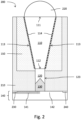
- Figure 2 shows a sectional view of a further pixel 200 which may be similar or identical to the pixel 100, except for the differences described in the following.
- the pixel 200 may comprise a metal layer 114 arranged on the one or more lateral sides 113 of the horn antenna structure 110.
- the metal layer 114 may partially cover the one or more lateral sides 113 or the metal layer 114 may completely cover the one or more lateral sides 113.
- the first and second sides 111, 112 of the horn antenna structure 110 may be free of a metal layer.
- the one or more lateral sides 123 of the waveguide structure 120 may be free of the metal layer 114. However, according to an example it is also possible that the one or more lateral sides 123 of the waveguide structure 120 are at least partially covered by the metal layer 114. For example, an upper part of the one or more lateral sides 123 may be covered by the metal layer 114.
- the metal layer 114 may be configured to reflect incident infrared light and thereby help in guiding photons which enter the horn antenna structure 110 towards the photosensitive structure 130.
- the metal layer 114 may have any suitable thickness.
- the metal layer 114 may have a thickness of 10nm or more, or 50nm or more, or 100nm or more, or 200nm or more.
- the metal layer 114 may for example comprise or consist of Al, AlSi, Cu, ⁇ -Si, Ta, Ti, or W.
- the metal layer 114 comprises a layer stack of different materials.
- the pixel 200 comprises the first dielectric structure 150 and also a second dielectric structure 210.
- the second dielectric structure 210 may at least partially surround the first dielectric structure 150.
- the second dielectric structure 210 may for example completely surround the first dielectric structure 150 on all sides, except for above the first side 111 of the horn antenna structure 110.
- the first and second dielectric structures 150, 210 may have different materials or material compositions.
- the second dielectric structure 210 may comprise a layer stack of different materials (e.g. silicon oxide and silicon nitride) with different etch rates.
- it may therefore be beneficial to fabricate a pit in the second dielectric structure 150 and to fill the pit with the first dielectric structure 150, wherein the first dielectric structure 150 has a homogeneous etch rate.
- the horn antenna structure 110 may then be fabricated in the first dielectric structure, e.g. via etching and subsequent deposition of material. In this case, the horn antenna structure 110 may be arranged fully within the first dielectric structure 150.
- an upper part of the photosensitive structure 130 exhibits an apex, the apex being turned towards the waveguide structure 120.
- the upper part may in particular have a pyramidal shape, wherein the top of the pyramid points towards the waveguide structure 120.
- Such a shape may improve the optical coupling between the waveguide structure 120 and the photosensitive structure 130. For example, such a shape may increase the bandwidth of the coupling.
- the apex or pyramidal shape of the upper part of the photosensitive structure 130 may for example be generated via self-alignment of the Ge-based photosensitive structure 130 during epitaxial growth.
- the pixel 200 may optionally comprise a microlens 220 arranged over the first side 111 of the horn antenna structure 110.
- the microlens 220 may comprise or consist of any suitable material.
- the microlens 220 may comprise or consist of one or more of the materials described with respect to the horn antenna structure 110 or the waveguide structure 120.
- the pixel 200 may also comprise one or more p-contacts 230 and one or more n-contacts 240.
- the at least one n-contact 240 is configured to collect electrons of a photocurrent and the at least one p-contact 230 is configured to collect holes of the photocurrent.
- the at least one p-contact 230 and the at least one n-contact 240 may for example be arranged in the photocurrent collecting structure 140.
- the p-contact 230 and n-contact 240 may comprise or consist of a suitable metallization structure (e.g. comprising or consisting of Al) and may be coupled to evaluation circuitry of the image sensor.
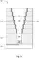
- Figure 3 shows a sectional view of a further pixel 300 which may be similar or identical to the pixel 100 or 200, except for the differences described in the following.
- the horn antenna structure 110 has a stepped shape, wherein the one or more lateral sides 113 comprise vertical sections which are successively shifted inwards, as viewed from above the first side 111. These vertical sections may correspond to individual layers of a stack of layer of the second dielectric structure 210 (indicated by dashed lines in Fig. 3 ).
- the one or more lateral sides 113 may be covered by the metal layer 114.
- the metal layer 114 may be constituted by vias and metal lines comprised in the second dielectric structure 210.
- the vias and metal lines of the second dielectric structure 210 may be configured such that a horn antenna structure 110 is formed.
- the second dielectric structure 210 may be removed (e.g. via etching) inside the horn antenna structure 110. Subsequently, one or more of the materials described with respect to the pixel 100 may be deposited to fill the interior volume of the horn antenna structure 110.
- the pixel 300 does not comprise the metal layer 114.
- the one or more lateral sides 113 of the horn antenna structure 110 may comprise the dielectric material of the second dielectric structure 210.
- the pixel 300 might not comprise the first dielectric structure 150 (as shown in the example of Fig. 3 ).
- the horn antenna structure 110 may be arranged directly within the second dielectric structure 210 in this case.
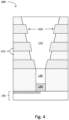
- Figure 4 shows a sectional view of a further pixel 400 which may be similar or identical to the pixels 100 to 300, except for the differences described in the following.
- the horn antenna structure 110 has a corrugated horn shape comprising corrugations 410.
- the shape, size and position of the corrugations 410 may be chosen such that an optimized transmission of photons towards the waveguide structure 120 and the photosensitive structure 130 is achieved.
- the corrugations 410 are constituted by individual layers of the second dielectric structure 210. Fabricating the corrugations 410 may comprise an isotropic etching process, wherein consecutive layers of the second dielectric structure 210 exhibit different etch rates.
- Figure 5 shows a sectional view of a further pixel 500 which may be similar or identical to the pixels 100 to 400, except for the differences described in the following.
- the horn antenna structure 110 has an exponential horn shape.
- the exponential horn shape may for example be fabricated by an etching series using different etching masks.
- the shape of the horn antenna structure 110 may be chosen such that an optimal transmission of photons towards the waveguide structure 120 and the photosensitive structure 130 is obtained.
- the shape of the horn antenna structure 110 may also be a compromise between optimal transmission characteristics and fabrication effort.
- horn antenna structure 110 several examples are shown. However, further shapes for the horn antenna structure 110 are also contemplated, e.g. a dual-mode conical horn shape, a sectoral horn shape, a hybrid mode corrugated horn shape, etc.
- Figure 6 shows a sectional view of a further pixel 600 which may be similar or identical to the pixels 100 to 500, except for the differences described in the following.
- At least one of the electrical contacts is not arranged within the photocurrent collecting structure 140 but instead above the photocurrent collecting structure 140, e.g. within the second dielectric structure 210.
- the photocurrent collecting structure 140 may be free of a p-n junction.
- the photocurrent collecting structure 140 may consist of the n-doped region 142 and the photosensitive structure 130 may comprise p-doped Ge.
- Figure 7 shows a sectional view of a further pixel 700 which may be similar or identical to the pixels 100 to 700, except for the differences described in the following.
- the photosensitive structure 130 comprises a first portion 131 and a second portion 132.
- the first portion 131 comprises or consists of Ge, in particular p-doped Ge
- the second portion 132 comprises or consists of Si, in particular p-doped Si.
- the first portion 131 may for example be epitaxially grown on the photocurrent collecting structure 140 and the second portion 132 may be arranged on the first portion 131.
- the second portion 132 may e.g. comprise epitaxially grown Si or poly-Si.
- the second portion 132 may be coupled to at least one p-contact 230.
- Figure 8 is a flow chart of a method 800 for fabricating an image sensor.
- the method 800 may for example be used to fabricate an image sensor comprising anyone of the pixels 100 to 700.
- the method 800 comprises fabricating at least one pixel, which comprises at 801 an act of fabricating a Ge based photosensitive structure configured to absorb infrared light and generate a photocurrent in response, at 802 an act of arranging a waveguide structure on the photosensitive structure, and at 803 an act of fabricating a horn antenna structure on the waveguide structure, the horn antenna structure comprising a first side, a second side and one or more lateral sides connecting the first side and the second side, wherein the first side faces incoming light and wherein a surface area of the second side is smaller than a surface area of the first side, wherein the horn antenna structure and the waveguide structure are configured to direct incoming infrared light onto the photosensitive structure.
- fabricating the horn antenna structure comprises depositing a second dielectric structure over a Si wafer, etching a pit into the second dielectric structure, then depositing the first dielectric structure in the pit and then etching the first dielectric structure to generate the horn antenna structure.
- Example 1 is an image sensor for sensing infrared light, comprising: at least one pixel, comprising: a horn antenna structure comprising a first side, a second side and one or more lateral sides connecting the first side and the second side, wherein the first side faces incoming light and wherein a surface area of the second side is smaller than a surface area of the first side, a waveguide structure arranged at the second side of the horn antenna structure, and a Ge-based photosensitive structure configured to absorb infrared light and generate a photocurrent in response, wherein the horn antenna structure and the waveguide structure are configured to direct incoming infrared light onto the photosensitive structure.
- Example 2 is the image sensor of example 1, further comprising: a metal layer arranged on the one or more lateral sides of the horn antenna structure.
- Example 3 is the image sensor of example 1 or 2, wherein the waveguide structure comprises or consists of one or more of c-Si, poly-Si, ⁇ -Si, SiO 2 , SiN, Al 2 O 3 and AlN.
- Example 4 is the image sensor of one of the preceding examples, wherein an interior volume of the horn antenna structure comprises or consists of one or more of SiO 2 , SiN, ⁇ -Si, C, air, gas and vacuum.
- Example 5 is the image sensor of example 4, further comprising: a first dielectric structure at least partially surrounding the one or more lateral sides of the horn antenna structure, wherein the first dielectric structure comprises or consists of one or more of SiO 2 , SiN, ⁇ -Si and C.
- Example 6 is the image sensor of example 5, further comprising: a second dielectric structure at least partially surrounding the first dielectric structure, wherein the first and second dielectric structures have different materials or material compositions, and wherein the horn antenna structure is arranged within the first dielectric structure.
- Example 7 is the image sensor of one of the preceding examples, further comprising: a microlens arranged at the first side of the horn antenna structure.
- Example 8 is the image sensor of one of the preceding examples, wherein an upper part of the photosensitive structure exhibits an apex, the apex being turned towards the waveguide structure.
- Example 9 is the image sensor of one of the preceding examples, wherein the horn antenna structure has a shape chosen among one or more of a corrugated horn, an exponential horn, a conical horn, a dual-mode conical horn and a pyramidal horn.
- Example 10 is the image sensor of one of the preceding examples, wherein the photosensitive structure comprises a Si portion arranged on a Ge portion.
- Example 11 is the image sensor of one of the preceding examples, wherein a lateral extension of the photosensitive structure is smaller than a lateral extension of the first side of the horn antenna structure.
- Example 12 is a method for fabricating an image sensor, the method comprising: fabricating at least one pixel by: fabricating a Ge based photosensitive structure configured to absorb infrared light and generate a photocurrent in response, arranging a waveguide structure on the photosensitive structure, and fabricating a horn antenna structure on the waveguide structure, the horn antenna structure comprising a first side, a second side and one or more lateral sides connecting the first side and the second side, wherein the first side faces incoming light and wherein a surface area of the second side is smaller than a surface area of the first side, wherein the horn antenna structure and the waveguide structure are configured to direct incoming infrared light onto the photosensitive structure.
- Example 13 is the method of example 12, wherein fabricating the horn antenna structure comprises: depositing a first dielectric structure over the waveguide structure, and etching the first dielectric structure to generate the horn antenna structure.
- Example 14 is the method of example 13, further comprising: prior to depositing the first dielectric structure, depositing a second dielectric structure over a Si wafer, etching a pit into the second dielectric structure, and depositing the first dielectric structure in the pit.
- Example 15 is the method of one of example 13 or 14, further comprising: after etching the first dielectric structure, filling the horn antenna structure with one or more materials selected from the list comprising SiO 2 , SiN, ⁇ -Si, C, air, gas and vacuum.
- Example 16 is an apparatus comprising means for performing the method according to anyone of examples 12 to 15.
Landscapes
- Waveguide Aerials (AREA)
Abstract
Description
- This disclosure relates in general to an image sensor, in particular to an image sensor comprising a pixel with a horn antenna structure, as well as to a method for fabricating such an image sensor.
- A pixel of an image sensor for infrared light may comprise a Ge-based photosensitive part because at infrared wavelengths Ge offers superior light absorption properties compared to Si. The Ge-based photosensitive part may be heteroepitaxially grown on a Si-based photocurrent collecting part and may be at least partially surrounded by a dielectric part. A larger detector area of the Ge-based photosensitive part may provide improved detector sensitivity. However, such larger detector areas may also increase the leakage current of the pixel because the leakage current may be affected by interface states at the Ge-dielectric interface. It may therefore be desirable to provide a pixel with a reduced Ge surface area, without sacrificing detector sensitivity. Improved image sensors as well as improved methods for fabricating image sensors may help in solving these and other problems.
- The problem on which the invention is based is solved by the features of the independent claims. Further advantageous examples are described in the dependent claims.
- Various aspects pertain to an image sensor for sensing infrared light, comprising: at least one pixel, comprising: a horn antenna structure comprising a first side, a second side and one or more lateral sides connecting the first side and the second side, wherein the first side faces incoming light and wherein a surface area of the second side is smaller than a surface area of the first side, a waveguide structure arranged on the second side of the horn antenna structure, and a Ge-based photosensitive structure configured to absorb infrared light and generate a photocurrent in response, wherein the horn antenna structure and the waveguide structure are configured to direct incoming infrared light onto the photosensitive structure.
- Various aspects pertain to a method for fabricating an image sensor, the method comprising: fabricating at least one pixel by: fabricating a Ge based photosensitive structure configured to absorb infrared light and generate a photocurrent in response, arranging a waveguide structure on the photosensitive structure, and fabricating a horn antenna structure on the waveguide structure, the horn antenna structure comprising a first side, a second side and one or more lateral sides connecting the first side and the second side, wherein the first side faces incoming light and wherein a surface area of the second side is smaller than a surface area of the first side, wherein the horn antenna structure and the waveguide structure are configured to direct incoming infrared light onto the photosensitive structure.
- The accompanying drawings illustrate examples and together with the description serve to explain principles of the disclosure. Other examples and many of the intended advantages of the disclosure will be readily appreciated in view of the following detailed description. The elements of the drawings are not necessarily to scale relative to each other. Identical reference numerals designate corresponding similar parts.
-
Figure 1 shows a sectional view of a pixel for an image sensor, wherein the pixel comprises a horn antenna structure and a waveguide structure configured to direct incident photons towards a photosensitive structure. -
Figure 2 shows a sectional view of a further pixel, wherein the one or more lateral sides of the horn antenna structure are covered by a metal layer. -
Figure 3 shows a sectional view of a further pixel, wherein the horn antenna structure has a stepped shape. -
Figure 4 shows a sectional view of a further pixel, wherein the horn antenna structure has a corrugated horn shape. -
Figure 5 shows a sectional view of a further pixel, wherein the horn antenna structure has an exponential horn shape. -
Figure 6 shows a sectional view of a further pixel, wherein at least one electrical contact of the pixel is arranged within a dielectric structure and is directly coupled to the photosensitive structure. -
Figure 7 shows a sectional view of a further pixel, wherein the photosensitive structure comprises a Ge-based portion and a Si-based portion. -
Figure 8 is a flow chart of an exemplary method for fabricating an image sensor. - In the following detailed description, known structures and elements are shown in schematic form in order to facilitate describing one or more aspects of the disclosure. In this regard, directional terminology, such as "top", "bottom", "left", "right", "upper", "lower" etc., is used with reference to the orientation of the Figure(s) being described.
- In addition, while a particular feature or aspect of an example may be disclosed with respect to only one of several implementations, such feature or aspect may be combined with one or more other features or aspects of the other implementations as may be desired and advantageous for any given or particular application, unless specifically noted otherwise or unless technically restricted. Furthermore, to the extent that the terms "include", "have", "with" or other variants thereof are used in either the detailed description or the claims, such terms are intended to be inclusive in a manner similar to the term "comprise". The terms "coupled" and "connected", along with derivatives thereof may be used. It should be understood that these terms may be used to indicate that two elements cooperate or interact with each other regardless whether they are in direct physical or electrical contact, or they are not in direct contact with each other; intervening elements or layers may be provided between the "bonded", "attached", or "connected" elements. However, it is also possible that the "bonded", "attached", or "connected" elements are in direct contact with each other. Also, the term "exemplary" is merely meant as an example, rather than the best or optimal.
- In several examples layers or layer stacks are applied to one another or materials are applied or deposited onto layers. It should be appreciated that any such terms as "applied" or "deposited" are meant to cover literally all kinds and techniques of applying layers onto each other. In particular, they are meant to cover techniques in which layers are applied at once as a whole as well as techniques in which layers are deposited in a sequential manner like, for example, sputtering, plating, CVD, etc.
- An efficient image sensor as well as an efficient method for fabricating an image sensor may for example reduce material consumption, ohmic losses, chemical waste, etc. and may thus enable energy and/or resource savings. Improved image sensors as well as improved methods for fabricating an image sensor, as specified in this description, may thus at least indirectly contribute to green technology solutions, i.e. climate-friendly solutions providing a mitigation of energy and/or resource use.
-
Figure 1 shows a sectional view of apixel 100 for sensing infrared light. Thepixel 100 may be part of an image sensor configured for sensing infrared light. The image sensor may for example be a CMOS image sensor (CIS) or a time of flight (ToF) sensor, in particular an indirect ToF (iTOF) sensor. The image sensor may comprise asingle pixel 100 or a plurality ofpixels 100, in particular an array ofpixels 100. - The
pixel 100 may for example be configured to be sensitive for near infrared light, for example at a wavelength of about 900nm or more. - The
pixel 100 comprises ahorn antenna structure 110, awaveguide structure 120 and aphotosensitive structure 130. Thepixel 100 may also comprise aphotocurrent collecting structure 140 and/or a firstdielectric structure 150. - The
horn antenna structure 110 comprises afirst side 111, asecond side 112 and one or morelateral sides 113 connecting thefirst side 111 and thesecond side 112. Thefirst side 111 of thehorn antenna structure 110 faces incoming light. Furthermore, a surface area of thesecond side 112 is smaller than a surface area of thefirst side 111. Thefirst side 111 and/or thesecond side 112 may for example have a rectangular outline, a quadratic outline, or a round outline. In other words, thehorn antenna structure 110 may have an essentially pyramidal shape or an essentially funnel shape. - The
horn antenna structure 110 may have any suitable dimensions. For example, thefirst side 111 may have a width in the range of about 1µm to about 10µm. The lower limit of this range may also be about 2pm, about 3µm, about 4µm, or about 5µm and the upper limit may also be about 9pm, about 8pm, about 7µm or about 6µm. Thesecond side 112 may for example have a width in the range of about 0.2pm to about 2µm. The lower limit of this range may also be about 0.3µm, 0.5µm, or 0.7pm and the upper limit may also be about 1.5µm, 1.2µm, 1µm, or 0.8pm. A length of thehorn antenna structure 110, the length being measured between thefirst side 111 and thesecond side 112, may for example be in the range of about 5µm to about 15µm. The lower limit of this range may also be about 7µm, or about 9µm and the upper limit may also be about 13pm, or about 11µm. - According to an example, an interior volume of the
horn antenna structure 110 comprises or consists of one or more of SiO2, SiN, α-Si, C, air, gas and vacuum. In other words, the interior volume of thehorn antenna structure 110 may consist of a solid material or no solid material is arranged within the interior volume of thehorn antenna structure 110. In the latter case, thehorn antenna structure 110 is defined by a horn shaped opening within the firstdielectric structure 150. In the case that the interior volume of thehorn antenna structure 110 comprises a vacuum, a lid may close off thehorn antenna structure 110 at thefirst side 111. According to an example, the interior volume of thehorn antenna structure 110 comprises a layer stack, the layers of the stack comprising materials selected from the aforementioned group. - The
waveguide structure 120 is arranged on thesecond side 112 of thehorn antenna structure 110. Thewaveguide structure 120 may for example have an essentially rectangular outline, or an essentially quadratic outline, or an essentially round outline, as viewed from thesecond side 112 of the horn antenna structure. - The
waveguide structure 120 may have afirst side 121, an oppositesecond side 122 and one or morelateral sides 123 connecting the first andsecond sides first side 121 may be in direct contact with thesecond side 112 of thehorn antenna structure 110. However, it is also possible that e.g. a passivation layer is arranged between thefirst side 121 and thesecond side 112. The one or morelateral sides 123 may be covered by a dielectric material. For example, thefirst dielectric structure 150 and/or a second dielectric structure may at least partially cover the one or morelateral sides 123. - In contrast to the
horn antenna structure 110, a width of thewaveguide structure 120 may be unchanging in every plane between thefirst side 121 and the second side 122 (the width being measured parallel to the first andsecond sides 121, 122). - The
waveguide structure 120 may have any suitable dimensions. For example, thewaveguide structure 120 may have a width that is essentially similar or identical to the width of thesecond side 112 of thehorn antenna structure 110. Thewaveguide structure 120 may have a length, the length being measured between the first andsecond sides - The
waveguide structure 120 may comprise or consist of any suitable material or material composition. For example, thewaveguide structure 120 may comprise or consist of one or more of c-Si, poly-Si, α-Si, SiO2, SiN, Al2O3 and AlN. According to an example, thewaveguide structure 120 comprises a layer stack, the layers of the stack comprising materials selected from the aforementioned group. - According to an example, the
horn antenna structure 110 and thewaveguide structure 120 comprise or consist of the same material or material composition. According to another example, thehorn antenna structure 110 and thewaveguide structure 120 comprise or consist of different materials or different material compositions. In any case, the materials of thehorn antenna structure 110 and the waveguide structure 120 (in particular, the relative permittivity of these materials) may be matched such that a transmission of incident infrared light towards thephotosensitive structure 130 is ensured. - The
photosensitive structure 130 is configured to absorb infrared light and generate a photocurrent in response. Thephotosensitive structure 130 may be an epitaxially-grown structure which comprises or consists of Ge, for example p-doped Ge. According to an example, thephotosensitive structure 130 is epitaxially grown within an aperture in a dielectric material arranged over thephotocurrent collecting structure 140. Aspect ratio trapping (ART) may be used during fabrication of thephotosensitive structure 130 in order to counter defects in the crystalline structure of thephotosensitive structure 130. - An upper end of the
photosensitive structure 130 may be in direct contact with thesecond side 122 of thewaveguide structure 120. However, it is also possible that e.g. a passivation layer is arranged between thesecond side 122 and thephotosensitive structure 130. Furthermore, thephotosensitive structure 130 may be arranged over thephotocurrent collecting structure 140 such that a lower end of thephotosensitive structure 130 is in direct contact with thephotocurrent collecting structure 140. - The
photosensitive structure 130 may be epitaxially grown on thephotocurrent collecting structure 140. Thestructure 130 is termed a "photosensitive" structure because it is a dedicated light absorption part of thepixel 100, wherein incoming photons, in particular infrared photons, are converted into electrons and holes (i.e. a photocurrent). - The
horn antenna structure 110 and thewaveguide structure 120 are configured to direct incoming infrared light onto thephotosensitive structure 130. Thephotosensitive structure 130 may essentially have the same width or the same diameter as thewaveguide structure 120, respectively thesecond side 112 of thehorn antenna structure 110. In other words, the width or the diameter of thefirst side 111 of thehorn antenna structure 110 is larger than the width or the diameter of thephotosensitive structure 130. The detector surface of thepixel 100 is defined by the surface area of thefirst side 111 of thehorn antenna structure 110. By providing thehorn antenna structure 110 and thewaveguide structure 120, a comparatively smallphotosensitive structure 130 may be used. This may help in reducing a leakage current in thepixel 100, because the leakage current may be affected by interface states at the Ge-dielectric interface. Furthermore, the process time for Ge epitaxy may be relatively long and by reducing the required size of the Ge structure, the fabrication costs of an image sensor comprising thepixel 100 may be reduced. - The
photocurrent collecting structure 140 may comprise or consist of Si and it may e.g. be a structure epitaxially grown on bulk Si. Thephotocurrent collecting structure 140 may for example comprise a p-dopedregion 141 and an n-dopedregion 142. Thephotocurrent collecting structure 140 may for example comprise a p-n junction, wherein thephotosensitive structure 130 is arranged above the p-n junction. The n-dopedregion 142 may be configured to conduct electrons of the photocurrent to at least one n-contact of thepixel 100 and the p-dopedregion 141 may be configured to conduct holes of the photocurrent to at least one p-contact of thepixel 100. Thepixel 100 may furthermore comprise demodulation gates configured to direct electrons of the photocurrent to a particular n-contact of a plurality of n-contacts, respectively to direct holes of the photocurrent to a particular p-contact of a plurality of p-contacts (indirect time of flight measurement). - The
first dielectric structure 150 may for example at least partially surround the one or morelateral sides 113 of thehorn antenna structure 110. Thefirst dielectric structure 150 may for example comprise or consist of one or more of SiO2, SiN, α-Si and C. - The composition of the
horn antenna structure 110 on the one hand and the composition of thefirst dielectric structure 150 on the other hand (in particular, the relative permittivity of the respective materials) may be matched such that incident infrared light is totally reflected at the one or morelateral sides 113 of thehorn antenna structure 110. -
Figure 2 shows a sectional view of afurther pixel 200 which may be similar or identical to thepixel 100, except for the differences described in the following. - In particular, the
pixel 200 may comprise ametal layer 114 arranged on the one or morelateral sides 113 of thehorn antenna structure 110. Themetal layer 114 may partially cover the one or morelateral sides 113 or themetal layer 114 may completely cover the one or morelateral sides 113. The first andsecond sides horn antenna structure 110 may be free of a metal layer. - The one or more
lateral sides 123 of thewaveguide structure 120 may be free of themetal layer 114. However, according to an example it is also possible that the one or morelateral sides 123 of thewaveguide structure 120 are at least partially covered by themetal layer 114. For example, an upper part of the one or morelateral sides 123 may be covered by themetal layer 114. - The
metal layer 114 may be configured to reflect incident infrared light and thereby help in guiding photons which enter thehorn antenna structure 110 towards thephotosensitive structure 130. - The
metal layer 114 may have any suitable thickness. For example, themetal layer 114 may have a thickness of 10nm or more, or 50nm or more, or 100nm or more, or 200nm or more. Themetal layer 114 may for example comprise or consist of Al, AlSi, Cu, α-Si, Ta, Ti, or W. According to an example, themetal layer 114 comprises a layer stack of different materials. - According to the example shown in
Fig. 2 , thepixel 200 comprises thefirst dielectric structure 150 and also asecond dielectric structure 210. Thesecond dielectric structure 210 may at least partially surround thefirst dielectric structure 150. As shown inFig. 2 , thesecond dielectric structure 210 may for example completely surround thefirst dielectric structure 150 on all sides, except for above thefirst side 111 of thehorn antenna structure 110. - The first and second
dielectric structures second dielectric structure 210 may comprise a layer stack of different materials (e.g. silicon oxide and silicon nitride) with different etch rates. In order to fabricate thehorn antenna structure 110, it may therefore be beneficial to fabricate a pit in thesecond dielectric structure 150 and to fill the pit with thefirst dielectric structure 150, wherein thefirst dielectric structure 150 has a homogeneous etch rate. Thehorn antenna structure 110 may then be fabricated in the first dielectric structure, e.g. via etching and subsequent deposition of material. In this case, thehorn antenna structure 110 may be arranged fully within thefirst dielectric structure 150. - According to the example shown in
Fig. 2 , an upper part of thephotosensitive structure 130 exhibits an apex, the apex being turned towards thewaveguide structure 120. The upper part may in particular have a pyramidal shape, wherein the top of the pyramid points towards thewaveguide structure 120. Such a shape may improve the optical coupling between thewaveguide structure 120 and thephotosensitive structure 130. For example, such a shape may increase the bandwidth of the coupling. - The apex or pyramidal shape of the upper part of the
photosensitive structure 130 may for example be generated via self-alignment of the Ge-basedphotosensitive structure 130 during epitaxial growth. - The
pixel 200 may optionally comprise amicrolens 220 arranged over thefirst side 111 of thehorn antenna structure 110. Themicrolens 220 may comprise or consist of any suitable material. For example, themicrolens 220 may comprise or consist of one or more of the materials described with respect to thehorn antenna structure 110 or thewaveguide structure 120. - The
pixel 200 may also comprise one or more p-contacts 230 and one or more n-contacts 240. The at least one n-contact 240 is configured to collect electrons of a photocurrent and the at least one p-contact 230 is configured to collect holes of the photocurrent. - The at least one p-
contact 230 and the at least one n-contact 240 may for example be arranged in thephotocurrent collecting structure 140. The p-contact 230 and n-contact 240 may comprise or consist of a suitable metallization structure (e.g. comprising or consisting of Al) and may be coupled to evaluation circuitry of the image sensor. -
Figure 3 shows a sectional view of afurther pixel 300 which may be similar or identical to thepixel - In particular, in the
pixel 300 thehorn antenna structure 110 has a stepped shape, wherein the one or morelateral sides 113 comprise vertical sections which are successively shifted inwards, as viewed from above thefirst side 111. These vertical sections may correspond to individual layers of a stack of layer of the second dielectric structure 210 (indicated by dashed lines inFig. 3 ). - According to the example shown in
Fig. 3 , the one or morelateral sides 113 may be covered by themetal layer 114. In thepixel 300, themetal layer 114 may be constituted by vias and metal lines comprised in thesecond dielectric structure 210. In other words, the vias and metal lines of thesecond dielectric structure 210 may be configured such that ahorn antenna structure 110 is formed. During fabrication of thepixel 300, thesecond dielectric structure 210 may be removed (e.g. via etching) inside thehorn antenna structure 110. Subsequently, one or more of the materials described with respect to thepixel 100 may be deposited to fill the interior volume of thehorn antenna structure 110. - According to an example, the
pixel 300 does not comprise themetal layer 114. In other words, the one or morelateral sides 113 of thehorn antenna structure 110 may comprise the dielectric material of thesecond dielectric structure 210. - It should be noted that the
pixel 300 might not comprise the first dielectric structure 150 (as shown in the example ofFig. 3 ). In other words, thehorn antenna structure 110 may be arranged directly within thesecond dielectric structure 210 in this case. -
Figure 4 shows a sectional view of afurther pixel 400 which may be similar or identical to thepixels 100 to 300, except for the differences described in the following. - In particular, in the
pixel 400 thehorn antenna structure 110 has a corrugated hornshape comprising corrugations 410. The shape, size and position of thecorrugations 410 may be chosen such that an optimized transmission of photons towards thewaveguide structure 120 and thephotosensitive structure 130 is achieved. - According to an example, the
corrugations 410 are constituted by individual layers of thesecond dielectric structure 210. Fabricating thecorrugations 410 may comprise an isotropic etching process, wherein consecutive layers of thesecond dielectric structure 210 exhibit different etch rates. -
Figure 5 shows a sectional view of afurther pixel 500 which may be similar or identical to thepixels 100 to 400, except for the differences described in the following. - In particular, in the
pixel 500 thehorn antenna structure 110 has an exponential horn shape. The exponential horn shape may for example be fabricated by an etching series using different etching masks. - In general, the shape of the
horn antenna structure 110 may be chosen such that an optimal transmission of photons towards thewaveguide structure 120 and thephotosensitive structure 130 is obtained. However, the shape of thehorn antenna structure 110 may also be a compromise between optimal transmission characteristics and fabrication effort. - In the
Figs. 1 to 5 , several examples of shapes for thehorn antenna structure 110 are shown. However, further shapes for thehorn antenna structure 110 are also contemplated, e.g. a dual-mode conical horn shape, a sectoral horn shape, a hybrid mode corrugated horn shape, etc. -
Figure 6 shows a sectional view of afurther pixel 600 which may be similar or identical to thepixels 100 to 500, except for the differences described in the following. - In particular, in the
pixel 600 at least one of the electrical contacts (e.g. one or more p-contacts 230) is not arranged within thephotocurrent collecting structure 140 but instead above thephotocurrent collecting structure 140, e.g. within thesecond dielectric structure 210. In this case, thephotocurrent collecting structure 140 may be free of a p-n junction. Instead, thephotocurrent collecting structure 140 may consist of the n-dopedregion 142 and thephotosensitive structure 130 may comprise p-doped Ge. -
Figure 7 shows a sectional view of afurther pixel 700 which may be similar or identical to thepixels 100 to 700, except for the differences described in the following. - In particular, in the
pixel 700 thephotosensitive structure 130 comprises afirst portion 131 and asecond portion 132. Thefirst portion 131 comprises or consists of Ge, in particular p-doped Ge, and thesecond portion 132 comprises or consists of Si, in particular p-doped Si. Thefirst portion 131 may for example be epitaxially grown on thephotocurrent collecting structure 140 and thesecond portion 132 may be arranged on thefirst portion 131. Thesecond portion 132 may e.g. comprise epitaxially grown Si or poly-Si. Furthermore, thesecond portion 132 may be coupled to at least one p-contact 230. -
Figure 8 is a flow chart of amethod 800 for fabricating an image sensor. Themethod 800 may for example be used to fabricate an image sensor comprising anyone of thepixels 100 to 700. - The
method 800 comprises fabricating at least one pixel, which comprises at 801 an act of fabricating a Ge based photosensitive structure configured to absorb infrared light and generate a photocurrent in response, at 802 an act of arranging a waveguide structure on the photosensitive structure, and at 803 an act of fabricating a horn antenna structure on the waveguide structure, the horn antenna structure comprising a first side, a second side and one or more lateral sides connecting the first side and the second side, wherein the first side faces incoming light and wherein a surface area of the second side is smaller than a surface area of the first side, wherein the horn antenna structure and the waveguide structure are configured to direct incoming infrared light onto the photosensitive structure. - According to an example of the
method 800, fabricating the horn antenna structure comprises depositing a second dielectric structure over a Si wafer, etching a pit into the second dielectric structure, then depositing the first dielectric structure in the pit and then etching the first dielectric structure to generate the horn antenna structure. - In the following, the image sensor and the method for fabricating an image sensor are further explained using specific examples.
- Example 1 is an image sensor for sensing infrared light, comprising: at least one pixel, comprising: a horn antenna structure comprising a first side, a second side and one or more lateral sides connecting the first side and the second side, wherein the first side faces incoming light and wherein a surface area of the second side is smaller than a surface area of the first side, a waveguide structure arranged at the second side of the horn antenna structure, and a Ge-based photosensitive structure configured to absorb infrared light and generate a photocurrent in response, wherein the horn antenna structure and the waveguide structure are configured to direct incoming infrared light onto the photosensitive structure.
- Example 2 is the image sensor of example 1, further comprising: a metal layer arranged on the one or more lateral sides of the horn antenna structure.
- Example 3 is the image sensor of example 1 or 2, wherein the waveguide structure comprises or consists of one or more of c-Si, poly-Si, α-Si, SiO2, SiN, Al2O3 and AlN.
- Example 4 is the image sensor of one of the preceding examples, wherein an interior volume of the horn antenna structure comprises or consists of one or more of SiO2, SiN, α-Si, C, air, gas and vacuum.
- Example 5 is the image sensor of example 4, further comprising: a first dielectric structure at least partially surrounding the one or more lateral sides of the horn antenna structure, wherein the first dielectric structure comprises or consists of one or more of SiO2, SiN, α-Si and C.
- Example 6 is the image sensor of example 5, further comprising: a second dielectric structure at least partially surrounding the first dielectric structure, wherein the first and second dielectric structures have different materials or material compositions, and wherein the horn antenna structure is arranged within the first dielectric structure.
- Example 7 is the image sensor of one of the preceding examples, further comprising: a microlens arranged at the first side of the horn antenna structure.
- Example 8 is the image sensor of one of the preceding examples, wherein an upper part of the photosensitive structure exhibits an apex, the apex being turned towards the waveguide structure.
- Example 9 is the image sensor of one of the preceding examples, wherein the horn antenna structure has a shape chosen among one or more of a corrugated horn, an exponential horn, a conical horn, a dual-mode conical horn and a pyramidal horn.
- Example 10 is the image sensor of one of the preceding examples, wherein the photosensitive structure comprises a Si portion arranged on a Ge portion.
- Example 11 is the image sensor of one of the preceding examples, wherein a lateral extension of the photosensitive structure is smaller than a lateral extension of the first side of the horn antenna structure.
- Example 12 is a method for fabricating an image sensor, the method comprising: fabricating at least one pixel by: fabricating a Ge based photosensitive structure configured to absorb infrared light and generate a photocurrent in response, arranging a waveguide structure on the photosensitive structure, and fabricating a horn antenna structure on the waveguide structure, the horn antenna structure comprising a first side, a second side and one or more lateral sides connecting the first side and the second side, wherein the first side faces incoming light and wherein a surface area of the second side is smaller than a surface area of the first side, wherein the horn antenna structure and the waveguide structure are configured to direct incoming infrared light onto the photosensitive structure.
- Example 13 is the method of example 12, wherein fabricating the horn antenna structure comprises: depositing a first dielectric structure over the waveguide structure, and etching the first dielectric structure to generate the horn antenna structure.
- Example 14 is the method of example 13, further comprising: prior to depositing the first dielectric structure, depositing a second dielectric structure over a Si wafer, etching a pit into the second dielectric structure, and depositing the first dielectric structure in the pit.
- Example 15 is the method of one of example 13 or 14, further comprising: after etching the first dielectric structure, filling the horn antenna structure with one or more materials selected from the list comprising SiO2, SiN, α-Si, C, air, gas and vacuum.
- Example 16 is an apparatus comprising means for performing the method according to anyone of examples 12 to 15.
- While the disclosure has been illustrated and described with respect to one or more implementations, alterations and/or modifications may be made to the illustrated examples without departing from the spirit and scope of the appended claims. In particular regard to the various functions performed by the above described components or structures (assemblies, devices, circuits, systems, etc.), the terms (including a reference to a "means") used to describe such components are intended to correspond, unless otherwise indicated, to any component or structure which performs the specified function of the described component (e.g., that is functionally equivalent), even though not structurally equivalent to the disclosed structure which performs the function in the herein illustrated exemplary implementations of the disclosure.
Claims (15)
- An image sensor for sensing infrared light, comprising:
at least one pixel (100), comprising:a horn antenna structure (110) comprising a first side (111), a second side (112) and one or more lateral sides (113) connecting the first side (111) and the second side (112), wherein the first side (111) faces incoming light and wherein a surface area of the second side (112) is smaller than a surface area of the first side (111),a waveguide structure (120) arranged at the second side (112) of the horn antenna structure (110), anda Ge-based photosensitive structure (130) configured to absorb infrared light and generate a photocurrent in response,wherein the horn antenna structure (110) and the waveguide structure (120) are configured to direct incoming infrared light onto the photosensitive structure (130). - The image sensor of claim 1, further comprising:
a metal layer (114) arranged on the one or more lateral sides (113) of the horn antenna structure (110). - The image sensor of claim 1 or 2, wherein the waveguide structure comprises or consists of one or more of c-Si, poly-Si, α-Si, SiO2, SiN, Al2O3 and AlN.
- The image sensor of one of the preceding claims, wherein an interior volume of the horn antenna structure (110) comprises or consists of one or more of SiO2, SiN, α-Si, C, air, gas and vacuum.
- The image sensor of claim 4, further comprising:a first dielectric structure (150) at least partially surrounding the one or more lateral sides (113) of the horn antenna structure (110),wherein the first dielectric structure (150) comprises or consists of one or more of SiO2, SiN, α-Si and C.
- The image sensor of claim 5, further comprising:a second dielectric structure (210) at least partially surrounding the first dielectric structure (150), wherein the first and second dielectric structures (150, 210) have different materials or material compositions, andwherein the horn antenna structure (110) is arranged within the first dielectric structure (150).
- The image sensor of one of the preceding claims, further comprising:
a microlens (220) arranged at the first side (111) of the horn antenna structure (110). - The image sensor of one of the preceding claims, wherein an upper part of the photosensitive structure (130) exhibits an apex, the apex being turned towards the waveguide structure (120).
- The image sensor of one of the preceding claims, wherein the horn antenna structure (110) has a shape chosen among one or more of a corrugated horn, an exponential horn, a conical horn, a dual-mode conical horn and a pyramidal horn.
- The image sensor of one of the preceding claims, wherein the photosensitive structure (130) comprises a Si portion (132) arranged on a Ge portion (131).
- The image sensor of one of the preceding claims, wherein a lateral extension of the photosensitive structure (130) is smaller than a lateral extension of the first side (111) of the horn antenna structure (110).
- A method (800) for fabricating an image sensor, the method (800) comprising:fabricating at least one pixel by:fabricating (801) a Ge based photosensitive structure configured to absorb infrared light and generate a photocurrent in response,arranging (802) a waveguide structure on the photosensitive structure, andfabricating (803) a horn antenna structure on the waveguide structure, the horn antenna structure comprising a first side, a second side and one or more lateral sides connecting the first side and the second side, wherein the first side faces incoming light and wherein a surface area of the second side is smaller than a surface area of the first side,wherein the horn antenna structure and the waveguide structure are configured to direct incoming infrared light onto the photosensitive structure.
- The method (800) of claim 12, wherein fabricating (803) the horn antenna structure comprises:depositing a first dielectric structure over the waveguide structure, andetching the first dielectric structure to generate the horn antenna structure.
- The method (800) of claim 13, further comprising:prior to depositing the first dielectric structure, depositing a second dielectric structure over a Si wafer,etching a pit into the second dielectric structure, anddepositing the first dielectric structure in the pit.
- The method (800) of one of claim 13 or 14, further comprising:
after etching the first dielectric structure, filling the horn antenna structure with one or more materials selected from the list comprising SiO2, SiN, α-Si, C, air, gas and vacuum.
Priority Applications (3)
| Application Number | Priority Date | Filing Date | Title |
|---|---|---|---|
| EP22179200.5A EP4293722A1 (en) | 2022-06-15 | 2022-06-15 | Image sensor comprising a pixel with a horn antenna structure and method for fabricating the same |
| US18/325,679 US20230411859A1 (en) | 2022-06-15 | 2023-05-30 | Image sensor comprising a pixel with a horn antenna structure and method for fabricating the same |
| CN202310701263.4A CN117238935A (en) | 2022-06-15 | 2023-06-14 | Image sensor including pixels having horn-shaped antenna structures and method of manufacturing the same |
Applications Claiming Priority (1)
| Application Number | Priority Date | Filing Date | Title |
|---|---|---|---|
| EP22179200.5A EP4293722A1 (en) | 2022-06-15 | 2022-06-15 | Image sensor comprising a pixel with a horn antenna structure and method for fabricating the same |
Publications (1)
| Publication Number | Publication Date |
|---|---|
| EP4293722A1 true EP4293722A1 (en) | 2023-12-20 |
Family
ID=82067711
Family Applications (1)
| Application Number | Title | Priority Date | Filing Date |
|---|---|---|---|
| EP22179200.5A Pending EP4293722A1 (en) | 2022-06-15 | 2022-06-15 | Image sensor comprising a pixel with a horn antenna structure and method for fabricating the same |
Country Status (3)
| Country | Link |
|---|---|
| US (1) | US20230411859A1 (en) |
| EP (1) | EP4293722A1 (en) |
| CN (1) | CN117238935A (en) |
Citations (2)
| Publication number | Priority date | Publication date | Assignee | Title |
|---|---|---|---|---|
| US20150229852A1 (en) * | 2012-09-16 | 2015-08-13 | Shalom Wertsberger | Pixel structure using a tapered core waveguide, image sensors and camera using same |
| US20210242354A1 (en) * | 2013-05-22 | 2021-08-05 | W&Wsens Devices, Inc. | Microstructure enhanced absorption photosensitive devices |
Family Cites Families (9)
| Publication number | Priority date | Publication date | Assignee | Title |
|---|---|---|---|---|
| US3624655A (en) * | 1968-11-05 | 1971-11-30 | Kobusai Denkshin Denwa Kk | Horn antenna |
| US3698000A (en) * | 1971-05-06 | 1972-10-10 | Rca Corp | Flexible and slidable waveguide feed system for a radiating horn antenna |
| US4700195A (en) * | 1985-10-01 | 1987-10-13 | Harris Corporation | Waveguide fed composite horn antenna |
| JPH0693569B2 (en) * | 1989-09-26 | 1994-11-16 | ユピテル工業株式会社 | Microwave detector |
| JP4029217B2 (en) * | 2005-01-20 | 2008-01-09 | 株式会社村田製作所 | Waveguide horn array antenna and radar apparatus |
| US7852277B2 (en) * | 2007-08-03 | 2010-12-14 | Lockheed Martin Corporation | Circularly polarized horn antenna |
| US7835600B1 (en) * | 2008-07-18 | 2010-11-16 | Hrl Laboratories, Llc | Microwave receiver front-end assembly and array |
| JP6033520B1 (en) * | 2015-06-03 | 2016-11-30 | 三菱電機株式会社 | Horn antenna |
| KR102580323B1 (en) * | 2022-02-24 | 2023-09-19 | 주식회사 센서뷰 | Horn Antenna for Millimeter Wave |
-
2022
- 2022-06-15 EP EP22179200.5A patent/EP4293722A1/en active Pending
-
2023
- 2023-05-30 US US18/325,679 patent/US20230411859A1/en active Pending
- 2023-06-14 CN CN202310701263.4A patent/CN117238935A/en active Pending
Patent Citations (2)
| Publication number | Priority date | Publication date | Assignee | Title |
|---|---|---|---|---|
| US20150229852A1 (en) * | 2012-09-16 | 2015-08-13 | Shalom Wertsberger | Pixel structure using a tapered core waveguide, image sensors and camera using same |
| US20210242354A1 (en) * | 2013-05-22 | 2021-08-05 | W&Wsens Devices, Inc. | Microstructure enhanced absorption photosensitive devices |
Also Published As
| Publication number | Publication date |
|---|---|
| US20230411859A1 (en) | 2023-12-21 |
| CN117238935A (en) | 2023-12-15 |
Similar Documents
| Publication | Publication Date | Title |
|---|---|---|
| US7425460B2 (en) | Method for implementation of back-illuminated CMOS or CCD imagers | |
| CN113053933A (en) | Method and structure for improving image sensor crosstalk | |
| US9130072B1 (en) | Backside illuminated image sensor and method of manufacturing the same | |
| US20230197758A1 (en) | Photodetecting device with enhanced collection efficiency | |
| US20100044677A1 (en) | Photodiode array, method of manufacturing the same, and detecting device | |
| JP2009038352A (en) | Photodetection element, imaging element, photodetection method, and imaging method | |
| WO2013062687A1 (en) | Backside-thinned image sensor using a12o3 surface passivation | |
| US8399820B2 (en) | Multicolor detectors and applications thereof | |
| CN120358813B (en) | Backside-illuminated image sensor, preparation method thereof and electronic equipment | |
| WO2018022622A1 (en) | Infrared detector devices and focal plane arrays having a transparent common ground structure and methods of fabricating the same | |
| US20100327386A1 (en) | Photodiode array, image pickup device, and manufacturing method | |
| US11955501B2 (en) | Image sensor with improved light conversion efficiency | |
| US20020110950A1 (en) | Method of fabricating a light receiving device | |
| EP3707755B1 (en) | Germanium on insulator for cmos imagers in the short wave infrared | |
| US8125043B2 (en) | Photodetector element | |
| US5449944A (en) | Semiconductor infrared image pickup device and method of fabricating the same | |
| US20230411859A1 (en) | Image sensor comprising a pixel with a horn antenna structure and method for fabricating the same | |
| JP2009283637A (en) | Solid state imaging device and method of manufacturing the same | |
| CN1330004C (en) | Semiconductor optical recieving device and manufacturing method thereof | |
| EP4145540A1 (en) | Time of flight sensor and method for fabricating a time of flight sensor | |
| Martin et al. | InGaAs/InP focal plane arrays for visible light imaging | |
| US6589848B1 (en) | Photodetector device and method for manufacturing the same | |
| WO2023110412A1 (en) | Sensor for sensing visible and infrared images, and method for producing such a sensor | |
| CN109742183A (en) | A kind of photodetector and preparation method thereof | |
| EP4362098A1 (en) | Active pixel sensor and method for fabricating an active pixel sensor |
Legal Events
| Date | Code | Title | Description |
|---|---|---|---|
| PUAI | Public reference made under article 153(3) epc to a published international application that has entered the european phase |
Free format text: ORIGINAL CODE: 0009012 |
|
| STAA | Information on the status of an ep patent application or granted ep patent |
Free format text: STATUS: THE APPLICATION HAS BEEN PUBLISHED |
|
| AK | Designated contracting states |
Kind code of ref document: A1 Designated state(s): AL AT BE BG CH CY CZ DE DK EE ES FI FR GB GR HR HU IE IS IT LI LT LU LV MC MK MT NL NO PL PT RO RS SE SI SK SM TR |
|
| STAA | Information on the status of an ep patent application or granted ep patent |
Free format text: STATUS: REQUEST FOR EXAMINATION WAS MADE |
|
| 17P | Request for examination filed |
Effective date: 20240221 |
|
| RBV | Designated contracting states (corrected) |
Designated state(s): AL AT BE BG CH CY CZ DE DK EE ES FI FR GB GR HR HU IE IS IT LI LT LU LV MC MK MT NL NO PL PT RO RS SE SI SK SM TR |
|
| REG | Reference to a national code |
Ref country code: DE Ref legal event code: R079 Free format text: PREVIOUS MAIN CLASS: H01L0027146000 Ipc: H10F0039000000 |
|
| RIC1 | Information provided on ipc code assigned before grant |
Ipc: H10F 39/00 20250101AFI20260401BHEP |
|
| GRAP | Despatch of communication of intention to grant a patent |
Free format text: ORIGINAL CODE: EPIDOSNIGR1 |
|
| STAA | Information on the status of an ep patent application or granted ep patent |
Free format text: STATUS: GRANT OF PATENT IS INTENDED |