EP4290770A1 - Variable gain amplifier - Google Patents
Variable gain amplifier Download PDFInfo
- Publication number
- EP4290770A1 EP4290770A1 EP23153866.1A EP23153866A EP4290770A1 EP 4290770 A1 EP4290770 A1 EP 4290770A1 EP 23153866 A EP23153866 A EP 23153866A EP 4290770 A1 EP4290770 A1 EP 4290770A1
- Authority
- EP
- European Patent Office
- Prior art keywords
- circuit
- variable
- transistor
- gain amplifier
- variable attenuation
- Prior art date
- Legal status (The legal status is an assumption and is not a legal conclusion. Google has not performed a legal analysis and makes no representation as to the accuracy of the status listed.)
- Granted
Links
Images






Classifications
-
- H—ELECTRICITY
- H03—ELECTRONIC CIRCUITRY
- H03F—AMPLIFIERS
- H03F3/00—Amplifiers with only discharge tubes or only semiconductor devices as amplifying elements
- H03F3/45—Differential amplifiers
- H03F3/45071—Differential amplifiers with semiconductor devices only
- H03F3/45076—Differential amplifiers with semiconductor devices only characterised by the way of implementation of the active amplifying circuit in the differential amplifier
- H03F3/4508—Differential amplifiers with semiconductor devices only characterised by the way of implementation of the active amplifying circuit in the differential amplifier using bipolar transistors as the active amplifying circuit
- H03F3/45085—Long tailed pairs
-
- H—ELECTRICITY
- H03—ELECTRONIC CIRCUITRY
- H03F—AMPLIFIERS
- H03F3/00—Amplifiers with only discharge tubes or only semiconductor devices as amplifying elements
- H03F3/20—Power amplifiers, e.g. Class B amplifiers, Class C amplifiers
- H03F3/24—Power amplifiers, e.g. Class B amplifiers, Class C amplifiers of transmitter output stages
- H03F3/245—Power amplifiers, e.g. Class B amplifiers, Class C amplifiers of transmitter output stages with semiconductor devices only
-
- H—ELECTRICITY
- H03—ELECTRONIC CIRCUITRY
- H03F—AMPLIFIERS
- H03F1/00—Details of amplifiers with only discharge tubes, only semiconductor devices or only unspecified devices as amplifying elements
- H03F1/56—Modifications of input or output impedances, not otherwise provided for
-
- H—ELECTRICITY
- H03—ELECTRONIC CIRCUITRY
- H03F—AMPLIFIERS
- H03F3/00—Amplifiers with only discharge tubes or only semiconductor devices as amplifying elements
- H03F3/189—High-frequency amplifiers, e.g. radio frequency amplifiers
- H03F3/19—High-frequency amplifiers, e.g. radio frequency amplifiers with semiconductor devices only
-
- H—ELECTRICITY
- H03—ELECTRONIC CIRCUITRY
- H03F—AMPLIFIERS
- H03F3/00—Amplifiers with only discharge tubes or only semiconductor devices as amplifying elements
- H03F3/26—Push-pull amplifiers; Phase-splitters therefor
- H03F3/265—Push-pull amplifiers; Phase-splitters therefor with field-effect transistors only
-
- H—ELECTRICITY
- H03—ELECTRONIC CIRCUITRY
- H03F—AMPLIFIERS
- H03F3/00—Amplifiers with only discharge tubes or only semiconductor devices as amplifying elements
- H03F3/45—Differential amplifiers
- H03F3/45071—Differential amplifiers with semiconductor devices only
- H03F3/45076—Differential amplifiers with semiconductor devices only characterised by the way of implementation of the active amplifying circuit in the differential amplifier
- H03F3/45179—Differential amplifiers with semiconductor devices only characterised by the way of implementation of the active amplifying circuit in the differential amplifier using MOSFET transistors as the active amplifying circuit
- H03F3/45183—Long tailed pairs
-
- H—ELECTRICITY
- H03—ELECTRONIC CIRCUITRY
- H03F—AMPLIFIERS
- H03F3/00—Amplifiers with only discharge tubes or only semiconductor devices as amplifying elements
- H03F3/45—Differential amplifiers
- H03F3/45071—Differential amplifiers with semiconductor devices only
- H03F3/45076—Differential amplifiers with semiconductor devices only characterised by the way of implementation of the active amplifying circuit in the differential amplifier
- H03F3/45475—Differential amplifiers with semiconductor devices only characterised by the way of implementation of the active amplifying circuit in the differential amplifier using IC blocks as the active amplifying circuit
-
- H—ELECTRICITY
- H03—ELECTRONIC CIRCUITRY
- H03G—CONTROL OF AMPLIFICATION
- H03G1/00—Details of arrangements for controlling amplification
- H03G1/0005—Circuits characterised by the type of controlling devices operated by a controlling current or voltage signal
- H03G1/0017—Circuits characterised by the type of controlling devices operated by a controlling current or voltage signal the device being at least one of the amplifying solid-state elements
- H03G1/0023—Circuits characterised by the type of controlling devices operated by a controlling current or voltage signal the device being at least one of the amplifying solid-state elements in emitter-coupled or cascode amplifiers
-
- H—ELECTRICITY
- H03—ELECTRONIC CIRCUITRY
- H03G—CONTROL OF AMPLIFICATION
- H03G1/00—Details of arrangements for controlling amplification
- H03G1/0005—Circuits characterised by the type of controlling devices operated by a controlling current or voltage signal
- H03G1/0035—Circuits characterised by the type of controlling devices operated by a controlling current or voltage signal using continuously variable impedance elements
- H03G1/007—Circuits characterised by the type of controlling devices operated by a controlling current or voltage signal using continuously variable impedance elements using field-effect transistors [FET]
-
- H—ELECTRICITY
- H03—ELECTRONIC CIRCUITRY
- H03G—CONTROL OF AMPLIFICATION
- H03G1/00—Details of arrangements for controlling amplification
- H03G1/0005—Circuits characterised by the type of controlling devices operated by a controlling current or voltage signal
- H03G1/0088—Circuits characterised by the type of controlling devices operated by a controlling current or voltage signal using discontinuously variable devices, e.g. switch-operated
-
- H—ELECTRICITY
- H03—ELECTRONIC CIRCUITRY
- H03G—CONTROL OF AMPLIFICATION
- H03G3/00—Gain control in amplifiers or frequency changers
- H03G3/20—Automatic control
- H03G3/30—Automatic control in amplifiers having semiconductor devices
-
- H—ELECTRICITY
- H03—ELECTRONIC CIRCUITRY
- H03G—CONTROL OF AMPLIFICATION
- H03G3/00—Gain control in amplifiers or frequency changers
- H03G3/20—Automatic control
- H03G3/30—Automatic control in amplifiers having semiconductor devices
- H03G3/3005—Automatic control in amplifiers having semiconductor devices in amplifiers suitable for low-frequencies, e.g. audio amplifiers
- H03G3/301—Automatic control in amplifiers having semiconductor devices in amplifiers suitable for low-frequencies, e.g. audio amplifiers the gain being continuously variable
- H03G3/3015—Automatic control in amplifiers having semiconductor devices in amplifiers suitable for low-frequencies, e.g. audio amplifiers the gain being continuously variable using diodes or transistors
-
- H—ELECTRICITY
- H03—ELECTRONIC CIRCUITRY
- H03F—AMPLIFIERS
- H03F2200/00—Indexing scheme relating to amplifiers
- H03F2200/211—Indexing scheme relating to amplifiers the input of an amplifier can be attenuated by a continuously controlled transistor attenuator
-
- H—ELECTRICITY
- H03—ELECTRONIC CIRCUITRY
- H03F—AMPLIFIERS
- H03F2200/00—Indexing scheme relating to amplifiers
- H03F2200/222—A circuit being added at the input of an amplifier to adapt the input impedance of the amplifier
-
- H—ELECTRICITY
- H03—ELECTRONIC CIRCUITRY
- H03F—AMPLIFIERS
- H03F2200/00—Indexing scheme relating to amplifiers
- H03F2200/318—A matching circuit being used as coupling element between two amplifying stages
-
- H—ELECTRICITY
- H03—ELECTRONIC CIRCUITRY
- H03F—AMPLIFIERS
- H03F2200/00—Indexing scheme relating to amplifiers
- H03F2200/387—A circuit being added at the output of an amplifier to adapt the output impedance of the amplifier
-
- H—ELECTRICITY
- H03—ELECTRONIC CIRCUITRY
- H03F—AMPLIFIERS
- H03F2200/00—Indexing scheme relating to amplifiers
- H03F2200/405—Indexing scheme relating to amplifiers the output amplifying stage of an amplifier comprising more than three power stages
-
- H—ELECTRICITY
- H03—ELECTRONIC CIRCUITRY
- H03F—AMPLIFIERS
- H03F2200/00—Indexing scheme relating to amplifiers
- H03F2200/408—Indexing scheme relating to amplifiers the output amplifying stage of an amplifier comprising three power stages
-
- H—ELECTRICITY
- H03—ELECTRONIC CIRCUITRY
- H03F—AMPLIFIERS
- H03F2200/00—Indexing scheme relating to amplifiers
- H03F2200/411—Indexing scheme relating to amplifiers the output amplifying stage of an amplifier comprising two power stages
-
- H—ELECTRICITY
- H03—ELECTRONIC CIRCUITRY
- H03F—AMPLIFIERS
- H03F2200/00—Indexing scheme relating to amplifiers
- H03F2200/451—Indexing scheme relating to amplifiers the amplifier being a radio frequency amplifier
-
- H—ELECTRICITY
- H03—ELECTRONIC CIRCUITRY
- H03F—AMPLIFIERS
- H03F2200/00—Indexing scheme relating to amplifiers
- H03F2200/537—A transformer being used as coupling element between two amplifying stages
-
- H—ELECTRICITY
- H03—ELECTRONIC CIRCUITRY
- H03F—AMPLIFIERS
- H03F2203/00—Indexing scheme relating to amplifiers with only discharge tubes or only semiconductor devices as amplifying elements covered by H03F3/00
- H03F2203/45—Indexing scheme relating to differential amplifiers
- H03F2203/45318—Indexing scheme relating to differential amplifiers the AAC comprising a cross coupling circuit, e.g. two extra transistors cross coupled
-
- H—ELECTRICITY
- H03—ELECTRONIC CIRCUITRY
- H03F—AMPLIFIERS
- H03F2203/00—Indexing scheme relating to amplifiers with only discharge tubes or only semiconductor devices as amplifying elements covered by H03F3/00
- H03F2203/45—Indexing scheme relating to differential amplifiers
- H03F2203/45604—Indexing scheme relating to differential amplifiers the IC comprising a input shunting resistor
-
- H—ELECTRICITY
- H03—ELECTRONIC CIRCUITRY
- H03F—AMPLIFIERS
- H03F2203/00—Indexing scheme relating to amplifiers with only discharge tubes or only semiconductor devices as amplifying elements covered by H03F3/00
- H03F2203/45—Indexing scheme relating to differential amplifiers
- H03F2203/45688—Indexing scheme relating to differential amplifiers the LC comprising one or more shunting potentiometers
-
- H—ELECTRICITY
- H03—ELECTRONIC CIRCUITRY
- H03F—AMPLIFIERS
- H03F2203/00—Indexing scheme relating to amplifiers with only discharge tubes or only semiconductor devices as amplifying elements covered by H03F3/00
- H03F2203/45—Indexing scheme relating to differential amplifiers
- H03F2203/45718—Indexing scheme relating to differential amplifiers the LC comprising a resistor as shunt
-
- H—ELECTRICITY
- H03—ELECTRONIC CIRCUITRY
- H03G—CONTROL OF AMPLIFICATION
- H03G2201/00—Indexing scheme relating to subclass H03G
- H03G2201/10—Gain control characterised by the type of controlled element
- H03G2201/106—Gain control characterised by the type of controlled element being attenuating element
-
- H—ELECTRICITY
- H03—ELECTRONIC CIRCUITRY
- H03H—IMPEDANCE NETWORKS, e.g. RESONANT CIRCUITS; RESONATORS
- H03H11/00—Networks using active elements
- H03H11/02—Multiple-port networks
- H03H11/24—Frequency-independent attenuators
- H03H11/245—Frequency-independent attenuators using field-effect transistor
Definitions
- the present invention relates to a variable gain amplifier.
- wireless communication using high-frequency signals of microwaves, millimeter waves, or the like has been in the spotlight.
- wireless communication devices that transmit and receive such high-frequency signals, it may be necessary to adjust the level of a transmission signal or a received signal.
- Variable gain amplifiers are provided in wireless communication devices, for example, in order to perform such power adjustment.
- Non-Patent Document 1 discloses a two-stage power amplifier in which an amplifier circuit constituted by a transistor and a bias circuit is provided between an input matching circuit and an inter-stage matching circuit, and between the inter-stage matching circuit and an output matching circuit.
- Patent Document 1 discloses a T-type or ⁇ -type attenuator that attenuates a high-frequency signal to an appropriate signal level while impedance matching is maintained.
- a variable gain amplifier is realized, for example, by combining the power amplifier disclosed in Non-Patent Document 1 and the attenuator disclosed in Patent Document 1.
- the present invention has been made in view of the above-described circumstances and an object thereof is to provide a variable gain amplifier that makes it possible to achieve a reduction in size and suppress loss due to impedance mismatching.
- a variable gain amplifier includes a differential amplifier circuit having a pair of input terminals and a pair of output terminal, and a first variable attenuation circuit connected between at least one of the pair of input terminals and the pair of output terminals of the differential amplifier circuit and capable of switching a resistance value on the basis of a control signal which is input from the outside.
- the first variable attenuation circuit is connected between at least one of the pair of input terminals and the pair of output terminals of the differential amplifier circuit that amplifies a high-frequency signal, and the resistance value between the at least one of the pair of input terminals and the pair of output terminals can be switched on the basis of the control signal which is input from the outside.
- a switching circuit including a field-effect transistor (FET) or the like in series to the high-frequency signal path it is possible to suppress loss due to impedance mismatching.
- FET field-effect transistor
- the differential amplifier circuit may include N (N is an integer equal to or greater than 2) differential amplifier circuits cascade-connected to each other in a propagation direction of a high-frequency signal, and the first variable attenuation circuit may be connected between the pair of input terminals of at least one of the differential amplifier circuits in second to nth stages counted from the pair of input terminals of the variable gain amplifier.
- variable gain amplifier may further include a second variable attenuation circuit connected between the pair of output terminals of the differential amplifier circuit at a preceding stage of the differential amplifier circuit including the pair of input terminals to which the first variable attenuation circuit is connected, and capable of switching a resistance value between the pair of output terminals on the basis of a control signal which is input from the outside.
- the first variable attenuation circuit may include a transistor connected between the pair of input terminals.
- the first variable attenuation circuit may include a resistor connected in series or in parallel to the transistor.
- the transistor in the variable gain amplifier according to the fourth or fifth aspect of the present invention, may be controlled to be in an on state or an off state on the basis of the control signal.
- the first variable attenuation circuit may include a plurality of the transistors, and the plurality of transistors may be individually controlled to be in an on state or an off state on the basis of a plurality of the control signals.
- the first variable attenuation circuit may further include a bias circuit configured to adjust a resistance value of the transistor by changing a bias voltage applied to the transistor on the basis of a plurality of control signals which are input from the outside.
- the second variable attenuation circuit may include a transistor connected between the pair of output terminals.
- the second variable attenuation circuit may include a resistor connected in series or in parallel to the transistor.
- the transistor in the variable gain amplifier according to the ninth or tenth aspect of the present invention, may be controlled to be in an on state or an off state on the basis of the control signal.
- the second variable attenuation circuit may include a plurality of the transistors, and the plurality of transistors may be individually controlled to be in an on state or an off state on the basis of a plurality of the control signals.
- the second variable attenuation circuit may further include a bias circuit configured to adjust a resistance value of the transistor by changing a bias voltage applied to the transistor on the basis of a plurality of control signals which are input from the outside.
- the first variable attenuation circuit may include a plurality of transistors connected between the pair of input terminals
- the second variable attenuation circuit may include a plurality of transistors connected between the pair of output terminals
- gate widths of the plurality of transistors of the first variable attenuation circuit may be different from each other
- gate widths of the plurality of transistors of the second variable attenuation circuit may be different from each other
- ratios of gate widths of the transistors in the same place may be the same as each other.
- variable gain amplifiers according to embodiments of the present invention will be described in detail with reference to the accompanying drawings.
- FIG. 1 is a block diagram illustrating main components of a variable gain amplifier according to a first embodiment of the present invention.
- a variable gain amplifier 1 according to the present embodiment includes an input matching circuit 11, an output matching circuit 12, a differential amplifier circuit 13, and a variable attenuation circuit 14 (first variable attenuation circuit).
- the variable gain amplifier 1 amplifies a high-frequency signal which is input from a pair of input terminals T11 and T12 and outputs the amplified signal from a pair of output terminals T21 and T22.
- the amplification factor of the variable gain amplifier 1 can be changed by a control signal which is input from the outside.
- an upper line (a line to which the input terminal T11, the output terminal T21, and the like are connected) in FIG. 1 and elements connected to the upper line are referred to as a "p side” in some cases.
- a lower line (a line to which the input terminal T12, the output terminal T22, and the like are connected) in FIG. 1 and elements connected to the lower line are referred to as an "n side” in some cases.
- a high-frequency signal which is input to the variable gain amplifier 1 is, for example, a signal of microwaves (3 to 30 [GHz]) or millimeter waves (30 to 300 [GHz]).
- the input matching circuit 11 is a circuit that performs impedance matching on the input side of the variable gain amplifier 1 (that is, on a side of the pair of input terminals T11 and T12).
- the output matching circuit 12 is a circuit that performs impedance matching on the output side of the variable gain amplifier 1 (that is, on a side of the pair of output terminals T21 and T22).
- the input matching circuit 11 is provided with a conversion circuit (balun) that converts the unbalanced signal into a balanced signal
- the output matching circuit 12 is provided with a conversion circuit (balun) that converts the balanced signal into an unbalanced signal.
- balun conversion circuit
- either the p side or the n side is connected to the ground.
- the differential amplifier circuit 13 includes a pair of input terminals a1 and a2 and a pair of output terminals b1 and b2.
- the differential amplifier circuit 13 amplifies high-frequency signals which are input from the pair of input terminals a1 and a2 with a predetermined amplification factor and outputs the amplified signals from the pair of output terminals b1 and b2.
- the pair of input terminals a1 and a2 of the differential amplifier circuit 13 are connected to the output sides of the input matching circuit 11, and the pair of output terminals b1 and b2 of the differential amplifier circuit 13 are connected to the input sides of the output matching circuit 12.
- the amplification factor of the differential amplifier circuit 13 can be arbitrarily set according to the application in which the variable gain amplifier 1 is used.
- FIG. 2 is a circuit diagram illustrating a configuration example of a differential amplifier circuit according to the first embodiment of the present invention.
- the differential amplifier circuit 13 includes a p-side transistor 21 and an n-side transistor 22.
- the transistors 21 and 22 are shown, and circuit elements associated with the transistors 21 and 22 are not shown.
- the transistors 21 and 22 are bipolar transistors including a base terminal, an emitter terminal, and a collector terminal.
- the base terminal of the transistor 21 is connected to the input terminal a1 of the differential amplifier circuit 13, the collector terminal thereof is connected to the output terminal b1 of the differential amplifier circuit 13, and the emitter terminal thereof is connected to the ground.
- the base terminal of the transistor 22 is connected to the input terminal a2 of the differential amplifier circuit 13, the collector terminal thereof is connected to the output terminal b2 of the differential amplifier circuit 13, and the emitter terminal thereof is connected to the ground.
- a neutralization capacitor may be provided between the base terminal of the transistor 21 and the collector terminal of the transistor 22, and between the base terminal of the transistor 22 and the collector terminal of the transistor 21. By providing the neutralization capacitor, it is possible to improve isolation between the input side and the output side of the differential amplifier circuit 13.
- FIG. 2 shows an example in which the transistors 21 and 22 are bipolar transistors, the transistors 21 and 22 may be field-effect transistors (FETs).
- the variable attenuation circuit 14 is connected between the pair of input terminals a1 and a2 of the differential amplifier circuit 13.
- the variable attenuation circuit 14 is a circuit which switches a resistance value between the pair of input terminals a1 and a2 of the differential amplifier circuit 13 on the basis of a control signal (not shown) which is input from the outside.
- the variable attenuation circuit 14 includes two ports P1 and P2. The port P1 is connected to the input terminal a1 of the differential amplifier circuit 13, and the port P2 is connected to the input terminal a2 of the differential amplifier circuit 13.
- the variable attenuation circuit 14 is provided to control the amount of attenuation of a high-frequency signal which is input to the differential amplifier circuit 13. For example, in a case where the resistance value of the variable attenuation circuit 14 is relatively large, the amount of attenuation of the high-frequency signal which is input to the differential amplifier circuit 13 can be made relatively small. On the contrary, in a case where the resistance value of the variable attenuation circuit 14 is relatively small, the amount of attenuation of the high-frequency signal which is input to the differential amplifier circuit 13 can be made relatively large.
- variable attenuation circuit 14 may be connected between the pair of output terminals b1 and b2 of the differential amplifier circuit 13. That is, the port P1 may be connected to the output terminal b1 of the differential amplifier circuit 13, and the port P2 may be connected to the output terminal b2 of the differential amplifier circuit 13.
- FIGS. 3A to 3D are circuit diagrams illustrating configuration examples of the variable attenuation circuit according to the first embodiment of the present invention.
- the variable attenuation circuit 14 illustrated in FIG. 3A includes a transistor 31.
- the transistor 31 is an N-type metal oxide film semiconductor field-effect transistor (MOSFET) having a gate terminal, a source terminal, and a drain terminal.
- MOSFET N-type metal oxide film semiconductor field-effect transistor
- the drain terminal of the transistor 31 is connected to the port P1, and the source terminal thereof is connected to the port P2.
- the gate terminal of the transistor 31 is connected to a control port C to which a control signal from the outside is input.
- the transistor 31 is controlled to be in an on state (electrical conduction state) or an off state (insulated state) on the basis of the control signal which is input to the control port C.
- the port P1 and the port P2 are electrically insulated from each other, and thus a high-frequency signal which is input to the variable attenuation circuit 14 is not attenuated.
- the on-resistance of the transistor 31 establishes resistance connection between the port P1 and the port P2 (between the pair of input terminals a1 and a2 of the differential amplifier circuit 13), thereby attenuating the high-frequency signal which is input to the variable attenuation circuit 14. In this manner, it is possible to control the amount of attenuation of the high-frequency signal which is input to the variable attenuation circuit 14 on the basis of the control signal input to the control port C.
- variable attenuation circuit 14 illustrated in FIG. 3A there is no need to switchably connect an attenuator to a high-frequency signal path as in the related art, and thus it is possible to achieve a reduction in size.
- a switching circuit including a field-effect transistor (FET) or the like in series to the high-frequency signal path, it is possible to suppress an increase in loss due to the occurrence of impedance mismatching.
- the polarity of the temperature gradient of the amplification factor of the differential amplifier circuit 13 and the polarity of the temperature gradient of the on-resistance of the transistor 31 included in the variable attenuation circuit 14 coincide with each other. Therefore, an increase (or, decrease) in the amplification factor of the differential amplifier circuit 13 and an increase (or, decrease) in the signal attenuation factor caused by the variable attenuation circuit 14 occur simultaneously, and thus the temperature change of the amplification factor of the differential amplifier circuit 13 is suppressed. That is, it is possible to improve the temperature characteristics of the variable gain amplifier 1.
- the variable attenuation circuit 14 illustrated in FIG. 3B includes a resistor 32 in addition to the transistor 31.
- the resistor 32 is connected between the drain terminal of the transistor 31 and the port P1.
- the resistor 32 is provided to adjust the resistance value between the port P1 and the port P2 (between the pair of input terminals a1 and a2 of the differential amplifier circuit 13) when the transistor 31 is in an on state to adjust the amount of attenuation of the high-frequency signal which is input to the variable attenuation circuit 14.
- the resistor 32 may be connected between the source terminal of the transistor 31 and the port P2. Alternatively, the resistor 32 may be connected in parallel to the transistor 31. That is, the resistor 32 may be connected between the source terminal and the drain terminal of the transistor 31.
- the variable attenuation circuit 14 illustrated in FIG. 3C includes a plurality of transistors 31-1 to 31-n (n is an integer equal to or greater than 2) connected in parallel to each other.
- the transistors 31-1 to 31-n are the same N-type MOSFETs as the transistor 31 shown in FIGS. 3A and 3B .
- the drain terminals of the transistors 31-1 to 31-n are connected to the port P1, and the source terminals thereof are connected to the port P2.
- the gate terminals of the transistors 31-1 to 31-n are connected to control ports C1 to Cn, respectively. Control signals for individually controlling the on state or the off state of the transistors 31-1 to 31-n are input to the control ports C1 to Cn.
- the resistance value between the port P1 and the port P2 (between the pair of input terminals a1 and a2 of the differential amplifier circuit 13) can be switched stepwise. That is, the amount of attenuation of the high-frequency signal which is input to the variable attenuation circuit 14 can be adjusted dynamically and stepwise by the control signals which are input to the control ports C1 to Cn.
- the sizes of the transistors 31-1 to 31-n are different from each other, it is possible to efficiently increase the level of the amount of attenuation.
- the size of the transistor 31-x (x is an integer that satisfies 1 ⁇ x ⁇ n) be 2(x-1) times the size of the smallest transistor 31-1. In this way, the amount of attenuation of the variable attenuation circuit 14 can be changed so as to increase or decrease in binary numbers.
- each of the transistors 31-1 to 31-n may be connected to the resistor 32 as in the transistor 31 shown in FIG. 3B . That is, n resistors 32 may be connected between the drain terminals of the transistors 31-1 to 31-n and the port P1, respectively. The n resistors 32 may be connected between the source terminals of the transistors 31-1 to 31-n and the port P2, respectively. Alternatively, the n resistors 32 may be connected in parallel to the n transistors 31-1 to 31-n, respectively. That is, the n resistors 32 may be connected between the source terminals and the drain terminals of the transistors 31-1 to 31-n, respectively.
- the variable attenuation circuit 14 illustrated in FIG. 3D includes the transistor 31 and a bias circuit 33.
- the transistor 31 is the same N-type MOSFET as the transistor 31 shown in FIGS. 3A and 3B .
- the bias circuit 33 includes an input terminal (n-bit input terminal) connected to the control ports C1 to Cn and an output terminal connected to the gate terminal of the transistor 31.
- the bias circuit 33 switches the resistance value of the transistor 31 stepwise by changing a bias voltage applied to the transistor 31 on the basis of the control signals (n-bit control signals) which are input from the control ports C1 to Cn. Thereby, the amount of attenuation of the high-frequency signal which is input to the variable attenuation circuit 14 can be adjusted dynamically and stepwise.
- the transistor 31 may be connected to the resistor 32 as in the transistor 31 shown in FIG. 3B . That is, the resistor 32 may be connected between the drain terminal of the transistor 31 and the port P1. The resistor 32 may be connected between the source terminal of the transistor 31 and the port P2. Alternatively, the resistor 32 may be connected in parallel to the transistor 31. That is, the resistor 32 may be connected between the source terminal and the drain terminal of the transistor 31.
- FIGS. 3A to 3D show examples in which the transistor 31 and the transistors 31-1 to 31-n are N-type MOSFETs
- the transistor 31 and the transistors 31-1 to 31-n may be P-type MOSFETs.
- the transistor 31 and the transistors 31-1 to 31-n may be bipolar transistors.
- the transistor 31 and the transistors 31-1 to 31-n may be compound transistors such as high electron mobility transistors (HEMTs).
- HEMTs high electron mobility transistors
- the differential amplifier circuit 13 is provided between the input matching circuit 11 and the output matching circuit 12, and the variable attenuation circuit 14 is connected between the pair of input terminals a1 and a2 of the differential amplifier circuit 13.
- the resistance value of the variable attenuation circuit 14 (that is, the resistance value between the pair of input terminals a1 and a2 of the differential amplifier circuit 13) is switched on the basis of a control signal which is input from the outside.
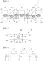
- FIG. 4 is a block diagram illustrating main components of a variable gain amplifier according to a second embodiment of the present invention.
- a variable gain amplifier 2 includes the input matching circuit 11, the output matching circuit 12, differential amplifier circuits 13-1 and 13-2, the variable attenuation circuit 14 (first variable attenuation circuit), a variable attenuation circuit 15 (second variable attenuation circuit), and an inter-stage matching circuit 16.
- the variable gain amplifier 1 of the first embodiment has a one-stage configuration in which only one differential amplifier circuit is provided in the propagation direction of the high-frequency signal.
- the variable gain amplifier 2 of the present embodiment has a two-stage configuration in which two differential amplifier circuits are provided in the propagation direction of the high-frequency signal.
- the variable gain amplifier 2 amplifies the high-frequency signals which are input from the pair of input terminals T11 and T12 and outputs the amplified signals from the pair of output terminals T21 and T22.
- the amplification factor of the variable gain amplifier 2 can be changed by a control signal which is input from the outside.
- the input matching circuit 11 and the output matching circuit 12 have the same configuration as that shown in FIG. 1 .
- the differential amplifier circuits 13-1 and 13-2 have the same configuration as the differential amplifier circuit 13 shown in FIG. 1 .
- the differential amplifier circuits 13-1 and 13-2 amplify high-frequency signals which are input from the pair of input terminals a1 and a2 with a predetermined amplification factor and output the amplified signals from the pair of output terminals b1 and b2.
- the differential amplifier circuits 13-1 and 13-2 may have a configuration, for example, as shown in FIG. 2 .
- the amplification factors of the differential amplifier circuits 13-1 and 13-2 can be arbitrarily set according to the application in which the variable gain amplifier 2 is used.
- the amplification factors of the differential amplifier circuits 13-1 and 13-2 may be the same as or different from each other.
- the differential amplifier circuits 13-1 and 13-2 are cascade-connected to each other in the propagation direction of the high-frequency signal with the inter-stage matching circuit 16 interposed therebetween. Specifically, the pair of input terminals a1 and a2 of the differential amplifier circuit 13-1 are connected to the output side of the input matching circuit 11, and the pair of output terminals b1 and b2 thereof are connected to the input side of the inter-stage matching circuit 16. The pair of input terminals a1 and a2 of the differential amplifier circuit 13-2 are connected to the output side of the inter-stage matching circuit 16, and the pair of output terminals b1 and b2 thereof are connected to the input side of the output matching circuit 12.
- variable attenuation circuit 14 A positional relationship between the variable attenuation circuit 14 and the differential amplifier circuit 13-2 is the same as that shown in FIG. 1 .
- the variable attenuation circuit 15 is connected between the pair of output terminals b1 and b2 of the differential amplifier circuit 13-1.
- the variable attenuation circuit 15 is a circuit which switches a resistance value between the pair of output terminals b1 and b2 of the differential amplifier circuit 13-1 on the basis of a control signal (not shown) which is input from the outside.
- the variable attenuation circuit 15 includes two ports P1 and P2.
- the port P1 is connected to the output terminal b1 of the differential amplifier circuit 13-1, and the port P2 is connected to the output terminal b2 of the differential amplifier circuit 13-1.
- the variable attenuation circuit 15 is provided to improve the frequency characteristics of the variable gain amplifier 2 by adjusting the resistance value between the output terminals b1 and b2 of the differential amplifier circuit 13-1.
- the variable attenuation circuit 15 may have the same configuration as or a different configuration from the variable attenuation circuit 14.
- the variable attenuation circuit 15 may have a configuration, for example, as shown in any one of FIGS. 3A to 3D .
- the inter-stage matching circuit 16 is a circuit that performs impedance matching between a first-stage amplifier circuit including the differential amplifier circuit 13-1 and a second-stage amplifier circuit including the differential amplifier circuit 13-2. Any circuit can be used as the inter-stage matching circuit 16 insofar as it can perform impedance matching between the first-stage amplifier circuit and the second-stage amplifier circuit.
- FIG. 5 is a circuit diagram illustrating a configuration example of the inter-stage matching circuit in the second embodiment of the present invention.
- the inter-stage matching circuit 16 includes a transformer 40 and capacitors 41 to 44, and constitutes a transformer coupling type double-tuned circuit.
- the transformer 40 includes a primary winding 40a and a secondary winding 40b.
- the primary winding 40a of the transformer 40 is connected between input terminals T31 and T32 of the inter-stage matching circuit 16, and the secondary winding 40b of the transformer 40 is connected between output terminals T41 and T42 of the inter-stage matching circuit 16.
- the capacitor 41 is connected between one end of the primary winding 40a, the input terminal T31, and the ground, and the capacitor 42 is connected between the other end of the primary winding 40a, the input terminal T32, and the ground.
- the capacitor 43 is connected between one end of the secondary winding 40b, the output terminal T41, and the ground, and the capacitor 44 is connected between the other end of the secondary winding 40b, the output terminal T42, and the ground.
- FIG. 6 is an equivalent half circuit of the variable gain amplifier according to the second embodiment of the present invention. Specifically, FIG. 6 is a half circuit including the output impedance of the differential amplifier circuit 13-1, the variable attenuation circuit 15, the inter-stage matching circuit 16, the variable attenuation circuit 14, and the input impedance of the differential amplifier circuit 13-2 which are shown in FIG. 4 .
- the reason why the frequency characteristics of the variable gain amplifier 2 is improved by providing the variable attenuation circuit 15 will be described with reference to the equivalent half circuit shown in FIG. 6 .
- L 1 is a primary-side inductance of the transformer 40 included in the inter-stage matching circuit 16
- L 2 is a secondary-side inductance of the transformer 40 included in the inter-stage matching circuit 16.
- M is an excitation inductance of the transformer 40.
- C 1 is a combined capacitance of the capacitance of the primary-side capacitor (for example, the capacitor 41) included in the inter-stage matching circuit 16 and the parasitic capacitance of the transistor (not shown) included in the differential amplifier circuit 13-1.
- C 2 is a combined capacitance of the capacitance of the secondary-side capacitor (for example, the capacitor 43) included in the inter-stage matching circuit 16 and the parasitic capacitance of the transistor (not shown) included in the differential amplifier circuit 13-2.
- R 1 is a combined resistance of the output impedance of the transistor (not shown) included in the differential amplifier circuit 13-1 and the equivalent resistance of the variable attenuation circuit 15.
- R 2 is a combined resistance of the input impedance of the transistor (not shown) included in the differential amplifier circuit 13-2 and the equivalent resistance of the variable attenuation circuit 14.
- variable gain amplifier 2 shown in FIG. 4
- switching the variable attenuation circuit 15 between an on state and an off state is equivalent to dynamically changing the combined resistance R 1 .
- switching the variable attenuation circuit 14 between an on state and an off state is equivalent to dynamically changing the combined resistance R 2 .
- the combined resistance R 1 is a combined resistance of the output impedance of the transistor (not shown) included in the differential amplifier circuit 13-1 and the equivalent resistance of the variable attenuation circuit 15.
- the combined resistance R 2 is a combined resistance of the input impedance of the transistor (not shown) included in the differential amplifier circuit 13-2 and the equivalent resistance of the variable attenuation circuit 14. Therefore, the magnitude of the high-frequency signal that actually acts on each transistor is a value distributed according to the ratio of the impedance of each transistor to the magnitude of each equivalent resistance.
- the distribution ratio is assumed to have no frequency characteristics in order not to influence the following discussion, the combined resistance R 1 is treated as a source impedance of the equivalent half circuit, and the combined resistance R 2 is treated as a load impedance thereof.
- a double-tuned circuit is configured by coupling two resonance circuits.
- the inter-stage matching circuit 16 shown in FIG. 6 constitutes a transformer coupling type double-tuned circuit.
- a resonance circuit formed of the capacitance C 1 and the inductance L 1 and a resonance circuit formed of the capacitance C 2 and the inductance L 2 are coupled to each other by using the excitation inductance M.
- FIG. 6 shows a transformer coupling type double-tuned circuit, it may be a capacitive coupling type double-tuned circuit.
- the resonance circuit shown in FIG. 6 is a parallel resonance circuit, it may be a series resonance circuit.
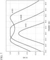
- FIG. 7 is a diagram illustrating pass characteristics of the equivalent half circuit shown in FIG. 6 .
- the pass characteristics shown in FIG. 7 are calculated with the combined resistances R 1 and R 2 set to 50 [ ⁇ ], the capacitance C 1 and C 2 set to 400 [fF], and the inductance Li, L 2 set to 80 [pH] in the equivalent half circuit shown in FIG. 6 .
- FIG. 7 shows pass characteristics when the coupling coefficient k is set to 0.1, pass characteristics when the coupling coefficient k is set to 0.28, and pass characteristics when the coupling coefficient k is set to 0.5.
- Equation (3) x in the following Equation (3) is a variable that may be 1 or 2. That is, L x in the following Equation (3) is L 1 or L 2 , and R x is R 1 or R 2 .
- the center frequency f 0 is generally designed to match the driving frequency of the variable gain amplifier 2.
- Z 1 , Z 2 , and Z 3 are impedances when the equivalent half circuit is viewed from points A, B, and C in the drawing, respectively, in the propagation direction of the high-frequency signal.
- the impedance Z 3 is impedance when the differential amplifier circuit 13-2 is viewed from the combined resistance R 1 .
- the impedances Z 1 , Z 2 , and Z 3 are expressed by the following Equations (4) to (6), respectively.
- the inductance L 1 is designed to be larger than the inductance L 2 in order to match the value Q L of the load Q in the primary-side and secondary-side resonance circuits. Therefore, it is preferable that the equivalent resistance of the variable attenuation circuit 15 be larger than the equivalent resistance of the variable attenuation circuit 14.
- the equivalent resistances of the variable attenuation circuits 15 and 14 have a plurality of levels, it is preferable that the plurality of levels change at the same ratio.
- the ratio of the equivalent resistance of the variable attenuation circuit 15 to the equivalent resistance of the variable attenuation circuit 14 at each of these levels be equal to the ratio of the primary-side inductance to the secondary-side inductance.
- variable attenuation circuits 15 and 14 are switched between an on state and off state, the combined resistances R 1 and R 2 change dynamically, and thus the value Q L of the load Q in each resonance circuit also changes dynamically. Consequently, numerical calculations were performed to confirm how the pass characteristics change depending on the mode of change in the value Q L of the load Q in each resonance circuit.
- FIGS. 8A and 8B are diagrams illustrating pass characteristics in a case where the combined resistance R 2 is changed in the equivalent half circuit shown in FIG. 6 .
- the pass characteristics shown in FIGS. 8A and 8B are calculated with the combined resistances R 1 and R 2 set to 50 [ ⁇ ], the capacitances C 1 and C 2 set to 400 [fF], the inductances L 1 and L 2 set to 80 [pH], and the coupling coefficient k set to 0.28.
- FIG. 8A illustrates pass characteristics of the equivalent half circuit in a case where the value of the combined resistance R 1 is fixed at 50 [ ⁇ ] and the combined resistance R 2 is changed from 50 [ ⁇ ] to 20 [ ⁇ ].
- FIG. 8B illustrates pass characteristics of the equivalent half circuit in a case where the value of the combined resistance R 1 is made to follow the combined resistance R 2 while the combined resistance R 2 is changed from 50 [ ⁇ ] to 20 [ ⁇ ].
- variable attenuation circuit 15 and the variable attenuation circuit 14 are operated simultaneously, the frequency characteristics are better and the amount of attenuation is larger than in a case where only the variable attenuation circuit 14 is operated, and thus it can be said that the attenuation circuit exhibits good characteristics. That is, in the case of a two-stage configuration in which two differential amplifier circuits 13-1 and 13-2 are provided in the propagation direction of the high-frequency signal as in the variable gain amplifier 2 of the present embodiment, it is preferable to include the variable attenuation circuit 15 in addition to the variable attenuation circuit 14.
- the differential amplifier circuit 13-1 is provided between the input matching circuit 11 and the inter-stage matching circuit 16, and the differential amplifier circuit 13-2 is provided between the inter-stage matching circuit 16 and the output matching circuit 12.
- the variable attenuation circuit 14 is connected between the pair of input terminals a1 and a2 of the differential amplifier circuit 13-2
- the variable attenuation circuit 15 is connected between the pair of output terminals b1 and b2 of the differential amplifier circuit 13-1.
- the resistance values of the variable attenuation circuits 14 and 15 are switched on the basis of control signals which are input from the outside. Thereby, it is possible to achieve a reduction in size and to suppress loss due to impedance mismatching. Additionally, since the frequency characteristics are good and the amount of attenuation can be made larger, it is possible to realize good characteristics as an attenuation circuit.
- FIGS. 9A and 9B are block diagrams illustrating modification examples of the variable gain amplifier according to the second embodiment of the present invention.
- the input matching circuit 11 and the output matching circuit 12 are not shown.
- a variable gain amplifier 2A shown in FIG. 9A includes four differential amplifier circuits 13-1 to 13-4 which are cascade-connected to each other and three variable attenuation circuits 14-1 to 14-3 (first variable attenuation circuits) connected between the input terminals of the differential amplifier circuits 13-2 to 13-4, respectively.
- variable attenuation circuits 15-1 to 15-3 (second variable attenuation circuits) connected between the output terminals of the differential amplifier circuits 13-1 to 13-3, respectively, to the variable gain amplifier 2A shown in FIG. 9A .
- variable gain amplifiers 2A and 2B shown in FIGS. 9A and 9B have a four-stage configuration in which the four differential amplifier circuits 13-1 to 13-4 are provided, and are configured with the variable attenuation circuits 14-1 to 14-3 connected between the input terminals of the differential amplifier circuits 13-2 to 13-4 in the second to fourth stages, respectively.
- variable gain amplifier 2A shown in FIG. 9A a variable attenuation circuit connected between the output terminals of the differential amplifier circuit is omitted, but in the variable gain amplifier 2B shown in FIG. 9B , the variable attenuation circuits 15-1 to 15-3 are connected between the output terminals of the differential amplifier circuits 13-1 to 13-3 in the first to third stages, respectively.
- inter-stage matching circuits 16-1 to 16-3 are provided at the preceding stage of the variable attenuation circuit 14-1 to 14-3, respectively.
- the inter-stage matching circuits 16-1 to 16-3 are provided between the variable attenuation circuits 14-1 and 15-1, between the variable attenuation circuits 14-2 and 15-2, and between the variable attenuation circuits 14-3 and 15-3, respectively.
- variable gain amplifier includes N (N is an integer equal to or greater than 2) differential amplifier circuits which are cascade-connected to each other
- N is an integer equal to or greater than 2
- variable attenuation circuits are connected between the input terminals of the differential amplifier circuits in the second to nth stage along the propagation direction of the high-frequency signal
- FIG. 9B a configuration in which variable attenuation circuits are connected between the output terminals of the differential amplifier circuits in the first to (N-1)th stages may be adopted (see FIG. 9B ).
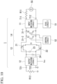
- FIG. 10 is a diagram illustrating a variable gain amplifier according to a first example.
- the present example is an example of the variable gain amplifier 1 according to the first embodiment.
- components corresponding to the components shown in FIGS. 1 to 3D are denoted by the same reference numerals and signs.
- the variable gain amplifier 1 includes a bias circuit 51 and a control circuit 52 in addition to the input matching circuit 11, the output matching circuit 12, the differential amplifier circuit 13, and the variable attenuation circuit 14.
- the differential amplifier circuit 13 includes the two transistors 21 and 22 shown in FIG. 2 and two neutralization capacitors 23 and 24.
- the neutralization capacitor 23 is connected between the base terminal of the transistor 21 and the collector terminal of the transistor 22, and the neutralization capacitor 24 is connected between the base terminal of the transistor 22 and the collector terminal of the transistor 21.
- the variable attenuation circuit 14 includes the two transistors 31-1 and 31-2 connected in parallel to each other as shown in FIG. 3C .
- the transistors 31-1 and 31-2 are N-type MOSFETs.
- the sizes of the transistor 31-1 (second FET) and the transistor 31-2 (first FET) are as shown in the following Table 1. [Table 1] Gate length Gate width First FET 240nm 45 ⁇ m Second FET 240nm 90pm
- a power supply voltage Vcc is supplied to the output matching circuit 12.
- the power supply voltage Vcc is applied to the collector terminals of the transistors 21 and 22 provided in the differential amplifier circuit 13 via the output matching circuit 12.
- the bias circuit 51 is connected to the input matching circuit 11.
- the bias circuit 51 outputs a bias current which is to be supplied to the base terminals of the transistors 21 and 22 provided in the differential amplifier circuit 13.
- the bias current which is output from the bias circuit 51 is supplied to the base terminals of the transistors 21 and 22 via the input matching circuit 11.
- the control circuit 52 individually controls an on state or an off state of the two transistors 31-1 and 31-2 provided in the variable attenuation circuit 14.
- a series circuit of a high-frequency signal source SG and a resistor R11 is connected between the input terminals T11 and T12 of the variable gain amplifier 1, and a resistor R12 is connected between the output terminals T21 and T22 of the variable gain amplifier 1.
- the output terminal T22 is connected to the ground.
- the resistance value of the resistor R11 is, for example, 100 [ ⁇ ]
- the resistance value of the resistor R12 is, for example, 50 [ ⁇ ].
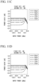
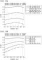
- FIGS. 11A to 11D are diagrams illustrating power gains of the variable gain amplifier according to the first example. Specifically, FIGS. 11A to 11D illustrate power gains at a frequency of 28 [GHz] when the bias current which is output from the bias circuit 51 is set to 22, 31, 42, 54, and 61 [ ⁇ A] and the input power to the input terminals T11 and T12 is changed.
- FIG. 11A shows a case where both the transistor 31-2 (first FET) and the transistor 31-1 (second FET) of the variable attenuation circuit 14 are set to be in an off state.
- FIG. 11B shows a case where the transistor 31-2 (first FET) of the variable attenuation circuit 14 is set to be in an on state and the transistor 31-1 (second FET) thereof is set to be in an off state.
- FIG. 11C shows a case where the transistor 31-2 (first FET) of the variable attenuation circuit 14 is set to be in an off state and the transistor 31-1 (second FET) thereof is set to be in an on state.
- FIG. 11D shows a case where both the transistor 31-2 (first FET) and the transistor 31-1 (second FET) of the variable attenuation circuit 14 are set to be in an on state.
- the power gain can be lowered without deteriorating the linearity by setting at least one of the transistor 31-2 (first FET) and the transistor 31-1 (second FET) provided in the variable attenuation circuit 14 to be in an on state (for example, it is clear when comparing the power gain of 3.0 dB (bias current of 31 ⁇ A) in the graph shown in FIG. 11A with the power gain of 3.0 dB (bias current of 64 ⁇ A) in the graph shown in FIG. 11B ).
- the power gain can be lowered stepwise by changing a combination of the on state and off state of the transistor 31-2 (first FET) and the transistor 31-1 (second FET).
- FIG. 12 is a diagram illustrating a variable gain amplifier according to a second example.
- the present example is an example of the variable gain amplifier 2 according to the second embodiment.
- components corresponding to the components shown in FIGS. 2 to 5 are denoted by the same reference numerals and signs.
- the variable gain amplifier 2 includes bias circuits 51 and 53 and a control circuit 54 in addition to the input matching circuit 11, the output matching circuit 12, the differential amplifier circuits 13-1 and 13-2, the variable attenuation circuits 14 and 15, and the inter-stage matching circuit 16.
- the differential amplifier circuits 13-1 and 13-2 include the two transistors 21 and 22 and the two neutralization capacitors 23 and 24 similarly to the differential amplifier circuit 13 shown in FIG. 10 .
- the variable attenuation circuits 14 and 15 include the two transistors 31-1 and 31-2 connected in parallel to each other similarly to the variable attenuation circuit 14 shown in FIG. 10 .
- the transistors 31-1 and 31-2 are N-type MOSFETs.
- the sizes of the transistor 31-1 (second FET) and the transistor 31-2 (first FET) provided in the variable attenuation circuit 15 and the transistor 31-1 (fourth FET) and the transistor 31-2 (third FET) provided in the variable attenuation circuit 14 are as shown in the following Table 2. [Table 2] Gate length Gate width First FET 240nm 7.5 ⁇ m Second FET 240nm 15 ⁇ m Third FET 240nm 45pm Fourth FET 240nm 90 ⁇ m
- the gate widths of the transistors (first and second FETs) of the variable attenuation circuit 15 are different from each other, and the gate width of the transistors (third and fourth FETs) of the variable attenuation circuit 14 are different from each other.
- a power supply voltage Vcc is supplied to the output matching circuit 12 and the inter-stage matching circuit 16.
- the power supply voltage Vcc is applied to the collector terminals of the transistors 21 and 22 provided in the differential amplifier circuit 13-2 via the output matching circuit 12.
- the power supply voltage Vcc is applied to the collector terminals of the transistors 21 and 22 provided in the differential amplifier circuit 13-1 via the middle point of the primary winding 40a of the transformer 40 provided in the inter-stage matching circuit 16.
- the bias circuit 51 is connected to the input matching circuit 11, and the bias circuit 53 is connected to the inter-stage matching circuit 16.
- the bias circuit 51 outputs a bias current which is to be supplied to the base terminals of the transistors 21 and 22 provided in the differential amplifier circuit 13-1.
- the bias circuit 53 outputs a bias current which is to be supplied to the base terminals of the transistors 21 and 22 provided in the differential amplifier circuit 13-2.
- the bias current which is output from the bias circuit 51 is supplied to the base terminals of the transistors 21 and 22 provided in the differential amplifier circuit 13-1 via the input matching circuit 11.
- the bias current which is output from the bias circuit 53 is supplied to the base terminals of the transistors 21 and 22 provided in the differential amplifier circuit 13-2 via the middle point of the secondary winding 40b of the transformer 40 provided in the inter-stage matching circuit 16.
- the control circuit 54 individually controls an on state or an off state of the transistors 31-1 and 31-2 provided in the variable attenuation circuits 14 and 15.
- the series circuit of the high-frequency signal source SG and the resistor R11 is connected between the input terminals T11 and T12 of the variable gain amplifier 2, and the resistor R12 is connected between the output terminals T21 and T22 of the variable gain amplifier 2.
- the output terminal T22 is connected to the ground.
- the resistance value of the resistor R11 is, for example, 100 [ ⁇ ]
- the resistance value of the resistor R12 is, for example, 50 [ ⁇ ]. This is the same as in the first example.
- FIGS. 13A and 13B are diagrams illustrating frequency characteristics of pass characteristics of the variable gain amplifier according to the second example.
- FIG. 13A illustrates frequency characteristics of pass characteristics of the variable gain amplifier 2 in a case where a combination of the on state and off state of the transistors 31-1 and 31-2 provided in the variable attenuation circuits 14 and 15 is changed.
- FIG. 13B illustrates frequency characteristics of pass characteristics of the variable gain amplifier 2 in a case where a combination of the on state and off state of the transistors 31-1 and 31-2 provided in the variable attenuation circuit 14 is changed with the exception of the variable attenuation circuit 15.
- the first FET shown in FIGS. 13A and 13B is the transistor 31-2 provided in the variable attenuation circuit 15, and the second FET is the transistor 31-1 provided in the variable attenuation circuit 15.
- the third FET is the transistor 31-2 provided in the variable attenuation circuit 14
- the fourth FET is the transistor 31-1 provided in the variable attenuation circuit 14.
- the graph shown in FIG. 13A has a larger amount of attenuation and a smaller inclination than the graph shown in FIG. 13B . That is, it can be understood that the frequency characteristics can be improved in a case where the variable attenuation circuit 15 is provided in the variable gain amplifier 2 more than in a case where the variable attenuation circuit 15 is not provided therein.
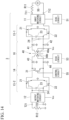
- FIG. 14 is a diagram illustrating a variable gain amplifier according to a third example.
- a variable gain amplifier 3 according to the present example has a configuration in which the configuration of the variable attenuation circuit 14 of the variable gain amplifier 2 shown in FIG. 12 is simplified, the variable attenuation circuit 15 is omitted, and a control circuit 55 is provided instead of the control circuit 54 shown in FIG. 12 .
- components corresponding to the components shown in FIGS. 12 and 3A are denoted by the same reference numerals and signs. In addition, the same components as those shown in FIG. 12 will be omitted.
- the variable attenuation circuit 14 includes the transistor 31 shown in FIG. 3A .
- the transistor 31 is an N-type MOSFET.
- FET field-effect transistor
- Table 3 Gate length Gate width Equivalent resistance FET 240nm 150 ⁇ m 7.62 ⁇
- the control circuit 55 controls an on state or an off state of the transistor 31 provided in the variable attenuation circuit 14.
- the series circuit of the high-frequency signal source SG and the resistor R11 is connected between the input terminals T11 and T12 of the variable gain amplifier 3, and the resistor R12 is connected between the output terminals T21 and T22 of the variable gain amplifier 3.
- the output terminal T22 is connected to the ground.
- the resistance value of the resistor R11 is, for example, 100 [ ⁇ ]
- the resistance value of the resistor R12 is, for example, 50 [ ⁇ ]. This is the same as in the first and second examples.
- Table 4 indicates power gains of the variable gain amplifier according to the third example. Specifically, Table 4 indicates the power gains at a frequency of 28 [GHz] when the temperature is set to -40, 65, and 125 [°C]. Table 4 shows power gains in a case where the transistor 31 (FET) of the variable gain amplifier 3 is set to be in an on state, a case where the transistor 31 (FET) of the variable gain amplifier 3 is replaced with an ideal resistor, and a case where the variable attenuation circuit 14 is removed from the variable gain amplifier 3.
- the resistance value of the ideal resistor is the resistance value of the equivalent resistance shown in Table 3 (7.62 [Q]).
- a fluctuation in the power gain when the temperature changes from -40 [°C] to 125 [°C] is as follows in each of the cases.
- the fluctuation is 4.9 [dB] in a case where the transistor 31 (FET) of the variable gain amplifier 3 is set to be in an on state.
- the fluctuation is 7.5 [dB] in a case where the transistor 31 (FET) of the variable gain amplifier 3 is replaced with the ideal resistance.
- the fluctuation is 7.1 [dB] in a case where the variable attenuation circuit 14 is removed from the variable gain amplifier 3.
- the present invention is not limited to the embodiments and examples, and can be freely changed within the scope of the present invention.
- the power gain at a frequency of 28 [GHz] has been stated in the above-described examples, the present invention can cope with, for example, high-frequency signals having any frequencies in a microwave band or a millimeter wave band.
Landscapes
- Engineering & Computer Science (AREA)
- Power Engineering (AREA)
- Multimedia (AREA)
- Amplifiers (AREA)
- Networks Using Active Elements (AREA)
- Control Of Amplification And Gain Control (AREA)
Abstract
Description
- The present invention relates to a variable gain amplifier.
- In recent years, wireless communication using high-frequency signals of microwaves, millimeter waves, or the like has been in the spotlight. In wireless communication devices that transmit and receive such high-frequency signals, it may be necessary to adjust the level of a transmission signal or a received signal. Variable gain amplifiers are provided in wireless communication devices, for example, in order to perform such power adjustment.
- Satoshi Tanaka, "Progress of the linear RF power amplifier for mobile phones," IEICE Trans. Fundamentals, vol. E101-A, No. 2 pp. 385-395, 2018 (hereinafter referred to as Non-Patent Document 1) discloses a two-stage power amplifier in which an amplifier circuit constituted by a transistor and a bias circuit is provided between an input matching circuit and an inter-stage matching circuit, and between the inter-stage matching circuit and an output matching circuit. In addition,
Japanese Unexamined Patent Application, First Publication No. 2008-48455 Document 1 and the attenuator disclosed inPatent Document 1. - In a configuration in which either the power amplifier of
Non-Patent Document 1 or the attenuator ofPatent Document 1 is switchably connected to a high-frequency signal path, a plurality of paths are required, which makes it difficult to achieve a reduction in size. In addition, in such a configuration, a switching circuit including a field-effect transistor (FET) or the like is required to be connected in series to the high-frequency signal path, resulting in impedance mismatching and an increase in loss. - The present invention has been made in view of the above-described circumstances and an object thereof is to provide a variable gain amplifier that makes it possible to achieve a reduction in size and suppress loss due to impedance mismatching.
- A variable gain amplifier according to a first aspect of the present invention includes a differential amplifier circuit having a pair of input terminals and a pair of output terminal, and a first variable attenuation circuit connected between at least one of the pair of input terminals and the pair of output terminals of the differential amplifier circuit and capable of switching a resistance value on the basis of a control signal which is input from the outside.
- In the variable gain amplifier according to the first aspect of the present invention, the first variable attenuation circuit is connected between at least one of the pair of input terminals and the pair of output terminals of the differential amplifier circuit that amplifies a high-frequency signal, and the resistance value between the at least one of the pair of input terminals and the pair of output terminals can be switched on the basis of the control signal which is input from the outside. This eliminates the need to switchably connect an attenuator to a high-frequency signal path as in the related art, and thus it is possible to achieve a reduction in size. In addition, since there is no need to connect a switching circuit including a field-effect transistor (FET) or the like in series to the high-frequency signal path, it is possible to suppress loss due to impedance mismatching.
- According to a second aspect of the present invention, in the variable gain amplifier according to the first aspect of the present invention, the differential amplifier circuit may include N (N is an integer equal to or greater than 2) differential amplifier circuits cascade-connected to each other in a propagation direction of a high-frequency signal, and the first variable attenuation circuit may be connected between the pair of input terminals of at least one of the differential amplifier circuits in second to nth stages counted from the pair of input terminals of the variable gain amplifier.
- According to a third aspect of the present invention, the variable gain amplifier according to the second aspect of the present invention may further include a second variable attenuation circuit connected between the pair of output terminals of the differential amplifier circuit at a preceding stage of the differential amplifier circuit including the pair of input terminals to which the first variable attenuation circuit is connected, and capable of switching a resistance value between the pair of output terminals on the basis of a control signal which is input from the outside.
- According to a fourth aspect of the present invention, in the variable gain amplifier according to any one of the first to third aspects of the present invention, the first variable attenuation circuit may include a transistor connected between the pair of input terminals.
- According to a fifth aspect of the present invention, in the variable gain amplifier according to the fourth aspect of the present invention, the first variable attenuation circuit may include a resistor connected in series or in parallel to the transistor.
- According to a sixth aspect of the present invention, in the variable gain amplifier according to the fourth or fifth aspect of the present invention, the transistor may be controlled to be in an on state or an off state on the basis of the control signal.
- According to a seventh aspect of the present invention, in the variable gain amplifier according to the fourth or fifth aspect of the present invention, the first variable attenuation circuit may include a plurality of the transistors, and the plurality of transistors may be individually controlled to be in an on state or an off state on the basis of a plurality of the control signals.
- According to an eighth aspect of the present invention, in the variable gain amplifier according to the fourth or fifth aspect of the present invention, the first variable attenuation circuit may further include a bias circuit configured to adjust a resistance value of the transistor by changing a bias voltage applied to the transistor on the basis of a plurality of control signals which are input from the outside.
- According to a ninth aspect of the present invention, in the variable gain amplifier according to the third aspect of the present invention, the second variable attenuation circuit may include a transistor connected between the pair of output terminals.
- According to a tenth aspect of the present invention, in the variable gain amplifier according to the ninth aspect of the present invention, the second variable attenuation circuit may include a resistor connected in series or in parallel to the transistor.
- According to an eleventh aspect of the present invention, in the variable gain amplifier according to the ninth or tenth aspect of the present invention, the transistor may be controlled to be in an on state or an off state on the basis of the control signal.
- According to a twelfth aspect of the present invention, in the variable gain amplifier according to the ninth or tenth aspect of the present invention, the second variable attenuation circuit may include a plurality of the transistors, and the plurality of transistors may be individually controlled to be in an on state or an off state on the basis of a plurality of the control signals.
- According to a thirteenth aspect of the present invention, in the variable gain amplifier according to the ninth or tenth aspect of the present invention, the second variable attenuation circuit may further include a bias circuit configured to adjust a resistance value of the transistor by changing a bias voltage applied to the transistor on the basis of a plurality of control signals which are input from the outside.
- According to a fourteenth aspect of the present invention, in the variable gain amplifier according to the third aspect of the present invention, the first variable attenuation circuit may include a plurality of transistors connected between the pair of input terminals, the second variable attenuation circuit may include a plurality of transistors connected between the pair of output terminals, gate widths of the plurality of transistors of the first variable attenuation circuit may be different from each other, gate widths of the plurality of transistors of the second variable attenuation circuit may be different from each other, and in a case where the plurality of transistors of the first variable attenuation circuit are lined up in ascending order of gate width and the plurality of transistors of the second variable attenuation circuit are lined up in ascending order of gate width, ratios of gate widths of the transistors in the same place may be the same as each other.
- According to the present invention, it is possible to achieve a reduction in size and to suppress loss due to impedance mismatching.
-
-
FIG. 1 is a block diagram illustrating main components of a variable gain amplifier according to a first embodiment of the present invention. -
FIG. 2 is a circuit diagram illustrating a configuration example of a differential amplifier circuit according to the first embodiment of the present invention. -
FIGS. 3A to 3D are circuit diagrams illustrating configuration examples of a variable attenuation circuit according to the first embodiment of the present invention. -
FIG. 4 is a block diagram illustrating main components of a variable gain amplifier according to a second embodiment of the present invention. -
FIG. 5 is a circuit diagram illustrating a configuration example of an inter-stage matching circuit according to the second embodiment of the present invention. -
FIG. 6 is an equivalent half circuit of the variable gain amplifier according to the second embodiment of the present invention. -
FIG. 7 is a diagram illustrating pass characteristics of the equivalent half circuit shown inFIG. 6 . -
FIGS. 8A and 8B are diagrams illustrating pass characteristics of the equivalent half circuit shown inFIG. 6 in a case where a combined resistance R2 is changed. -
FIGS. 9A and9B are block diagrams illustrating modification examples of the variable gain amplifier according to the second embodiment of the present invention. -
FIG. 10 is a diagram illustrating a variable gain amplifier according to a first example. -
FIGS. 11A to 11D are diagrams illustrating power gains of the variable gain amplifier according to the first example. -
FIG. 12 is a diagram illustrating a variable gain amplifier according to a second example. -
FIGS. 13A and 13B are diagrams illustrating frequency characteristics of pass characteristics of the variable gain amplifier according to the second example. -
FIG. 14 is a diagram illustrating a variable gain amplifier according to a third example. - Hereinafter, variable gain amplifiers according to embodiments of the present invention will be described in detail with reference to the accompanying drawings.
-
FIG. 1 is a block diagram illustrating main components of a variable gain amplifier according to a first embodiment of the present invention. As shown inFIG. 1 , avariable gain amplifier 1 according to the present embodiment includes aninput matching circuit 11, anoutput matching circuit 12, adifferential amplifier circuit 13, and a variable attenuation circuit 14 (first variable attenuation circuit). Thevariable gain amplifier 1 amplifies a high-frequency signal which is input from a pair of input terminals T11 and T12 and outputs the amplified signal from a pair of output terminals T21 and T22. Although the details will be described later, the amplification factor of thevariable gain amplifier 1 can be changed by a control signal which is input from the outside. - Hereinafter, for convenience of description, an upper line (a line to which the input terminal T11, the output terminal T21, and the like are connected) in
FIG. 1 and elements connected to the upper line are referred to as a "p side" in some cases. In addition, a lower line (a line to which the input terminal T12, the output terminal T22, and the like are connected) inFIG. 1 and elements connected to the lower line are referred to as an "n side" in some cases. A high-frequency signal which is input to thevariable gain amplifier 1 is, for example, a signal of microwaves (3 to 30 [GHz]) or millimeter waves (30 to 300 [GHz]). - The
input matching circuit 11 is a circuit that performs impedance matching on the input side of the variable gain amplifier 1 (that is, on a side of the pair of input terminals T11 and T12). Theoutput matching circuit 12 is a circuit that performs impedance matching on the output side of the variable gain amplifier 1 (that is, on a side of the pair of output terminals T21 and T22). Although a case where a signal which is input and output to and from thevariable gain amplifier 1 is a balanced signal will be described as an example in the present embodiment, the signal which is input and output to and from thevariable gain amplifier 1 may be an unbalanced signal. - In a case where the signal which is input and output to and from the
variable gain amplifier 1 is an unbalanced signal, theinput matching circuit 11 is provided with a conversion circuit (balun) that converts the unbalanced signal into a balanced signal, and theoutput matching circuit 12 is provided with a conversion circuit (balun) that converts the balanced signal into an unbalanced signal. In this case, either the p side or the n side is connected to the ground. - The
differential amplifier circuit 13 includes a pair of input terminals a1 and a2 and a pair of output terminals b1 and b2. Thedifferential amplifier circuit 13 amplifies high-frequency signals which are input from the pair of input terminals a1 and a2 with a predetermined amplification factor and outputs the amplified signals from the pair of output terminals b1 and b2. The pair of input terminals a1 and a2 of thedifferential amplifier circuit 13 are connected to the output sides of theinput matching circuit 11, and the pair of output terminals b1 and b2 of thedifferential amplifier circuit 13 are connected to the input sides of theoutput matching circuit 12. The amplification factor of thedifferential amplifier circuit 13 can be arbitrarily set according to the application in which thevariable gain amplifier 1 is used. -
FIG. 2 is a circuit diagram illustrating a configuration example of a differential amplifier circuit according to the first embodiment of the present invention. As shown inFIG. 2 , thedifferential amplifier circuit 13 includes a p-side transistor 21 and an n-side transistor 22. InFIG. 2 , for the purpose of simplifying the description, only thetransistors transistors - As shown in
FIG. 2 , thetransistors transistor 21 is connected to the input terminal a1 of thedifferential amplifier circuit 13, the collector terminal thereof is connected to the output terminal b1 of thedifferential amplifier circuit 13, and the emitter terminal thereof is connected to the ground. The base terminal of thetransistor 22 is connected to the input terminal a2 of thedifferential amplifier circuit 13, the collector terminal thereof is connected to the output terminal b2 of thedifferential amplifier circuit 13, and the emitter terminal thereof is connected to the ground. - A neutralization capacitor may be provided between the base terminal of the
transistor 21 and the collector terminal of thetransistor 22, and between the base terminal of thetransistor 22 and the collector terminal of thetransistor 21. By providing the neutralization capacitor, it is possible to improve isolation between the input side and the output side of thedifferential amplifier circuit 13. AlthoughFIG. 2 shows an example in which thetransistors transistors - The
variable attenuation circuit 14 is connected between the pair of input terminals a1 and a2 of thedifferential amplifier circuit 13. Thevariable attenuation circuit 14 is a circuit which switches a resistance value between the pair of input terminals a1 and a2 of thedifferential amplifier circuit 13 on the basis of a control signal (not shown) which is input from the outside. Thevariable attenuation circuit 14 includes two ports P1 and P2. The port P1 is connected to the input terminal a1 of thedifferential amplifier circuit 13, and the port P2 is connected to the input terminal a2 of thedifferential amplifier circuit 13. - The
variable attenuation circuit 14 is provided to control the amount of attenuation of a high-frequency signal which is input to thedifferential amplifier circuit 13. For example, in a case where the resistance value of thevariable attenuation circuit 14 is relatively large, the amount of attenuation of the high-frequency signal which is input to thedifferential amplifier circuit 13 can be made relatively small. On the contrary, in a case where the resistance value of thevariable attenuation circuit 14 is relatively small, the amount of attenuation of the high-frequency signal which is input to thedifferential amplifier circuit 13 can be made relatively large. - However, the
variable attenuation circuit 14 may be connected between the pair of output terminals b1 and b2 of thedifferential amplifier circuit 13. That is, the port P1 may be connected to the output terminal b1 of thedifferential amplifier circuit 13, and the port P2 may be connected to the output terminal b2 of thedifferential amplifier circuit 13. -
FIGS. 3A to 3D are circuit diagrams illustrating configuration examples of the variable attenuation circuit according to the first embodiment of the present invention. Thevariable attenuation circuit 14 illustrated inFIG. 3A includes atransistor 31. Thetransistor 31 is an N-type metal oxide film semiconductor field-effect transistor (MOSFET) having a gate terminal, a source terminal, and a drain terminal. The drain terminal of thetransistor 31 is connected to the port P1, and the source terminal thereof is connected to the port P2. In addition, the gate terminal of thetransistor 31 is connected to a control port C to which a control signal from the outside is input. - The
transistor 31 is controlled to be in an on state (electrical conduction state) or an off state (insulated state) on the basis of the control signal which is input to the control port C. In a case where thetransistor 31 is in an off state, the port P1 and the port P2 (the pair of input terminals a1 and a2 of the differential amplifier circuit 13) are electrically insulated from each other, and thus a high-frequency signal which is input to thevariable attenuation circuit 14 is not attenuated. On the other hand, when thetransistor 31 is in an on state, the on-resistance of thetransistor 31 establishes resistance connection between the port P1 and the port P2 (between the pair of input terminals a1 and a2 of the differential amplifier circuit 13), thereby attenuating the high-frequency signal which is input to thevariable attenuation circuit 14. In this manner, it is possible to control the amount of attenuation of the high-frequency signal which is input to thevariable attenuation circuit 14 on the basis of the control signal input to the control port C. - By providing the
variable attenuation circuit 14 illustrated inFIG. 3A , there is no need to switchably connect an attenuator to a high-frequency signal path as in the related art, and thus it is possible to achieve a reduction in size. In addition, since there is no need to connect a switching circuit including a field-effect transistor (FET) or the like in series to the high-frequency signal path, it is possible to suppress an increase in loss due to the occurrence of impedance mismatching. Further, in a case where the characteristics of thetransistor 31 change due to a change in temperature, the polarity of the temperature gradient of the amplification factor of thedifferential amplifier circuit 13 and the polarity of the temperature gradient of the on-resistance of thetransistor 31 included in thevariable attenuation circuit 14 coincide with each other. Therefore, an increase (or, decrease) in the amplification factor of thedifferential amplifier circuit 13 and an increase (or, decrease) in the signal attenuation factor caused by thevariable attenuation circuit 14 occur simultaneously, and thus the temperature change of the amplification factor of thedifferential amplifier circuit 13 is suppressed. That is, it is possible to improve the temperature characteristics of thevariable gain amplifier 1. - The
variable attenuation circuit 14 illustrated inFIG. 3B includes aresistor 32 in addition to thetransistor 31. Theresistor 32 is connected between the drain terminal of thetransistor 31 and the port P1. Theresistor 32 is provided to adjust the resistance value between the port P1 and the port P2 (between the pair of input terminals a1 and a2 of the differential amplifier circuit 13) when thetransistor 31 is in an on state to adjust the amount of attenuation of the high-frequency signal which is input to thevariable attenuation circuit 14. - The
resistor 32 may be connected between the source terminal of thetransistor 31 and the port P2. Alternatively, theresistor 32 may be connected in parallel to thetransistor 31. That is, theresistor 32 may be connected between the source terminal and the drain terminal of thetransistor 31. - The
variable attenuation circuit 14 illustrated inFIG. 3C includes a plurality of transistors 31-1 to 31-n (n is an integer equal to or greater than 2) connected in parallel to each other. The transistors 31-1 to 31-n are the same N-type MOSFETs as thetransistor 31 shown inFIGS. 3A and 3B . The drain terminals of the transistors 31-1 to 31-n are connected to the port P1, and the source terminals thereof are connected to the port P2. The gate terminals of the transistors 31-1 to 31-n are connected to control ports C1 to Cn, respectively. Control signals for individually controlling the on state or the off state of the transistors 31-1 to 31-n are input to the control ports C1 to Cn. - By individually controlling the on state or the off state of the transistors 31-1 to 31-n with the control signals which are input to the control ports C1 to Cn, the resistance value between the port P1 and the port P2 (between the pair of input terminals a1 and a2 of the differential amplifier circuit 13) can be switched stepwise. That is, the amount of attenuation of the high-frequency signal which is input to the
variable attenuation circuit 14 can be adjusted dynamically and stepwise by the control signals which are input to the control ports C1 to Cn. - Here, by making the sizes of the transistors 31-1 to 31-n different from each other, it is possible to efficiently increase the level of the amount of attenuation. Typically, in a case where the sizes of the transistors 31-1 to 31-n increase in this order, it is preferable that the size of the transistor 31-x (x is an integer that satisfies 1 ≤ x ≤ n) be 2(x-1) times the size of the smallest transistor 31-1. In this way, the amount of attenuation of the
variable attenuation circuit 14 can be changed so as to increase or decrease in binary numbers. - In the
variable attenuation circuit 14 illustrated inFIG. 3C , each of the transistors 31-1 to 31-n may be connected to theresistor 32 as in thetransistor 31 shown inFIG. 3B . That is,n resistors 32 may be connected between the drain terminals of the transistors 31-1 to 31-n and the port P1, respectively. The n resistors 32 may be connected between the source terminals of the transistors 31-1 to 31-n and the port P2, respectively. Alternatively, then resistors 32 may be connected in parallel to the n transistors 31-1 to 31-n, respectively. That is, then resistors 32 may be connected between the source terminals and the drain terminals of the transistors 31-1 to 31-n, respectively. - The
variable attenuation circuit 14 illustrated inFIG. 3D includes thetransistor 31 and abias circuit 33. Thetransistor 31 is the same N-type MOSFET as thetransistor 31 shown inFIGS. 3A and 3B . Thebias circuit 33 includes an input terminal (n-bit input terminal) connected to the control ports C1 to Cn and an output terminal connected to the gate terminal of thetransistor 31. Thebias circuit 33 switches the resistance value of thetransistor 31 stepwise by changing a bias voltage applied to thetransistor 31 on the basis of the control signals (n-bit control signals) which are input from the control ports C1 to Cn. Thereby, the amount of attenuation of the high-frequency signal which is input to thevariable attenuation circuit 14 can be adjusted dynamically and stepwise. - In the
variable attenuation circuit 14 illustrated inFIG. 3D , thetransistor 31 may be connected to theresistor 32 as in thetransistor 31 shown inFIG. 3B . That is, theresistor 32 may be connected between the drain terminal of thetransistor 31 and the port P1. Theresistor 32 may be connected between the source terminal of thetransistor 31 and the port P2. Alternatively, theresistor 32 may be connected in parallel to thetransistor 31. That is, theresistor 32 may be connected between the source terminal and the drain terminal of thetransistor 31. - Although
FIGS. 3A to 3D show examples in which thetransistor 31 and the transistors 31-1 to 31-n are N-type MOSFETs, thetransistor 31 and the transistors 31-1 to 31-n may be P-type MOSFETs. Alternatively, thetransistor 31 and the transistors 31-1 to 31-n may be bipolar transistors. Further, thetransistor 31 and the transistors 31-1 to 31-n may be compound transistors such as high electron mobility transistors (HEMTs). - As described above, in the present embodiment, the
differential amplifier circuit 13 is provided between theinput matching circuit 11 and theoutput matching circuit 12, and thevariable attenuation circuit 14 is connected between the pair of input terminals a1 and a2 of thedifferential amplifier circuit 13. The resistance value of the variable attenuation circuit 14 (that is, the resistance value between the pair of input terminals a1 and a2 of the differential amplifier circuit 13) is switched on the basis of a control signal which is input from the outside. Thereby, it is possible to achieve a reduction in size and to suppress loss due to impedance mismatching. -
FIG. 4 is a block diagram illustrating main components of a variable gain amplifier according to a second embodiment of the present invention. InFIG. 4 , components corresponding to the components shown inFIG. 1 are denoted by the same reference numerals and signs. As shown inFIG. 4 , avariable gain amplifier 2 according to the present embodiment includes theinput matching circuit 11, theoutput matching circuit 12, differential amplifier circuits 13-1 and 13-2, the variable attenuation circuit 14 (first variable attenuation circuit), a variable attenuation circuit 15 (second variable attenuation circuit), and aninter-stage matching circuit 16. - The
variable gain amplifier 1 of the first embodiment has a one-stage configuration in which only one differential amplifier circuit is provided in the propagation direction of the high-frequency signal. On the other hand, thevariable gain amplifier 2 of the present embodiment has a two-stage configuration in which two differential amplifier circuits are provided in the propagation direction of the high-frequency signal. Similarly to thevariable gain amplifier 1, thevariable gain amplifier 2 amplifies the high-frequency signals which are input from the pair of input terminals T11 and T12 and outputs the amplified signals from the pair of output terminals T21 and T22. In addition, the amplification factor of thevariable gain amplifier 2 can be changed by a control signal which is input from the outside. - The
input matching circuit 11 and theoutput matching circuit 12 have the same configuration as that shown inFIG. 1 . The differential amplifier circuits 13-1 and 13-2 have the same configuration as thedifferential amplifier circuit 13 shown inFIG. 1 .
The differential amplifier circuits 13-1 and 13-2 amplify high-frequency signals which are input from the pair of input terminals a1 and a2 with a predetermined amplification factor and output the amplified signals from the pair of output terminals b1 and b2. The differential amplifier circuits 13-1 and 13-2 may have a configuration, for example, as shown inFIG. 2 . The amplification factors of the differential amplifier circuits 13-1 and 13-2 can be arbitrarily set according to the application in which thevariable gain amplifier 2 is used. The amplification factors of the differential amplifier circuits 13-1 and 13-2 may be the same as or different from each other. - The differential amplifier circuits 13-1 and 13-2 are cascade-connected to each other in the propagation direction of the high-frequency signal with the
inter-stage matching circuit 16 interposed therebetween. Specifically, the pair of input terminals a1 and a2 of the differential amplifier circuit 13-1 are connected to the output side of theinput matching circuit 11, and the pair of output terminals b1 and b2 thereof are connected to the input side of theinter-stage matching circuit 16. The pair of input terminals a1 and a2 of the differential amplifier circuit 13-2 are connected to the output side of theinter-stage matching circuit 16, and the pair of output terminals b1 and b2 thereof are connected to the input side of theoutput matching circuit 12. - A positional relationship between the
variable attenuation circuit 14 and the differential amplifier circuit 13-2 is the same as that shown inFIG. 1 . Thevariable attenuation circuit 15 is connected between the pair of output terminals b1 and b2 of the differential amplifier circuit 13-1. Thevariable attenuation circuit 15 is a circuit which switches a resistance value between the pair of output terminals b1 and b2 of the differential amplifier circuit 13-1 on the basis of a control signal (not shown) which is input from the outside. Similar to thevariable attenuation circuit 14, thevariable attenuation circuit 15 includes two ports P1 and P2. The port P1 is connected to the output terminal b1 of the differential amplifier circuit 13-1, and the port P2 is connected to the output terminal b2 of the differential amplifier circuit 13-1. - The
variable attenuation circuit 15 is provided to improve the frequency characteristics of thevariable gain amplifier 2 by adjusting the resistance value between the output terminals b1 and b2 of the differential amplifier circuit 13-1. Thevariable attenuation circuit 15 may have the same configuration as or a different configuration from thevariable attenuation circuit 14. Thevariable attenuation circuit 15 may have a configuration, for example, as shown in any one ofFIGS. 3A to 3D . - The
inter-stage matching circuit 16 is a circuit that performs impedance matching between a first-stage amplifier circuit including the differential amplifier circuit 13-1 and a second-stage amplifier circuit including the differential amplifier circuit 13-2. Any circuit can be used as theinter-stage matching circuit 16 insofar as it can perform impedance matching between the first-stage amplifier circuit and the second-stage amplifier circuit. -
FIG. 5 is a circuit diagram illustrating a configuration example of the inter-stage matching circuit in the second embodiment of the present invention. As shown inFIG. 5 , theinter-stage matching circuit 16 includes atransformer 40 andcapacitors 41 to 44, and constitutes a transformer coupling type double-tuned circuit. Thetransformer 40 includes a primary winding 40a and a secondary winding 40b. The primary winding 40a of thetransformer 40 is connected between input terminals T31 and T32 of theinter-stage matching circuit 16, and the secondary winding 40b of thetransformer 40 is connected between output terminals T41 and T42 of theinter-stage matching circuit 16. - The
capacitor 41 is connected between one end of the primary winding 40a, the input terminal T31, and the ground, and thecapacitor 42 is connected between the other end of the primary winding 40a, the input terminal T32, and the ground. Thecapacitor 43 is connected between one end of the secondary winding 40b, the output terminal T41, and the ground, and thecapacitor 44 is connected between the other end of the secondary winding 40b, the output terminal T42, and the ground. -
FIG. 6 is an equivalent half circuit of the variable gain amplifier according to the second embodiment of the present invention. Specifically,FIG. 6 is a half circuit including the output impedance of the differential amplifier circuit 13-1, thevariable attenuation circuit 15, theinter-stage matching circuit 16, thevariable attenuation circuit 14, and the input impedance of the differential amplifier circuit 13-2 which are shown inFIG. 4 . Hereinafter, the reason why the frequency characteristics of thevariable gain amplifier 2 is improved by providing thevariable attenuation circuit 15 will be described with reference to the equivalent half circuit shown inFIG. 6 . - In the equivalent half circuit shown in
FIG. 6 , L1 is a primary-side inductance of thetransformer 40 included in theinter-stage matching circuit 16, and L2 is a secondary-side inductance of thetransformer 40 included in theinter-stage matching circuit 16. M is an excitation inductance of thetransformer 40. C1 is a combined capacitance of the capacitance of the primary-side capacitor (for example, the capacitor 41) included in theinter-stage matching circuit 16 and the parasitic capacitance of the transistor (not shown) included in the differential amplifier circuit 13-1. C2 is a combined capacitance of the capacitance of the secondary-side capacitor (for example, the capacitor 43) included in theinter-stage matching circuit 16 and the parasitic capacitance of the transistor (not shown) included in the differential amplifier circuit 13-2. - R1 is a combined resistance of the output impedance of the transistor (not shown) included in the differential amplifier circuit 13-1 and the equivalent resistance of the
variable attenuation circuit 15. R2 is a combined resistance of the input impedance of the transistor (not shown) included in the differential amplifier circuit 13-2 and the equivalent resistance of thevariable attenuation circuit 14. Here, the excitation inductance M is expressed by the following Equation (1) using a coupling coefficient k.
[Equation 1]
- In the
variable gain amplifier 2 shown inFIG. 4 , switching thevariable attenuation circuit 15 between an on state and an off state is equivalent to dynamically changing the combined resistance R1. In addition, switching thevariable attenuation circuit 14 between an on state and an off state is equivalent to dynamically changing the combined resistance R2. - Here, as described above, the combined resistance R1 is a combined resistance of the output impedance of the transistor (not shown) included in the differential amplifier circuit 13-1 and the equivalent resistance of the
variable attenuation circuit 15. In addition, the combined resistance R2 is a combined resistance of the input impedance of the transistor (not shown) included in the differential amplifier circuit 13-2 and the equivalent resistance of thevariable attenuation circuit 14. Therefore, the magnitude of the high-frequency signal that actually acts on each transistor is a value distributed according to the ratio of the impedance of each transistor to the magnitude of each equivalent resistance. Hereinafter, the distribution ratio is assumed to have no frequency characteristics in order not to influence the following discussion, the combined resistance R1 is treated as a source impedance of the equivalent half circuit, and the combined resistance R2 is treated as a load impedance thereof. - Generally, a double-tuned circuit is configured by coupling two resonance circuits. The
inter-stage matching circuit 16 shown inFIG. 6 constitutes a transformer coupling type double-tuned circuit. In theinter-stage matching circuit 16, a resonance circuit formed of the capacitance C1 and the inductance L1 and a resonance circuit formed of the capacitance C2 and the inductance L2 are coupled to each other by using the excitation inductance M. AlthoughFIG. 6 shows a transformer coupling type double-tuned circuit, it may be a capacitive coupling type double-tuned circuit. In addition, although the resonance circuit shown inFIG. 6 is a parallel resonance circuit, it may be a series resonance circuit. -
FIG. 7 is a diagram illustrating pass characteristics of the equivalent half circuit shown inFIG. 6 . The pass characteristics shown inFIG. 7 are calculated with the combined resistances R1 and R2 set to 50 [Ω], the capacitance C1 and C2 set to 400 [fF], and the inductance Li, L2 set to 80 [pH] in the equivalent half circuit shown inFIG. 6 . In addition,FIG. 7 shows pass characteristics when the coupling coefficient k is set to 0.1, pass characteristics when the coupling coefficient k is set to 0.28, and pass characteristics when the coupling coefficient k is set to 0.5. - In a case where the coupling coefficient k is 0.28, the double-tuned circuit is in a critical coupling state, and the pass characteristics show band-pass characteristics. The center frequency f0 of the band-pass characteristics is the resonance frequency of each resonance circuit and is expressed by the following Equation (2).
[Equation 2]
- In addition, in this case, it is known that the value QL of the load Q and the coupling coefficient k in each resonance circuit satisfy the relation of kQL = 1. In the equivalent half circuit shown in
FIG. 6 , the load Q of each resonance circuit is expressed by the following Equation (3). Here, x in the following Equation (3) is a variable that may be 1 or 2. That is, Lx in the following Equation (3) is L1 or L2, and Rx is R1 or R2. In order to use the band-pass characteristics, the center frequency f0 is generally designed to match the driving frequency of thevariable gain amplifier 2.
[Equation 3]
- In the equivalent half circuit shown in
FIG. 6 , Z1, Z2, and Z3 are impedances when the equivalent half circuit is viewed from points A, B, and C in the drawing, respectively, in the propagation direction of the high-frequency signal. The impedance Z3 is impedance when the differential amplifier circuit 13-2 is viewed from the combined resistance R1. The impedances Z1, Z2, and Z3 are expressed by the following Equations (4) to (6), respectively.
[Equation 4]
[Equation 5]
[Equation 6]
- Here, the following relations are established.

- Referring to Equations (4) to (6), when the combined resistance R2 is multiplied by α (α is a constant), and XC2 and XL2 are multiplied by α simultaneously (that is, L2 is multiplied by α and C2 is multiplied by 1/α), the impedance Z2 does not change. In this case, since the impedance Z3 does not also change and there is no change in the matching state, the pass characteristics do not also change. That is, in order to maintain the band-pass characteristics, the value QL of the load Q in each resonance circuit needs to be invariable.
- Generally, since the output impedance of the transistor is larger than the input impedance of the transistor, the inductance L1 is designed to be larger than the inductance L2 in order to match the value QL of the load Q in the primary-side and secondary-side resonance circuits. Therefore, it is preferable that the equivalent resistance of the
variable attenuation circuit 15 be larger than the equivalent resistance of thevariable attenuation circuit 14. In addition, in a case where the equivalent resistances of thevariable attenuation circuits variable attenuation circuit 15 to the equivalent resistance of thevariable attenuation circuit 14 at each of these levels be equal to the ratio of the primary-side inductance to the secondary-side inductance. - On the other hand, in a case where the
variable attenuation circuits -
FIGS. 8A and 8B are diagrams illustrating pass characteristics in a case where the combined resistance R2 is changed in the equivalent half circuit shown inFIG. 6 . Similarly to a case where the pass characteristics shown inFIG. 7 are calculated, the pass characteristics shown inFIGS. 8A and 8B are calculated with the combined resistances R1 and R2 set to 50 [Ω], the capacitances C1 and C2 set to 400 [fF], the inductances L1 and L2 set to 80 [pH], and the coupling coefficient k set to 0.28. -
FIG. 8A illustrates pass characteristics of the equivalent half circuit in a case where the value of the combined resistance R1 is fixed at 50 [Ω] and the combined resistance R2 is changed from 50 [Ω] to 20 [Ω].FIG. 8B illustrates pass characteristics of the equivalent half circuit in a case where the value of the combined resistance R1 is made to follow the combined resistance R2 while the combined resistance R2 is changed from 50 [Ω] to 20 [Ω]. Referring toFIGS. 8A and 8B , it can be understood that, in a case where the value of the combined resistance R1 is made to follow the combined resistance R2, the characteristics are broader than in a case where the value of the combined resistance R1 is fixed at 50 [Ω], and the amount of attenuation when the value of the combined resistance R2 is equal (for example, the case of R2 = 20 [Ω] inFIG. 8A and the case of R2 = 20 [Ω] inFIG. 8B ) becomes larger. - In this way, in a case where the
variable attenuation circuit 15 and thevariable attenuation circuit 14 are operated simultaneously, the frequency characteristics are better and the amount of attenuation is larger than in a case where only thevariable attenuation circuit 14 is operated, and thus it can be said that the attenuation circuit exhibits good characteristics. That is, in the case of a two-stage configuration in which two differential amplifier circuits 13-1 and 13-2 are provided in the propagation direction of the high-frequency signal as in thevariable gain amplifier 2 of the present embodiment, it is preferable to include thevariable attenuation circuit 15 in addition to thevariable attenuation circuit 14. - As described above, in the present embodiment, the differential amplifier circuit 13-1 is provided between the
input matching circuit 11 and theinter-stage matching circuit 16, and the differential amplifier circuit 13-2 is provided between theinter-stage matching circuit 16 and theoutput matching circuit 12. In addition, thevariable attenuation circuit 14 is connected between the pair of input terminals a1 and a2 of the differential amplifier circuit 13-2, and thevariable attenuation circuit 15 is connected between the pair of output terminals b1 and b2 of the differential amplifier circuit 13-1. The resistance values of thevariable attenuation circuits -
FIGS. 9A and9B are block diagrams illustrating modification examples of the variable gain amplifier according to the second embodiment of the present invention. InFIGS. 9A and9B , theinput matching circuit 11 and theoutput matching circuit 12 are not shown. Avariable gain amplifier 2A shown inFIG. 9A includes four differential amplifier circuits 13-1 to 13-4 which are cascade-connected to each other and three variable attenuation circuits 14-1 to 14-3 (first variable attenuation circuits) connected between the input terminals of the differential amplifier circuits 13-2 to 13-4, respectively. Avariable gain amplifier 2B shown inFIG. 9B is formed by adding three variable attenuation circuits 15-1 to 15-3 (second variable attenuation circuits) connected between the output terminals of the differential amplifier circuits 13-1 to 13-3, respectively, to thevariable gain amplifier 2A shown inFIG. 9A . - That is, the
variable gain amplifiers FIGS. 9A and9B have a four-stage configuration in which the four differential amplifier circuits 13-1 to 13-4 are provided, and are configured with the variable attenuation circuits 14-1 to 14-3 connected between the input terminals of the differential amplifier circuits 13-2 to 13-4 in the second to fourth stages, respectively. In thevariable gain amplifier 2A shown inFIG. 9A , a variable attenuation circuit connected between the output terminals of the differential amplifier circuit is omitted, but in thevariable gain amplifier 2B shown inFIG. 9B , the variable attenuation circuits 15-1 to 15-3 are connected between the output terminals of the differential amplifier circuits 13-1 to 13-3 in the first to third stages, respectively. - In the
variable gain amplifier 2A shown inFIG. 9A , inter-stage matching circuits 16-1 to 16-3 are provided at the preceding stage of the variable attenuation circuit 14-1 to 14-3, respectively. In thevariable gain amplifier 2B shown inFIG. 9B , the inter-stage matching circuits 16-1 to 16-3 are provided between the variable attenuation circuits 14-1 and 15-1, between the variable attenuation circuits 14-2 and 15-2, and between the variable attenuation circuits 14-3 and 15-3, respectively. - In a case where the variable gain amplifier includes N (N is an integer equal to or greater than 2) differential amplifier circuits which are cascade-connected to each other, a configuration in which variable attenuation circuits are connected between the input terminals of the differential amplifier circuits in the second to nth stage along the propagation direction of the high-frequency signal may be adopted (see
FIG. 9A ). Additionally, a configuration in which variable attenuation circuits are connected between the output terminals of the differential amplifier circuits in the first to (N-1)th stages may be adopted (seeFIG. 9B ). -
FIG. 10 is a diagram illustrating a variable gain amplifier according to a first example. The present example is an example of thevariable gain amplifier 1 according to the first embodiment. InFIG. 10 , components corresponding to the components shown inFIGS. 1 to 3D are denoted by the same reference numerals and signs. As shown inFIG. 10 , thevariable gain amplifier 1 includes abias circuit 51 and acontrol circuit 52 in addition to theinput matching circuit 11, theoutput matching circuit 12, thedifferential amplifier circuit 13, and thevariable attenuation circuit 14. - The
differential amplifier circuit 13 includes the twotransistors FIG. 2 and twoneutralization capacitors neutralization capacitor 23 is connected between the base terminal of thetransistor 21 and the collector terminal of thetransistor 22, and theneutralization capacitor 24 is connected between the base terminal of thetransistor 22 and the collector terminal of thetransistor 21. - The
variable attenuation circuit 14 includes the two transistors 31-1 and 31-2 connected in parallel to each other as shown inFIG. 3C . The transistors 31-1 and 31-2 are N-type MOSFETs. Here, the sizes of the transistor 31-1 (second FET) and the transistor 31-2 (first FET) are as shown in the following Table 1.[Table 1] Gate length Gate width First FET 240nm 45µm Second FET 240nm 90pm - A power supply voltage Vcc is supplied to the
output matching circuit 12. The power supply voltage Vcc is applied to the collector terminals of thetransistors differential amplifier circuit 13 via theoutput matching circuit 12. Thebias circuit 51 is connected to theinput matching circuit 11. Thebias circuit 51 outputs a bias current which is to be supplied to the base terminals of thetransistors differential amplifier circuit 13. The bias current which is output from thebias circuit 51 is supplied to the base terminals of thetransistors input matching circuit 11. Thecontrol circuit 52 individually controls an on state or an off state of the two transistors 31-1 and 31-2 provided in thevariable attenuation circuit 14. - A series circuit of a high-frequency signal source SG and a resistor R11 is connected between the input terminals T11 and T12 of the
variable gain amplifier 1, and a resistor R12 is connected between the output terminals T21 and T22 of thevariable gain amplifier 1. The output terminal T22 is connected to the ground. The resistance value of the resistor R11 is, for example, 100 [Ω], and the resistance value of the resistor R12 is, for example, 50 [Ω]. -
FIGS. 11A to 11D are diagrams illustrating power gains of the variable gain amplifier according to the first example. Specifically,FIGS. 11A to 11D illustrate power gains at a frequency of 28 [GHz] when the bias current which is output from thebias circuit 51 is set to 22, 31, 42, 54, and 61 [µA] and the input power to the input terminals T11 and T12 is changed. - Here,
FIG. 11A shows a case where both the transistor 31-2 (first FET) and the transistor 31-1 (second FET) of thevariable attenuation circuit 14 are set to be in an off state.FIG. 11B shows a case where the transistor 31-2 (first FET) of thevariable attenuation circuit 14 is set to be in an on state and the transistor 31-1 (second FET) thereof is set to be in an off state.FIG. 11C shows a case where the transistor 31-2 (first FET) of thevariable attenuation circuit 14 is set to be in an off state and the transistor 31-1 (second FET) thereof is set to be in an on state.FIG. 11D shows a case where both the transistor 31-2 (first FET) and the transistor 31-1 (second FET) of thevariable attenuation circuit 14 are set to be in an on state. - Referring to
FIG. 11A , it can be understood that, although it is possible to lower the power gain when reducing the bias current, the gain increases and the linearity deteriorates in a case where the input power is high. Referring toFIGS. 11B to 11D , it can be understood that the power gain can be lowered without deteriorating the linearity by setting at least one of the transistor 31-2 (first FET) and the transistor 31-1 (second FET) provided in thevariable attenuation circuit 14 to be in an on state (for example, it is clear when comparing the power gain of 3.0 dB (bias current of 31 µA) in the graph shown inFIG. 11A with the power gain of 3.0 dB (bias current of 64 µA) in the graph shown inFIG. 11B ). In addition, it can be understood that the power gain can be lowered stepwise by changing a combination of the on state and off state of the transistor 31-2 (first FET) and the transistor 31-1 (second FET). -
FIG. 12 is a diagram illustrating a variable gain amplifier according to a second example. The present example is an example of thevariable gain amplifier 2 according to the second embodiment. InFIG. 12 , components corresponding to the components shown inFIGS. 2 to 5 are denoted by the same reference numerals and signs. As shown inFIG. 12 , thevariable gain amplifier 2 includesbias circuits control circuit 54 in addition to theinput matching circuit 11, theoutput matching circuit 12, the differential amplifier circuits 13-1 and 13-2, thevariable attenuation circuits inter-stage matching circuit 16. - The differential amplifier circuits 13-1 and 13-2 include the two
transistors neutralization capacitors differential amplifier circuit 13 shown inFIG. 10 . Thevariable attenuation circuits variable attenuation circuit 14 shown inFIG. 10 . The transistors 31-1 and 31-2 are N-type MOSFETs. Here, the sizes of the transistor 31-1 (second FET) and the transistor 31-2 (first FET) provided in thevariable attenuation circuit 15 and the transistor 31-1 (fourth FET) and the transistor 31-2 (third FET) provided in thevariable attenuation circuit 14 are as shown in the following Table 2.[Table 2] Gate length Gate width First FET 240nm 7.5µm Second FET 240nm 15µm Third FET 240nm 45pm Fourth FET 240nm 90µm - As shown in Table 2, the gate widths of the transistors (first and second FETs) of the
variable attenuation circuit 15 are different from each other, and the gate width of the transistors (third and fourth FETs) of thevariable attenuation circuit 14 are different from each other. In a case where the transistors of thevariable attenuation circuit 15 are lined up in ascending order of gate width (7.5 µm, 15 µm) and the transistors of thevariable attenuation circuit 14 are lined up in ascending order of gate width (45 µm, 90 µm), the ratios of the gate widths of the transistors in the same place are the same as each other. Specifically, the ratio of the gate width of the third FET to the gate width of the first FET (45/7.5 = 6) is equal to the ratio of the gate width of the fourth FET to the gate width of the second FET (90/15 = 6). - A power supply voltage Vcc is supplied to the
output matching circuit 12 and theinter-stage matching circuit 16. The power supply voltage Vcc is applied to the collector terminals of thetransistors output matching circuit 12. In addition, the power supply voltage Vcc is applied to the collector terminals of thetransistors transformer 40 provided in theinter-stage matching circuit 16. - The
bias circuit 51 is connected to theinput matching circuit 11, and thebias circuit 53 is connected to theinter-stage matching circuit 16. Thebias circuit 51 outputs a bias current which is to be supplied to the base terminals of thetransistors bias circuit 53 outputs a bias current which is to be supplied to the base terminals of thetransistors - The bias current which is output from the
bias circuit 51 is supplied to the base terminals of thetransistors input matching circuit 11. The bias current which is output from thebias circuit 53 is supplied to the base terminals of thetransistors transformer 40 provided in theinter-stage matching circuit 16. Thecontrol circuit 54 individually controls an on state or an off state of the transistors 31-1 and 31-2 provided in thevariable attenuation circuits - The series circuit of the high-frequency signal source SG and the resistor R11 is connected between the input terminals T11 and T12 of the
variable gain amplifier 2, and the resistor R12 is connected between the output terminals T21 and T22 of thevariable gain amplifier 2. The output terminal T22 is connected to the ground. The resistance value of the resistor R11 is, for example, 100 [Ω], and the resistance value of the resistor R12 is, for example, 50 [Ω]. This is the same as in the first example. -
FIGS. 13A and 13B are diagrams illustrating frequency characteristics of pass characteristics of the variable gain amplifier according to the second example.FIG. 13A illustrates frequency characteristics of pass characteristics of thevariable gain amplifier 2 in a case where a combination of the on state and off state of the transistors 31-1 and 31-2 provided in thevariable attenuation circuits FIG. 13B illustrates frequency characteristics of pass characteristics of thevariable gain amplifier 2 in a case where a combination of the on state and off state of the transistors 31-1 and 31-2 provided in thevariable attenuation circuit 14 is changed with the exception of thevariable attenuation circuit 15. - The first FET shown in
FIGS. 13A and 13B is the transistor 31-2 provided in thevariable attenuation circuit 15, and the second FET is the transistor 31-1 provided in thevariable attenuation circuit 15. In addition, the third FET is the transistor 31-2 provided in thevariable attenuation circuit 14, and the fourth FET is the transistor 31-1 provided in thevariable attenuation circuit 14. - Referring to
FIGS. 13A and 13B , it can be understood that the graph shown inFIG. 13A has a larger amount of attenuation and a smaller inclination than the graph shown inFIG. 13B . That is, it can be understood that the frequency characteristics can be improved in a case where thevariable attenuation circuit 15 is provided in thevariable gain amplifier 2 more than in a case where thevariable attenuation circuit 15 is not provided therein. -
FIG. 14 is a diagram illustrating a variable gain amplifier according to a third example. Avariable gain amplifier 3 according to the present example has a configuration in which the configuration of thevariable attenuation circuit 14 of thevariable gain amplifier 2 shown inFIG. 12 is simplified, thevariable attenuation circuit 15 is omitted, and acontrol circuit 55 is provided instead of thecontrol circuit 54 shown inFIG. 12 . InFIG. 14 , components corresponding to the components shown inFIGS. 12 and3A are denoted by the same reference numerals and signs. In addition, the same components as those shown inFIG. 12 will be omitted. - The
variable attenuation circuit 14 includes thetransistor 31 shown inFIG. 3A . Thetransistor 31 is an N-type MOSFET. Here, the size of the transistor 31 (FET) and its equivalent resistance are as shown in the following Table 3.[Table 3] Gate length Gate width Equivalent resistance FET 240nm 150µm 7.62Ω - The
control circuit 55 controls an on state or an off state of thetransistor 31 provided in thevariable attenuation circuit 14. The series circuit of the high-frequency signal source SG and the resistor R11 is connected between the input terminals T11 and T12 of thevariable gain amplifier 3, and the resistor R12 is connected between the output terminals T21 and T22 of thevariable gain amplifier 3. The output terminal T22 is connected to the ground. The resistance value of the resistor R11 is, for example, 100 [Ω], and the resistance value of the resistor R12 is, for example, 50 [Ω]. This is the same as in the first and second examples. - The following Table 4 indicates power gains of the variable gain amplifier according to the third example. Specifically, Table 4 indicates the power gains at a frequency of 28 [GHz] when the temperature is set to -40, 65, and 125 [°C]. Table 4 shows power gains in a case where the transistor 31 (FET) of the
variable gain amplifier 3 is set to be in an on state, a case where the transistor 31 (FET) of thevariable gain amplifier 3 is replaced with an ideal resistor, and a case where thevariable attenuation circuit 14 is removed from thevariable gain amplifier 3. The resistance value of the ideal resistor is the resistance value of the equivalent resistance shown in Table 3 (7.62 [Q]).[Table 4] Power gain (dB) Temperature -40°C 65°C 125°C Case where FET of variable gain amplifier is turned on 18.2 15.1 13.3 Case where FET of variable gain amplifier is replaced with ideal resistor 20.0 15.1 12.5 Case where variable attenuation circuit is removed from variable gain amplifier 26.6 21.9 19.5 - Referring to Table 4, a fluctuation in the power gain when the temperature changes from -40 [°C] to 125 [°C] is as follows in each of the cases. The fluctuation is 4.9 [dB] in a case where the transistor 31 (FET) of the
variable gain amplifier 3 is set to be in an on state. The fluctuation is 7.5 [dB] in a case where the transistor 31 (FET) of thevariable gain amplifier 3 is replaced with the ideal resistance. The fluctuation is 7.1 [dB] in a case where thevariable attenuation circuit 14 is removed from thevariable gain amplifier 3. Thereby, it can be understood that the temperature characteristics is improved by using thevariable attenuation circuit 14 having an FET. - Hereinbefore, although the embodiments and examples of the present invention have been described, the present invention is not limited to the embodiments and examples, and can be freely changed within the scope of the present invention. For example, although the power gain at a frequency of 28 [GHz] has been stated in the above-described examples, the present invention can cope with, for example, high-frequency signals having any frequencies in a microwave band or a millimeter wave band.
- While preferred embodiments of the invention have been described and illustrated above, it should be understood that these are exemplary of the invention and are not to be considered as limiting. Additions, omissions, substitutions, and other modifications can be made without departing from the scope of the present invention. Accordingly, the invention is not to be considered as being limited by the foregoing description, and is only limited by the scope of the appended claims.
-
- 1 to 3: Variable gain amplifier
- a1, a2: Input terminal
- b1, b2: Output terminal
- 13, 13-1 to 13-4: Differential amplifier circuit
- 14, 14-1 to 14-3: Variable attenuation circuit
- 15, 15-1 to 15-3: Variable attenuation circuit
- 31, 31-1 to 31-n: Transistor
- 32: Resistor
- 33: Bias circuit
Claims (14)
- A variable gain amplifier comprising:a differential amplifier circuit having a pair of input terminals and a pair of output terminals; anda first variable attenuation circuit connected between at least one of the pair of input terminals and the pair of output terminals of the differential amplifier circuit and capable of switching a resistance value on the basis of a control signal which is input from the outside.
- The variable gain amplifier according to claim 1, wherein:the differential amplifier circuit includes N differential amplifier circuits cascade-connected to each other in a propagation direction of a high-frequency signal, preferably wherein N is an integer equal to or greater than 2; andthe first variable attenuation circuit is connected between the pair of input terminals of at least one of the differential amplifier circuits in second to nth stages counted from the pair of input terminals of the variable gain amplifier.
- The variable gain amplifier according to claim 2, further comprising
a second variable attenuation circuit connected between the pair of output terminals of the differential amplifier circuit at a preceding stage of the differential amplifier circuit including the pair of input terminals to which the first variable attenuation circuit is connected, and capable of switching a resistance value between the pair of output terminals on the basis of a control signal which is input from the outside. - The variable gain amplifier according to any one of claims 1 to 3, wherein the first variable attenuation circuit includes a transistor connected between the pair of input terminals.
- The variable gain amplifier according to claim 4, wherein the first variable attenuation circuit includes a resistor connected in series or in parallel to the transistor.
- The variable gain amplifier according to claim 4 or 5, wherein the transistor is controlled to be in an on state or an off state on the basis of the control signal.
- The variable gain amplifier according to claim 4 or 5, wherein:the first variable attenuation circuit includes a plurality of the transistors; andthe plurality of transistors are individually controlled to be in an on state or an off state on the basis of a plurality of the control signals.
- The variable gain amplifier according to claim 4 or 5, wherein the first variable attenuation circuit further includes a bias circuit configured to adjust a resistance value of the transistor by changing a bias voltage applied to the transistor on the basis of a plurality of control signals which are input from the outside.
- The variable gain amplifier according to claim 3, wherein the second variable attenuation circuit includes a transistor connected between the pair of output terminals.
- The variable gain amplifier according to claim 9, wherein the second variable attenuation circuit includes a resistor connected in series or in parallel to the transistor.
- The variable gain amplifier according to claim 9 or 10, wherein the transistor is controlled to be in an on state or an off state on the basis of the control signal.
- The variable gain amplifier according to claim 9 or 10, wherein:the second variable attenuation circuit includes a plurality of the transistors; andthe plurality of transistors are individually controlled to be in an on state or an off state on the basis of a plurality of the control signals.
- The variable gain amplifier according to claim 9 or 10, wherein the second variable attenuation circuit further includes a bias circuit configured to adjust a resistance value of the transistor by changing a bias voltage applied to the transistor on the basis of a plurality of control signals which are input from the outside.
- The variable gain amplifier according to claim 3, wherein:the first variable attenuation circuit includes a plurality of transistors connected between the pair of input terminals;the second variable attenuation circuit includes a plurality of transistors connected between the pair of output terminals;gate widths of the plurality of transistors of the first variable attenuation circuit are different from each other;gate widths of the plurality of transistors of the second variable attenuation circuit are different from each other; andin a case where the plurality of transistors of the first variable attenuation circuit are lined up in ascending order of gate width and the plurality of transistors of the second variable attenuation circuit are lined up in ascending order of gate width, ratios of gate widths of the transistors in the same place are the same as each other.
Applications Claiming Priority (1)
| Application Number | Priority Date | Filing Date | Title |
|---|---|---|---|
| JP2022092140A JP7311678B1 (en) | 2022-06-07 | 2022-06-07 | variable gain amplifier |
Publications (2)
| Publication Number | Publication Date |
|---|---|
| EP4290770A1 true EP4290770A1 (en) | 2023-12-13 |
| EP4290770B1 EP4290770B1 (en) | 2025-06-25 |
Family
ID=85150233
Family Applications (1)
| Application Number | Title | Priority Date | Filing Date |
|---|---|---|---|
| EP23153866.1A Active EP4290770B1 (en) | 2022-06-07 | 2023-01-30 | Variable gain amplifier |
Country Status (3)
| Country | Link |
|---|---|
| US (1) | US20230396222A1 (en) |
| EP (1) | EP4290770B1 (en) |
| JP (1) | JP7311678B1 (en) |
Citations (5)
| Publication number | Priority date | Publication date | Assignee | Title |
|---|---|---|---|---|
| US5049841A (en) * | 1990-07-11 | 1991-09-17 | General Electric Company | Electronically reconfigurable digital pad attenuator using segmented field effect transistors |
| US6229375B1 (en) * | 1999-08-18 | 2001-05-08 | Texas Instruments Incorporated | Programmable low noise CMOS differentially voltage controlled logarithmic attenuator and method |
| JP2008048455A (en) | 2002-01-15 | 2008-02-28 | Nokia Corp | Circuit topology of attenuation circuit and switch circuit |
| US20080297258A1 (en) * | 2007-05-23 | 2008-12-04 | Tomohiro Naito | Variable impedance circuit; and variable impedance system, filter circuit, amplifier, and communication system using the same |
| US10027297B2 (en) * | 2016-09-16 | 2018-07-17 | Qualcomm Incorporated | Variable gain amplifier with coupled degeneration resistance and capacitance |
Family Cites Families (11)
| Publication number | Priority date | Publication date | Assignee | Title |
|---|---|---|---|---|
| JPH05206747A (en) * | 1992-01-27 | 1993-08-13 | Iwatsu Electric Co Ltd | Wideband amplifier |
| JP3576702B2 (en) * | 1996-06-12 | 2004-10-13 | 富士通株式会社 | Variable high-pass filter |
| JP4657497B2 (en) | 2001-06-07 | 2011-03-23 | ルネサスエレクトロニクス株式会社 | Variable impedance circuit |
| FI20011634L (en) * | 2001-08-13 | 2003-02-14 | Nokia Corp | Voltage controlled resistor and control method |
| US7081796B2 (en) * | 2003-09-15 | 2006-07-25 | Silicon Laboratories, Inc. | Radio frequency low noise amplifier with automatic gain control |
| US10236863B2 (en) * | 2016-10-12 | 2019-03-19 | Psemi Corporation | Programmable voltage variable attenuator |
| FR3065339B1 (en) | 2017-04-13 | 2019-07-05 | Stmicroelectronics Sa | TRANSMISSION LINE WITH DEVICE FOR LIMITING LOSSES BY DISAPPOINTMENT |
| JP2019118075A (en) | 2017-12-27 | 2019-07-18 | 株式会社村田製作所 | Matching circuit and power amplification circuit |
| US10651825B2 (en) | 2018-04-03 | 2020-05-12 | Mediatek Singapore Pte. Ltd. | Resistor-based attenuator systems |
| WO2019213973A1 (en) | 2018-05-11 | 2019-11-14 | 华为技术有限公司 | Amplifier, amplifying circuit and phase shifter |
| CN112350686B (en) * | 2020-10-31 | 2023-03-24 | 拓维电子科技(上海)有限公司 | Differential numerical control attenuator based on inductance compensation |
-
2022
- 2022-06-07 JP JP2022092140A patent/JP7311678B1/en active Active
-
2023
- 2023-01-27 US US18/102,184 patent/US20230396222A1/en active Pending
- 2023-01-30 EP EP23153866.1A patent/EP4290770B1/en active Active
Patent Citations (5)
| Publication number | Priority date | Publication date | Assignee | Title |
|---|---|---|---|---|
| US5049841A (en) * | 1990-07-11 | 1991-09-17 | General Electric Company | Electronically reconfigurable digital pad attenuator using segmented field effect transistors |
| US6229375B1 (en) * | 1999-08-18 | 2001-05-08 | Texas Instruments Incorporated | Programmable low noise CMOS differentially voltage controlled logarithmic attenuator and method |
| JP2008048455A (en) | 2002-01-15 | 2008-02-28 | Nokia Corp | Circuit topology of attenuation circuit and switch circuit |
| US20080297258A1 (en) * | 2007-05-23 | 2008-12-04 | Tomohiro Naito | Variable impedance circuit; and variable impedance system, filter circuit, amplifier, and communication system using the same |
| US10027297B2 (en) * | 2016-09-16 | 2018-07-17 | Qualcomm Incorporated | Variable gain amplifier with coupled degeneration resistance and capacitance |
Non-Patent Citations (1)
| Title |
|---|
| SATOSHI TANAKA: "Progress of the linear RF power amplifier for mobile phones", IEICE TRANS. FUNDAMENTALS, vol. E101-A, no. 2, 2018, pages 385 - 395 |
Also Published As
| Publication number | Publication date |
|---|---|
| US20230396222A1 (en) | 2023-12-07 |
| JP2023179080A (en) | 2023-12-19 |
| EP4290770B1 (en) | 2025-06-25 |
| JP7311678B1 (en) | 2023-07-19 |
Similar Documents
| Publication | Publication Date | Title |
|---|---|---|
| US20050012547A1 (en) | High linearity doherty communication amplifier with phase control | |
| US20100164621A1 (en) | Output gain stage for a power amplifier | |
| US20220360235A1 (en) | Two-Stage LNA with Mutual Coupling | |
| JP5979160B2 (en) | amplifier | |
| US20180337670A1 (en) | Switch linearization with anti-series varactor | |
| US12424986B2 (en) | Extended impedance matching wideband LNA architectures | |
| US12119791B2 (en) | Low noise amplifier | |
| US20020050857A1 (en) | Variable gain amplifier | |
| US20240388256A1 (en) | Impedance control in merged stacked fet amplifiers | |
| US7187231B2 (en) | Apparatus, methods and articles of manufacture for multiband signal processing | |
| US20110148528A1 (en) | Amplification cell employing linearization method and active inductor using the same | |
| US11342891B2 (en) | Amplifier circuit | |
| CN112865734A (en) | Variable gain amplifier and equipment | |
| KR20250029210A (en) | Tunable Hybrid Broadband LNA Architecture | |
| EP4290770A1 (en) | Variable gain amplifier | |
| CN118971809A (en) | A low noise amplifier with adjustable input impedance, a radio frequency front end, and electronic equipment | |
| JP7148056B2 (en) | variable gain amplifier | |
| KR20250030493A (en) | Broadband coupled input impedance matching LNA architecture | |
| KR101699375B1 (en) | To support multiple frequency bands matching circuit | |
| WO2023106183A1 (en) | Power amplification circuit and communication device | |
| CN112039451B (en) | Variable gain circuit and high frequency switch | |
| US20070018727A1 (en) | Variable gain amplifier and wireless communication apparatus including the same | |
| US20260045917A1 (en) | Amplifier circuit | |
| US11476816B2 (en) | Amplifier device and duplexer circuit | |
| Raihan et al. | A 2.4 GHz gain-boosted CMOS amplifier using multibias points for improved linearization |
Legal Events
| Date | Code | Title | Description |
|---|---|---|---|
| PUAI | Public reference made under article 153(3) epc to a published international application that has entered the european phase |
Free format text: ORIGINAL CODE: 0009012 |
|
| STAA | Information on the status of an ep patent application or granted ep patent |
Free format text: STATUS: REQUEST FOR EXAMINATION WAS MADE |
|
| 17P | Request for examination filed |
Effective date: 20230130 |
|
| AK | Designated contracting states |
Kind code of ref document: A1 Designated state(s): AL AT BE BG CH CY CZ DE DK EE ES FI FR GB GR HR HU IE IS IT LI LT LU LV MC ME MK MT NL NO PL PT RO RS SE SI SK SM TR |
|
| RBV | Designated contracting states (corrected) |
Designated state(s): AL AT BE BG CH CY CZ DE DK EE ES FI FR GB GR HR HU IE IS IT LI LT LU LV MC ME MK MT NL NO PL PT RO RS SE SI SK SM TR |
|
| STAA | Information on the status of an ep patent application or granted ep patent |
Free format text: STATUS: EXAMINATION IS IN PROGRESS |
|
| 17Q | First examination report despatched |
Effective date: 20240927 |
|
| GRAP | Despatch of communication of intention to grant a patent |
Free format text: ORIGINAL CODE: EPIDOSNIGR1 |
|
| STAA | Information on the status of an ep patent application or granted ep patent |
Free format text: STATUS: GRANT OF PATENT IS INTENDED |
|
| INTG | Intention to grant announced |
Effective date: 20250328 |
|
| GRAS | Grant fee paid |
Free format text: ORIGINAL CODE: EPIDOSNIGR3 |
|
| GRAA | (expected) grant |
Free format text: ORIGINAL CODE: 0009210 |
|
| STAA | Information on the status of an ep patent application or granted ep patent |
Free format text: STATUS: THE PATENT HAS BEEN GRANTED |
|
| AK | Designated contracting states |
Kind code of ref document: B1 Designated state(s): AL AT BE BG CH CY CZ DE DK EE ES FI FR GB GR HR HU IE IS IT LI LT LU LV MC ME MK MT NL NO PL PT RO RS SE SI SK SM TR |
|
| REG | Reference to a national code |
Ref country code: GB Ref legal event code: FG4D |
|
| REG | Reference to a national code |
Ref country code: CH Ref legal event code: EP |
|
| REG | Reference to a national code |
Ref country code: DE Ref legal event code: R096 Ref document number: 602023004161 Country of ref document: DE |
|
| REG | Reference to a national code |
Ref country code: CH Ref legal event code: EP |
|
| REG | Reference to a national code |
Ref country code: IE Ref legal event code: FG4D |
|
| PG25 | Lapsed in a contracting state [announced via postgrant information from national office to epo] |
Ref country code: FI Free format text: LAPSE BECAUSE OF FAILURE TO SUBMIT A TRANSLATION OF THE DESCRIPTION OR TO PAY THE FEE WITHIN THE PRESCRIBED TIME-LIMIT Effective date: 20250625 |
|
| REG | Reference to a national code |
Ref country code: LT Ref legal event code: MG9D |
|
| PG25 | Lapsed in a contracting state [announced via postgrant information from national office to epo] |
Ref country code: NO Free format text: LAPSE BECAUSE OF FAILURE TO SUBMIT A TRANSLATION OF THE DESCRIPTION OR TO PAY THE FEE WITHIN THE PRESCRIBED TIME-LIMIT Effective date: 20250925 Ref country code: GR Free format text: LAPSE BECAUSE OF FAILURE TO SUBMIT A TRANSLATION OF THE DESCRIPTION OR TO PAY THE FEE WITHIN THE PRESCRIBED TIME-LIMIT Effective date: 20250926 |
|
| PG25 | Lapsed in a contracting state [announced via postgrant information from national office to epo] |
Ref country code: BG Free format text: LAPSE BECAUSE OF FAILURE TO SUBMIT A TRANSLATION OF THE DESCRIPTION OR TO PAY THE FEE WITHIN THE PRESCRIBED TIME-LIMIT Effective date: 20250625 |
|
| PG25 | Lapsed in a contracting state [announced via postgrant information from national office to epo] |
Ref country code: HR Free format text: LAPSE BECAUSE OF FAILURE TO SUBMIT A TRANSLATION OF THE DESCRIPTION OR TO PAY THE FEE WITHIN THE PRESCRIBED TIME-LIMIT Effective date: 20250625 |
|
| PG25 | Lapsed in a contracting state [announced via postgrant information from national office to epo] |
Ref country code: RS Free format text: LAPSE BECAUSE OF FAILURE TO SUBMIT A TRANSLATION OF THE DESCRIPTION OR TO PAY THE FEE WITHIN THE PRESCRIBED TIME-LIMIT Effective date: 20250925 |
|
| PG25 | Lapsed in a contracting state [announced via postgrant information from national office to epo] |
Ref country code: LV Free format text: LAPSE BECAUSE OF FAILURE TO SUBMIT A TRANSLATION OF THE DESCRIPTION OR TO PAY THE FEE WITHIN THE PRESCRIBED TIME-LIMIT Effective date: 20250625 |
|
| REG | Reference to a national code |
Ref country code: NL Ref legal event code: MP Effective date: 20250625 |
|
| PG25 | Lapsed in a contracting state [announced via postgrant information from national office to epo] |
Ref country code: NL Free format text: LAPSE BECAUSE OF FAILURE TO SUBMIT A TRANSLATION OF THE DESCRIPTION OR TO PAY THE FEE WITHIN THE PRESCRIBED TIME-LIMIT Effective date: 20250625 |
|
| PG25 | Lapsed in a contracting state [announced via postgrant information from national office to epo] |
Ref country code: PT Free format text: LAPSE BECAUSE OF FAILURE TO SUBMIT A TRANSLATION OF THE DESCRIPTION OR TO PAY THE FEE WITHIN THE PRESCRIBED TIME-LIMIT Effective date: 20251027 |
|
| REG | Reference to a national code |
Ref country code: AT Ref legal event code: MK05 Ref document number: 1807661 Country of ref document: AT Kind code of ref document: T Effective date: 20250625 |
|
| PG25 | Lapsed in a contracting state [announced via postgrant information from national office to epo] |
Ref country code: IS Free format text: LAPSE BECAUSE OF FAILURE TO SUBMIT A TRANSLATION OF THE DESCRIPTION OR TO PAY THE FEE WITHIN THE PRESCRIBED TIME-LIMIT Effective date: 20251025 |
|
| PG25 | Lapsed in a contracting state [announced via postgrant information from national office to epo] |
Ref country code: AT Free format text: LAPSE BECAUSE OF FAILURE TO SUBMIT A TRANSLATION OF THE DESCRIPTION OR TO PAY THE FEE WITHIN THE PRESCRIBED TIME-LIMIT Effective date: 20250625 Ref country code: SM Free format text: LAPSE BECAUSE OF FAILURE TO SUBMIT A TRANSLATION OF THE DESCRIPTION OR TO PAY THE FEE WITHIN THE PRESCRIBED TIME-LIMIT Effective date: 20250625 |
|
| PGFP | Annual fee paid to national office [announced via postgrant information from national office to epo] |
Ref country code: FR Payment date: 20251127 Year of fee payment: 4 |
|
| PG25 | Lapsed in a contracting state [announced via postgrant information from national office to epo] |
Ref country code: CZ Free format text: LAPSE BECAUSE OF FAILURE TO SUBMIT A TRANSLATION OF THE DESCRIPTION OR TO PAY THE FEE WITHIN THE PRESCRIBED TIME-LIMIT Effective date: 20250625 |
|
| PG25 | Lapsed in a contracting state [announced via postgrant information from national office to epo] |
Ref country code: PL Free format text: LAPSE BECAUSE OF FAILURE TO SUBMIT A TRANSLATION OF THE DESCRIPTION OR TO PAY THE FEE WITHIN THE PRESCRIBED TIME-LIMIT Effective date: 20250625 |
|
| PG25 | Lapsed in a contracting state [announced via postgrant information from national office to epo] |
Ref country code: EE Free format text: LAPSE BECAUSE OF FAILURE TO SUBMIT A TRANSLATION OF THE DESCRIPTION OR TO PAY THE FEE WITHIN THE PRESCRIBED TIME-LIMIT Effective date: 20250625 |
|
| PG25 | Lapsed in a contracting state [announced via postgrant information from national office to epo] |
Ref country code: SK Free format text: LAPSE BECAUSE OF FAILURE TO SUBMIT A TRANSLATION OF THE DESCRIPTION OR TO PAY THE FEE WITHIN THE PRESCRIBED TIME-LIMIT Effective date: 20250625 |
|
| PG25 | Lapsed in a contracting state [announced via postgrant information from national office to epo] |
Ref country code: ES Free format text: LAPSE BECAUSE OF FAILURE TO SUBMIT A TRANSLATION OF THE DESCRIPTION OR TO PAY THE FEE WITHIN THE PRESCRIBED TIME-LIMIT Effective date: 20250625 |
|
| PG25 | Lapsed in a contracting state [announced via postgrant information from national office to epo] |
Ref country code: DK Free format text: LAPSE BECAUSE OF FAILURE TO SUBMIT A TRANSLATION OF THE DESCRIPTION OR TO PAY THE FEE WITHIN THE PRESCRIBED TIME-LIMIT Effective date: 20250625 |
|
| PGFP | Annual fee paid to national office [announced via postgrant information from national office to epo] |
Ref country code: DE Payment date: 20260114 Year of fee payment: 4 |
|
| PG25 | Lapsed in a contracting state [announced via postgrant information from national office to epo] |
Ref country code: IT Free format text: LAPSE BECAUSE OF FAILURE TO SUBMIT A TRANSLATION OF THE DESCRIPTION OR TO PAY THE FEE WITHIN THE PRESCRIBED TIME-LIMIT Effective date: 20250625 |
|
| PLBE | No opposition filed within time limit |
Free format text: ORIGINAL CODE: 0009261 |
|
| STAA | Information on the status of an ep patent application or granted ep patent |
Free format text: STATUS: NO OPPOSITION FILED WITHIN TIME LIMIT |