EP4290691A1 - Wireless communication structure, display panel, and wireless communication device - Google Patents
Wireless communication structure, display panel, and wireless communication device Download PDFInfo
- Publication number
- EP4290691A1 EP4290691A1 EP22785682.0A EP22785682A EP4290691A1 EP 4290691 A1 EP4290691 A1 EP 4290691A1 EP 22785682 A EP22785682 A EP 22785682A EP 4290691 A1 EP4290691 A1 EP 4290691A1
- Authority
- EP
- European Patent Office
- Prior art keywords
- millimeter
- wave antenna
- coil
- wireless communication
- wave
- Prior art date
- Legal status (The legal status is an assumption and is not a legal conclusion. Google has not performed a legal analysis and makes no representation as to the accuracy of the status listed.)
- Granted
Links
Images











Classifications
-
- H—ELECTRICITY
- H01—ELECTRIC ELEMENTS
- H01Q—ANTENNAS, i.e. RADIO AERIALS
- H01Q1/00—Details of, or arrangements associated with, antennas
- H01Q1/36—Structural form of radiating elements, e.g. cone, spiral, umbrella; Particular materials used therewith
-
- H—ELECTRICITY
- H01—ELECTRIC ELEMENTS
- H01Q—ANTENNAS, i.e. RADIO AERIALS
- H01Q1/00—Details of, or arrangements associated with, antennas
- H01Q1/12—Supports; Mounting means
- H01Q1/22—Supports; Mounting means by structural association with other equipment or articles
-
- H—ELECTRICITY
- H01—ELECTRIC ELEMENTS
- H01Q—ANTENNAS, i.e. RADIO AERIALS
- H01Q7/00—Loop antennas with a substantially uniform current distribution around the loop and having a directional radiation pattern in a plane perpendicular to the plane of the loop
- H01Q7/06—Loop antennas with a substantially uniform current distribution around the loop and having a directional radiation pattern in a plane perpendicular to the plane of the loop with core of ferromagnetic material
-
- H—ELECTRICITY
- H01—ELECTRIC ELEMENTS
- H01Q—ANTENNAS, i.e. RADIO AERIALS
- H01Q1/00—Details of, or arrangements associated with, antennas
- H01Q1/12—Supports; Mounting means
- H01Q1/22—Supports; Mounting means by structural association with other equipment or articles
- H01Q1/24—Supports; Mounting means by structural association with other equipment or articles with receiving set
- H01Q1/241—Supports; Mounting means by structural association with other equipment or articles with receiving set used in mobile communications, e.g. GSM
- H01Q1/242—Supports; Mounting means by structural association with other equipment or articles with receiving set used in mobile communications, e.g. GSM specially adapted for hand-held use
- H01Q1/243—Supports; Mounting means by structural association with other equipment or articles with receiving set used in mobile communications, e.g. GSM specially adapted for hand-held use with built-in antennas
-
- G—PHYSICS
- G06—COMPUTING OR CALCULATING; COUNTING
- G06F—ELECTRIC DIGITAL DATA PROCESSING
- G06F3/00—Input arrangements for transferring data to be processed into a form capable of being handled by the computer; Output arrangements for transferring data from processing unit to output unit, e.g. interface arrangements
- G06F3/01—Input arrangements or combined input and output arrangements for interaction between user and computer
- G06F3/03—Arrangements for converting the position or the displacement of a member into a coded form
- G06F3/041—Digitisers, e.g. for touch screens or touch pads, characterised by the transducing means
- G06F3/0416—Control or interface arrangements specially adapted for digitisers
-
- G—PHYSICS
- G06—COMPUTING OR CALCULATING; COUNTING
- G06F—ELECTRIC DIGITAL DATA PROCESSING
- G06F3/00—Input arrangements for transferring data to be processed into a form capable of being handled by the computer; Output arrangements for transferring data from processing unit to output unit, e.g. interface arrangements
- G06F3/01—Input arrangements or combined input and output arrangements for interaction between user and computer
- G06F3/03—Arrangements for converting the position or the displacement of a member into a coded form
- G06F3/041—Digitisers, e.g. for touch screens or touch pads, characterised by the transducing means
- G06F3/046—Digitisers, e.g. for touch screens or touch pads, characterised by the transducing means by electromagnetic means
-
- H—ELECTRICITY
- H01—ELECTRIC ELEMENTS
- H01Q—ANTENNAS, i.e. RADIO AERIALS
- H01Q1/00—Details of, or arrangements associated with, antennas
- H01Q1/27—Adaptation for use in or on movable bodies
- H01Q1/273—Adaptation for carrying or wearing by persons or animals
-
- H—ELECTRICITY
- H01—ELECTRIC ELEMENTS
- H01Q—ANTENNAS, i.e. RADIO AERIALS
- H01Q1/00—Details of, or arrangements associated with, antennas
- H01Q1/36—Structural form of radiating elements, e.g. cone, spiral, umbrella; Particular materials used therewith
- H01Q1/38—Structural form of radiating elements, e.g. cone, spiral, umbrella; Particular materials used therewith formed by a conductive layer on an insulating support
-
- H—ELECTRICITY
- H01—ELECTRIC ELEMENTS
- H01Q—ANTENNAS, i.e. RADIO AERIALS
- H01Q1/00—Details of, or arrangements associated with, antennas
- H01Q1/50—Structural association of antennas with earthing switches, lead-in devices or lightning protectors
-
- H—ELECTRICITY
- H01—ELECTRIC ELEMENTS
- H01Q—ANTENNAS, i.e. RADIO AERIALS
- H01Q21/00—Antenna arrays or systems
-
- H—ELECTRICITY
- H01—ELECTRIC ELEMENTS
- H01Q—ANTENNAS, i.e. RADIO AERIALS
- H01Q21/00—Antenna arrays or systems
- H01Q21/06—Arrays of individually energised antenna units similarly polarised and spaced apart
-
- H—ELECTRICITY
- H01—ELECTRIC ELEMENTS
- H01Q—ANTENNAS, i.e. RADIO AERIALS
- H01Q21/00—Antenna arrays or systems
- H01Q21/06—Arrays of individually energised antenna units similarly polarised and spaced apart
- H01Q21/08—Arrays of individually energised antenna units similarly polarised and spaced apart the units being spaced along or adjacent to a rectilinear path
-
- H—ELECTRICITY
- H01—ELECTRIC ELEMENTS
- H01Q—ANTENNAS, i.e. RADIO AERIALS
- H01Q21/00—Antenna arrays or systems
- H01Q21/28—Combinations of substantially independent non-interacting antenna units or systems
-
- H—ELECTRICITY
- H01—ELECTRIC ELEMENTS
- H01Q—ANTENNAS, i.e. RADIO AERIALS
- H01Q5/00—Arrangements for simultaneous operation of antennas on two or more different wavebands, e.g. dual-band or multi-band arrangements
- H01Q5/30—Arrangements for providing operation on different wavebands
- H01Q5/307—Individual or coupled radiating elements, each element being fed in an unspecified way
- H01Q5/314—Individual or coupled radiating elements, each element being fed in an unspecified way using frequency dependent circuits or components, e.g. trap circuits or capacitors
- H01Q5/321—Individual or coupled radiating elements, each element being fed in an unspecified way using frequency dependent circuits or components, e.g. trap circuits or capacitors within a radiating element or between connected radiating elements
-
- H—ELECTRICITY
- H01—ELECTRIC ELEMENTS
- H01Q—ANTENNAS, i.e. RADIO AERIALS
- H01Q7/00—Loop antennas with a substantially uniform current distribution around the loop and having a directional radiation pattern in a plane perpendicular to the plane of the loop
-
- Y—GENERAL TAGGING OF NEW TECHNOLOGICAL DEVELOPMENTS; GENERAL TAGGING OF CROSS-SECTIONAL TECHNOLOGIES SPANNING OVER SEVERAL SECTIONS OF THE IPC; TECHNICAL SUBJECTS COVERED BY FORMER USPC CROSS-REFERENCE ART COLLECTIONS [XRACs] AND DIGESTS
- Y02—TECHNOLOGIES OR APPLICATIONS FOR MITIGATION OR ADAPTATION AGAINST CLIMATE CHANGE
- Y02D—CLIMATE CHANGE MITIGATION TECHNOLOGIES IN INFORMATION AND COMMUNICATION TECHNOLOGIES [ICT], I.E. INFORMATION AND COMMUNICATION TECHNOLOGIES AIMING AT THE REDUCTION OF THEIR OWN ENERGY USE
- Y02D30/00—Reducing energy consumption in communication networks
- Y02D30/70—Reducing energy consumption in communication networks in wireless communication networks
Definitions
- the present application relates to the technical field of display devices, and particularly to a wireless communication structure, a display panel and a wireless communication apparatus.
- Handheld wireless communication apparatuses e.g. cell phones, smart watches, etc.
- Handheld wireless communication apparatuses have more and more functions, and market requirements on apparatus appearance and wireless communication performance are becoming higher and higher.
- 5G 5th generation mobile communications
- mm-wave millimeter-wave
- non-mm-wave non-millimeter wave
- types and numbers of modules used for wireless communication in a handheld wireless communication apparatuses are increasing.
- functions of near field communication (NFC) are becoming increasingly popular, so NFC coils have been provided in more and more handheld wireless communication apparatuses.
- NFC near field communication
- Embodiments of the present application provide a wireless communication structure, a display panel, and a wireless communication apparatus, in order to solve the problem of how to arrange a wireless communication module in a limited space and ensure a desired optical performance of the display panel.
- Embodiments of a first aspect of the present application provides a wireless communication structure, including: a loop structure including a first feeding end, a second feeding end and a coil body, at least a part of the coil body being connected between the first feeding end and the second feeding end; an antenna including a plurality of millimeter-wave antenna units configured to transmit and/or receive wireless signals in millimeter-wave band, wherein at least two of the plurality of millimeter-wave antenna units form a millimeter-wave antenna array; the at least two millimeter-wave antenna units in the millimeter-wave antenna array are connected to the coil body, the coil body includes a first connection segment, a second connection segment and a third connection segment, the first connection segment is connected between the first connection end and the millimeter-wave antenna array, the second connection segment is connected between the millimeter-wave antenna array and the second connection end, and the third connection segment is connected between two adjacent millimeter-wave antenna units in the millimeter-wave antenna array.
- Embodiments of a second aspect of the present application provide a display panel including the wireless communication structure according to any one of the above embodiments of the first aspect.
- Embodiments of a third aspect of the present application provide a wireless communication apparatus including the display panel according to any one of the above embodiments of the first aspect.
- the wireless communication structure includes the loop structure and the antenna.
- the loop structure includes the first connection end, the second connection end and the coil body, and the loop structure is configured to transmit and/or receive wireless signals on the coil body through the first connection end and the second connection end.
- the antenna includes the millimeter-wave antenna unit.
- the millimeter-wave antenna unit is configured to transmit and/or receive wireless signals in millimeter-wave band.
- the millimeter-wave antenna unit is connected to the coil body, so that at least a part of the coil body can transmit and/or receive wireless signals of the loop structure and wireless signals in millimeter-wave band.
- the overall area occupied by the loop structure and the antenna can be reduced, so that a plurality of modules used for wireless communication can be arranged in a limited space.
- at least one loop structure is connected to the millimeter-wave antenna unit, which can ensure a desired optical performance of the display screen, and simply the patterning process of the antenna, thereby improving the manufacturing efficiency of the wireless communication module and reducing the manufacturing cost.
- a wireless communication apparatus with 5G millimeter wave functions such as a mobile phone, not only may be provided with a first type antenna that can be used for the millimeter wave band, but also may be provided with a wireless communication module that can be used for the non-millimeter wave band (such as those used for 5G, 4G, a wireless local area network (WLAN), Bluetooth (BT), a global navigation satellite system (GNSS), etc).
- a wireless communication module that can be used for the non-millimeter wave band (such as those used for 5G, 4G, a wireless local area network (WLAN), Bluetooth (BT), a global navigation satellite system (GNSS), etc).
- WLAN wireless local area network
- BT Bluetooth
- GNSS global navigation satellite system
- NFC near field communication
- the wireless communication modules are integrated in the display device of the wireless communication apparatus, for example, in a design of Antenna-on-Display (AoD), which has become a possible direction of development for wireless communication modules in wireless communication apparatuses.
- AoD Antenna-on-Display
- a wireless communication apparatus 1 being a cell phone is taken as an example.
- the wireless communication modules integrated in a display device 10 of the cell phone may include a 5G millimeter-wave antenna 01, a WiFi/BT antenna 021, a LTE (long term evolution) antenna 022, an NFC coil 023 and a 5G non-millimeter-wave antenna 024.
- the 5G millimeter-wave antenna 01, the WiFiBT antenna 021, the LTE antenna 022, the NFC coil 023 and the 5G non-millimeter-wave antenna 024 are independently arranged in the display device 10.
- an internal space of the display device 10 is limited. How to dispose the wireless communication modules in the limited space while ensuring desired optical and touch-control effects of the display panel have become an urgent technical problem to be solved.
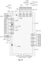
- Fig. 1 is a structural view of a display panel according to a first embodiment of the present application.
- the display panel provided by an embodiment of the present application includes a wireless communication structure.
- the wireless communication structure provided by an embodiment of the present application includes a loop structure 100 and antenna 200.
- the loop structure 100 includes a first connection end 110, a second connection end 120 and a coil body 130. At least a part of the coil body 130 is connected between the first connection end 110 and the second connection end 120.
- the antenna 200 includes a millimeter-wave antenna unit 210 configured to transmit and/or receive wireless signals in millimeter-wave band.
- the millimeter-wave antenna unit 210 is connected to the coil body 130 of at least one loop structure 100.
- the millimeter-wave antenna unit 210 configured to transmit and/or receive wireless signals in millimeter-wave band refers to the millimeter-wave antenna unit 210 configured to transmit and/or receive wireless signals in millimeter-wave band, that is, the "transmit and/or receive” herein refers to transmit and/or receive.
- the millimeter-wave antenna unit 210 includes a millimeter-wave feeding portion and a millimeter radiating portion.
- the millimeter-wave feeding portion and/or the millimeter radiating portion are connected to the coil body 130 of at least one loop structure 100.
- the wireless communication structure includes at least one loop structure 100 and the antenna 200.
- the loop structure 100 is configured to transmit and/or receive signals on the coil body 130 through the first connection end 110 and the second connection end 120.
- the antenna 200 includes the millimeter-wave antenna unit 210 configured to transmit and/or receive wireless signals in millimeter-wave band.
- the millimeter-wave antenna unit 210 is connected to the coil body 130 of at least one loop structure 100, which can not only reduce an overall area occupied by the loop structure 100 and the antenna 200, so that a plurality of wireless communication modules can be arranged in a limited space.
- At least one loop structure 100 and the millimeter-wave antenna unit 210 of the antenna 200 are connected to each other, which can ensure a desired optical performance of the display screen and simplify patterning process of the antenna, thereby improving the manufacturing efficiency and reducing the manufacturing cost of the wireless communication module.
- the display panel when the wireless communication structure is used for the display panel, the display panel further includes a touch-control layer 300 including a metal wiring in a grid pattern, which are illustrated as lightcolored grid lines in Fig. 1 .
- a touch-control layer 300 including a metal wiring in a grid pattern, which are illustrated as lightcolored grid lines in Fig. 1 .
- a connection part between at least one loop structure 100 and the millimeter-wave antenna unit 210 does not need to be cut in the connection direction, so that patterns of the metal wiring in a grid pattern in different areas tend to be uniform, and thus an optical effect of the display panel can be improved.
- the coil body 130 are is a loop coil, which may be arranged in various manners.
- the loop structure 100 includes at least one of a NFC coil, a wireless power charging (WPC) coil, a LTE coils, a GNSS coil, a WLAN coil, a BT coil, and a frequency modulation (FM) coil and the like.
- the NFC coil, the WPC coil, the LTE coil, the GNSS coil, the WLAN coil, the BT coil, the FM coil and the like can each be arranged as a loop coil, so as to facilitate the connection of the millimeter-wave antenna unit 210 therewith.
- the loop structure 100 includes at least one of the NFC coil and the WPC coil.
- the loop structure 100 including the NFC coil and/or the WPC coil is typically large in size.
- the loop structure 100 including the NFC coil and/or the WPC coil is arranged close to and around the edges of the display panel, so as to facilitate the series connection of the millimeter-wave antenna unit 210 in the loop structure 100 including the NFC coil and/or the WPC coil.
- the millimeter-wave antenna unit 210 can be arranged closer to the edges of the display panel, so that the deterioration of the optical and touch-control effects of the display panel caused by the millimeter-wave antenna unit 210 can be insignificant, and the feeding path of the millimeter-wave antenna unit 210 can be shorter. Therefore, feeding loss can be lower, so as to achieve a desired radiation performance of the millimeter-wave antenna unit 210.
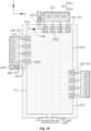
- Fig. 2 is schematic structural view of a display panel according to a second embodiment of the first aspect.
- the structure of the embodiment illustrated in Fig. 2 is partially the same as the structure of the embodiment illustrated in Fig. 1 , which will not be described in detail here, and differences therebetween will be described below.
- the following description herein will be directed to differences between various embodiments associated with respective drawings.
- the antenna 200 includes a plurality of millimeter-wave antenna units 210. At least two of the millimeter-wave antenna units 210 form a millimeter-wave antenna array 201. At least one millimeter-wave antenna unit 210 in the millimeter-wave antenna array 201 is connected to the coil body 130. In Fig. 2 , the position of the millimeter-wave antenna array 201 is indicated by a dashed-dotted line. The dashed-line frame does not limit the structure of the wireless communication structure of the embodiments of the present application.
- each millimeter-wave antenna unit 210 in the millimeter-wave antenna array 201 is connected to the coil body 130.
- the coil body 130 connected to the millimeter-wave antenna array 201 includes a first connection segment 131, a second connection segment 132 and a third connection segment 133.
- the first connection segment 131 is connected between the first connection end 110 and the millimeter-wave antenna array 201.
- the second connection segment 132 is connected between the millimeter-wave antenna array 201 and the second connection end 120.
- the third connection segment 133 is connected between two adjacent millimeter-wave antenna units 210 in a same millimeter-wave antenna array 201.
- the millimeter-wave antenna array 201 can be connected between the first connection end 110 and the second connection end 120.
- the third connection segment 133 is connected between two adjacent millimeter-wave antenna units 210 in a same millimeter-wave antenna array 201, which can reduce the overall area occupied by the loop structure 100 and the antenna 200, and can further simplify a pattern of the loop structure 100 and the antenna 200.
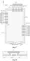
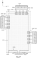
- Fig. 3 is a structural view of a display panel according to a third embodiment of the present application.
- the antenna 200 includes a plurality of millimeter-wave antenna arrays 201.
- the first connection segment 131 is connected between one of the millimeter-wave antenna arrays 201 and the first connection end 110.
- the second connection segment 132 includes a first sub-segment 132a and a second sub-segment 132b.
- the first sub-segment 132a is connected between two adjacent millimeter-wave antenna arrays 201
- the second sub-segment 132b is connected between another millimeter-wave antenna array 201 and the second connection end 120.
- the first sub-segment 132a is configured to realize the connection between the two adjacent millimeter-wave antenna arrays 201
- the second sub-segment 132b is configured to realize the connection between the millimeter-wave antenna array 201 and the second connection end 120.
- the second connection segment 132 is divided into a plurality of segments. Apart of the second connection segment 132 (for example, the first sub-segment 132a) is for connecting the two adjacent millimeter-wave antenna arrays 201, and a part of the second connection segment 132 (for example, the second sub-segment 132b) is for connecting the millimeter-wave antenna array 201 and the second connection end 120.
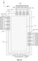
- the antenna 200 includes three millimeter-wave antenna arrays 201. Two of the millimeter-wave antenna arrays 201 are arranged as opposite to each other along a first direction X, that is, the two millimeter-wave antenna arrays 201 are correspondingly arranged on the two opposite edges of the display panel along the first direction X, and the two millimeter-wave antenna arrays 201 are not necessarily to be directly opposite to each other.
- the other millimeter-wave antenna array 201 is arranged as opposite to the first connection end 110 and the second connection end 120 along a second direction Y, so that the first connection end 110, the second connection end 120 and the three millimeter-wave antenna arrays 201 are distributed around the circumference of the display panel in a spaced manner, and the millimeter-wave antenna arrays 201 are distributed in different positions of the display panel.
- a user uses different gestures to operate the display panel, there is always a millimeter-wave antenna array 201 that is in a position that is not blocked by the user, so the stability of the millimeter-wave antenna array 201 for transmitting and/or receiving wireless signals can be improved, and a desired user wireless experience can be ensured.
- the first connection end 110 and the second connection end 120 may be arranged in a spaced manner from a millimeter-wave antenna array 201 along the first direction X, that is, the first connection end 110 and the second connection end 120 are arranged by the side of one of the millimeter-wave antenna arrays 201.
- the shape of the millimeter-wave antenna unit 210 may be set in various manners.
- the shape of the millimeter-wave antenna unit 210 may be a square, a diamond, or the like.
- the first connection segment 131, the second connection segment 132 and the third connection segment 133 can be arranged in various manners.
- the first connection segment 131 may include one wire, or the first connection segment 131 may include a plurality of wires arranged side by side, or the first connection segment 131 may include a plurality of wires arranged side by side and a bridge wire connecting the plurality of wires arranged side by side.
- the second connection segment 132 and/or the third connection segment 133 may comprise one wire, or the second connection segment 132 and/or the third connection segment 133 may include a plurality of wires arranged side by side, or the second connection segment 132 and/or the third connection segment 133 may include a plurality of wires arranged side by side and a bridge wire connecting the plurality of wires arranged side by side.
- the third connection segment 133 between two adjacent millimeter-wave antenna units 210 includes one wire.
- the third connection segment 133 between two adjacent millimeter-wave antenna units 210 includes two or more wires.
- An impedance of a conductor includes a resistance and a reactance.
- Resistance ⁇ (L/A), where ⁇ is a resistivity of the conductor, L is a length of the conductor, and A is a current distribution area corresponding to currents applied to the conductor.
- reactance inductive reactance - capacitive reactance
- reactance inductive reactance - capacitive reactance
- a frequency band of wireless signals in millimeter-wave band transmitted and/or received by the millimeter-wave antenna unit 210 is higher than the NFC frequency band. Therefore, under conditions of a same conductor, the millimeter-wave currents corresponding to the frequency band of the wireless signals in the millimeter-wave band are more likely to be blocked and less likely to be allowed to pass through compared to the currents corresponding to the NFC frequency band. Therefore, by adjusting the size of the coil body 130, the millimeter-wave currents can be desirably blocked and the currents corresponding to the NFC frequency band can be desirably allowed to pass through.
- the line width of at least part of at least one of the first connection segment 131, the second connection segment 132 and the third connection segment 133 is less than the width of the millimeter-wave antenna unit 210.
- the millimeter-wave antenna unit 210 includes a millimeter-wave wire.
- the line width of at least part of at least one of the first connection segment 131, the second connection segment 132 and the third connection segment 133 is not greater than the width of the millimeter-wave wire in the millimeter-wave antenna unit 210.
- the line width of at least part of the first connection segment 131 is not greater than the width of the millimeter-wave antenna unit.
- the millimeter-wave antenna unit 210 can be understood as including one millimeter-wave wire.
- the line width of at least part of the first connection segment 131 being less than the width of the millimeter-wave antenna unit 210 means that the line width of at least part of the first connection segment 131 is less than the sum of the widths of the plurality of millimeter-wave wires in the millimeter-wave antenna unit 210.
- the line width of at least part of the first connection segment 131 is not greater than the width of the millimeter-wave wire in the millimeter-wave antenna unit 210, the line width of the first connection segment 131 is small, so the first connection segment 131 has a high impedance.
- the wireless signals in millimeter-wave band transmitted and/or received by the millimeter-wave antenna unit 210 are in a high frequency band, so that the millimeter-wave currents corresponding to the frequency band of the wireless signals in millimeter-wave band transmitted and/or received by the millimeter-wave antenna unit 210 cannot pass through the first connection segment 131.
- the first connection segment 131 has a desired filtering and blocking effect on the millimeter-wave currents.
- the first connection segment 131 can have a desired passing effect on non-millimeter-wave current corresponding to the non-millimeter-wave frequency bands in the era of the 5th generation mobile communications (5G) and its previous generations mobile communications, WLAN or Bluetooth, and the first connection segment 131 can also have a desired passing effect on non-millimeter-wave current corresponding to the NFC frequency band. Therefore, in an embodiment of the present application, the current of the loop structure 100 can desirably pass through the first connection segment 131, while the millimeter-wave currents are significantly blocked by the first connection segment 131.
- the millimeter-wave currents refer to the currents corresponding to the frequency band of the wireless signals in millimeter-wave band transmitted and/or received by the millimeter-wave antenna unit 210.
- the wireless signal currents refer to the currents corresponding to the frequency band of the wireless signals transmitted and/or received by the loop structure 100.
- connection segment 132 and/or the third connection segment 133 being not greater than the width of the millimeter-wave antenna unit 210 and its beneficial effects are the same as above, and will not be repeated here.
- the line widths of the first connection segment 131, the second connection segment 132, and the third connection segment 133 are each set to be not greater than the line width of the millimeter-wave wire.
- the millimeter-wave currents can be significantly blocked by the first connection segment 131, the second connection segment 132, and the third connection segment 133, so as to desirably ensure the independence of each millimeter-wave antenna unit 210 in the millimeter-wave antenna array 201, and ensure a desired performance of the millimeter-wave antenna array 201.
- the line width of at least part of the third connection segment 133 is not greater than the width of the millimeter-wave antenna unit 210, as shown in Fig. 5 , when the third connection segment 133 between two adjacent millimeter-wave antenna units 210 includes one wire, the line width of one wire in the third connection segment 133 is not greater than the sum of the line widths of the millimeter-wave wires in the millimeter-wave antenna unit 210 in the same extension direction as the third connection segment 133. As shown in Fig.
- the third connection segment 133 between two adjacent millimeter-wave antenna units 210 includes a plurality of wires
- the sum of the line widths of the plurality of wires in the third connection segment 133 is not greater than the sum of the line widths of the millimeter-wave wires in the millimeter-wave antenna unit 210 in the same extension direction as the third connection segment 133.
- a line width direction of the third connection segment 133 is the first direction X
- the width direction of the millimeter-wave wire is also the first direction X.
- the third connection segment 133 extends along the first direction X
- the line width direction of the third connection segment 133 is the second direction Y
- the third connection segment 133 when the sum of the line widths of the wires in the third connection segment 133 is not greater than the sum of the line widths of the millimeter-wave wires in the millimeter-wave antenna unit 210 in the same extension direction as the third connection segment 133, that is, the width of the third connection segment 133 is small, the third connection segment 133 has a high impedance. Therefore, the third connection segment 133 has a desired filtering and blocking effect on the currents in the millimeter-wave band.
- the third connection segment 133 can have a desired passing effect on non-millimeter-wave current corresponding to the non-millimeter-wave frequency bands in the era of the 5th generation mobile communications (5G) and its previous generations mobile communications, WLAN, BT or GNSS, and the third connection segment 133 can also have a desired passing effect on non-millimeter-wave currents corresponding to the NFC frequency band. Therefore, in an embodiment of the present application, the current of the loop structure 100 can desirably pass through the third connection segment 133, while the millimeter-wave currents are significantly blocked by the third connection segment 133.
- the millimeter-wave currents can desirably flow in the millimeter-wave antenna unit 210, which can desirably ensure the independence of each millimeter-wave antenna unit 210 in the millimeter-wave antenna array 201 and ensure a desired performance of the millimeter-wave antenna array 201.
- the sum of the line widths of the wires in the second connection segment 132 is not greater than the sum of the line widths of the millimeter-wave wires in the millimeter-wave antenna unit 210 in the same extension direction as the second connection segment 132.
- the line width direction of the second connection segment 132 is the second direction Y
- the line width direction of the second connection segment 132 is the first direction X.
- the line width of the second connection segment 132 is small, which can desirably block the millimeter-wave currents, and desirably allow the currents corresponding to the non-millimeter-wave band and the NFC frequency band to pass through.
- the second connection segment 132 can desirably block the currents corresponding to the millimeter-wave band and ensure a desired performance of the millimeter-wave antenna array 201 and a desired performance of the millimeter-wave antenna unit 210, without much affecting the currents corresponding to other non-millimeter-wave band and the NFC frequency band.
- the sum of the line widths of the wires in the first connection segment 131 is not greater than the sum of the line widths of the millimeter-wave wires in the millimeter-wave antenna unit 210 in the same extension direction as the first connection segment 131.
- the line width direction of the first connection segment 131 is the second direction Y
- the line width direction of the first connection segment 131 is the first direction X.
- the line width of the first connection segment 131 is small, which can desirably block the millimeter-wave currents, and desirably allow the currents corresponding to the non-millimeter-wave band and the NFC frequency band to pass through.
- the first connection segment 131 can desirably block the currents corresponding to the millimeter-wave band and ensure a desired performance of the millimeter-wave antenna array 201 and a desired performance of the millimeter-wave antenna unit 210, without much affecting the currents corresponding to other non-millimeter-wave band and the NFC frequency band.
- the antenna 200 includes a plurality of millimeter-wave antenna units 210.
- the plurality of millimeter-wave antenna units 210 are arranged adjacently or in an array to form the millimeter-wave antenna array 201, which can improve the antenna gain and compensate for a large radiation path loss, and can achieve an effect of beam scanning to cover a wide space so as to reduce wireless communication blind spots and achieve a desired user wireless experience.
- the third connection segment 133 may be in the shape of a straight line, that is, the third connection segment 133 extends in a same direction.
- the third connection segment 133 may be in the shape of a polyline, that is, the third connection segment 133 extends along a bending path.
- the third connection segment 133 may be in the shape of an arc.
- the third connection segment 133 is formed by a combination of at least two of a straight line, a polyline, and an arc.
- the first connection segment 131 is connected to a first antenna unit among the plurality of millimeter-wave antenna units 210, or the second connection segment 132 is connected to a last antenna unit among the plurality of millimeter-wave antenna units 210.
- the millimeter-wave antenna array 201 includes four millimeter-wave antenna units 210.
- the four millimeter-wave antenna units 210 are respectively the first antenna unit, a second antenna unit, a third antenna unit and a fourth antenna unit along their arrangement direction (the second direction Y).
- the first antenna unit is positioned on a side, in the four millimeter-wave antenna units 210, close to the first connection end 110
- the fourth antenna unit is positioned on a side, in the four millimeter-wave antenna units 210, close to the second connection end 120.
- the first connection segment 131 is connected between the first antenna unit and the first connection end 110.
- the fourth antenna unit is the last antenna unit, and the second connection segment 132 is connected between the fourth antenna unit and the second connection end 120.
- the third connection segment 133 is connected between the first antenna unit and the second antenna unit, the third connection segment 133 is connected between the second antenna unit and the third antenna unit, and the third connection segment 133 is connected between the third antenna unit and the fourth antenna unit.
- the antenna 200 further includes a non-millimeter-wave antenna 202 for transmitting and/or receiving wireless signals in non-millimeter-wave band.
- the non-millimeter-wave antenna 202 is connected to the coil body 130.
- the millimeter-wave antenna unit 210 and the non-millimeter-wave antenna 202 are connected to the coil body 130, which can further improve a light-emitting effect of the display panel.
- the antenna 200 and the loop structure 100 are arranged in the touch-control layer 300, the number of cutting points can be further reduced and a touch effect can be improved.
- At least one millimeter-wave antenna unit 210 is reused as a part of the non-millimeter-wave antenna 202.
- the at least one millimeter-wave antenna unit 210 being reused as a part of the non-millimeter-wave antenna 202 may be implemented in a manner in which one millimeter-wave antenna unit 210 is reused as a part of the non-millimeter-wave antenna 202, or at least two adjacent millimeter-wave antenna units 210 are connected through the third connection segment 133 and reused as a part of the non-millimeter-wave antenna 202.
- At least two adjacent millimeter-wave antenna units 210 being connected through the third connection segment 133 and reused as a part of the non-millimeter-wave antenna 202 means that the at least two adjacent millimeter-wave antenna units 210, when connected through the third connection segment 133, can have the function of the non-millimeter-wave antenna 202 and be configured for transmitting and/or receiving wireless signals in non-millimeter-wave band.
- the non-millimeter-wave antenna 202 includes a first portion 2021 and a second portion 2022.
- the first portion 2021 is a radiating portion.
- the second portion 2022 is a feeding portion.
- One millimeter-wave antenna unit 210 may be reused as a part of the first portion 2021.
- one millimeter-wave antenna unit 210 and a part of the coil body 130 are connected to each other and reused as a part of the first portion 2021.
- two or more millimeter-wave antenna units 210 may be connected to one another and reused as the first portion 2021, and the first portion 2021 is connected to the second portion 2022.
- the at least one millimeter-wave antenna unit 210 may be connected to the feeding portion of the non-millimeter-wave antenna 202, that is, the at least one millimeter-wave antenna unit 210 may be connected to the second portion 2022 of the non-millimeter-wave antenna 202.
- the at least one millimeter-wave antenna unit 210 may be connected to the second portion 2022 of the non-millimeter-wave antenna 202 through a part of the coil body 130, so that the at least one millimeter-wave antenna unit 210 can be connected to a radio frequency integrated circuit of the non-millimeter-wave antenna 202, so as to realize the function of the non-millimeter-wave antenna 202.
- the at least two adjacent millimeter-wave antenna units 210 When at least two adjacent millimeter-wave antenna units 210 are connected through the third connection segment 133 and reused as at least a part of the non-millimeter-wave antenna 202, the at least two adjacent millimeter-wave antenna units 210 may be connected in series with one another or connected in parallel, and reused as at least a part of the non-millimeter-wave antenna 202.
- the reusing of the non-millimeter-wave antenna 202, the millimeter-wave antenna unit 210 and at least a part of the loop structure 100 can further simplify the area occupied by the various antennas and simplify the layout patterns of the various antennas. Therefore, the number of cutting spots in metal wiring in a grid pattern can be reduced, and a desired display performance and touch-control performance of the display panel can be ensured.
- the coil body 130 includes a blocking portion 140, and the blocking portion 140 is configured to allow wireless signal currents transmitted and/or received by the loop structure 100 to pass through and significantly block non-millimeter-wave currents transmitted and/or received by the non-millimeter-wave antenna 202 and millimeter-wave currents transmitted and/or received by the millimeter-wave antenna unit 210. Therefore, by providing the blocking portion 140, the non-millimeter-wave currents can be blocked, and the performance of the non-millimeter-wave antenna 202 can be designed and ensured in a better controllable manner.
- the blocking portion 140 is configured to allow wireless signal currents corresponding to the NFC frequency band to pass through.
- the blocking portion 140 is configured to allow wireless signal currents corresponding to the WPC frequency band to pass through.
- the blocking portion 140 can be arranged by changing the width of at least a part of the coil body 130, that is, the blocking portion 140 can be arranged by changing the thickness of the coil body 130, so as to block the currents corresponding to the non-millimeter-wave band.
- the user can set the positions, the widths, the lengths, the shapes, the film layer positions and the number of the blocking portions 140 according to the frequency band of the wireless signals in non-millimeter-wave band transmitted and/or received by the non-millimeter-wave antenna 202 and the frequency band of the wireless signals transmitted and/or received by the loop structure 100 in actual use, so as to block non-millimeter-wave currents and achieve the design of a target operating frequency in the non-millimeter-wave band.
- the width of the blocking portion 140 is set to be greater than the width of the other portion of the coil body 130.
- the width of the blocking portion 140 may not be greater than the width of the other portion of the coil body 130.
- the blocking portion 140 may be arranged on any one of the first connection segment 131, the second connection segment 132 and the third connection segment 133.
- the blocking portion 140 is arranged on the first sub-segment 132a shown in Fig. 7 , the millimeter-wave antenna units 210 of the millimeter-wave antenna array 201 between the first sub-segment 132a and the first connection end 110 are reused as the non-millimeter-wave antenna 202.
- the feeding portion (i.e., the second portion 2022) of the non-millimeter-wave antenna 202 is arranged between the first sub-segment 132a and the first connection end 110.
- the current of the non-millimeter-wave antenna 202 can flow toward the blocking portion 140, or the current of the non-millimeter-wave antenna 202 can flow toward the first connection end 110, thereby forming a dual-frequency band non-millimeter-wave antenna 202.
- the coil body 130 includes two or more blocking portions 140.
- the coil body 130 includes two blocking portions 140.
- One of the blocking portions 140 is positioned on the first sub-segment 132a, and the other blocking portion 140 is positioned on the first connection segment 131 between the second portion 2022 and the first connection end 110.
- the current of the non-millimeter-wave antenna 202 can flow toward the blocking portion 140 positioned on the first sub-segment 132a, or the current of the non-millimeter-wave antenna 202 can flow toward the blocking portion 140 positioned on the first connection segment 131, thereby forming a dual-frequency band non-millimeter-wave antenna 202.
- the frequency band of the non-millimeter-wave antenna 202 can be controlled, so as to achieve the purpose of more accurately controlling the frequency band of the wireless signals transmitted and/or received by the non-millimeter-wave antenna 202.
- the blocking portion 140 may be arranged on the third connection segment 133.
- two or more millimeter-wave antenna units 210 of the millimeter-wave antenna array 201 in Fig. 11 are reused as the non-millimeter-wave antenna 202, and the blocking portion 140 can be provided between the plurality of antenna units 210 reused as the non-millimeter-wave antenna array 201 and the other millimeter-wave antenna units 210.
- the blocking portions 140 are the first blocking portion 140a, the second blocking portion 140b and the third blocking portion 140c, respectively.
- the current flowing out from the second portion 2022 of the non-millimeter-wave antenna 202 can flow to the first blocking portion 140a, or the current flowing out from the second portion 2022 of the non-millimeter-wave antenna 202 can flow to the second blocking portion 140b.
- the non-millimeter-wave antenna 202 is a non-millimeter-wave antenna 202 covering a plurality of target frequency bands, that is, the currents flowing from the second portion 2022 to the first blocking portion 140a and the second blocking portion 140b are each a current in the frequency bands of the non-millimeter-wave antenna 202.
- the non-millimeter-wave antenna 202 in Fig. 11 is a non-millimeter-wave antenna 202 covering a single target frequency band.
- the current flowing out from the second portion 2022 of the non-millimeter-wave antenna 202 flows to the second blocking portion 140b, the current is a current in the target frequency band of the non-millimeter-wave antenna 202.
- An appropriate design of a wire path from the second portion 2022 to the first blocking portion 140a can have a beneficial effect on the performance of the target frequency band of the non-millimeter-wave antenna 202.
- a plurality of millimeter-wave antenna units 210 in the millimeter-wave antenna array 201 may be reused as two non-millimeter-wave antennas 202.
- the blocking portion 140 may be arranged between the plurality of millimeter-wave antenna units 210 reused as different non-millimeter-wave antenna arrays 201.
- the millimeter-wave antenna array 201 in Fig. 11 includes 4 millimeter-wave antenna units 210, wherein two adjacent millimeter-wave antenna units 210 are reused as the non-millimeter-wave antenna 202, then the blocking portion 140 can be arranged at a middle position of 4 millimeter-wave antenna units 210.
- the blocking portion 140 in the millimeter-wave antenna array 201 may be arranged between three millimeter-wave antenna units 210 and the other one millimeter-wave antenna unit 210.
- the blocking portion 140 may be arranged between two millimeter-wave antenna units 210 and the other three millimeter-wave antenna units 210, or the blocking portion 140 may be arranged between one millimeter-wave antenna unit 210 and the other four millimeter-wave antenna units 210.
- the blocking portion 140 can block the non-millimeter-wave currents
- the blocking portion 140 can block the millimeter-wave currents
- the line width of the blocking portion 140 may be less than that of the other portion of the coil body 130, or the line width of the blocking portion 140 may be greater than that of the other portion of the coil body 130.
- At least one millimeter-wave antenna unit 210 of one of the millimeter-wave antenna arrays 201 may be reused as a part of the non-millimeter-wave antenna 202.
- at least one millimeter-wave antenna unit 210 of each millimeter-wave antenna array 201 may be reused as a part of the non-millimeter-wave antenna 202 to increase the number of the non-millimeter-wave antennas 202.
- the display panel further includes a touch-control layer 300 including a metal wiring in a grid pattern, and the loop structure 100 and the antenna 200 are positioned in the touch-control layer 300.
- the loop structure 100 and the antenna 200 are arranged in the touch-control layer 300, so that the loop structure 100 and the antenna 200 can reuse the metal wiring in a grid pattern without adding a new structure layer, which can reduce the overall thickness of the display panel.
- the cutting points of the metal wiring in a grid pattern can be reduced, so as to ensure a desired touch-control effect of the touch-control layer 300 and the optical effect of the display panel at the same time.
- the millimeter-wave antenna unit 210 includes a plurality of first wires 211 extending along the first direction X and a plurality of second wires 211 extending along the second direction Y
- the first direction X is intersected with the second direction Y.
- the first direction X and the second direction Y are perpendicular to each other, or the angle between the first direction X and the second direction Y is 30 degrees, 45 degrees, 60 degrees, etc., as long as the first direction X is intersected with the second direction Y
- the millimeter-wave antenna unit 210 includes intersecting first wires 211 and second wires 212, that is, the millimeter-wave antenna unit 210 is in a grid pattern, which can increase an area of the millimeter-wave wires in the millimeter-wave antenna unit 210, thereby reducing the impedance of the millimeter-wave antenna unit 210, which can reduce the energy loss of the millimeter-wave antenna unit 210 and the energy reflection caused by impedance mismatch, so that the millimeter-wave antenna unit 210 can desirably transmit and/or receive wireless signals in the millimeter-wave band.
- the millimeter-wave antenna unit 210 can directly use the metal wires in the metal wiring in a grid pattern as the first wire 211 and the second wire 212, which can further simplify the formation of the millimeter-wave antenna unit 210.
- the millimeter-wave antenna unit 210 includes intersecting first wires 211 and second wires 212, that is, the millimeter-wave wires include intersecting first wires 211 and second wires 212.
- the touch-control layer 300 may be formed through intersection of a plurality of first touch-control lines parallel to the first wires 211 and a plurality of second touch-control lines parallel to the second wires 212.
- the display panel may further include an antenna layer.
- the loop structure 100 and the antenna 200 are positioned in the antenna layer.
- an antenna layer in a non-grid pattern is additionally provided in the display panel, so that the impedance of the antenna 200 and the loop structure 100 can be reduced, and the energy loss of the antenna 200 and the loop structure 100 and the energy reflection caused by impedance mismatch can be reduced, so as to improve the performance of the antenna 200 and the loop structure 100.
- the loop structure 100 and the antenna 200 in the antenna layer may be formed by etching.
- the antenna layer may be independently arranged and mounted on the display panel. Other embodiments may be selected to use for the formation the loop structure 100 and the antenna 200 in the antenna layer.
- the millimeter-wave antenna unit 210 may be in a block shape, so as to increase the area of the conductive material in the millimeter-wave antenna unit 210 and reduce the impedance of the millimeter-wave antenna unit 210 and the energy reflection caused by impedance mismatch, so that the millimeter-wave antenna unit 210 can have better performance for transmitting and/or receiving wireless signals of millimeter-waves.
- the millimeter-wave antenna unit 210 When the millimeter-wave antenna unit 210 is in a block shape, the millimeter-wave antenna unit 210 may be in a shape of a square, a diamond, a circle, or the like.
- the antenna layer may be arranged on a side of the touch-control layer 300 facing a cover plate of the display panel, or the antenna layer may be arranged on a side of the touch-control layer 300 facing away from the cover plate of the display panel.
- the millimeter-wave antenna unit 210 is connected to at least one of the plurality of coils.
- the plurality of coils may be connected in series, parallel or coupled with one another.
- the plurality of coils may be arranged to intersect or be spaced apart from one another.
- the millimeter-wave antenna unit 210 may be connected to one of the coils.
- the antenna 200 includes a plurality of millimeter-wave antenna units 210, different millimeter-wave antenna units 210 may be connected to different coils, or different millimeter-wave antenna units 210 may be connected to a same coil.
- the plurality of coils include an inner coil 101a and an outer coil 101b surrounding a side of the inner coil 101a away from the center of the wireless communication structure.
- Each of the inner coil 101a and the outer coil 101b is connected between the first connection end 110 and the second connection end 120. That is, the outer coil 101b is arranged closer to the edges of the wireless communication structure.
- the millimeter-wave antenna unit 210 may be connected to the inner coil 101a and/or the outer coil 101b.
- the millimeter-wave antenna unit 210 is connected to the outer coil 101b.
- the millimeter-wave antenna unit 210 being arranged closer to the edges of the display panel can reduce the influence of the millimeter-wave antenna unit 210 on the display effect of the display panel.
- the antenna 200 is arranged in the touch-control layer 300, since the user touches the edges of the display panel in a less frequency, the millimeter-wave antenna unit 210 being arranged close to the edges of the display panel can also reduce its influence on the touch-control effect.
- a part of the millimeter-wave antenna array 201 is connected with the inner coil 101a in series, and the other part of the millimeter-wave antenna array 201 is connected with the outer coil 101b in series.
- the antenna 200 further includes a millimeter-wave feeding portion 220 connected to the millimeter-wave antenna unit 210.
- the millimeter-wave antenna unit 210 is connected to the inner coil 101a.
- the millimeter-wave antenna unit 210 may be arranged in the same layer as the inner coil 101a and the outer coil 101b. At least a part of the millimeter-wave feeding portion 220 is arranged in a different layer from the outer coil 101b.
- the millimeter-wave feeding portion 220 and the outer coil 101b intersect, and at least a part of the millimeter-wave feeding portion 220 and the outer coil 101b being arranged in different layers can ensure that the millimeter-wave feeding portion 220 and the outer coil 101b are insulated from each other.
- the millimeter-wave feeding portion 220 includes a first conduction portion 221, a second conduction portion 222, and a bridge segment 223 connected between the first conduction portion 221 and the second conduction portion 222.
- the first conduction portion 221, the second conduction portion 222, and the outer coil 101b may be arranged in a same layer, and the bridge segment 223 and the outer coil 101b may be arranged in different layers, so as to ensure that the millimeter-wave feeding portion 220 and the outer coil 101b are insulated from each other.
- the entire millimeter-wave feeding portion 220 may be arranged in a different layer from the outer coil 101b.
- the touch-control layer 300 when the loop structure 100 and the antenna 200 are arranged in the touch-control layer 300, the touch-control layer 300 includes a first touch-control electrode and a second touch-control electrode arranged in a same layer.
- the connection portions between the adjacent first touch-control electrodes are arranged on the same layer as the first touch-control electrode, adjacent second touch-control electrodes need to be connected to one another through bridges, and the bridges and the second touch-control electrodes are arranged in different layers.
- the bridge segment 223 may be arranged in a same layer as the bridge of the touch-control layer 300, so as to further reduce the number of layers of the display panel and make the display panel lighter and thinner.
- the inner coil 101a and the outer coil 101b are spaced apart from each other and connected with each other in parallel.
- the inner coil 101a and the outer coil 101b are arranged independently from each other.
- Each of the inner coil 101a and the outer coil 101b is connected between the first connection end 110 and the second connection end 120.
- the coil bodies 130 are connected with one another in series and arranged in a spiral shape.
- the inner coil 101a and the outer coil 101b may be an inner coil part and an outer coil part of the spiral coil, that is, the inner coil 101a and the outer coil 101b are connected with each other in series.
- the inner coil 101a and the outer coil 101b are spiral coils, at least one of the first connection end 110 and the second connection end 120 overlaps with a part of the coil, and at least one of the first connection end 110 and the second connection end 120 may be arranged in different layers from a part of the coil body 130.
- an embodiment of the present application takes that the first connection end 110 and a part of the coil body 130 overlap and are arranged in different layers as an example for illustration.
- the first connection end 110 may be set to overlap with the coil body 130 which is arranged in the plurality of turns.
- the first connection end 110 is set to overlap with the coil body 130.
- the first connection end 110 includes a first segment 111, a second segment 112, and a spanning segment 113 connecting the first segment 111 and the second segment 112.
- the first segment 111 and the second segment 112 are positioned on two sides of the coil body 130, respectively.
- the spanning segment 113 and the coil body 130 are arranged in different layers, and an insulation layer is arranged between the spanning segment 113 and the coil body 130.
- the spanning segment 113 may be arranged in the same layer as the bridge connecting the touch-control electrodes.
- the plurality of coils include a first coil 101e and a second coil 101f.
- Each of the first coil 101e and the second coil 101f is connected between the first connection end 110 and the second connection end 120.
- a part of the first coil 101e is positioned on a side of the second coil 101f away from the center of the wireless communication structure, and a part of the second coil 101f is positioned on a side of the first coil 101e away from the center of the wireless communication structure.
- the millimeter-wave antenna unit 210 may be connected to the first coil 101e and/or the second coil 101f.
- a top portion of the first coil 101e is positioned inside a top portion of the second coil 101f, and a side portion of the first coil 101e is positioned outside a side portion of the second coil 101f In this way, the lengths of the first coil 101e and the second coil 101f can be made similar or the same, so that the current in a same frequency band can flow on the first coil 101e and the second coil 101f.
- the plurality of coils include a coupled coil 101c and a direct-fed coil 101d.
- the direct-fed coil 101d is connected between the first connection end 110 and the second connection end 120.
- the coupled coil 101c is arranged by the side of the direct-fed coil 101d and spaced apart from the direct-fed coil 101d.
- the coupled coil 101c being connected to the direct-fed coil 101d by coupling means that the coupled coil 101c does not have a direct connection relationship with other coils (including the direct-fed coil 101d) and the coupled coil 101c is for coupling with the direct-fed coil 101d to generate signals.
- the millimeter-wave antenna unit 210 may be connected to the coupled coil 101c and/or the direct-fed coil 101d.
- the coupled coil 101c is positioned on a side of the direct-fed coil 101d away from the center of the wireless communication structure, and the millimeter-wave antenna unit 210 is connected to the coupled coil 101c.
- the coupled coil 101c is positioned on a side of the direct-fed coil 101d close to the edges of the display panel, and the millimeter-wave antenna unit 210 is connected to the coupled coil 101c, so that the millimeter-wave antenna unit 210 is arranged closer to the edges of the display panel.
- the millimeter-wave antenna unit 210 is arranged in the touch-control layer 300, the influence of the millimeter-wave antenna unit 210 on the touch-control effect of the touch-control layer 300 can be reduced.
- the millimeter-wave antenna unit 210 is arranged close to the edges of the display panel instead of close to the center of the display panel, which can also reduce the influence of the millimeter-wave antenna unit 210 on the display effect of the display panel.
- the direct-fed coil 101d is positioned on the side of the coupled coil 101c away from the center of the wireless communication structure, and the millimeter-wave antenna unit 210 is connected to the direct-fed coil 101d.
- the millimeter-wave antenna unit 210 is arranged closer to the edge of the display panel.
- the performance of the loop structure 100 in transmitting and/or receiving wireless signals can be improved.
- the coupled coil 101c can improve the performance of the NFC coil in transmitting and/or receiving wireless signals in the NFC frequency band.
- the display panel includes a first area M and a second area N surrounding the first area M.
- the loop structure 100 is positioned in the second area N.
- the second area N surrounds the first area M, so that the second area N is arranged closer to the edges of the display panel.
- the loop structure 100 is positioned in the second area N, which can improve the influence of the loop structure 100 and the antenna 200 on the display effect of the display panel.
- the antenna 200 may be positioned in the second area N, or the antenna 200 may also be partially arranged in the first area M.
- the second area N may be arranged in various manners.
- the second area N may include a display area; and/or the second area N may include a non-display area.
- the loop structure 100 is positioned in the non-display area, which can desirably reduce the influence of the loop structure 100 on the display effect and the touch-control effect.
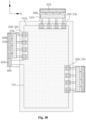
- the loop structure 100 may be arranged in the first area M in various manners. For example, as shown in Fig. 24 , the loop structure 100 is arranged around the first area M in the second area N, which can increase an extension length of the loop structure 100 and the extension length of the coil body 130 of the loop structure 100, so as to implement a designed target frequency band and enhance the wireless performance of the frequency band.
- the first connection end 110 and the second connection end 120 are arranged close to each other.
- the coil body 130 extends around the first area M from the first connection end 110 and then is connected to the second connection end 120.
- the distance between the first connection end 110 and the second connection end 120 is small, which not only facilitates the integration of a connector for transmitting signals from/to the first connection end 110 and a connector for transmitting signals from/to the second connection end 120, but also increases the extension length of the coil body 130 to implement the designed target frequency band, thereby enhancing the wireless performance of the frequency band.
- the coil body 130 is formed as extending along a winding path.
- a same coil body 130 includes a first extension segment 130a and a second extension segment 130b that overlap with each other in a direction approaching the edges of the wireless communication structure.
- the coil body 130 extends along the winding path, and one part of the coil body 130 overlaps another part of the coil body 130 in the direction approaching the edges of the wireless communication structure, which can increase the extension length of the coil body 130 to implement the designed target frequency band, and improve the wireless performance of the coil body 130.
- the millimeter wave antenna unit 210 is connected to the second extension segment 130b.
- the second extension segment 130b is closer to the edges of the display panel compared to the first extension segment 130a.
- the millimeter-wave antenna array 201 is connected to the second extension segment 130b in series, the millimeter-wave antenna array 201 is closer to the edge of the display panel, which can reduce the influence of the millimeter-wave antenna array 201 on the touch-control effect and the display effect of the display panel.
- the first extension segment 130a and the second extension segment 130b may be arranged on the inner coil 101a, which can also increase the extension length of the coil body 130, so as to implement the designed target frequency band and improve the wireless performance of the coil body 130.
- At least a part of the coil body 130 is formed as extending along a winding path.
- at least a part of the coil body 130 is formed as extending along a winding serpentine path, so that the extension length of the coil body 130 can be increased, so as to implement the designed target frequency band and improve the wireless performance of the coil body 130.
- At least a part of the coil body 130 includes a first section 130c and a second section 130d connected to each other, that is, at least a part of the coil body 130 is provided with a double-stranded wire, which can reduce the impedance of the coil body 130 and thus energy loss and energy reflection caused by impedance mismatch, thereby improving the wireless performance of the coil body 130.
- the millimeter-wave antenna unit 210 is not aligned with the first section 130c or the second section 130d, that is, the millimeter-wave antenna array 201 is connected to the non-double-stranded wire portion of the coil body 130, which can simplify the connection between the millimeter-wave antenna array 201 and the coil body 130.
- the millimeter-wave antenna unit 210 may be a single-polarization millimeter-wave antenna unit.
- the millimeter-wave antenna unit 210 is a dual-polarization millimeter-wave antenna unit.
- different parts of the coil body 130 may be arranged in a same layer, that is, the first connection segment 131, the second connection segment 132 and the third connection segment 133 may be arranged in a same layer.
- different parts of the coil body 130 may be arranged in different layers.
- at least two of the first connection segment 131, the second connection segment 132 and the third connection segment 133 are positioned in different film layers. Different parts of at least one of the first connection segment 131, the second connection segment 132 and the third connection segment 133 may be positioned in a same layer.
- different parts of at least one of the first connection segment 131, the second connection segment 132 and the third connection segment 133 may be positioned in different layers.
- different parts of the first connection segment 131 may be positioned in different layers
- different parts of the second connection segment 132 may be positioned in different layers
- different parts of the third connection segment 133 may be positioned in different layers.
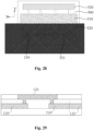
- Fig. 29 is a partial cross-sectional view taken along line A-A in Fig. 5 in a twenty seventh embodiment.
- the second connection segment 132 and the millimeter-wave antenna unit 210 may be arranged in a same layer, and the third connection segment 133 and the second connection segment 132 may be arranged in different layers.
- an embodiment of the present application further provides a wireless communication apparatus, including the display panel according to any foregoing embodiment of the first aspect. Since the wireless communication apparatus provided by an embodiment of the present application includes the display panel of any of the above embodiments, the wireless communication apparatus provided by an embodiment of the present application has the beneficial effects of the display panel of any of the above embodiments of the first aspect, and will not be repeated here.
- the wireless communication apparatus in an embodiment of the present application include but are not limited to a device with display functions, such as a cell phone, a wireless wearable device, a personal digital assistant (PDA for short), a tablet computer, an e-book, a television, an access control, a smart fixed phone, a console, or the like.
- a device with display functions such as a cell phone, a wireless wearable device, a personal digital assistant (PDA for short), a tablet computer, an e-book, a television, an access control, a smart fixed phone, a console, or the like.
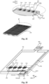
- the wireless communication apparatus further includes a first circuit board 400, a second circuit board 500, a first transmission line disposed on the first circuit board 400 and a second transmission line disposed on the second circuit board 500.
- the first transmission line is in communication with the first connection end 110 and/or the second connection end 120 of at least one coil body 130.
- the second transmission line is in communication with the millimeter-wave antenna unit 210.
- the antenna 200 includes at least two millimeter-wave antenna units 210. Two or more millimeter-wave antenna units 210 form a millimeter-wave antenna array 201.
- the antenna 200 includes a plurality of millimeter-wave antenna arrays 201.
- the wireless communication apparatus includes a plurality of circuit boards corresponding to the plurality of millimeter-wave antenna arrays 201 respectively.
- the circuit boards corresponding to the plurality of millimeter-wave antenna arrays 201 may be the second circuit boards 500, so that the millimeter-wave antenna array 201 can transmit signals with the corresponding second circuit board 500 nearby.
- the first circuit board 400 and the second circuit board 500 may be arranged in various manners.
- the first circuit board 400 and the second circuit board 500 may be provided separately from each other.
- the first circuit board 400 is integrated with the second circuit board 500, which can simplify the structure of the wireless communication apparatus.
- the wireless communication apparatus may further include a first integrated circuit in communication with the first connection end 110 and/or the second connection end 120 through the first transmission line.
- the first integrated circuit may be arranged in various positions.
- the first integrated circuit may be arranged on the first circuit board 400, or the first integrated circuit may be directly arranged on a printed circuit board (PCB) of the wireless communication apparatus.
- PCB printed circuit board
- the wireless communication apparatus may further include a second integrated circuit 510 in communication with the millimeter-wave antenna unit 210 through the second transmission line.
- the second integrated circuit 510 may be arranged in various positions.
- the second integrated circuit 510 may be arranged on the second circuit board 500, or the second integrated circuit 510 may be directly arranged on the PCB of the wireless communication apparatus.
- the first integrated circuit being arranged on the PCB of the wireless communication apparatus and the second integrated circuit 510 being arranged on the second circuit board 500 is taken as an example for illustration.
- the first integrated circuit is an NFC radio frequency integrated circuit.
- the second integrated circuit 510 is in communication with the millimeter-wave antenna unit 210, the second integrated circuit 510 is a millimeter-wave radio frequency integrated circuit. Due to the filtering and frequency selectivity of the millimeter-wave radio frequency circuit, the current in the NFC frequency band and the current in other non-millimeter-wave bands are significantly blocked by the millimeter-wave radio frequency circuit, and signals in the NFC frequency band and signals in other non-millimeter-wave band do not have significant influence on the performance of the millimeter-wave radio frequency circuit, so as that a desired performance of the millimeter-wave radio frequency circuit can be ensured.
- the wireless communication apparatus when the antenna includes a plurality of millimeter-wave antenna arrays 201, the wireless communication apparatus includes a plurality of second circuit boards 500 and a plurality of second integrated circuits 510.
- the second integrated circuits 510 are in communication with the millimeter-wave antenna arrays 201 through the second transmission lines on the second circuit boards 500.
- a plurality of second circuit boards 500 may be provided separately from each other, and a first circuit board 400 may be integrated with any of second circuit boards 500.
- a plurality of second circuit boards 500 may be formed integrally, that is, a first circuit board 400 may be integrated with a plurality of second circuit boards 500, which can further simplify the structure of the wireless communication apparatus.
- the wireless communication apparatus further includes a first connection socket 420 and a second connection socket 520.
- the first connection socket 420 is provided on the first circuit board 400 and is in communication with the first transmission line on the first circuit board 400, which enables the communication between the first integrated circuit and the coil body 130 through the first connection socket 420.
- the second connection socket 520 is provided on the second circuit board 500 and is in communication with the second integrated circuit 510 on the second circuit board 500, which enables the signal transmission between the second integrated circuit 510 and the PCB of the wireless communication apparatus.
- the first connection socket 420 is configured to enable the communication between the coil body 130 and the first integrated circuit
- the second connection socket 520 is configured to enable the communication between the second integrated circuit 510 and the PCB of the wireless communication apparatus.
- the first connection socket 420 and the second connection socket 520 may be arranged in various manners. For example, when the first circuit board 400 and the second circuit board 500 are provided separately from each other, the first connection socket 420 and the second connection socket 520 are provided separately from each other.
- the first connection socket 420 is integrated with the second connection socket 520, which can further simplify the structure of the wireless communication apparatus.
- the antenna 200 further includes the non-millimeter-wave antenna 202.
- the non-millimeter-wave antenna 202 at least one millimeter-wave antenna unit 210 is reused as a part of the non-millimeter-wave antenna 202.
- the wireless communication apparatus may further include a third circuit board 600 and a third transmission line disposed on the third circuit board 600, the third transmission line is in communication with the non-millimeter-wave antenna 202.
- At least two of the third circuit board 600, the second circuit board 500 and the first circuit board 400 are formed integrally to simplify the structure of the wireless communication apparatus.
- there are a plurality of millimeter-wave antenna arrays 201 there are a plurality of second circuit boards 500, and at least one of the third circuit board 600 and the first circuit board 400 may be integrated with at least one of the second circuit boards 500.
- the wireless communication apparatus further includes a third connection socket 620 disposed on the third circuit board 600 and being in communication with the third transmission line.
- the wireless communication apparatus further includes a third integrated circuit 610 disposed on the third circuit board 600.
- the third connection socket 620 is in communication with the third integrated circuit 610 and is configured to enable the communication between the third integrated circuit 610 and the PCB of the wireless communication apparatus.
- the third integrated circuit 610 is in communication with the non-millimeter-wave antenna 202, so the third integrated circuit 610 is a non-millimeter-wave radio frequency integrated circuit. Because the non-millimeter-wave radio frequency integrated circuit and the NFC radio frequency integrated circuit have the filtering and frequency selectivity, signals in other non-millimeter-wave bands do not have a significant influence on the NFC radio frequency integrated circuit, or NFC signals do not have a significant influence on the radio frequency integrated circuits corresponding to other non-millimeter-wave bands, so as to ensure a desired performance of the NFC radio frequency integrated circuit or radio frequency integrated circuits corresponding to other non-millimeter-wave bands.
- the third integrated circuit 610 is a non-millimeter-wave radio frequency integrated circuit
- the second integrated circuit 510 is a millimeter-wave radio frequency integrated circuit
- the first integrated circuit 410 is a non-NFC radio frequency integrated circuit. Due to the filtering and frequency selectivity of the NFC radio frequency circuit, signals in the millimeter-wave band and the non-millimeter-wave band do not have a significant influence on the performance of the NFC radio frequency integrated circuit.
- connection sockets including the first connection socket 420, the second connection socket 520 and the third connection socket 620
- at least two of the first connection socket 420, the second connection socket 520 and the third connection socket 620 are formed integrally to simplify the structure of the wireless communication apparatus.
- there are a plurality of millimeter-wave antenna arrays 201 there are a plurality of second connection sockets 520, and the third connection socket 620 and the first connection socket 420 may be integrated with at least one of the second connection sockets 520.
- the first circuit board 400, one of the second circuit boards 500 and the third circuit board 600 are formed integrally, and the first connection socket 420, one of the second connection sockets 520 and the third connection socket 620 are formed integrally to simplify the structure of the wireless communication apparatus as much as possible.
- the wireless communication apparatus includes a display panel.
- the display panel includes a loop structure 100 and an antenna 200.
- the antenna 200 includes a millimeter-wave antenna unit 210 and a non-millimeter-wave antenna 202.
- the millimeter-wave antenna unit 210 and the non-millimeter-wave antenna 202 are connected to the loop structure 100.
- the millimeter-wave antenna unit 210 and the millimeter-wave feeding portion 220 are connected with each other.
- a plurality of millimeter-wave antenna units 210 form a millimeter-wave antenna array 201.
- the non-millimeter-wave antenna 202 includes a first portion 2021 and a second portion 2022. At least a part of the first portion 2021 is formed by reusing at least one millimeter-wave antenna unit 210.
- the second portion 2022 is a feeding portion of the non-millimeter-wave antenna array 202.
- the wireless communication apparatus further includes the first circuit board 400, the second circuit board 500 and the third circuit board 600.
- the wireless communication apparatus includes the first connection socket 420 disposed on the first circuit board 400, the first connection socket 420 is configured to communicate with the loop structure 100.
- the wireless communication apparatus includes the second integrated circuit 510 and the second connection socket 520 disposed on the second circuit board 500.
- the wireless communication apparatus includes the third integrated circuit 610 and the third connection socket 620 disposed on the third circuit board 600.
- the second circuit board 500 and the third circuit board 600 being integrally formed and the second connection socket 520 and the third connection socket 620 being integrally formed is taken as an example for illustration.
- first circuit board 400, the second circuit board 500 and the third circuit board 600 may be integrally formed, and the first connection socket 420, the second connection socket 520 and the third connection socket 620 may also be integrally formed.
- the wireless communication apparatus further includes a substrate 700.
- the loop structure 100 and the antenna 200 are arranged in the touch-control layer 300.
- the touch-control layer 300 is arranged on the substrate 700.
- the second circuit board 500 and the third circuit board 600 may be arranged in the non-display area of the wireless communication apparatus.
- the second circuit board 500 and the third circuit board 600 are flexible circuit boards.
- the second integrated circuit 510 and the third integrated circuit 610 may be respectively bound to the second circuit board 500 and the third circuit board 600 by a chip on film (COF) process.
- COF chip on film
- the first circuit board 400 may also be a flexible circuit board and is bent to the non-display side of the wireless communication apparatus.
- the second integrated circuit 510 and the third integrated circuit 610 may be bound to a same circuit board by the COF process.
- the loop structure 100, the millimeter-wave antenna array 201 and the non-millimeter-wave antenna 202 are all used for wireless communication having a corresponding frequency band.
- the loop structure 100 may include a coupled portion and a feeding portion, while the non-millimeter-wave antenna 202 includes a radiating portion and a feeding portion.
- the coil body 130 is a coupled portion of the loop structure 100.
- the first connection end 110 and the second connection end 120 are the feeding portion of the loop structure 100.
- the loop structure 100 may be short-distance fixedpoint wireless communication.
- transmission frequencies of the millimeter wave antenna array 201 are different form the transmission frequencies of non-millimeter wave antenna 202.
- frequencies of non-millimeter waves commonly used in the mobile wireless communication are higher than 24.25 GHz, that is to say, the millimeter wave antenna array 201 refers to an antenna array that transmits/receives wireless signals having frequencies higher than 24.25 GHz.
- frequencies of non-millimeter waves commonly used in mobile wireless communication are higher than 410 MHz and lower than 7.125 GHz
- the non-millimeter wave antenna 202 refers to an antenna that transmits/receives wireless signals having frequencies higher than 410 MHz and lower than 7.125 GHz.
- the coil body 130 transmits/receives wireless signals through coupling, and frequencies of the wireless signals transmitted/received by the coil body 130 through coupling may be lower than 410 MHz.
- the millimeter wave antenna array 201 and the non-millimeter wave antenna 202 are antennas configured for mobile wireless communication. That is to say, the millimeter wave antenna array 201 and the non-millimeter wave antenna 202 are antennas used for mobile wireless communication.
- the communication frequency band of the non-millimeter-wave antenna in mobile wireless communication is 410 MHz to 7.125 GHz.
- the non-millimeter-wave antenna 202 herein usually refers to antenna corresponding to the non-millimeter-wave band in mobile wireless communication (including cellular antennas in 5G and previous generation, WLAN antennas, Bluetooth antennas, GNSS antennas, etc.).
- the loop structure 100 is the NFC coil, and a communication frequency band of the NFC coil is, for example, 13.56 MHz.
- the loop structure 100 is the WPC coil, and a communication frequency band of a commonly used WPC coil is, for example, higher than or equal to 100 kHz.
- the NFC coil and the WPC coil are coupled coils used in non-mobile wireless communication (because currently the NFC coil and the WPC coil need to be geologically referenced to a counterpart communication apparatus).
- the loop structure 100 may further include the frequency modulation (FM) coil.
- FM frequency modulation
- a frequency band of the common FM is 87 MHz-108 MHz, and the FM coil is applied to long-distance wireless non-mobile communication.
Landscapes
- Engineering & Computer Science (AREA)
- Theoretical Computer Science (AREA)
- General Engineering & Computer Science (AREA)
- Computer Networks & Wireless Communication (AREA)
- Physics & Mathematics (AREA)
- Human Computer Interaction (AREA)
- General Physics & Mathematics (AREA)
- Electromagnetism (AREA)
- Support Of Aerials (AREA)
- Variable-Direction Aerials And Aerial Arrays (AREA)
- Near-Field Transmission Systems (AREA)
- Details Of Aerials (AREA)
- Developing Agents For Electrophotography (AREA)
- Transceivers (AREA)
Abstract
Description
- This application claims priority to
Chinese Patent Application No. 202210433198.7, filed on April 24, 2022 - The present application relates to the technical field of display devices, and particularly to a wireless communication structure, a display panel and a wireless communication apparatus.
- Handheld wireless communication apparatuses (e.g. cell phones, smart watches, etc.) have more and more functions, and market requirements on apparatus appearance and wireless communication performance are becoming higher and higher. In the era of the 5th generation mobile communications (5G), since both the millimeter-wave (mm-wave) band and the non-millimeter wave (non-mm-wave) band are involved, types and numbers of modules used for wireless communication in a handheld wireless communication apparatuses are increasing. In addition, functions of near field communication (NFC) are becoming increasingly popular, so NFC coils have been provided in more and more handheld wireless communication apparatuses.
- Meanwhile, screen-to-body ratios of the handheld wireless communication apparatus are becoming higher and higher. Therefore, since overall sizes of the apparatuses cannot be significantly increased, arranging wireless communication modules in display panels is a critical technology trend in foreseeable future. However, internal spaces of the display panels are limited and the display panels have optical requirements, so how to arrange the wireless communication modules in the display panels has become an important technical problem to be solved urgently.
- Embodiments of the present application provide a wireless communication structure, a display panel, and a wireless communication apparatus, in order to solve the problem of how to arrange a wireless communication module in a limited space and ensure a desired optical performance of the display panel.
- Embodiments of a first aspect of the present application provides a wireless communication structure, including: a loop structure including a first feeding end, a second feeding end and a coil body, at least a part of the coil body being connected between the first feeding end and the second feeding end; an antenna including a plurality of millimeter-wave antenna units configured to transmit and/or receive wireless signals in millimeter-wave band, wherein at least two of the plurality of millimeter-wave antenna units form a millimeter-wave antenna array; the at least two millimeter-wave antenna units in the millimeter-wave antenna array are connected to the coil body, the coil body includes a first connection segment, a second connection segment and a third connection segment, the first connection segment is connected between the first connection end and the millimeter-wave antenna array, the second connection segment is connected between the millimeter-wave antenna array and the second connection end, and the third connection segment is connected between two adjacent millimeter-wave antenna units in the millimeter-wave antenna array.
- Embodiments of a second aspect of the present application provide a display panel including the wireless communication structure according to any one of the above embodiments of the first aspect.
- Embodiments of a third aspect of the present application provide a wireless communication apparatus including the display panel according to any one of the above embodiments of the first aspect.
- In the wireless communication structure provided by the present application, the wireless communication structure includes the loop structure and the antenna. The loop structure includes the first connection end, the second connection end and the coil body, and the loop structure is configured to transmit and/or receive wireless signals on the coil body through the first connection end and the second connection end. The antenna includes the millimeter-wave antenna unit. The millimeter-wave antenna unit is configured to transmit and/or receive wireless signals in millimeter-wave band. The millimeter-wave antenna unit is connected to the coil body, so that at least a part of the coil body can transmit and/or receive wireless signals of the loop structure and wireless signals in millimeter-wave band. The overall area occupied by the loop structure and the antenna can be reduced, so that a plurality of modules used for wireless communication can be arranged in a limited space. In addition, at least one loop structure is connected to the millimeter-wave antenna unit, which can ensure a desired optical performance of the display screen, and simply the patterning process of the antenna, thereby improving the manufacturing efficiency of the wireless communication module and reducing the manufacturing cost.
- Features, objects and advantages of the present application will be clearer from the detailed description of following reference drawings of non-limited embodiments. The same or similar reference numerals and/or letters mean the same or similar features.
-
Fig. 1 is a schematic structural view of a display panel according to a first embodiment of a first aspect of the present application. -
Fig. 2 is a schematic structural view of a display panel according to a second embodiment of a first aspect of the present application. -
Fig. 3 is a schematic structural view of a display panel according to a third embodiment of a first aspect of the present application. -
Fig. 4 is a schematic structural view of a display panel according to a fourth embodiment of a first aspect of the present application. -
Fig. 5 is a partial magnified structural view ofFig. 4 . -
Fig. 6 is a partial magnified structural view of a millimeter-wave antenna unit in a fifth embodiment. -
Fig. 7 is a schematic structural view of a display panel according to a sixth embodiment of a first aspect of the present application. -
Fig. 8 is a schematic structural view of a display panel according to a seventh embodiment of a first aspect of the present application. -
Fig. 9 is a partial magnified structural view ofFig. 8 . -
Fig. 10 is a schematic structural view of a display panel according to an eighth embodiment of a first aspect of the present application. -
Fig. 11 is a schematic structural view of a display panel according to a ninth embodiment of a first aspect of the present application. -
Fig. 12 is a schematic structural view of a display panel according to a tenth embodiment of a first aspect of the present application. -
Fig. 13 is a schematic structural view of a display panel according to an eleventh embodiment of a first aspect of the present application. -
Fig. 14 is a schematic structural view of a display panel according to a twelfth embodiment of a first aspect of the present application. -
Fig. 15 is a schematic structural view of a display panel according to a thirteenth embodiment of a first aspect of the present application. -
Fig. 16 is a schematic structural view of a display panel according to a fourteenth embodiment of a first aspect of the present application. -
Fig. 17 is a schematic structural view of a display panel according to a fifteenth embodiment of a first aspect of the present application. -
Fig. 18 is a partial cross-sectional view ofFig. 17 . -
Fig. 19 is a schematic structural view of a display panel according to a sixteenth embodiment of a first aspect of the present application. -
Fig. 20 is a partial cross-sectional view ofFig. 19 . -
Fig. 21 is a schematic structural view of a display panel according to a seventeenth embodiment of a first aspect of the present application. -
Fig. 22 is a schematic structural view of a display panel according to an eighteenth embodiment of a first aspect of the present application. -
Fig. 23 is a schematic structural view of a display panel according to a nineteenth embodiment of a first aspect of the present application. -
Fig. 24 is a schematic structural view of a display panel according to a twentieth embodiment of a first aspect of the present application. -
Fig. 25 is a schematic structural view of a display panel according to a twenty first embodiment of a first aspect of the present application. -
Fig. 26 is a schematic structural view of a display panel according to a twenty second embodiment of a first aspect of the present application. -
Fig. 27 is a schematic structural view of a display panel according to a twenty third embodiment of a first aspect of the present application. -
Fig. 28 is a schematic structural view of a display panel according to a twenty fourth embodiment of a first aspect of the present application. -
Fig. 29 is a partial cross-sectional view ofFig. 5 . -
Fig. 30 is a schematic structural view of a wireless communication apparatus according to a first embodiment of a second aspect of the present application. -
Fig. 31 is a schematic structural view of a wireless communication apparatus according to a second embodiment of a second aspect of the present application. -
Fig. 32 is a schematic structural view of a wireless communication apparatus according to a third embodiment of a second aspect of the present application. -
Fig. 33 is a schematic structural view of a wireless communication apparatus according to a fourth embodiment of a second aspect of the present application. -
Fig. 34 is a schematic structural view of a wireless communication apparatus according to a fifth embodiment of a second aspect of the present application. -
Fig. 35 is a schematic structural view of a wireless communication apparatus according to a sixth embodiment of a second aspect of the present application. -
Fig. 36 is a schematic structural view of a wireless communication apparatus according to a seventh embodiment of a second aspect of the present application. -
Fig. 37 is a schematic structural view of a wireless communication apparatus in the related art. - Features and exemplary embodiments of various aspects of the present application are described in detail below. In the following detailed description, numerous specific details are presented to provide a thorough understanding of the present application. However, it will be apparent for those skilled in the art that the present application may be implemented without some of these specific details. The following description of the embodiments is merely for providing a better understanding of the present application by illustrating examples of the present application. In the drawings and the following description, at least some of well know structures and techniques have not been shown to avoid unnecessary obscurity of the present application. In addition, size of some structures may be exaggerates for clarity. Furthermore, the features, structures, or characteristics described below may be combined in one or more embodiments by any suitable manner.
- With the development of display technology and wireless communication technology, screen-to-body ratios of display devices in apparatuses with wireless communication functions are continually increasing, and types and numbers of modules used to achieve wireless communication in the apparatuses are also increasing. For example, in the era of 5th generation mobile communications, spectrum of wireless communication cover both the millimeter wave band and the non-millimeter wave band. Therefore, a wireless communication apparatus with 5G millimeter wave functions, such as a mobile phone, not only may be provided with a first type antenna that can be used for the millimeter wave band, but also may be provided with a wireless communication module that can be used for the non-millimeter wave band (such as those used for 5G, 4G, a wireless local area network (WLAN), Bluetooth (BT), a global navigation satellite system (GNSS), etc). At the same time, near field communication (NFC) is also becoming increasingly popular, and therefore, more and more mobile phones have NFC coils provided therein.
- However, the higher the screen-to-body ratio of the display device in the wireless communication apparatus is, the more likely it is to limit the positions where the wireless communication modules can be positioned, and the wireless communication modules tend to be more likely to be obscured in use (for example, the apparatus is being held by hand or placed on a metal table), which results in that the performance of wireless communication module deteriorates significantly, and which affects the users' wireless experience. In view of the above, it is contemplated that the wireless communication modules are integrated in the display device of the wireless communication apparatus, for example, in a design of Antenna-on-Display (AoD), which has become a possible direction of development for wireless communication modules in wireless communication apparatuses.
- In some embodiments, with reference to
Fig. 37 , a wireless communication apparatus 1 being a cell phone is taken as an example. The wireless communication modules integrated in adisplay device 10 of the cell phone may include a 5G millimeter-wave antenna 01, a WiFi/BT antenna 021, a LTE (long term evolution)antenna 022, anNFC coil 023 and a 5G non-millimeter-wave antenna 024. Generally, the 5G millimeter-wave antenna 01, theWiFiBT antenna 021, theLTE antenna 022, theNFC coil 023 and the 5G non-millimeter-wave antenna 024 are independently arranged in thedisplay device 10. However, an internal space of thedisplay device 10 is limited. How to dispose the wireless communication modules in the limited space while ensuring desired optical and touch-control effects of the display panel have become an urgent technical problem to be solved. - In order to solve the above problem, the present application is presented. For a better understanding of the present application, the wireless communication structure, the display panel and the wireless communication apparatus of the embodiments of the present application are described in detail below with reference to
Fig. 1 to Fig. 36 . - Reference is made to
Fig. 1 , which is a structural view of a display panel according to a first embodiment of the present application. - As illustrated in
Fig. 1 , the display panel provided by an embodiment of the present application includes a wireless communication structure. There are various ways of arranging the wireless communication structure. As illustrated inFig. 1 , the wireless communication structure provided by an embodiment of the present application includes aloop structure 100 andantenna 200. Theloop structure 100 includes afirst connection end 110, asecond connection end 120 and acoil body 130. At least a part of thecoil body 130 is connected between thefirst connection end 110 and thesecond connection end 120. Theantenna 200 includes a millimeter-wave antenna unit 210 configured to transmit and/or receive wireless signals in millimeter-wave band. The millimeter-wave antenna unit 210 is connected to thecoil body 130 of at least oneloop structure 100. - The millimeter-
wave antenna unit 210 configured to transmit and/or receive wireless signals in millimeter-wave band refers to the millimeter-wave antenna unit 210 configured to transmit and/or receive wireless signals in millimeter-wave band, that is, the "transmit and/or receive" herein refers to transmit and/or receive. The millimeter-wave antenna unit 210 includes a millimeter-wave feeding portion and a millimeter radiating portion. Optionally, the millimeter-wave feeding portion and/or the millimeter radiating portion are connected to thecoil body 130 of at least oneloop structure 100. - In the wireless communication structure provided by an embodiment of the present application, the wireless communication structure includes at least one
loop structure 100 and theantenna 200. Theloop structure 100 is configured to transmit and/or receive signals on thecoil body 130 through thefirst connection end 110 and thesecond connection end 120. Theantenna 200 includes the millimeter-wave antenna unit 210 configured to transmit and/or receive wireless signals in millimeter-wave band. The millimeter-wave antenna unit 210 is connected to thecoil body 130 of at least oneloop structure 100, which can not only reduce an overall area occupied by theloop structure 100 and theantenna 200, so that a plurality of wireless communication modules can be arranged in a limited space. In addition, at least oneloop structure 100 and the millimeter-wave antenna unit 210 of theantenna 200 are connected to each other, which can ensure a desired optical performance of the display screen and simplify patterning process of the antenna, thereby improving the manufacturing efficiency and reducing the manufacturing cost of the wireless communication module. - As an optional embodiment, with further reference to
Fig. 1 , when the wireless communication structure is used for the display panel, the display panel further includes a touch-control layer 300 including a metal wiring in a grid pattern, which are illustrated as lightcolored grid lines inFig. 1 . When theloop structure 100 and theantenna 200 are arranged in the touch-control layer 300, a part of the metal wiring for connecting at least oneloop structure 100 and the millimeter-wave antenna unit 210 do not need to be cut in a connection direction, so the number of cutting points of the metal wiring in a grid pattern can be reduced. The issues of increased touch-control blind spots, deterioration of touch-control performance and degraded experience caused by the wireless communication structure being arranged in thetouch layer 300 can be improved, so as to ensure a desired touch-control performance of the display screen. In addition, a connection part between at least oneloop structure 100 and the millimeter-wave antenna unit 210 does not need to be cut in the connection direction, so that patterns of the metal wiring in a grid pattern in different areas tend to be uniform, and thus an optical effect of the display panel can be improved. - The
coil body 130 are is a loop coil, which may be arranged in various manners. For example, theloop structure 100 includes at least one of a NFC coil, a wireless power charging (WPC) coil, a LTE coils, a GNSS coil, a WLAN coil, a BT coil, and a frequency modulation (FM) coil and the like. The NFC coil, the WPC coil, the LTE coil, the GNSS coil, the WLAN coil, the BT coil, the FM coil and the like can each be arranged as a loop coil, so as to facilitate the connection of the millimeter-wave antenna unit 210 therewith. - Optionally, the
loop structure 100 includes at least one of the NFC coil and the WPC coil. Theloop structure 100 including the NFC coil and/or the WPC coil is typically large in size. For example, theloop structure 100 including the NFC coil and/or the WPC coil is arranged close to and around the edges of the display panel, so as to facilitate the series connection of the millimeter-wave antenna unit 210 in theloop structure 100 including the NFC coil and/or the WPC coil. In addition, the millimeter-wave antenna unit 210 can be arranged closer to the edges of the display panel, so that the deterioration of the optical and touch-control effects of the display panel caused by the millimeter-wave antenna unit 210 can be insignificant, and the feeding path of the millimeter-wave antenna unit 210 can be shorter. Therefore, feeding loss can be lower, so as to achieve a desired radiation performance of the millimeter-wave antenna unit 210. - Reference is made to
Fig. 2 , which is schematic structural view of a display panel according to a second embodiment of the first aspect. The structure of the embodiment illustrated inFig. 2 is partially the same as the structure of the embodiment illustrated inFig. 1 , which will not be described in detail here, and differences therebetween will be described below. In addition, the following description herein will be directed to differences between various embodiments associated with respective drawings. - As shown in
Fig. 2 , theantenna 200 includes a plurality of millimeter-wave antenna units 210. At least two of the millimeter-wave antenna units 210 form a millimeter-wave antenna array 201. At least one millimeter-wave antenna unit 210 in the millimeter-wave antenna array 201 is connected to thecoil body 130. InFig. 2 , the position of the millimeter-wave antenna array 201 is indicated by a dashed-dotted line. The dashed-line frame does not limit the structure of the wireless communication structure of the embodiments of the present application. - As shown in
Fig. 2 , each millimeter-wave antenna unit 210 in the millimeter-wave antenna array 201 is connected to thecoil body 130. Thecoil body 130 connected to the millimeter-wave antenna array 201 includes afirst connection segment 131, asecond connection segment 132 and athird connection segment 133. Thefirst connection segment 131 is connected between thefirst connection end 110 and the millimeter-wave antenna array 201. Thesecond connection segment 132 is connected between the millimeter-wave antenna array 201 and thesecond connection end 120. Thethird connection segment 133 is connected between two adjacent millimeter-wave antenna units 210 in a same millimeter-wave antenna array 201. Through thefirst connection segment 131 and thesecond connection segment 132, the millimeter-wave antenna array 201 can be connected between thefirst connection end 110 and thesecond connection end 120. Thethird connection segment 133 is connected between two adjacent millimeter-wave antenna units 210 in a same millimeter-wave antenna array 201, which can reduce the overall area occupied by theloop structure 100 and theantenna 200, and can further simplify a pattern of theloop structure 100 and theantenna 200. - Reference is made to
Fig. 3 , which is a structural view of a display panel according to a third embodiment of the present application. - Optionally, as shown in
Fig. 3 , theantenna 200 includes a plurality of millimeter-wave antenna arrays 201. Thefirst connection segment 131 is connected between one of the millimeter-wave antenna arrays 201 and thefirst connection end 110. Thesecond connection segment 132 includes a first sub-segment 132a and a second sub-segment 132b. The first sub-segment 132a is connected between two adjacent millimeter-wave antenna arrays 201, and thesecond sub-segment 132b is connected between another millimeter-wave antenna array 201 and thesecond connection end 120. The first sub-segment 132a is configured to realize the connection between the two adjacent millimeter-wave antenna arrays 201, and thesecond sub-segment 132b is configured to realize the connection between the millimeter-wave antenna array 201 and thesecond connection end 120. As such, thesecond connection segment 132 is divided into a plurality of segments. Apart of the second connection segment 132 (for example, the first sub-segment 132a) is for connecting the two adjacent millimeter-wave antenna arrays 201, and a part of the second connection segment 132 (for example, the second sub-segment 132b) is for connecting the millimeter-wave antenna array 201 and thesecond connection end 120. - As shown in
Fig. 3 , theantenna 200 includes three millimeter-wave antenna arrays 201. Two of the millimeter-wave antenna arrays 201 are arranged as opposite to each other along a first direction X, that is, the two millimeter-wave antenna arrays 201 are correspondingly arranged on the two opposite edges of the display panel along the first direction X, and the two millimeter-wave antenna arrays 201 are not necessarily to be directly opposite to each other. The other millimeter-wave antenna array 201 is arranged as opposite to thefirst connection end 110 and thesecond connection end 120 along a second direction Y, so that thefirst connection end 110, thesecond connection end 120 and the three millimeter-wave antenna arrays 201 are distributed around the circumference of the display panel in a spaced manner, and the millimeter-wave antenna arrays 201 are distributed in different positions of the display panel. When a user uses different gestures to operate the display panel, there is always a millimeter-wave antenna array 201 that is in a position that is not blocked by the user, so the stability of the millimeter-wave antenna array 201 for transmitting and/or receiving wireless signals can be improved, and a desired user wireless experience can be ensured. - In some other optional embodiments, as shown in
Fig. 4 , thefirst connection end 110 and thesecond connection end 120 may be arranged in a spaced manner from a millimeter-wave antenna array 201 along the first direction X, that is, thefirst connection end 110 and thesecond connection end 120 are arranged by the side of one of the millimeter-wave antenna arrays 201. - Optionally, the shape of the millimeter-
wave antenna unit 210 may be set in various manners. For example, the shape of the millimeter-wave antenna unit 210 may be a square, a diamond, or the like. - In any of the above embodiments, the
first connection segment 131, thesecond connection segment 132 and thethird connection segment 133 can be arranged in various manners. For example, thefirst connection segment 131 may include one wire, or thefirst connection segment 131 may include a plurality of wires arranged side by side, or thefirst connection segment 131 may include a plurality of wires arranged side by side and a bridge wire connecting the plurality of wires arranged side by side. Similarly, thesecond connection segment 132 and/or thethird connection segment 133 may comprise one wire, or thesecond connection segment 132 and/or thethird connection segment 133 may include a plurality of wires arranged side by side, or thesecond connection segment 132 and/or thethird connection segment 133 may include a plurality of wires arranged side by side and a bridge wire connecting the plurality of wires arranged side by side. - As shown in
Fig. 5 , thethird connection segment 133 between two adjacent millimeter-wave antenna units 210 includes one wire. Alternatively, as shown inFig. 6 , thethird connection segment 133 between two adjacent millimeter-wave antenna units 210 includes two or more wires. - An impedance of a conductor includes a resistance and a reactance.
- Resistance = ρ (L/A), where ρ is a resistivity of the conductor, L is a length of the conductor, and A is a current distribution area corresponding to currents applied to the conductor. Given that intrinsic electrical and structural size parameters of the conductor are of constant values, when a signal frequency increases, a distribution area of a current in the conductor will decrease due to the skin effect (that is, the higher the frequency of the signal is, the more likely that the corresponding currents are concentrated in a thin layer near a surface of the conductor), that is, A will decrease, resulting in an increase in the resistance.
- Since reactance = inductive reactance - capacitive reactance, the reactance and the inductive reactance are positively correlated. Inductive reactance = jwL, where w is an angular frequency and w=2πf, where f is a frequency, and L is an inductance. Therefore, when the signal frequency increases, the inductive reactance will increase. In addition, due to the skin effect mentioned above, an inductance faced by the high-frequency signal will also increase, which further increases the inductive reactance.
- To sum up, when a frequency of a signal increases, flowing of a current corresponding to the signal on the conductor will be blocked. Therefore, under conditions of a same conductor, a current corresponding to a high-frequency signal is more liable to be blocked than a current corresponding to a low-frequency signal. In addition, when a width of the conductor is reduced, the inductance of the conductor will increase, and therefore, the inductive reactance will further increase, so that flowing of the current corresponding to the high-frequency signal will be further blocked. Therefore, by adjusting the size of the conductor, currents corresponding to signals of different frequencies can be desirably blocked or allowed to pass through.
- When the
loop structure 100 includes the NFC coil, a frequency band of wireless signals in millimeter-wave band transmitted and/or received by the millimeter-wave antenna unit 210 is higher than the NFC frequency band. Therefore, under conditions of a same conductor, the millimeter-wave currents corresponding to the frequency band of the wireless signals in the millimeter-wave band are more likely to be blocked and less likely to be allowed to pass through compared to the currents corresponding to the NFC frequency band. Therefore, by adjusting the size of thecoil body 130, the millimeter-wave currents can be desirably blocked and the currents corresponding to the NFC frequency band can be desirably allowed to pass through. - The line width of at least part of at least one of the
first connection segment 131, thesecond connection segment 132 and thethird connection segment 133 is less than the width of the millimeter-wave antenna unit 210. Optionally, the millimeter-wave antenna unit 210 includes a millimeter-wave wire. The line width of at least part of at least one of thefirst connection segment 131, thesecond connection segment 132 and thethird connection segment 133 is not greater than the width of the millimeter-wave wire in the millimeter-wave antenna unit 210. - For example, the line width of at least part of the
first connection segment 131 is not greater than the width of the millimeter-wave antenna unit. When the millimeter-wave antenna unit 210 is in a block shape, the millimeter-wave antenna unit 210 can be understood as including one millimeter-wave wire. When the millimeter-wave antenna unit 210 includes a plurality of millimeter-wave wires, the line width of at least part of thefirst connection segment 131 being less than the width of the millimeter-wave antenna unit 210 means that the line width of at least part of thefirst connection segment 131 is less than the sum of the widths of the plurality of millimeter-wave wires in the millimeter-wave antenna unit 210. - In an embodiment of the present application, when the line width of at least part of the
first connection segment 131 is not greater than the width of the millimeter-wave wire in the millimeter-wave antenna unit 210, the line width of thefirst connection segment 131 is small, so thefirst connection segment 131 has a high impedance. As described above, the wireless signals in millimeter-wave band transmitted and/or received by the millimeter-wave antenna unit 210 are in a high frequency band, so that the millimeter-wave currents corresponding to the frequency band of the wireless signals in millimeter-wave band transmitted and/or received by the millimeter-wave antenna unit 210 cannot pass through thefirst connection segment 131. Therefore, thefirst connection segment 131 has a desired filtering and blocking effect on the millimeter-wave currents. However, thefirst connection segment 131 can have a desired passing effect on non-millimeter-wave current corresponding to the non-millimeter-wave frequency bands in the era of the 5th generation mobile communications (5G) and its previous generations mobile communications, WLAN or Bluetooth, and thefirst connection segment 131 can also have a desired passing effect on non-millimeter-wave current corresponding to the NFC frequency band. Therefore, in an embodiment of the present application, the current of theloop structure 100 can desirably pass through thefirst connection segment 131, while the millimeter-wave currents are significantly blocked by thefirst connection segment 131. - The millimeter-wave currents refer to the currents corresponding to the frequency band of the wireless signals in millimeter-wave band transmitted and/or received by the millimeter-
wave antenna unit 210. The wireless signal currents refer to the currents corresponding to the frequency band of the wireless signals transmitted and/or received by theloop structure 100. - The configuration of the line width of at least part of the
second connection segment 132 and/or thethird connection segment 133 being not greater than the width of the millimeter-wave antenna unit 210 and its beneficial effects are the same as above, and will not be repeated here. - Optionally, the line widths of the
first connection segment 131, thesecond connection segment 132, and thethird connection segment 133 are each set to be not greater than the line width of the millimeter-wave wire. The millimeter-wave currents can be significantly blocked by thefirst connection segment 131, thesecond connection segment 132, and thethird connection segment 133, so as to desirably ensure the independence of each millimeter-wave antenna unit 210 in the millimeter-wave antenna array 201, and ensure a desired performance of the millimeter-wave antenna array 201. - Optionally, when the line width of at least part of the
third connection segment 133 is not greater than the width of the millimeter-wave antenna unit 210, as shown inFig. 5 , when thethird connection segment 133 between two adjacent millimeter-wave antenna units 210 includes one wire, the line width of one wire in thethird connection segment 133 is not greater than the sum of the line widths of the millimeter-wave wires in the millimeter-wave antenna unit 210 in the same extension direction as thethird connection segment 133. As shown inFig. 6 , when thethird connection segment 133 between two adjacent millimeter-wave antenna units 210 includes a plurality of wires, the sum of the line widths of the plurality of wires in thethird connection segment 133 is not greater than the sum of the line widths of the millimeter-wave wires in the millimeter-wave antenna unit 210 in the same extension direction as thethird connection segment 133. As shown inFig. 5 and Fig. 6 , when the first direction X is perpendicular to the second direction Y, and thethird connection segment 133 extends along the second direction Y, a line width direction of thethird connection segment 133 is the first direction X, and the width direction of the millimeter-wave wire is also the first direction X. In some other embodiments, when thethird connection segment 133 extends along the first direction X, the line width direction of thethird connection segment 133 is the second direction Y - In an embodiment of the present application, when the sum of the line widths of the wires in the
third connection segment 133 is not greater than the sum of the line widths of the millimeter-wave wires in the millimeter-wave antenna unit 210 in the same extension direction as thethird connection segment 133, that is, the width of thethird connection segment 133 is small, thethird connection segment 133 has a high impedance. Therefore, thethird connection segment 133 has a desired filtering and blocking effect on the currents in the millimeter-wave band. However, thethird connection segment 133 can have a desired passing effect on non-millimeter-wave current corresponding to the non-millimeter-wave frequency bands in the era of the 5th generation mobile communications (5G) and its previous generations mobile communications, WLAN, BT or GNSS, and thethird connection segment 133 can also have a desired passing effect on non-millimeter-wave currents corresponding to the NFC frequency band. Therefore, in an embodiment of the present application, the current of theloop structure 100 can desirably pass through thethird connection segment 133, while the millimeter-wave currents are significantly blocked by thethird connection segment 133. However, the millimeter-wave currents can desirably flow in the millimeter-wave antenna unit 210, which can desirably ensure the independence of each millimeter-wave antenna unit 210 in the millimeter-wave antenna array 201 and ensure a desired performance of the millimeter-wave antenna array 201. - Optionally, the sum of the line widths of the wires in the
second connection segment 132 is not greater than the sum of the line widths of the millimeter-wave wires in the millimeter-wave antenna unit 210 in the same extension direction as thesecond connection segment 132. As shown inFig. 2 to Fig. 4 , when thesecond connection segment 132 extends along the first direction X, the line width direction of thesecond connection segment 132 is the second direction Y, and when thesecond connection segment 132 extends along the second direction Y, the line width direction of thesecond connection segment 132 is the first direction X. - As mentioned above, the line width of the
second connection segment 132 is small, which can desirably block the millimeter-wave currents, and desirably allow the currents corresponding to the non-millimeter-wave band and the NFC frequency band to pass through. As such, thesecond connection segment 132 can desirably block the currents corresponding to the millimeter-wave band and ensure a desired performance of the millimeter-wave antenna array 201 and a desired performance of the millimeter-wave antenna unit 210, without much affecting the currents corresponding to other non-millimeter-wave band and the NFC frequency band. - Optionally, the sum of the line widths of the wires in the
first connection segment 131 is not greater than the sum of the line widths of the millimeter-wave wires in the millimeter-wave antenna unit 210 in the same extension direction as thefirst connection segment 131. As shown inFig. 2 to Fig. 4 , when thefirst connection segment 131 extends along the first direction X, the line width direction of thefirst connection segment 131 is the second direction Y, and when thefirst connection segment 131 extends along the second direction Y, the line width direction of thefirst connection segment 131 is the first direction X. - As mentioned above, the line width of the
first connection segment 131 is small, which can desirably block the millimeter-wave currents, and desirably allow the currents corresponding to the non-millimeter-wave band and the NFC frequency band to pass through. As such, thefirst connection segment 131 can desirably block the currents corresponding to the millimeter-wave band and ensure a desired performance of the millimeter-wave antenna array 201 and a desired performance of the millimeter-wave antenna unit 210, without much affecting the currents corresponding to other non-millimeter-wave band and the NFC frequency band. - In addition, in an embodiment of the present application, the
antenna 200 includes a plurality of millimeter-wave antenna units 210. The plurality of millimeter-wave antenna units 210 are arranged adjacently or in an array to form the millimeter-wave antenna array 201, which can improve the antenna gain and compensate for a large radiation path loss, and can achieve an effect of beam scanning to cover a wide space so as to reduce wireless communication blind spots and achieve a desired user wireless experience. - There are various manners of setting the shape of the
third connection segment 133. Thethird connection segment 133 may be in the shape of a straight line, that is, thethird connection segment 133 extends in a same direction. Alternatively, thethird connection segment 133 may be in the shape of a polyline, that is, thethird connection segment 133 extends along a bending path. Alternatively, thethird connection segment 133 may be in the shape of an arc. Alternatively, thethird connection segment 133 is formed by a combination of at least two of a straight line, a polyline, and an arc. - Optionally, when the millimeter-
wave antenna array 201 includes a plurality of millimeter-wave antenna units 210, in the direction from thefirst connection end 110 to thesecond connection end 120, thefirst connection segment 131 is connected to a first antenna unit among the plurality of millimeter-wave antenna units 210, or thesecond connection segment 132 is connected to a last antenna unit among the plurality of millimeter-wave antenna units 210. - For example, as shown in
Fig. 5 and Fig. 6 , the millimeter-wave antenna array 201 includes four millimeter-wave antenna units 210. The four millimeter-wave antenna units 210 are respectively the first antenna unit, a second antenna unit, a third antenna unit and a fourth antenna unit along their arrangement direction (the second direction Y). On an extension path from thefirst connection end 110 to thesecond connection end 120, the first antenna unit is positioned on a side, in the four millimeter-wave antenna units 210, close to thefirst connection end 110, and the fourth antenna unit is positioned on a side, in the four millimeter-wave antenna units 210, close to thesecond connection end 120. As such, and thefirst connection segment 131 is connected between the first antenna unit and thefirst connection end 110. The fourth antenna unit is the last antenna unit, and thesecond connection segment 132 is connected between the fourth antenna unit and thesecond connection end 120. - Optionally, the
third connection segment 133 is connected between the first antenna unit and the second antenna unit, thethird connection segment 133 is connected between the second antenna unit and the third antenna unit, and thethird connection segment 133 is connected between the third antenna unit and the fourth antenna unit. - In some optional embodiments as shown in
Fig. 7 , theantenna 200 further includes a non-millimeter-wave antenna 202 for transmitting and/or receiving wireless signals in non-millimeter-wave band. The non-millimeter-wave antenna 202 is connected to thecoil body 130. In an embodiment of the present application, the millimeter-wave antenna unit 210 and the non-millimeter-wave antenna 202 are connected to thecoil body 130, which can further improve a light-emitting effect of the display panel. When theantenna 200 and theloop structure 100 are arranged in the touch-control layer 300, the number of cutting points can be further reduced and a touch effect can be improved. - Optionally, at least one millimeter-
wave antenna unit 210 is reused as a part of the non-millimeter-wave antenna 202. - The at least one millimeter-
wave antenna unit 210 being reused as a part of the non-millimeter-wave antenna 202 may be implemented in a manner in which one millimeter-wave antenna unit 210 is reused as a part of the non-millimeter-wave antenna 202, or at least two adjacent millimeter-wave antenna units 210 are connected through thethird connection segment 133 and reused as a part of the non-millimeter-wave antenna 202. At least two adjacent millimeter-wave antenna units 210 being connected through thethird connection segment 133 and reused as a part of the non-millimeter-wave antenna 202 means that the at least two adjacent millimeter-wave antenna units 210, when connected through thethird connection segment 133, can have the function of the non-millimeter-wave antenna 202 and be configured for transmitting and/or receiving wireless signals in non-millimeter-wave band. - Optionally, the non-millimeter-
wave antenna 202 includes afirst portion 2021 and asecond portion 2022. Thefirst portion 2021 is a radiating portion. Thesecond portion 2022 is a feeding portion. One millimeter-wave antenna unit 210 may be reused as a part of thefirst portion 2021. For example, one millimeter-wave antenna unit 210 and a part of thecoil body 130 are connected to each other and reused as a part of thefirst portion 2021. Alternatively, two or more millimeter-wave antenna units 210 may be connected to one another and reused as thefirst portion 2021, and thefirst portion 2021 is connected to thesecond portion 2022. - When at least one millimeter-
wave antenna unit 210 is reused as at least a part of the non-millimeter-wave antenna 202, the at least one millimeter-wave antenna unit 210 may be connected to the feeding portion of the non-millimeter-wave antenna 202, that is, the at least one millimeter-wave antenna unit 210 may be connected to thesecond portion 2022 of the non-millimeter-wave antenna 202. For example, the at least one millimeter-wave antenna unit 210 may be connected to thesecond portion 2022 of the non-millimeter-wave antenna 202 through a part of thecoil body 130, so that the at least one millimeter-wave antenna unit 210 can be connected to a radio frequency integrated circuit of the non-millimeter-wave antenna 202, so as to realize the function of the non-millimeter-wave antenna 202. - When at least two adjacent millimeter-
wave antenna units 210 are connected through thethird connection segment 133 and reused as at least a part of the non-millimeter-wave antenna 202, the at least two adjacent millimeter-wave antenna units 210 may be connected in series with one another or connected in parallel, and reused as at least a part of the non-millimeter-wave antenna 202. - In these optional embodiments, the reusing of the non-millimeter-
wave antenna 202, the millimeter-wave antenna unit 210 and at least a part of theloop structure 100 can further simplify the area occupied by the various antennas and simplify the layout patterns of the various antennas. Therefore, the number of cutting spots in metal wiring in a grid pattern can be reduced, and a desired display performance and touch-control performance of the display panel can be ensured. - Optionally, as shown in
Fig. 7 , thecoil body 130 includes a blockingportion 140, and the blockingportion 140 is configured to allow wireless signal currents transmitted and/or received by theloop structure 100 to pass through and significantly block non-millimeter-wave currents transmitted and/or received by the non-millimeter-wave antenna 202 and millimeter-wave currents transmitted and/or received by the millimeter-wave antenna unit 210. Therefore, by providing the blockingportion 140, the non-millimeter-wave currents can be blocked, and the performance of the non-millimeter-wave antenna 202 can be designed and ensured in a better controllable manner. - For example, when the
loop structure 100 is an NFC coil, the blockingportion 140 is configured to allow wireless signal currents corresponding to the NFC frequency band to pass through. When theloop structure 100 is a WPC, the blockingportion 140 is configured to allow wireless signal currents corresponding to the WPC frequency band to pass through. - There are various manners of arranging the blocking
portion 140. For example, the blockingportion 140 can be arranged by changing the width of at least a part of thecoil body 130, that is, the blockingportion 140 can be arranged by changing the thickness of thecoil body 130, so as to block the currents corresponding to the non-millimeter-wave band. The user can set the positions, the widths, the lengths, the shapes, the film layer positions and the number of the blockingportions 140 according to the frequency band of the wireless signals in non-millimeter-wave band transmitted and/or received by the non-millimeter-wave antenna 202 and the frequency band of the wireless signals transmitted and/or received by theloop structure 100 in actual use, so as to block non-millimeter-wave currents and achieve the design of a target operating frequency in the non-millimeter-wave band. - Optionally, as shown in
Fig. 7 , in order to more clearly illustrate the position of the blockingportion 140, and the width of the blockingportion 140 is set to be greater than the width of the other portion of thecoil body 130. - In some optional embodiments, as shown in
Fig. 8 and Fig. 9 , the width of the blockingportion 140 may not be greater than the width of the other portion of thecoil body 130. - There are various positions for disposing the blocking
portion 140. The blockingportion 140 may be arranged on any one of thefirst connection segment 131, thesecond connection segment 132 and thethird connection segment 133. For example, when the blockingportion 140 is arranged on the first sub-segment 132a shown inFig. 7 , the millimeter-wave antenna units 210 of the millimeter-wave antenna array 201 between the first sub-segment 132a and thefirst connection end 110 are reused as the non-millimeter-wave antenna 202. The feeding portion (i.e., the second portion 2022) of the non-millimeter-wave antenna 202 is arranged between the first sub-segment 132a and thefirst connection end 110. As such, the current of the non-millimeter-wave antenna 202 can flow toward the blockingportion 140, or the current of the non-millimeter-wave antenna 202 can flow toward thefirst connection end 110, thereby forming a dual-frequency band non-millimeter-wave antenna 202. - In some other optional embodiments, the
coil body 130 includes two ormore blocking portions 140. For example, as shown inFig. 10 , thecoil body 130 includes two blockingportions 140. One of the blockingportions 140 is positioned on the first sub-segment 132a, and the other blockingportion 140 is positioned on thefirst connection segment 131 between thesecond portion 2022 and thefirst connection end 110. As such, the current of the non-millimeter-wave antenna 202 can flow toward the blockingportion 140 positioned on the first sub-segment 132a, or the current of the non-millimeter-wave antenna 202 can flow toward the blockingportion 140 positioned on thefirst connection segment 131, thereby forming a dual-frequency band non-millimeter-wave antenna 202. In addition, by appropriately setting the position of the blockingportion 140, the frequency band of the non-millimeter-wave antenna 202 can be controlled, so as to achieve the purpose of more accurately controlling the frequency band of the wireless signals transmitted and/or received by the non-millimeter-wave antenna 202. - In still some optional embodiments, the blocking
portion 140 may be arranged on thethird connection segment 133. For example, as shown inFig. 11 , two or more millimeter-wave antenna units 210 of the millimeter-wave antenna array 201 inFig. 11 are reused as the non-millimeter-wave antenna 202, and the blockingportion 140 can be provided between the plurality ofantenna units 210 reused as the non-millimeter-wave antenna array 201 and the other millimeter-wave antenna units 210. - Optionally, in
Fig. 11 , for example, the blockingportions 140 are thefirst blocking portion 140a, thesecond blocking portion 140b and thethird blocking portion 140c, respectively. The current flowing out from thesecond portion 2022 of the non-millimeter-wave antenna 202 can flow to thefirst blocking portion 140a, or the current flowing out from thesecond portion 2022 of the non-millimeter-wave antenna 202 can flow to thesecond blocking portion 140b. - Optionally, in
Fig. 11 , the non-millimeter-wave antenna 202 is a non-millimeter-wave antenna 202 covering a plurality of target frequency bands, that is, the currents flowing from thesecond portion 2022 to thefirst blocking portion 140a and thesecond blocking portion 140b are each a current in the frequency bands of the non-millimeter-wave antenna 202. - Alternatively, the non-millimeter-
wave antenna 202 inFig. 11 is a non-millimeter-wave antenna 202 covering a single target frequency band. For example, when the current flowing out from thesecond portion 2022 of the non-millimeter-wave antenna 202 flows to thesecond blocking portion 140b, the current is a current in the target frequency band of the non-millimeter-wave antenna 202. An appropriate design of a wire path from thesecond portion 2022 to thefirst blocking portion 140a can have a beneficial effect on the performance of the target frequency band of the non-millimeter-wave antenna 202. - Optionally, a plurality of millimeter-
wave antenna units 210 in the millimeter-wave antenna array 201 may be reused as two non-millimeter-wave antennas 202. The blockingportion 140 may be arranged between the plurality of millimeter-wave antenna units 210 reused as different non-millimeter-wave antenna arrays 201. For example, the millimeter-wave antenna array 201 inFig. 11 includes 4 millimeter-wave antenna units 210, wherein two adjacent millimeter-wave antenna units 210 are reused as the non-millimeter-wave antenna 202, then the blockingportion 140 can be arranged at a middle position of 4 millimeter-wave antenna units 210. - In other embodiments, as shown in
Fig. 12 , when at least one millimeter-wave antenna unit 210 is reused as a part of thefirst portion 2021 of the non-millimeter-wave antenna 202, the blockingportion 140 in the millimeter-wave antenna array 201 may be arranged between three millimeter-wave antenna units 210 and the other one millimeter-wave antenna unit 210. - In other embodiments, as shown in
Fig. 13 , when the number of millimeter-wave antenna units 210 is 5, the blockingportion 140 may be arranged between two millimeter-wave antenna units 210 and the other three millimeter-wave antenna units 210, or the blockingportion 140 may be arranged between one millimeter-wave antenna unit 210 and the other four millimeter-wave antenna units 210. - Optionally, when the blocking
portion 140 can block the non-millimeter-wave currents, the blockingportion 140 can block the millimeter-wave currents. - Optionally, the line width of the blocking
portion 140 may be less than that of the other portion of thecoil body 130, or the line width of the blockingportion 140 may be greater than that of the other portion of thecoil body 130. - Optionally, when the number of millimeter-
wave antenna arrays 201 is two or more, at least one millimeter-wave antenna unit 210 of one of the millimeter-wave antenna arrays 201 may be reused as a part of the non-millimeter-wave antenna 202. Alternatively, as shown inFig. 14 , in two or more millimeter-wave antenna arrays 201, at least one millimeter-wave antenna unit 210 of each millimeter-wave antenna array 201 may be reused as a part of the non-millimeter-wave antenna 202 to increase the number of the non-millimeter-wave antennas 202. - There are various positions for disposing the
loop structure 100 and theantenna 200. As shown inFig. 1 to Fig. 14 , in some optional embodiments, the display panel further includes a touch-control layer 300 including a metal wiring in a grid pattern, and theloop structure 100 and theantenna 200 are positioned in the touch-control layer 300. - In these optional embodiments, the
loop structure 100 and theantenna 200 are arranged in the touch-control layer 300, so that theloop structure 100 and theantenna 200 can reuse the metal wiring in a grid pattern without adding a new structure layer, which can reduce the overall thickness of the display panel. In addition, when at least oneloop structure 100 and theantenna 200 are connected to each other, the cutting points of the metal wiring in a grid pattern can be reduced, so as to ensure a desired touch-control effect of the touch-control layer 300 and the optical effect of the display panel at the same time. - Optionally, when the
antenna 200 is positioned in the touch-control layer 300, as shown inFig. 5 and Fig. 6 , the millimeter-wave antenna unit 210 includes a plurality offirst wires 211 extending along the first direction X and a plurality ofsecond wires 211 extending along the second direction Y The first direction X is intersected with the second direction Y. For example, the first direction X and the second direction Y are perpendicular to each other, or the angle between the first direction X and the second direction Y is 30 degrees, 45 degrees, 60 degrees, etc., as long as the first direction X is intersected with the second direction Y - In these optional embodiments, the millimeter-
wave antenna unit 210 includes intersectingfirst wires 211 andsecond wires 212, that is, the millimeter-wave antenna unit 210 is in a grid pattern, which can increase an area of the millimeter-wave wires in the millimeter-wave antenna unit 210, thereby reducing the impedance of the millimeter-wave antenna unit 210, which can reduce the energy loss of the millimeter-wave antenna unit 210 and the energy reflection caused by impedance mismatch, so that the millimeter-wave antenna unit 210 can desirably transmit and/or receive wireless signals in the millimeter-wave band. In addition, the millimeter-wave antenna unit 210 can directly use the metal wires in the metal wiring in a grid pattern as thefirst wire 211 and thesecond wire 212, which can further simplify the formation of the millimeter-wave antenna unit 210. - The millimeter-
wave antenna unit 210 includes intersectingfirst wires 211 andsecond wires 212, that is, the millimeter-wave wires include intersectingfirst wires 211 andsecond wires 212. - Optionally, the touch-
control layer 300 may be formed through intersection of a plurality of first touch-control lines parallel to thefirst wires 211 and a plurality of second touch-control lines parallel to thesecond wires 212. - In some other embodiments, as shown in
Fig. 15 , the display panel may further include an antenna layer. Theloop structure 100 and theantenna 200 are positioned in the antenna layer. In these optional embodiments, an antenna layer in a non-grid pattern is additionally provided in the display panel, so that the impedance of theantenna 200 and theloop structure 100 can be reduced, and the energy loss of theantenna 200 and theloop structure 100 and the energy reflection caused by impedance mismatch can be reduced, so as to improve the performance of theantenna 200 and theloop structure 100. Optionally, theloop structure 100 and theantenna 200 in the antenna layer may be formed by etching. In other embodiments, the antenna layer may be independently arranged and mounted on the display panel. Other embodiments may be selected to use for the formation theloop structure 100 and theantenna 200 in the antenna layer. - When the
loop structure 100 and theantenna 200 are arranged in the antenna layer, the millimeter-wave antenna unit 210 may be in a block shape, so as to increase the area of the conductive material in the millimeter-wave antenna unit 210 and reduce the impedance of the millimeter-wave antenna unit 210 and the energy reflection caused by impedance mismatch, so that the millimeter-wave antenna unit 210 can have better performance for transmitting and/or receiving wireless signals of millimeter-waves. - When the millimeter-
wave antenna unit 210 is in a block shape, the millimeter-wave antenna unit 210 may be in a shape of a square, a diamond, a circle, or the like. - Optionally, when the
loop structure 100 and theantenna 200 are arranged by additionally providing the antenna layer in the display panel, and the display panel has the touch-control layer 300, the antenna layer may be arranged on a side of the touch-control layer 300 facing a cover plate of the display panel, or the antenna layer may be arranged on a side of the touch-control layer 300 facing away from the cover plate of the display panel. - In some optional embodiments, as shown in
Fig. 16 , when thecoil body 130 includes a plurality of coils, the millimeter-wave antenna unit 210 is connected to at least one of the plurality of coils. The plurality of coils may be connected in series, parallel or coupled with one another. The plurality of coils may be arranged to intersect or be spaced apart from one another. - When the number of the millimeter-
wave antenna unit 210 is one, the millimeter-wave antenna unit 210 may be connected to one of the coils. When theantenna 200 includes a plurality of millimeter-wave antenna units 210, different millimeter-wave antenna units 210 may be connected to different coils, or different millimeter-wave antenna units 210 may be connected to a same coil. - Optionally, the plurality of coils include an
inner coil 101a and anouter coil 101b surrounding a side of theinner coil 101a away from the center of the wireless communication structure. Each of theinner coil 101a and theouter coil 101b is connected between thefirst connection end 110 and thesecond connection end 120. That is, theouter coil 101b is arranged closer to the edges of the wireless communication structure. - When the
coil body 130 includes theinner coil 101a and theouter coil 101b, the millimeter-wave antenna unit 210 may be connected to theinner coil 101a and/or theouter coil 101b. - For example, as shown in
Fig. 16 , the millimeter-wave antenna unit 210 is connected to theouter coil 101b. When the wireless communication structure is used for the display panel, the millimeter-wave antenna unit 210 being arranged closer to the edges of the display panel can reduce the influence of the millimeter-wave antenna unit 210 on the display effect of the display panel. When theantenna 200 is arranged in the touch-control layer 300, since the user touches the edges of the display panel in a less frequency, the millimeter-wave antenna unit 210 being arranged close to the edges of the display panel can also reduce its influence on the touch-control effect. - Alternatively, a part of the millimeter-
wave antenna array 201 is connected with theinner coil 101a in series, and the other part of the millimeter-wave antenna array 201 is connected with theouter coil 101b in series. - In some other embodiments, as shown in
Fig. 17 and Fig. 18 , theantenna 200 further includes a millimeter-wave feeding portion 220 connected to the millimeter-wave antenna unit 210. The millimeter-wave antenna unit 210 is connected to theinner coil 101a. The millimeter-wave antenna unit 210 may be arranged in the same layer as theinner coil 101a and theouter coil 101b. At least a part of the millimeter-wave feeding portion 220 is arranged in a different layer from theouter coil 101b. When the millimeter-wave antenna unit 210 is connected to theinner coil 101a, the millimeter-wave feeding portion 220 and theouter coil 101b intersect, and at least a part of the millimeter-wave feeding portion 220 and theouter coil 101b being arranged in different layers can ensure that the millimeter-wave feeding portion 220 and theouter coil 101b are insulated from each other. - Optionally, the millimeter-
wave feeding portion 220 includes afirst conduction portion 221, asecond conduction portion 222, and abridge segment 223 connected between thefirst conduction portion 221 and thesecond conduction portion 222. Thefirst conduction portion 221, thesecond conduction portion 222, and theouter coil 101b may be arranged in a same layer, and thebridge segment 223 and theouter coil 101b may be arranged in different layers, so as to ensure that the millimeter-wave feeding portion 220 and theouter coil 101b are insulated from each other. - In some other embodiments, the entire millimeter-
wave feeding portion 220 may be arranged in a different layer from theouter coil 101b. - Optionally, when the
loop structure 100 and theantenna 200 are arranged in the touch-control layer 300, the touch-control layer 300 includes a first touch-control electrode and a second touch-control electrode arranged in a same layer. When the connection portions between the adjacent first touch-control electrodes are arranged on the same layer as the first touch-control electrode, adjacent second touch-control electrodes need to be connected to one another through bridges, and the bridges and the second touch-control electrodes are arranged in different layers. Optionally, thebridge segment 223 may be arranged in a same layer as the bridge of the touch-control layer 300, so as to further reduce the number of layers of the display panel and make the display panel lighter and thinner. - Optionally, with further reference to
Fig. 16 andFig. 17 , theinner coil 101a and theouter coil 101b are spaced apart from each other and connected with each other in parallel. Theinner coil 101a and theouter coil 101b are arranged independently from each other. Each of theinner coil 101a and theouter coil 101b is connected between thefirst connection end 110 and thesecond connection end 120. - Optionally, as shown in
Fig. 19 , thecoil bodies 130 are connected with one another in series and arranged in a spiral shape. - The
inner coil 101a and theouter coil 101b may be an inner coil part and an outer coil part of the spiral coil, that is, theinner coil 101a and theouter coil 101b are connected with each other in series. - When the
inner coil 101a and theouter coil 101b are spiral coils, at least one of thefirst connection end 110 and thesecond connection end 120 overlaps with a part of the coil, and at least one of thefirst connection end 110 and thesecond connection end 120 may be arranged in different layers from a part of thecoil body 130. - As shown in
Fig. 19 and Fig. 20 , an embodiment of the present application takes that thefirst connection end 110 and a part of thecoil body 130 overlap and are arranged in different layers as an example for illustration. When thecoil body 130 is arranged in a plurality of turns, on the extending path of thefirst connection end 110, thefirst connection end 110 may be set to overlap with thecoil body 130 which is arranged in the plurality of turns. As shown inFig. 19 , thefirst connection end 110 is set to overlap with thecoil body 130. - Optionally, as shown in
Fig. 20 , thefirst connection end 110 includes afirst segment 111, asecond segment 112, and a spanningsegment 113 connecting thefirst segment 111 and thesecond segment 112. Thefirst segment 111 and thesecond segment 112 are positioned on two sides of thecoil body 130, respectively. The spanningsegment 113 and thecoil body 130 are arranged in different layers, and an insulation layer is arranged between the spanningsegment 113 and thecoil body 130. - Optionally, when the
loop structure 100 is arranged in thetouch layer 300, the spanningsegment 113 may be arranged in the same layer as the bridge connecting the touch-control electrodes. - Optionally, as shown in
Fig. 21 , the plurality of coils include afirst coil 101e and asecond coil 101f. Each of thefirst coil 101e and thesecond coil 101f is connected between thefirst connection end 110 and thesecond connection end 120. A part of thefirst coil 101e is positioned on a side of thesecond coil 101f away from the center of the wireless communication structure, and a part of thesecond coil 101f is positioned on a side of thefirst coil 101e away from the center of the wireless communication structure. The millimeter-wave antenna unit 210 may be connected to thefirst coil 101e and/or thesecond coil 101f. - As shown in
Fig. 21 , a top portion of thefirst coil 101e is positioned inside a top portion of thesecond coil 101f, and a side portion of thefirst coil 101e is positioned outside a side portion of thesecond coil 101f In this way, the lengths of thefirst coil 101e and thesecond coil 101f can be made similar or the same, so that the current in a same frequency band can flow on thefirst coil 101e and thesecond coil 101f. - In some optional embodiments, as shown in
Fig. 22 , the plurality of coils include a coupledcoil 101c and a direct-fedcoil 101d. The direct-fedcoil 101d is connected between thefirst connection end 110 and thesecond connection end 120. The coupledcoil 101c is arranged by the side of the direct-fedcoil 101d and spaced apart from the direct-fedcoil 101d. The coupledcoil 101c being connected to the direct-fedcoil 101d by coupling means that the coupledcoil 101c does not have a direct connection relationship with other coils (including the direct-fedcoil 101d) and the coupledcoil 101c is for coupling with the direct-fedcoil 101d to generate signals. - When the
coil body 130 includes the coupledcoil 101c and the direct-fedcoil 101d, the millimeter-wave antenna unit 210 may be connected to the coupledcoil 101c and/or the direct-fedcoil 101d. For example, as shown inFig. 22 , the coupledcoil 101c is positioned on a side of the direct-fedcoil 101d away from the center of the wireless communication structure, and the millimeter-wave antenna unit 210 is connected to the coupledcoil 101c. - In these optional embodiments, when the wireless communication structure is used for the display panel, the coupled
coil 101c is positioned on a side of the direct-fedcoil 101d close to the edges of the display panel, and the millimeter-wave antenna unit 210 is connected to the coupledcoil 101c, so that the millimeter-wave antenna unit 210 is arranged closer to the edges of the display panel. For example, when the millimeter-wave antenna unit 210 is arranged in the touch-control layer 300, the influence of the millimeter-wave antenna unit 210 on the touch-control effect of the touch-control layer 300 can be reduced. In addition, the millimeter-wave antenna unit 210 is arranged close to the edges of the display panel instead of close to the center of the display panel, which can also reduce the influence of the millimeter-wave antenna unit 210 on the display effect of the display panel. - In some other optional embodiments, as shown in
Fig. 23 , the direct-fedcoil 101d is positioned on the side of the coupledcoil 101c away from the center of the wireless communication structure, and the millimeter-wave antenna unit 210 is connected to the direct-fedcoil 101d. When the wireless communication structure is used for the display panel, the millimeter-wave antenna unit 210 is arranged closer to the edge of the display panel. - In addition, in an embodiment of the present application, by providing the coupled
coil 101c, the performance of theloop structure 100 in transmitting and/or receiving wireless signals can be improved. For example, when theloop structure 100 is an NFC coil, the coupledcoil 101c can improve the performance of the NFC coil in transmitting and/or receiving wireless signals in the NFC frequency band. - In some optional embodiments, as shown in
Fig. 24 , the display panel includes a first area M and a second area N surrounding the first area M. Theloop structure 100 is positioned in the second area N. The second area N surrounds the first area M, so that the second area N is arranged closer to the edges of the display panel. Theloop structure 100 is positioned in the second area N, which can improve the influence of theloop structure 100 and theantenna 200 on the display effect of the display panel. And when theloop structure 100 and theantenna 200 are arranged in the touch-control layer 300, the influence of theloop structure 100 and theantenna 200 on the touch-control effect can also be reduced. Optionally, theantenna 200 may be positioned in the second area N, or theantenna 200 may also be partially arranged in the first area M. - The second area N may be arranged in various manners. For example, the second area N may include a display area; and/or the second area N may include a non-display area. When the second area N includes a non-display area, the
loop structure 100 is positioned in the non-display area, which can desirably reduce the influence of theloop structure 100 on the display effect and the touch-control effect. - The
loop structure 100 may be arranged in the first area M in various manners. For example, as shown inFig. 24 , theloop structure 100 is arranged around the first area M in the second area N, which can increase an extension length of theloop structure 100 and the extension length of thecoil body 130 of theloop structure 100, so as to implement a designed target frequency band and enhance the wireless performance of the frequency band. - Optionally, as shown in
Fig. 24 , thefirst connection end 110 and thesecond connection end 120 are arranged close to each other. Thecoil body 130 extends around the first area M from thefirst connection end 110 and then is connected to thesecond connection end 120. The distance between thefirst connection end 110 and thesecond connection end 120 is small, which not only facilitates the integration of a connector for transmitting signals from/to thefirst connection end 110 and a connector for transmitting signals from/to thesecond connection end 120, but also increases the extension length of thecoil body 130 to implement the designed target frequency band, thereby enhancing the wireless performance of the frequency band. - In some embodiments, as shown in
Fig. 25 , thecoil body 130 is formed as extending along a winding path. Asame coil body 130 includes afirst extension segment 130a and asecond extension segment 130b that overlap with each other in a direction approaching the edges of the wireless communication structure. In these optional embodiments, thecoil body 130 extends along the winding path, and one part of thecoil body 130 overlaps another part of thecoil body 130 in the direction approaching the edges of the wireless communication structure, which can increase the extension length of thecoil body 130 to implement the designed target frequency band, and improve the wireless performance of thecoil body 130. - Optionally, the millimeter
wave antenna unit 210 is connected to thesecond extension segment 130b. When the wireless communication structure is used for the display panel, thesecond extension segment 130b is closer to the edges of the display panel compared to thefirst extension segment 130a. When the millimeter-wave antenna array 201 is connected to thesecond extension segment 130b in series, the millimeter-wave antenna array 201 is closer to the edge of the display panel, which can reduce the influence of the millimeter-wave antenna array 201 on the touch-control effect and the display effect of the display panel. - Optionally, as shown in
Fig. 26 , when thecoil body 130 includes theinner coil 101a and theouter coil 101b, thefirst extension segment 130a and thesecond extension segment 130b may be arranged on theinner coil 101a, which can also increase the extension length of thecoil body 130, so as to implement the designed target frequency band and improve the wireless performance of thecoil body 130. - Optionally, as shown in
Fig. 26 , at least a part of thecoil body 130 is formed as extending along a winding path. For example, at least a part of thecoil body 130 is formed as extending along a winding serpentine path, so that the extension length of thecoil body 130 can be increased, so as to implement the designed target frequency band and improve the wireless performance of thecoil body 130. - In some optional embodiments, as shown in
Fig. 27 , at least a part of thecoil body 130 includes afirst section 130c and asecond section 130d connected to each other, that is, at least a part of thecoil body 130 is provided with a double-stranded wire, which can reduce the impedance of thecoil body 130 and thus energy loss and energy reflection caused by impedance mismatch, thereby improving the wireless performance of thecoil body 130. - Optionally, the millimeter-
wave antenna unit 210 is not aligned with thefirst section 130c or thesecond section 130d, that is, the millimeter-wave antenna array 201 is connected to the non-double-stranded wire portion of thecoil body 130, which can simplify the connection between the millimeter-wave antenna array 201 and thecoil body 130. - In any of the above embodiments, the millimeter-
wave antenna unit 210 may be a single-polarization millimeter-wave antenna unit. Alternatively, as shown inFig. 28 , the millimeter-wave antenna unit 210 is a dual-polarization millimeter-wave antenna unit. - In any of the above embodiments, different parts of the
coil body 130 may be arranged in a same layer, that is, thefirst connection segment 131, thesecond connection segment 132 and thethird connection segment 133 may be arranged in a same layer. - Alternatively, different parts of the
coil body 130 may be arranged in different layers. For example, at least two of thefirst connection segment 131, thesecond connection segment 132 and thethird connection segment 133 are positioned in different film layers. Different parts of at least one of thefirst connection segment 131, thesecond connection segment 132 and thethird connection segment 133 may be positioned in a same layer. Alternatively, different parts of at least one of thefirst connection segment 131, thesecond connection segment 132 and thethird connection segment 133 may be positioned in different layers. For example, different parts of thefirst connection segment 131 may be positioned in different layers, different parts of thesecond connection segment 132 may be positioned in different layers, and/or different parts of thethird connection segment 133 may be positioned in different layers. - Reference is made to
Fig. 29 , which is a partial cross-sectional view taken along line A-A inFig. 5 in a twenty seventh embodiment. Optionally, thesecond connection segment 132 and the millimeter-wave antenna unit 210 may be arranged in a same layer, and thethird connection segment 133 and thesecond connection segment 132 may be arranged in different layers. - As shown in
Fig. 30 to Fig. 36 , an embodiment of the present application further provides a wireless communication apparatus, including the display panel according to any foregoing embodiment of the first aspect. Since the wireless communication apparatus provided by an embodiment of the present application includes the display panel of any of the above embodiments, the wireless communication apparatus provided by an embodiment of the present application has the beneficial effects of the display panel of any of the above embodiments of the first aspect, and will not be repeated here. - The wireless communication apparatus in an embodiment of the present application include but are not limited to a device with display functions, such as a cell phone, a wireless wearable device, a personal digital assistant (PDA for short), a tablet computer, an e-book, a television, an access control, a smart fixed phone, a console, or the like.
- In some optional embodiments, as shown in
Fig. 30 , the wireless communication apparatus further includes afirst circuit board 400, asecond circuit board 500, a first transmission line disposed on thefirst circuit board 400 and a second transmission line disposed on thesecond circuit board 500. The first transmission line is in communication with thefirst connection end 110 and/or thesecond connection end 120 of at least onecoil body 130. The second transmission line is in communication with the millimeter-wave antenna unit 210. - Optionally, as shown in
Fig. 30 , theantenna 200 includes at least two millimeter-wave antenna units 210. Two or more millimeter-wave antenna units 210 form a millimeter-wave antenna array 201. Theantenna 200 includes a plurality of millimeter-wave antenna arrays 201. The wireless communication apparatus includes a plurality of circuit boards corresponding to the plurality of millimeter-wave antenna arrays 201 respectively. The circuit boards corresponding to the plurality of millimeter-wave antenna arrays 201 may be thesecond circuit boards 500, so that the millimeter-wave antenna array 201 can transmit signals with the correspondingsecond circuit board 500 nearby. - The
first circuit board 400 and thesecond circuit board 500 may be arranged in various manners. For example, thefirst circuit board 400 and thesecond circuit board 500 may be provided separately from each other. - In some optional embodiments, as shown in
Fig. 30 , thefirst circuit board 400 is integrated with thesecond circuit board 500, which can simplify the structure of the wireless communication apparatus. - Optionally, the wireless communication apparatus may further include a first integrated circuit in communication with the
first connection end 110 and/or thesecond connection end 120 through the first transmission line. The first integrated circuit may be arranged in various positions. The first integrated circuit may be arranged on thefirst circuit board 400, or the first integrated circuit may be directly arranged on a printed circuit board (PCB) of the wireless communication apparatus. - Optionally, the wireless communication apparatus may further include a second
integrated circuit 510 in communication with the millimeter-wave antenna unit 210 through the second transmission line. The secondintegrated circuit 510 may be arranged in various positions. The secondintegrated circuit 510 may be arranged on thesecond circuit board 500, or the secondintegrated circuit 510 may be directly arranged on the PCB of the wireless communication apparatus. - In an embodiment of the present application, the first integrated circuit being arranged on the PCB of the wireless communication apparatus and the second
integrated circuit 510 being arranged on thesecond circuit board 500 is taken as an example for illustration. - When the
loop structure 100 is an NFC coil, the first integrated circuit is an NFC radio frequency integrated circuit. When the secondintegrated circuit 510 is in communication with the millimeter-wave antenna unit 210, the secondintegrated circuit 510 is a millimeter-wave radio frequency integrated circuit. Due to the filtering and frequency selectivity of the millimeter-wave radio frequency circuit, the current in the NFC frequency band and the current in other non-millimeter-wave bands are significantly blocked by the millimeter-wave radio frequency circuit, and signals in the NFC frequency band and signals in other non-millimeter-wave band do not have significant influence on the performance of the millimeter-wave radio frequency circuit, so as that a desired performance of the millimeter-wave radio frequency circuit can be ensured. - Optionally, when the antenna includes a plurality of millimeter-
wave antenna arrays 201, the wireless communication apparatus includes a plurality ofsecond circuit boards 500 and a plurality of secondintegrated circuits 510. The secondintegrated circuits 510 are in communication with the millimeter-wave antenna arrays 201 through the second transmission lines on thesecond circuit boards 500. A plurality ofsecond circuit boards 500 may be provided separately from each other, and afirst circuit board 400 may be integrated with any ofsecond circuit boards 500. Alternatively, a plurality ofsecond circuit boards 500 may be formed integrally, that is, afirst circuit board 400 may be integrated with a plurality ofsecond circuit boards 500, which can further simplify the structure of the wireless communication apparatus. - In some optional embodiments, the wireless communication apparatus further includes a
first connection socket 420 and asecond connection socket 520. Thefirst connection socket 420 is provided on thefirst circuit board 400 and is in communication with the first transmission line on thefirst circuit board 400, which enables the communication between the first integrated circuit and thecoil body 130 through thefirst connection socket 420. Thesecond connection socket 520 is provided on thesecond circuit board 500 and is in communication with the secondintegrated circuit 510 on thesecond circuit board 500, which enables the signal transmission between the secondintegrated circuit 510 and the PCB of the wireless communication apparatus. - That is, when the first integrated circuit is provided on the PCB of the wireless communication apparatus, and the second
integrated circuit 510 is provided on thesecond circuit board 500, thefirst connection socket 420 is configured to enable the communication between thecoil body 130 and the first integrated circuit, and thesecond connection socket 520 is configured to enable the communication between the secondintegrated circuit 510 and the PCB of the wireless communication apparatus. - The
first connection socket 420 and thesecond connection socket 520 may be arranged in various manners. For example, when thefirst circuit board 400 and thesecond circuit board 500 are provided separately from each other, thefirst connection socket 420 and thesecond connection socket 520 are provided separately from each other. - In some optional embodiments, as shown in
Fig. 30 , when thefirst circuit board 400 is integrated with thesecond circuit board 500, thefirst connection socket 420 is integrated with thesecond connection socket 520, which can further simplify the structure of the wireless communication apparatus. - In some optional embodiments, as shown in
Fig. 31 , theantenna 200 further includes the non-millimeter-wave antenna 202. For example, at least one millimeter-wave antenna unit 210 is reused as a part of the non-millimeter-wave antenna 202. The wireless communication apparatus may further include athird circuit board 600 and a third transmission line disposed on thethird circuit board 600, the third transmission line is in communication with the non-millimeter-wave antenna 202. - At least two of the
third circuit board 600, thesecond circuit board 500 and thefirst circuit board 400 are formed integrally to simplify the structure of the wireless communication apparatus. When there are a plurality of millimeter-wave antenna arrays 201, there are a plurality ofsecond circuit boards 500, and at least one of thethird circuit board 600 and thefirst circuit board 400 may be integrated with at least one of thesecond circuit boards 500. - Optionally, the wireless communication apparatus further includes a
third connection socket 620 disposed on thethird circuit board 600 and being in communication with the third transmission line. Optionally, the wireless communication apparatus further includes a thirdintegrated circuit 610 disposed on thethird circuit board 600. Thethird connection socket 620 is in communication with the thirdintegrated circuit 610 and is configured to enable the communication between the thirdintegrated circuit 610 and the PCB of the wireless communication apparatus. - The third
integrated circuit 610 is in communication with the non-millimeter-wave antenna 202, so the thirdintegrated circuit 610 is a non-millimeter-wave radio frequency integrated circuit. Because the non-millimeter-wave radio frequency integrated circuit and the NFC radio frequency integrated circuit have the filtering and frequency selectivity, signals in other non-millimeter-wave bands do not have a significant influence on the NFC radio frequency integrated circuit, or NFC signals do not have a significant influence on the radio frequency integrated circuits corresponding to other non-millimeter-wave bands, so as to ensure a desired performance of the NFC radio frequency integrated circuit or radio frequency integrated circuits corresponding to other non-millimeter-wave bands. - Similarly, the third
integrated circuit 610 is a non-millimeter-wave radio frequency integrated circuit, the secondintegrated circuit 510 is a millimeter-wave radio frequency integrated circuit, and the first integrated circuit 410 is a non-NFC radio frequency integrated circuit. Due to the filtering and frequency selectivity of the NFC radio frequency circuit, signals in the millimeter-wave band and the non-millimeter-wave band do not have a significant influence on the performance of the NFC radio frequency integrated circuit. - When the wireless communication apparatus includes three different types of connection sockets including the
first connection socket 420, thesecond connection socket 520 and thethird connection socket 620, at least two of thefirst connection socket 420, thesecond connection socket 520 and thethird connection socket 620 are formed integrally to simplify the structure of the wireless communication apparatus. When there are a plurality of millimeter-wave antenna arrays 201, there are a plurality ofsecond connection sockets 520, and thethird connection socket 620 and thefirst connection socket 420 may be integrated with at least one of thesecond connection sockets 520. - Optionally, as shown in
Fig. 31 , thefirst circuit board 400, one of thesecond circuit boards 500 and thethird circuit board 600 are formed integrally, and thefirst connection socket 420, one of thesecond connection sockets 520 and thethird connection socket 620 are formed integrally to simplify the structure of the wireless communication apparatus as much as possible. - As shown in
Fig. 32 , the wireless communication apparatus provided by an embodiment of the present application includes a display panel. The display panel includes aloop structure 100 and anantenna 200. Theantenna 200 includes a millimeter-wave antenna unit 210 and a non-millimeter-wave antenna 202. The millimeter-wave antenna unit 210 and the non-millimeter-wave antenna 202 are connected to theloop structure 100. The millimeter-wave antenna unit 210 and the millimeter-wave feeding portion 220 are connected with each other. A plurality of millimeter-wave antenna units 210 form a millimeter-wave antenna array 201. The non-millimeter-wave antenna 202 includes afirst portion 2021 and asecond portion 2022. At least a part of thefirst portion 2021 is formed by reusing at least one millimeter-wave antenna unit 210. Thesecond portion 2022 is a feeding portion of the non-millimeter-wave antenna array 202. - With reference to
Fig. 33 to Fig. 34 , the wireless communication apparatus further includes thefirst circuit board 400, thesecond circuit board 500 and thethird circuit board 600. The wireless communication apparatus includes thefirst connection socket 420 disposed on thefirst circuit board 400, thefirst connection socket 420 is configured to communicate with theloop structure 100. The wireless communication apparatus includes the secondintegrated circuit 510 and thesecond connection socket 520 disposed on thesecond circuit board 500. The wireless communication apparatus includes the thirdintegrated circuit 610 and thethird connection socket 620 disposed on thethird circuit board 600. In an embodiment of the present application, thesecond circuit board 500 and thethird circuit board 600 being integrally formed and thesecond connection socket 520 and thethird connection socket 620 being integrally formed is taken as an example for illustration. - In other embodiments, as shown in
Fig. 34 , thefirst circuit board 400, thesecond circuit board 500 and thethird circuit board 600 may be integrally formed, and thefirst connection socket 420, thesecond connection socket 520 and thethird connection socket 620 may also be integrally formed. - As shown in
Fig. 35 andFig. 36 , the wireless communication apparatus further includes asubstrate 700. Theloop structure 100 and theantenna 200 are arranged in the touch-control layer 300. The touch-control layer 300 is arranged on thesubstrate 700. As shown inFig. 35 , thesecond circuit board 500 and thethird circuit board 600 may be arranged in the non-display area of the wireless communication apparatus. Alternatively, as shown inFig. 36 , thesecond circuit board 500 and thethird circuit board 600 are flexible circuit boards. The secondintegrated circuit 510 and the thirdintegrated circuit 610 may be respectively bound to thesecond circuit board 500 and thethird circuit board 600 by a chip on film (COF) process. Thesecond circuit board 500 and thethird circuit board 600 are bent to a non-display side of the wireless communication apparatus. - In other optional embodiments, the
first circuit board 400 may also be a flexible circuit board and is bent to the non-display side of the wireless communication apparatus. - When the
first circuit board 400, thesecond circuit board 500 and thethird circuit board 600 are integrally formed, the secondintegrated circuit 510 and the thirdintegrated circuit 610 may be bound to a same circuit board by the COF process. - In any of the above embodiments, the
loop structure 100, the millimeter-wave antenna array 201 and the non-millimeter-wave antenna 202 are all used for wireless communication having a corresponding frequency band. Theloop structure 100 may include a coupled portion and a feeding portion, while the non-millimeter-wave antenna 202 includes a radiating portion and a feeding portion. For example, thecoil body 130 is a coupled portion of theloop structure 100. Thefirst connection end 110 and thesecond connection end 120 are the feeding portion of theloop structure 100. Theloop structure 100 may be short-distance fixedpoint wireless communication. - Optionally, transmission frequencies of the millimeter
wave antenna array 201 are different form the transmission frequencies ofnon-millimeter wave antenna 202. For example, frequencies of non-millimeter waves commonly used in the mobile wireless communication are higher than 24.25 GHz, that is to say, the millimeterwave antenna array 201 refers to an antenna array that transmits/receives wireless signals having frequencies higher than 24.25 GHz. - For example, frequencies of non-millimeter waves commonly used in mobile wireless communication are higher than 410 MHz and lower than 7.125 GHz, that is to say, the
non-millimeter wave antenna 202 refers to an antenna that transmits/receives wireless signals having frequencies higher than 410 MHz and lower than 7.125 GHz. Thecoil body 130 transmits/receives wireless signals through coupling, and frequencies of the wireless signals transmitted/received by thecoil body 130 through coupling may be lower than 410 MHz. - In any of the foregoing embodiments, optionally, the millimeter
wave antenna array 201 and thenon-millimeter wave antenna 202 are antennas configured for mobile wireless communication. That is to say, the millimeterwave antenna array 201 and thenon-millimeter wave antenna 202 are antennas used for mobile wireless communication. - The communication frequency band of the non-millimeter-wave antenna in mobile wireless communication is 410 MHz to 7.125 GHz. The non-millimeter-
wave antenna 202 herein usually refers to antenna corresponding to the non-millimeter-wave band in mobile wireless communication (including cellular antennas in 5G and previous generation, WLAN antennas, Bluetooth antennas, GNSS antennas, etc.). - For example, the
loop structure 100 is the NFC coil, and a communication frequency band of the NFC coil is, for example, 13.56 MHz. Alternatively, theloop structure 100 is the WPC coil, and a communication frequency band of a commonly used WPC coil is, for example, higher than or equal to 100 kHz. The NFC coil and the WPC coil are coupled coils used in non-mobile wireless communication (because currently the NFC coil and the WPC coil need to be geologically referenced to a counterpart communication apparatus). - Optionally, the
loop structure 100 may further include the frequency modulation (FM) coil. A frequency band of the common FM is 87 MHz-108 MHz, and the FM coil is applied to long-distance wireless non-mobile communication. - Although the present application has been described with reference to the preferred embodiments, various modifications may be made thereto and components thereof may be replaced with equivalents without departing from the scope of the present application. In particular, as long as there is no structural conflict, various technical features mentioned in various embodiments can be combined in any manner. This application is not limited to the specific embodiments disclosed herein, instead, it includes all technical solutions that fall within the scope of the claims.
Claims (20)
- A wireless communication structure, comprising:a loop structure comprising a first connection end, a second connection end and a coil body, at least a part of the coil body being connected between the first connection end and the second connection end;an antenna comprising a plurality of millimeter-wave antenna units configured to transmit and/or receive wireless signals in millimeter-wave band, wherein at least two of the plurality of millimeter-wave antenna units form a millimeter-wave antenna array;the at least two millimeter-wave antenna units in the millimeter-wave antenna array are connected to the coil body, the coil body comprises a first connection segment, a second connection segment and a third connection segment, the first connection segment is connected between the first connection end and the millimeter-wave antenna array, the second connection segment is connected between the millimeter-wave antenna array and the second connection end, and the third connection segment is connected between two adjacent millimeter-wave antenna units in the millimeter-wave antenna array.
- The wireless communication structure according to claim 1, wherein the antenna comprises a plurality of millimeter-wave antenna arrays, the first connection segment is connected between one of the plurality of millimeter-wave antenna arrays and the first connection end, the second connection segment comprises a first sub-segment and a second sub-segment, the first sub-segment is connected between two millimeter-wave antenna arrays, and the second sub-segment is connected between another one of the plurality of millimeter-wave antenna arrays and the second connection end.
- The wireless communication structure according to claim 1, wherein,the millimeter-wave antenna unit comprises a millimeter-wave wire;a line width of at least one of the first connection segment, the second connection segment and the third connection segment is configured to be not greater than a line width of the millimeter-wave wire.
- The wireless communication structure according to claim 1, wherein the antenna further comprises a non-millimeter-wave antenna configured to transmit and/or receive wireless signals in non-millimeter-wave band, and the non-millimeter-wave antenna is connected to the coil body.
- The wireless communication structure according to claim 4, wherein at least one of the millimeter-wave antenna units is reused as a part of the non-millimeter-wave antenna.
- The wireless communication structure according to claim 4, wherein the coil body comprises at least one blocking portion, and the at least one blocking portion is configured to allow signal currents transmitted and/or received by the loop structure to pass through and block wireless signal currents in non-millimeter-wave band transmitted and/or received by the non-millimeter-wave antenna.
- The wireless communication structure according to claim 6, wherein the at least one blocking portion comprises at least two blocking portions, and the at least two blocking portions are spaced apart from one another on the coil body.
- The wireless communication structure according to claim 1, wherein the loop structure is configured to transmit and/or receive wireless signals in non-millimeter-wave band, and the coil body is configured to transmit and/or receive wireless signals in non-millimeter-wave band by coupling.
- The wireless communication structure according to any one of claims 1 to 8, wherein the coil body comprises a plurality of coils, and the millimeter-wave antenna unit is connected to at least one of the coils.
- The wireless communication structure according to claim 9, wherein the plurality of coils comprise an inner coil and an outer coil, each of the inner coil and the outer coil is connected between the first connection end and the second connection end, and the outer coil is located on a side of the inner coil away from a center of the wireless communication structure,the millimeter-wave antenna unit is connected to the outer coil, or,the millimeter-wave antenna unit is connected to the inner coil, and the antenna further comprises a millimeter-wave feeding portion connected to the millimeter-wave antenna unit, and at least a part of the millimeter-wave feeding portion is disposed in a different layer from the outer coil.
- The wireless communication structure according to claim 9, wherein the plurality of coils are connected in series and are arranged in a spiral shape.
- The wireless communication structure according to claim 9, wherein the plurality of coils comprise a first coil and a second coil, each of the first coil and the second coil is connected between the first connection end and the second connection end, a part of the first coil is located on a side of the second coil away from the center of the wireless communication structure, a part of the second coil is located on a side of the first coil away from the center of the wireless communication structure, and the millimeter-wave antenna unit is connected to the first coil or the second coil.
- The wireless communication structure according to claim 9, wherein the plurality of coils comprise a direct-fed coil and a coupled coil, the direct-fed coil is connected between the first connection end and the second connection end, the coupled coil is coupled to the direct-fed coil, the coupled coil is disposed by the side of the direct-fed coil and spaced apart from the direct-fed coil, and the millimeter-wave antenna array is connected to the coupled coil or the direct-fed coil.
- A display panel, comprising the wireless communication structure according to any one of claims 1 to 13.
- The display panel according to claim 14, further comprising a touch-control layer, wherein the touch-control layer comprises a metal wiring in a grid pattern, and the loop structure and the antenna are located in the touch-control layer.
- The display panel according to claim 14, wherein the display panel comprises a first area and a second area surrounding the first area, the first area is a display area, the second area comprises a display area and/or a non-display area, and the loop structure is located in the second area, wherein the coil body is disposed in the second area and surrounds the first area.
- A wireless communication apparatus, comprising the display panel according to any one of claims 14 to 16, wherein the antenna comprises a plurality of millimeter-wave antenna arrays, and the wireless communication apparatus comprises a plurality of circuit boards corresponding to the plurality of millimeter-wave antenna arrays respectively.
- The wireless communication apparatus according to claim 17, further comprising:a first circuit board and a first transmission line disposed on the first circuit board, the first transmission line being in communication with the first connection end and/or the second connection end of the loop structure;a second circuit board and a second transmission line disposed on the second circuit board, the second transmission line being in communication with the millimeter-wave antenna unit;wherein the first circuit board is integrated with the second circuit board.
- The wireless communication apparatus according to claim 18, wherein the wireless communication apparatus comprises a first connection socket disposed on the first circuit board, and the first transmission line is connected to the first connection socket;the wireless communication apparatus comprises a second connection socket disposed on the second circuit board, and the second transmission line is connected to the second connection socket;the first connection socket is integrated with the second connection socket.
- The wireless communication apparatus according to claim 19, wherein the antenna further comprises a non-millimeter-wave antenna configured to transmit and/or receive wireless signals in non-millimeter-wave band, and the wireless communication apparatus further comprises:a third circuit board and a third transmission line disposed on the third circuit board, the third transmission line being in communication with the non-millimeter-wave antenna, wherein the first circuit board, the second circuit board and the third circuit board are formed integrally; anda third connection socket disposed on the third circuit board, the third transmission line being connected to the third connection socket, wherein the first connection socket, the second connection socket and the third connection socket are formed integrally.
Applications Claiming Priority (2)
| Application Number | Priority Date | Filing Date | Title |
|---|---|---|---|
| CN202210433198.7A CN114530694B (en) | 2022-04-24 | 2022-04-24 | Wireless communication structure, display panel and wireless communication device |
| PCT/CN2022/109239 WO2023206842A1 (en) | 2022-04-24 | 2022-07-29 | Wireless communication structure, display panel, and wireless communication device |
Publications (3)
| Publication Number | Publication Date |
|---|---|
| EP4290691A4 EP4290691A4 (en) | 2023-12-13 |
| EP4290691A1 true EP4290691A1 (en) | 2023-12-13 |
| EP4290691B1 EP4290691B1 (en) | 2025-05-14 |
Family
ID=81628279
Family Applications (1)
| Application Number | Title | Priority Date | Filing Date |
|---|---|---|---|
| EP22785682.0A Active EP4290691B1 (en) | 2022-04-24 | 2022-07-29 | Wireless communication structure, display panel, and wireless communication device |
Country Status (7)
| Country | Link |
|---|---|
| US (1) | US11631930B2 (en) |
| EP (1) | EP4290691B1 (en) |
| JP (1) | JP7261925B1 (en) |
| KR (1) | KR102443597B1 (en) |
| CN (1) | CN114530694B (en) |
| TW (1) | TWI784920B (en) |
| WO (1) | WO2023206842A1 (en) |
Families Citing this family (6)
| Publication number | Priority date | Publication date | Assignee | Title |
|---|---|---|---|---|
| CN114530694B (en) | 2022-04-24 | 2022-07-05 | 云谷(固安)科技有限公司 | Wireless communication structure, display panel and wireless communication device |
| CN115498413B (en) * | 2022-09-02 | 2026-05-08 | 苏州国显创新科技有限公司 | A display panel and display device |
| US20250125526A1 (en) * | 2023-02-24 | 2025-04-17 | Beijing Boe Technology Development Co., Ltd. | Millimeter-wave antenna, electronic device and driving method thereof |
| CN116632506B (en) * | 2023-06-13 | 2024-01-19 | 云谷(固安)科技有限公司 | Display panels, wireless communication devices and multi-function components |
| CN117410674B (en) * | 2023-11-17 | 2024-06-14 | 云谷(固安)科技有限公司 | Antenna device and wireless mobile terminal |
| TWI904702B (en) * | 2024-06-03 | 2025-11-11 | 元太科技工業股份有限公司 | Electromagnetic touch device |
Family Cites Families (51)
| Publication number | Priority date | Publication date | Assignee | Title |
|---|---|---|---|---|
| JP2008301241A (en) * | 2007-05-31 | 2008-12-11 | Toshiba Corp | Loop antenna and wireless transceiver including loop antenna |
| US9153855B2 (en) * | 2009-08-28 | 2015-10-06 | Panasonic Intellectual Property Management Co., Ltd. | Antenna, antenna unit, and communication device using them |
| US9094057B2 (en) * | 2010-08-25 | 2015-07-28 | Qualcomm Incorporated | Parasitic circuit for device protection |
| WO2013147823A1 (en) * | 2012-03-30 | 2013-10-03 | Intel Corporation | Near field communications (nfc) coil with embedded wireless antenna |
| CN203481369U (en) * | 2013-08-30 | 2014-03-12 | 斯凯威科技(北京)有限公司 | Antenna structure |
| CN104681988B (en) * | 2013-11-26 | 2017-11-21 | 启碁科技股份有限公司 | near field communication antenna |
| KR102139217B1 (en) * | 2014-09-25 | 2020-07-29 | 삼성전자주식회사 | Antenna device |
| CN105990679B (en) * | 2015-02-13 | 2019-03-05 | 鸿富锦精密工业(深圳)有限公司 | Electronic device |
| KR102511755B1 (en) * | 2015-06-12 | 2023-03-21 | 삼성전자주식회사 | Near field communication antenna and near field communication device having the same |
| JP6053881B2 (en) * | 2015-07-15 | 2016-12-27 | 東京エレクトロン株式会社 | Plasma processing equipment |
| CN205282647U (en) * | 2015-12-31 | 2016-06-01 | 北京橙鑫数据科技有限公司 | Antenna and wireless communication device |
| KR102482836B1 (en) * | 2016-01-07 | 2022-12-29 | 삼성전자주식회사 | Electronic device with antenna device |
| CN205581826U (en) * | 2016-03-08 | 2016-09-14 | 广东欧珀移动通信有限公司 | Touch -control display panel and terminal |
| CN205882163U (en) * | 2016-05-26 | 2017-01-11 | 惠州硕贝德无线科技股份有限公司 | NFC antenna structure of complete closure metal frame |
| CN106229672B (en) * | 2016-07-28 | 2019-02-15 | 维沃移动通信有限公司 | An NFC antenna structure and mobile terminal |
| JP2018033031A (en) * | 2016-08-25 | 2018-03-01 | 株式会社ジャパンディスプレイ | Electronic apparatus and display unit |
| CN106329114B (en) * | 2016-08-29 | 2019-04-30 | 青岛海信移动通信技术股份有限公司 | Antenna device and mobile terminal having the same |
| US10205224B2 (en) * | 2016-09-23 | 2019-02-12 | Apple Inc. | Electronic device with millimeter wave antenna arrays |
| CN206194944U (en) * | 2016-09-27 | 2017-05-24 | 广东欧珀移动通信有限公司 | Nfc antenna and terminal equipment |
| CN206163493U (en) * | 2016-10-31 | 2017-05-10 | 昆山工研院新型平板显示技术中心有限公司 | OLED display device |
| CN207572519U (en) * | 2017-06-06 | 2018-07-03 | 惠州Tcl移动通信有限公司 | Mobile terminal and its near-field communication aerial with display screen |
| CN107302128B (en) * | 2017-06-15 | 2020-08-28 | 昆山睿翔讯通通信技术有限公司 | Communication terminal based on millimeter wave array antenna with adjustable directional diagram |
| CN107317097B (en) * | 2017-07-03 | 2020-01-17 | 昆山睿翔讯通通信技术有限公司 | Millimeter wave array and non-millimeter wave integrated antenna |
| CN109411873B (en) * | 2017-08-17 | 2021-05-11 | Lg电子株式会社 | Electronic device |
| CN207572520U (en) * | 2017-10-12 | 2018-07-03 | 长峰电子科技(深圳)有限公司 | A kind of nfc antennas |
| KR101940797B1 (en) * | 2017-10-31 | 2019-01-21 | 동우 화인켐 주식회사 | Film antenna and display device including the same |
| CN111052500B (en) * | 2017-12-06 | 2021-02-23 | 华为技术有限公司 | Antenna assembly and mobile terminal |
| CN108172973B (en) * | 2018-01-02 | 2020-06-23 | 联想(北京)有限公司 | Electronic equipment and antenna processing method |
| CN110323531B (en) * | 2018-03-31 | 2022-01-04 | Oppo广东移动通信有限公司 | Shell and electronic device |
| KR20200131159A (en) * | 2018-04-09 | 2020-11-23 | 엘지전자 주식회사 | Flexible printed circuit board and mobile terminal including the same |
| US11050138B2 (en) * | 2018-07-12 | 2021-06-29 | Futurewei Technologies, Inc. | Combo sub 6GHz and mmWave antenna system |
| CN109066068B (en) * | 2018-07-24 | 2021-03-02 | Oppo广东移动通信有限公司 | Antenna components and electronic equipment |
| CN109088160B (en) * | 2018-08-12 | 2020-11-20 | 瑞声科技(南京)有限公司 | Antenna system and mobile terminal |
| CN208738417U (en) * | 2018-09-21 | 2019-04-12 | 北京小米移动软件有限公司 | NFC antenna and dot array integrated structure, back cover and electronic device |
| KR102671154B1 (en) * | 2018-12-31 | 2024-05-30 | 엘지디스플레이 주식회사 | Display apparatus with integrated antenna |
| CN210270842U (en) | 2019-08-05 | 2020-04-07 | 维沃移动通信有限公司 | Display panel and terminal equipment |
| CN112350050B (en) * | 2019-08-09 | 2022-06-24 | 北京小米移动软件有限公司 | Antenna and terminal applied to terminal |
| CN112350053B (en) * | 2019-08-09 | 2023-09-15 | 富泰华工业(深圳)有限公司 | Antenna structure and wireless communication device having the same |
| KR102756487B1 (en) * | 2019-10-31 | 2025-01-21 | 삼성디스플레이 주식회사 | Radio frequency device and electronic device having the same |
| KR20210058732A (en) * | 2019-11-14 | 2021-05-24 | 삼성전자주식회사 | Electronic device including antenna |
| CN110941113B (en) * | 2019-11-27 | 2023-08-25 | 上海天马微电子有限公司 | Display device and manufacturing method thereof |
| CN110931944A (en) * | 2019-12-24 | 2020-03-27 | 天通凯美微电子有限公司 | An electronic device integrating millimeter wave array antenna |
| KR102137082B1 (en) * | 2020-02-17 | 2020-07-23 | 서영진 | Munufacturing method of NFC antenna for card and the NFC antenna manufactured by thereof |
| CN111541032B (en) | 2020-04-30 | 2021-08-06 | 深圳市睿德通讯科技有限公司 | A millimeter wave and non-millimeter wave antenna integrated module system and electronic equipment |
| CN111952733B (en) * | 2020-07-03 | 2023-02-03 | 深圳捷豹电波科技有限公司 | Antenna board and wireless charging and communication module applying same |
| CN212517503U (en) * | 2020-07-29 | 2021-02-09 | Oppo广东移动通信有限公司 | Antenna devices and electronic equipment |
| US11784673B2 (en) * | 2020-09-16 | 2023-10-10 | Apple Inc. | Electronic device housing having a radio-frequency transmissive component |
| CN114389013A (en) * | 2022-01-17 | 2022-04-22 | Oppo广东移动通信有限公司 | Antenna devices and electronic equipment |
| CN114204286B (en) * | 2022-02-15 | 2022-05-13 | 云谷(固安)科技有限公司 | Display screen integrated with antenna, display device and electronic equipment |
| CN114530694B (en) * | 2022-04-24 | 2022-07-05 | 云谷(固安)科技有限公司 | Wireless communication structure, display panel and wireless communication device |
| CN114530693B (en) * | 2022-04-24 | 2022-08-12 | 云谷(固安)科技有限公司 | Wireless communication structure, display panel and wireless communication device |
-
2022
- 2022-04-24 CN CN202210433198.7A patent/CN114530694B/en active Active
- 2022-07-29 EP EP22785682.0A patent/EP4290691B1/en active Active
- 2022-07-29 WO PCT/CN2022/109239 patent/WO2023206842A1/en not_active Ceased
- 2022-08-10 TW TW111130103A patent/TWI784920B/en active
- 2022-08-12 KR KR1020220101545A patent/KR102443597B1/en active Active
- 2022-08-15 JP JP2022129447A patent/JP7261925B1/en active Active
- 2022-08-16 US US17/888,869 patent/US11631930B2/en active Active
Also Published As
| Publication number | Publication date |
|---|---|
| KR20220120524A (en) | 2022-08-30 |
| EP4290691A4 (en) | 2023-12-13 |
| US11631930B2 (en) | 2023-04-18 |
| CN114530694A (en) | 2022-05-24 |
| CN114530694B (en) | 2022-07-05 |
| JP2023161059A (en) | 2023-11-06 |
| JP7261925B1 (en) | 2023-04-20 |
| WO2023206842A1 (en) | 2023-11-02 |
| EP4290691B1 (en) | 2025-05-14 |
| KR102443597B1 (en) | 2022-09-16 |
| TW202301737A (en) | 2023-01-01 |
| TWI784920B (en) | 2022-11-21 |
| US20220393336A1 (en) | 2022-12-08 |
Similar Documents
| Publication | Publication Date | Title |
|---|---|---|
| EP4290691B1 (en) | Wireless communication structure, display panel, and wireless communication device | |
| US11641059B2 (en) | Wireless communication structure, display panel and wireless communication device | |
| KR101378847B1 (en) | Internal antenna with wideband characteristic | |
| US20190006761A1 (en) | Antenna for a portable computer | |
| CN111786091B (en) | An antenna module and terminal | |
| CN102044738A (en) | Metamaterial antenna with mechanical connection | |
| US11431093B2 (en) | Unmanned aerial vehicle built-in dual-band antenna and unmanned aerial vehicle | |
| CN116053760A (en) | an electronic device | |
| CN110970709A (en) | Antenna structure and wireless communication device with same | |
| EP4274025A1 (en) | Antenna and electronic device | |
| EP2375488B1 (en) | Planar antenna and handheld device | |
| EP3796470A1 (en) | Antenna structure and mobile terminal | |
| US20240097342A1 (en) | Antenna, antenna module, and electronic device | |
| CN113540790B (en) | MIMO antenna and electronic equipment | |
| CN106159420B (en) | Antenna structure and wireless device | |
| CN223194007U (en) | Antenna and communication equipment | |
| CN112928470A (en) | Antenna assembly and electronic equipment | |
| TWI844852B (en) | Microminiaturized antenna feed module and electronic device with same | |
| CN202159758U (en) | Wireless communication device | |
| CN115498413B (en) | A display panel and display device | |
| CN113922058A (en) | Electronic device |
Legal Events
| Date | Code | Title | Description |
|---|---|---|---|
| STAA | Information on the status of an ep patent application or granted ep patent |
Free format text: STATUS: UNKNOWN |
|
| STAA | Information on the status of an ep patent application or granted ep patent |
Free format text: STATUS: THE INTERNATIONAL PUBLICATION HAS BEEN MADE |
|
| PUAI | Public reference made under article 153(3) epc to a published international application that has entered the european phase |
Free format text: ORIGINAL CODE: 0009012 |
|
| STAA | Information on the status of an ep patent application or granted ep patent |
Free format text: STATUS: REQUEST FOR EXAMINATION WAS MADE |
|
| 17P | Request for examination filed |
Effective date: 20221017 |
|
| A4 | Supplementary search report drawn up and despatched |
Effective date: 20231107 |
|
| AK | Designated contracting states |
Kind code of ref document: A1 Designated state(s): AL AT BE BG CH CY CZ DE DK EE ES FI FR GB GR HR HU IE IS IT LI LT LU LV MC MK MT NL NO PL PT RO RS SE SI SK SM TR |
|
| STAA | Information on the status of an ep patent application or granted ep patent |
Free format text: STATUS: EXAMINATION IS IN PROGRESS |
|
| 17Q | First examination report despatched |
Effective date: 20240625 |
|
| GRAP | Despatch of communication of intention to grant a patent |
Free format text: ORIGINAL CODE: EPIDOSNIGR1 |
|
| STAA | Information on the status of an ep patent application or granted ep patent |
Free format text: STATUS: GRANT OF PATENT IS INTENDED |
|
| DAV | Request for validation of the european patent (deleted) | ||
| DAX | Request for extension of the european patent (deleted) | ||
| INTG | Intention to grant announced |
Effective date: 20250217 |
|
| GRAS | Grant fee paid |
Free format text: ORIGINAL CODE: EPIDOSNIGR3 |
|
| GRAA | (expected) grant |
Free format text: ORIGINAL CODE: 0009210 |
|
| STAA | Information on the status of an ep patent application or granted ep patent |
Free format text: STATUS: THE PATENT HAS BEEN GRANTED |
|
| AK | Designated contracting states |
Kind code of ref document: B1 Designated state(s): AL AT BE BG CH CY CZ DE DK EE ES FI FR GB GR HR HU IE IS IT LI LT LU LV MC MK MT NL NO PL PT RO RS SE SI SK SM TR |
|
| REG | Reference to a national code |
Ref country code: GB Ref legal event code: FG4D |
|
| REG | Reference to a national code |
Ref country code: CH Ref legal event code: EP |
|
| REG | Reference to a national code |
Ref country code: DE Ref legal event code: R096 Ref document number: 602022014743 Country of ref document: DE |
|
| REG | Reference to a national code |
Ref country code: IE Ref legal event code: FG4D |
|
| REG | Reference to a national code |
Ref country code: NL Ref legal event code: MP Effective date: 20250514 |
|
| PG25 | Lapsed in a contracting state [announced via postgrant information from national office to epo] |
Ref country code: FI Free format text: LAPSE BECAUSE OF FAILURE TO SUBMIT A TRANSLATION OF THE DESCRIPTION OR TO PAY THE FEE WITHIN THE PRESCRIBED TIME-LIMIT Effective date: 20250514 Ref country code: ES Free format text: LAPSE BECAUSE OF FAILURE TO SUBMIT A TRANSLATION OF THE DESCRIPTION OR TO PAY THE FEE WITHIN THE PRESCRIBED TIME-LIMIT Effective date: 20250514 Ref country code: PT Free format text: LAPSE BECAUSE OF FAILURE TO SUBMIT A TRANSLATION OF THE DESCRIPTION OR TO PAY THE FEE WITHIN THE PRESCRIBED TIME-LIMIT Effective date: 20250915 |
|
| PGFP | Annual fee paid to national office [announced via postgrant information from national office to epo] |
Ref country code: DE Payment date: 20250711 Year of fee payment: 4 |
|
| REG | Reference to a national code |
Ref country code: LT Ref legal event code: MG9D |
|
| PG25 | Lapsed in a contracting state [announced via postgrant information from national office to epo] |
Ref country code: NO Free format text: LAPSE BECAUSE OF FAILURE TO SUBMIT A TRANSLATION OF THE DESCRIPTION OR TO PAY THE FEE WITHIN THE PRESCRIBED TIME-LIMIT Effective date: 20250814 Ref country code: GR Free format text: LAPSE BECAUSE OF FAILURE TO SUBMIT A TRANSLATION OF THE DESCRIPTION OR TO PAY THE FEE WITHIN THE PRESCRIBED TIME-LIMIT Effective date: 20250815 |
|
| PG25 | Lapsed in a contracting state [announced via postgrant information from national office to epo] |
Ref country code: PL Free format text: LAPSE BECAUSE OF FAILURE TO SUBMIT A TRANSLATION OF THE DESCRIPTION OR TO PAY THE FEE WITHIN THE PRESCRIBED TIME-LIMIT Effective date: 20250514 Ref country code: NL Free format text: LAPSE BECAUSE OF FAILURE TO SUBMIT A TRANSLATION OF THE DESCRIPTION OR TO PAY THE FEE WITHIN THE PRESCRIBED TIME-LIMIT Effective date: 20250514 |
|
| REG | Reference to a national code |
Ref country code: AT Ref legal event code: MK05 Ref document number: 1795637 Country of ref document: AT Kind code of ref document: T Effective date: 20250514 |
|
| PG25 | Lapsed in a contracting state [announced via postgrant information from national office to epo] |
Ref country code: BG Free format text: LAPSE BECAUSE OF FAILURE TO SUBMIT A TRANSLATION OF THE DESCRIPTION OR TO PAY THE FEE WITHIN THE PRESCRIBED TIME-LIMIT Effective date: 20250514 |
|
| PG25 | Lapsed in a contracting state [announced via postgrant information from national office to epo] |
Ref country code: HR Free format text: LAPSE BECAUSE OF FAILURE TO SUBMIT A TRANSLATION OF THE DESCRIPTION OR TO PAY THE FEE WITHIN THE PRESCRIBED TIME-LIMIT Effective date: 20250514 |
|
| PG25 | Lapsed in a contracting state [announced via postgrant information from national office to epo] |
Ref country code: AT Free format text: LAPSE BECAUSE OF FAILURE TO SUBMIT A TRANSLATION OF THE DESCRIPTION OR TO PAY THE FEE WITHIN THE PRESCRIBED TIME-LIMIT Effective date: 20250514 |
|
| PG25 | Lapsed in a contracting state [announced via postgrant information from national office to epo] |
Ref country code: RS Free format text: LAPSE BECAUSE OF FAILURE TO SUBMIT A TRANSLATION OF THE DESCRIPTION OR TO PAY THE FEE WITHIN THE PRESCRIBED TIME-LIMIT Effective date: 20250814 |
|
| PG25 | Lapsed in a contracting state [announced via postgrant information from national office to epo] |
Ref country code: IS Free format text: LAPSE BECAUSE OF FAILURE TO SUBMIT A TRANSLATION OF THE DESCRIPTION OR TO PAY THE FEE WITHIN THE PRESCRIBED TIME-LIMIT Effective date: 20250914 |
|
| PG25 | Lapsed in a contracting state [announced via postgrant information from national office to epo] |
Ref country code: LV Free format text: LAPSE BECAUSE OF FAILURE TO SUBMIT A TRANSLATION OF THE DESCRIPTION OR TO PAY THE FEE WITHIN THE PRESCRIBED TIME-LIMIT Effective date: 20250514 |
|
| PG25 | Lapsed in a contracting state [announced via postgrant information from national office to epo] |
Ref country code: DK Free format text: LAPSE BECAUSE OF FAILURE TO SUBMIT A TRANSLATION OF THE DESCRIPTION OR TO PAY THE FEE WITHIN THE PRESCRIBED TIME-LIMIT Effective date: 20250514 Ref country code: SM Free format text: LAPSE BECAUSE OF FAILURE TO SUBMIT A TRANSLATION OF THE DESCRIPTION OR TO PAY THE FEE WITHIN THE PRESCRIBED TIME-LIMIT Effective date: 20250514 |
|
| PG25 | Lapsed in a contracting state [announced via postgrant information from national office to epo] |
Ref country code: CZ Free format text: LAPSE BECAUSE OF FAILURE TO SUBMIT A TRANSLATION OF THE DESCRIPTION OR TO PAY THE FEE WITHIN THE PRESCRIBED TIME-LIMIT Effective date: 20250514 |
|
| PG25 | Lapsed in a contracting state [announced via postgrant information from national office to epo] |
Ref country code: EE Free format text: LAPSE BECAUSE OF FAILURE TO SUBMIT A TRANSLATION OF THE DESCRIPTION OR TO PAY THE FEE WITHIN THE PRESCRIBED TIME-LIMIT Effective date: 20250514 |
|
| PG25 | Lapsed in a contracting state [announced via postgrant information from national office to epo] |
Ref country code: SK Free format text: LAPSE BECAUSE OF FAILURE TO SUBMIT A TRANSLATION OF THE DESCRIPTION OR TO PAY THE FEE WITHIN THE PRESCRIBED TIME-LIMIT Effective date: 20250514 |
|
| PG25 | Lapsed in a contracting state [announced via postgrant information from national office to epo] |
Ref country code: IT Free format text: LAPSE BECAUSE OF FAILURE TO SUBMIT A TRANSLATION OF THE DESCRIPTION OR TO PAY THE FEE WITHIN THE PRESCRIBED TIME-LIMIT Effective date: 20250514 |
|
| REG | Reference to a national code |
Ref country code: DE Ref legal event code: R097 Ref document number: 602022014743 Country of ref document: DE |
|
| REG | Reference to a national code |
Ref country code: CH Ref legal event code: H13 Free format text: ST27 STATUS EVENT CODE: U-0-0-H10-H13 (AS PROVIDED BY THE NATIONAL OFFICE) Effective date: 20260224 |
|
| REG | Reference to a national code |
Ref country code: DE Ref legal event code: R081 Ref document number: 602022014743 Country of ref document: DE Owner name: SUZHOU GOVISIONOX INNOVATION TECHNOLOGY CO., L, CN Free format text: FORMER OWNER: YUNGU (GU'AN) TECHNOLOGY CO., LTD., LANGFANG, HEBEI, CN |
|
| PG25 | Lapsed in a contracting state [announced via postgrant information from national office to epo] |
Ref country code: RO Free format text: LAPSE BECAUSE OF FAILURE TO SUBMIT A TRANSLATION OF THE DESCRIPTION OR TO PAY THE FEE WITHIN THE PRESCRIBED TIME-LIMIT Effective date: 20250514 |
|
| PG25 | Lapsed in a contracting state [announced via postgrant information from national office to epo] |
Ref country code: LU Free format text: LAPSE BECAUSE OF NON-PAYMENT OF DUE FEES Effective date: 20250729 |
|
| PLBE | No opposition filed within time limit |
Free format text: ORIGINAL CODE: 0009261 |
|
| STAA | Information on the status of an ep patent application or granted ep patent |
Free format text: STATUS: NO OPPOSITION FILED WITHIN TIME LIMIT |
|
| REG | Reference to a national code |
Ref country code: CH Ref legal event code: L10 Free format text: ST27 STATUS EVENT CODE: U-0-0-L10-L00 (AS PROVIDED BY THE NATIONAL OFFICE) Effective date: 20260325 |
|
| REG | Reference to a national code |
Ref country code: BE Ref legal event code: MM Effective date: 20250731 |
|
| PG25 | Lapsed in a contracting state [announced via postgrant information from national office to epo] |
Ref country code: BE Free format text: LAPSE BECAUSE OF NON-PAYMENT OF DUE FEES Effective date: 20250731 |
|
| PG25 | Lapsed in a contracting state [announced via postgrant information from national office to epo] |
Ref country code: FR Free format text: LAPSE BECAUSE OF NON-PAYMENT OF DUE FEES Effective date: 20250731 |
|
| 26N | No opposition filed |
Effective date: 20260217 |
|
| PG25 | Lapsed in a contracting state [announced via postgrant information from national office to epo] |
Ref country code: CH Free format text: LAPSE BECAUSE OF NON-PAYMENT OF DUE FEES Effective date: 20250731 |