EP4290581A1 - Base silicide on monocrystalline base structures in bipolar transistors - Google Patents
Base silicide on monocrystalline base structures in bipolar transistors Download PDFInfo
- Publication number
- EP4290581A1 EP4290581A1 EP23175670.1A EP23175670A EP4290581A1 EP 4290581 A1 EP4290581 A1 EP 4290581A1 EP 23175670 A EP23175670 A EP 23175670A EP 4290581 A1 EP4290581 A1 EP 4290581A1
- Authority
- EP
- European Patent Office
- Prior art keywords
- base
- layer
- forming
- silicide
- monocrystalline
- Prior art date
- Legal status (The legal status is an assumption and is not a legal conclusion. Google has not performed a legal analysis and makes no representation as to the accuracy of the status listed.)
- Pending
Links
- 229910021332 silicide Inorganic materials 0.000 title claims abstract description 52
- FVBUAEGBCNSCDD-UHFFFAOYSA-N silicide(4-) Chemical compound [Si-4] FVBUAEGBCNSCDD-UHFFFAOYSA-N 0.000 title claims abstract description 51
- 239000000463 material Substances 0.000 claims abstract description 47
- 229910000577 Silicon-germanium Inorganic materials 0.000 claims abstract description 16
- 238000000034 method Methods 0.000 claims description 52
- 239000004065 semiconductor Substances 0.000 claims description 15
- 238000007789 sealing Methods 0.000 claims description 8
- LEVVHYCKPQWKOP-UHFFFAOYSA-N [Si].[Ge] Chemical compound [Si].[Ge] LEVVHYCKPQWKOP-UHFFFAOYSA-N 0.000 claims description 2
- 229910021420 polycrystalline silicon Inorganic materials 0.000 abstract description 36
- 229920005591 polysilicon Polymers 0.000 abstract description 35
- VYPSYNLAJGMNEJ-UHFFFAOYSA-N Silicium dioxide Chemical compound O=[Si]=O VYPSYNLAJGMNEJ-UHFFFAOYSA-N 0.000 abstract 2
- 229910052681 coesite Inorganic materials 0.000 abstract 1
- 229910052906 cristobalite Inorganic materials 0.000 abstract 1
- 239000000377 silicon dioxide Substances 0.000 abstract 1
- 235000012239 silicon dioxide Nutrition 0.000 abstract 1
- 229910052682 stishovite Inorganic materials 0.000 abstract 1
- 229910052905 tridymite Inorganic materials 0.000 abstract 1
- 125000006850 spacer group Chemical group 0.000 description 52
- 150000004767 nitrides Chemical class 0.000 description 21
- XUIMIQQOPSSXEZ-UHFFFAOYSA-N Silicon Chemical compound [Si] XUIMIQQOPSSXEZ-UHFFFAOYSA-N 0.000 description 19
- 229910052710 silicon Inorganic materials 0.000 description 15
- 230000015572 biosynthetic process Effects 0.000 description 12
- 239000010703 silicon Substances 0.000 description 12
- 238000004519 manufacturing process Methods 0.000 description 11
- 238000000151 deposition Methods 0.000 description 9
- 229910017052 cobalt Inorganic materials 0.000 description 6
- 239000010941 cobalt Substances 0.000 description 6
- GUTLYIVDDKVIGB-UHFFFAOYSA-N cobalt atom Chemical compound [Co] GUTLYIVDDKVIGB-UHFFFAOYSA-N 0.000 description 6
- 230000008021 deposition Effects 0.000 description 6
- 239000002019 doping agent Substances 0.000 description 6
- UFHFLCQGNIYNRP-UHFFFAOYSA-N Hydrogen Chemical compound [H][H] UFHFLCQGNIYNRP-UHFFFAOYSA-N 0.000 description 5
- 229910052739 hydrogen Inorganic materials 0.000 description 5
- 239000001257 hydrogen Substances 0.000 description 5
- 229920002120 photoresistant polymer Polymers 0.000 description 5
- 239000003989 dielectric material Substances 0.000 description 4
- 229910021421 monocrystalline silicon Inorganic materials 0.000 description 4
- 239000000758 substrate Substances 0.000 description 4
- ZOXJGFHDIHLPTG-UHFFFAOYSA-N Boron Chemical compound [B] ZOXJGFHDIHLPTG-UHFFFAOYSA-N 0.000 description 3
- 229910052796 boron Inorganic materials 0.000 description 3
- 230000001413 cellular effect Effects 0.000 description 3
- 239000007772 electrode material Substances 0.000 description 3
- 238000005468 ion implantation Methods 0.000 description 3
- 238000000059 patterning Methods 0.000 description 3
- 239000002210 silicon-based material Substances 0.000 description 3
- PXHVJJICTQNCMI-UHFFFAOYSA-N Nickel Chemical compound [Ni] PXHVJJICTQNCMI-UHFFFAOYSA-N 0.000 description 2
- 239000002253 acid Substances 0.000 description 2
- 238000005229 chemical vapour deposition Methods 0.000 description 2
- 238000004140 cleaning Methods 0.000 description 2
- 150000002500 ions Chemical class 0.000 description 2
- 229910052751 metal Inorganic materials 0.000 description 2
- 239000002184 metal Substances 0.000 description 2
- 238000012986 modification Methods 0.000 description 2
- 230000004048 modification Effects 0.000 description 2
- 238000000623 plasma-assisted chemical vapour deposition Methods 0.000 description 2
- BASFCYQUMIYNBI-UHFFFAOYSA-N platinum Chemical compound [Pt] BASFCYQUMIYNBI-UHFFFAOYSA-N 0.000 description 2
- 239000000126 substance Substances 0.000 description 2
- WFKWXMTUELFFGS-UHFFFAOYSA-N tungsten Chemical compound [W] WFKWXMTUELFFGS-UHFFFAOYSA-N 0.000 description 2
- 229910052721 tungsten Inorganic materials 0.000 description 2
- 239000010937 tungsten Substances 0.000 description 2
- RTAQQCXQSZGOHL-UHFFFAOYSA-N Titanium Chemical compound [Ti] RTAQQCXQSZGOHL-UHFFFAOYSA-N 0.000 description 1
- NRTOMJZYCJJWKI-UHFFFAOYSA-N Titanium nitride Chemical compound [Ti]#N NRTOMJZYCJJWKI-UHFFFAOYSA-N 0.000 description 1
- 229910052785 arsenic Inorganic materials 0.000 description 1
- RQNWIZPPADIBDY-UHFFFAOYSA-N arsenic atom Chemical compound [As] RQNWIZPPADIBDY-UHFFFAOYSA-N 0.000 description 1
- 238000005137 deposition process Methods 0.000 description 1
- 238000005530 etching Methods 0.000 description 1
- BHEPBYXIRTUNPN-UHFFFAOYSA-N hydridophosphorus(.) (triplet) Chemical compound [PH] BHEPBYXIRTUNPN-UHFFFAOYSA-N 0.000 description 1
- 238000011065 in-situ storage Methods 0.000 description 1
- 238000002955 isolation Methods 0.000 description 1
- 150000002739 metals Chemical class 0.000 description 1
- 229910052759 nickel Inorganic materials 0.000 description 1
- 229910052697 platinum Inorganic materials 0.000 description 1
- SBEQWOXEGHQIMW-UHFFFAOYSA-N silicon Chemical compound [Si].[Si] SBEQWOXEGHQIMW-UHFFFAOYSA-N 0.000 description 1
- 229910052719 titanium Inorganic materials 0.000 description 1
- 239000010936 titanium Substances 0.000 description 1
Images












Classifications
-
- H—ELECTRICITY
- H10—SEMICONDUCTOR DEVICES; ELECTRIC SOLID-STATE DEVICES NOT OTHERWISE PROVIDED FOR
- H10D—INORGANIC ELECTRIC SEMICONDUCTOR DEVICES
- H10D62/00—Semiconductor bodies, or regions thereof, of devices having potential barriers
- H10D62/10—Shapes, relative sizes or dispositions of the regions of the semiconductor bodies; Shapes of the semiconductor bodies
- H10D62/13—Semiconductor regions connected to electrodes carrying current to be rectified, amplified or switched, e.g. source or drain regions
- H10D62/133—Emitter regions of BJTs
- H10D62/136—Emitter regions of BJTs of heterojunction BJTs
-
- H—ELECTRICITY
- H10—SEMICONDUCTOR DEVICES; ELECTRIC SOLID-STATE DEVICES NOT OTHERWISE PROVIDED FOR
- H10D—INORGANIC ELECTRIC SEMICONDUCTOR DEVICES
- H10D10/00—Bipolar junction transistors [BJT]
- H10D10/01—Manufacture or treatment
- H10D10/021—Manufacture or treatment of heterojunction BJTs [HBT]
-
- H—ELECTRICITY
- H10—SEMICONDUCTOR DEVICES; ELECTRIC SOLID-STATE DEVICES NOT OTHERWISE PROVIDED FOR
- H10D—INORGANIC ELECTRIC SEMICONDUCTOR DEVICES
- H10D10/00—Bipolar junction transistors [BJT]
- H10D10/40—Vertical BJTs
-
- H—ELECTRICITY
- H10—SEMICONDUCTOR DEVICES; ELECTRIC SOLID-STATE DEVICES NOT OTHERWISE PROVIDED FOR
- H10D—INORGANIC ELECTRIC SEMICONDUCTOR DEVICES
- H10D10/00—Bipolar junction transistors [BJT]
- H10D10/80—Heterojunction BJTs
- H10D10/821—Vertical heterojunction BJTs
-
- H—ELECTRICITY
- H10—SEMICONDUCTOR DEVICES; ELECTRIC SOLID-STATE DEVICES NOT OTHERWISE PROVIDED FOR
- H10D—INORGANIC ELECTRIC SEMICONDUCTOR DEVICES
- H10D10/00—Bipolar junction transistors [BJT]
- H10D10/80—Heterojunction BJTs
- H10D10/821—Vertical heterojunction BJTs
- H10D10/891—Vertical heterojunction BJTs comprising lattice-mismatched active layers, e.g. SiGe strained-layer transistors
-
- H—ELECTRICITY
- H10—SEMICONDUCTOR DEVICES; ELECTRIC SOLID-STATE DEVICES NOT OTHERWISE PROVIDED FOR
- H10D—INORGANIC ELECTRIC SEMICONDUCTOR DEVICES
- H10D62/00—Semiconductor bodies, or regions thereof, of devices having potential barriers
- H10D62/10—Shapes, relative sizes or dispositions of the regions of the semiconductor bodies; Shapes of the semiconductor bodies
- H10D62/17—Semiconductor regions connected to electrodes not carrying current to be rectified, amplified or switched, e.g. channel regions
- H10D62/177—Base regions of bipolar transistors, e.g. BJTs or IGBTs
-
- H—ELECTRICITY
- H10—SEMICONDUCTOR DEVICES; ELECTRIC SOLID-STATE DEVICES NOT OTHERWISE PROVIDED FOR
- H10D—INORGANIC ELECTRIC SEMICONDUCTOR DEVICES
- H10D64/00—Electrodes of devices having potential barriers
- H10D64/111—Field plates
-
- H—ELECTRICITY
- H10—SEMICONDUCTOR DEVICES; ELECTRIC SOLID-STATE DEVICES NOT OTHERWISE PROVIDED FOR
- H10D—INORGANIC ELECTRIC SEMICONDUCTOR DEVICES
- H10D64/00—Electrodes of devices having potential barriers
- H10D64/20—Electrodes characterised by their shapes, relative sizes or dispositions
- H10D64/23—Electrodes carrying the current to be rectified, amplified, oscillated or switched, e.g. sources, drains, anodes or cathodes
- H10D64/231—Emitter or collector electrodes for bipolar transistors
Definitions
- This invention relates in general to transistors with base structures.
- bipolar transistors include a base as one of the transistor electrodes.
- Some types of bipolar transistors such as heterojunction bipolar transistors (HBTs) can be used for high speed switching applications.
- HBTs typically implement different semiconductor material types for the emitter and base regions, creating a heterojunction.
- Some HBTs can handle signals of very high frequencies, up to several hundred GHz.
- HBTs can be used in radio-frequency (RF) systems and in applications requiring high power efficiency, such as in RF power amplifiers for cellular phones.
- RF radio-frequency
- the base includes a monocrystalline base layer.
- a sacrificial material is formed on the monocrystalline base layer. The sacrificial material is removed to expose a portion of the monocrystalline base layer.
- a base silicide includes a portion formed on the portion of the base monocrystalline base layer that was exposed by the removal of the sacrificial material.
- forming a transistor by forming a sacrificial material over a monocrystalline base layer and then removing the sacrificial material to expose a portion of the monocrystalline base layer for the formation of a silicide on the monocrystalline base layer may provide for a transistor with a low resistance from a base contact to the intrinsic base region in that the base silicide may be located closer to the intrinsic base region.
- Some transistors such as HBTs use polycrystalline silicon (poly silicon) for an extrinsic base material.
- polysilicon utilized for the extrinsic base material may lead to a higher resistance of this path. Accordingly providing a method where a portion of the base silicide can be formed on the base monocrystalline silicon material may reduce the resistance of the path to the base contact.
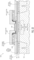
- Figure 1 is a partial cutaway side view of a wafer 101 according to one embodiment of the present invention.
- Wafer 101 includes a substrate layer 103 of monocrystalline silicon (Mono Silicon).
- a collector well 108 is laterally located between portions of a shallow trench isolation structure (STI) 105.
- STI 105 laterally surrounds well 108.
- well 108 is doped with N type conductivity dopants (e.g., arsenic, phosphorous) but may be doped with P type conductivity dopants (Boron) in other embodiments.
- N type conductivity dopants e.g., arsenic, phosphorous
- P type conductivity dopants Billoron
- a semiconductor layer 104 is located on STI 105 and collector well 108.
- layer 104 is made of silicon and serves as a seed layer for the formation of a subsequent semiconductor layer 106.
- layer 104 is formed by a non selective epitaxial growth process such that a portion 111 (EPI MONO SILICON) of layer 104 formed over mono crystalline silicon well 108 has a monocrystalline structure with an initial lattice constant generally matching that of well 108.
- a second portion 109 (EPI POLY SILICON) formed over the oxide of STI 105 has a polycrystalline structure.
- Semiconductor layer 106 is formed over layer 104.
- layer 106 is formed by a non selective epitaxial growth process of silicon germanium.
- portion 115 of layer 106 is monocrystalline with a lattice constant initially matching that of the top portion of portion 111 of layer 104.
- portion 113 is grown on polycrystalline portion 109 of layer 104, portion 113 has a polycrystalline structure.
- layer 106 is doped in-situ with a P type conductivity dopants (e.g., Boron), but may be doped after deposition by an ion implantation process in other embodiments.
- P type conductivity dopants e.g., Boron
- a middle portion of layer 106 would be doped insitu with P-type conductivity dopants.
- Portion 115 will include the intrinsic base for a subsequently formed transistor.
- layer 106 has a thickness in the range of 15-30nm but may have other thicknesses in other embodiments.
- An oxide pad 119 is formed on selected portions of layer 106.
- pad 119 is formed by a low pressure chemical vaper deposition (LPCVD) process or a plasma enhanced chemical vapor deposition (PECVD) blanket deposition process where the formed layer has a thickness in a range 5-20nm, but may have other thicknesses or be formed by other processes in other embodiments.
- LPCVD low pressure chemical vaper deposition
- PECVD plasma enhanced chemical vapor deposition
- a photoresist layer (not shown) is formed and patterned to form a mask to pattern the oxide layer to form pad 119. Afterwards, the photoresist mask is removed.
- Figure 1 also shows wafer 101 after a selectively implanted collector (SIC) region 121 is formed by an ion implantation of N-type dopants prior to the formation of SiGe layer 106.
- region 121 is formed by the ion implantation of N-type conductivity dopants at a dosage of 2e13-2e14 per cm 3 and at energies in the range of 100-500keV, but may be formed with other dosages and at other energies in other embodiments.
- Region 121 serves as a collector region for a subsequently formed transistor. In other embodiments, collector region 121 may be formed during other subsequent stages of manufacture.
- wafer 101 may have other configurations, include other layers, be made of other materials, and/or be formed by other methods.
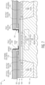
- Figure 2 is a partial cutaway side view of a wafer 101 after a layer of poly silicon 201 is selectively grown on portion 113.
- Layer 201 has a similar thickness as pad 119.
- a blanket layer of poly silicon (not shown) may be deposited on wafer 101 where wafer 101 is planarized using pad 119 as an etch stop.
- Figure 3 is a partial cutaway side view of a wafer 101 after a layer of oxide 301 is deposited on layer 201 and pad 119.
- layer 301 has a thickness of 20 nm, but may be of other thicknesses in other embodiments.
- a layer of poly silicon 303 is formed on layer 301, followed by a layer of Nitride layer 305.
- Figure 4 is a partial cutaway side view of wafer 101 after an emitter widow opening 401 is formed in layers 305 and 303 to expose oxide layer 301.
- opening 401 is formed by a timed reactive ion etch (RIE) through an opening in a patterned photoresist mask (not shown).
- RIE reactive ion etch
- opening 401 may be formed by other ways in other embodiments.
- opening 401 is formed in an area of wafer 101 that is located between STI 105 portions shown in Figure 4 .
- Figure 5 is a partial cutaway side view of wafer 101 after the pattern photo resist mask (not shown) is removed and layer 301 and pad 119 are isotropically (wet) etched to expose SiGe portion 115 and to etch back layer 301 and pad 119 past the edge of patterned nitride layer 305 and poly silicon layer 303 at location 501.
- layer 301 and pad 119 would be first anisotropically etched to expose portion 115 followed by an isotropic timed etch to remove the portions of layer 301 and pad 119 at location 501.
- Figure 6 is a partial cutaway side view of wafer 101 after the etched back sidewalls of pad 119 and oxide layer 301 are sealed with silicon 601.
- silicon 601 is formed by subjecting wafer 101 to a low temperature anneal in a hydrogen ambient, facilitating silicon atom mobility from layer 303 and SiGe portion 115 to seal exposed portions of pad 119 and layer 301.
- Figure 7 is a partial cutaway side view of wafer 101 after the formation of an emitter window spacer 701.
- spacer 701 is formed on the inside walls of the emitter window opening 401.
- spacer 701 is shown as two sperate portions.
- spacer 701 is contiguous around the entire perimeter of emitter window opening 401.
- the bottom of spacer 701 further narrows the emitter window to narrow the contact area between the intrinsic base portion 115 and a subsequently formed monocrystalline emitter portion 803 in Figure 8 .
- spacer 701 includes a thin layer of nitride located over a thin layer of oxide.
- spacer 701 is formed by forming an initial thin oxide layer, followed by forming a thin nitride layer, and then followed by forming a subsequent oxide layer (not shown). Afterwards, a poly silicon spacer (not shown) is formed to define the width of the bottom opening in spacer 701 were the oxide-nitride-oxide layers are etched using the poly silicon spacer as a mask.
- the subsequent oxide layer is anisotropically etch to form an oxide spacer (not shown) that is then used to anisotropically etch the thin nitride layer, which is then used to etch (isotropically, anisotropically, or by a combination) the initial thin oxide layer, where the initial oxide layer and the nitride layer make up spacer 701.
- the oxide spacer of the subsequent oxide layer is removed during subsequent processing (e.g., during an HF acid clean before the emitter material deposition), although it may remain in some embodiments.
- a spacer 701 may be formed by other ways. Some embodiments may not include spacer 701.
- Figure 8 is a partial cutaway side view of wafer 101 after the formation of a silicon electrode layer 800.
- layer 800 is grown by an epitaxial process where portion 801 is poly silicon and portion 803 (which is located over the opening in spacer 701) is monocrystalline. Portion 803 will serve as the intrinsic electrode for the transistor.
- Figure 9 is a partial cutaway side view of wafer 101 after polysilicon portion 801, nitride layer 305, polysilicon layer 303 and oxide layer 301 are patterned to expose polysilicon layer 201. In one embodiment, these layers are patterned through a patterned photoresist mask (not shown) using a reactive ion etch (RIE).
- RIE reactive ion etch
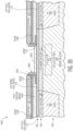
- Figure 10 is a partial cutaway side view of wafer 101 after oxide layer 301 and pad 119 have been etched with an isotropic etch.
- the removal of oxide layer 301 and pad 119 exposes portions of poly silicon layer 201, poly silicon layer 201, silicon 601, and monocrystalline base portion 115.
- Silicon 601 prevents the oxide of spacer 701 from being etched during the removal of the oxide.
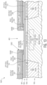
- Figure 11 is a partial cutaway side view of wafer 101 after a layer of cobalt 1101 has been deposited on the exposed surfaces of wafer 101.
- the cobalt is deposited on the surfaces that were exposed by the removal of oxide layer 301 and pad 119 (as shown in the view of Figure 10 ).
- the cobalt is deposited using a chemical vapor deposition (CVD) process.
- CVD chemical vapor deposition
- other metals used for silicidation e.g., tungsten, platinum, nickel
- tungsten, platinum, nickel may be deposited.
- Figure 12 is a partial cutaway side view of wafer 101 after wafer 101 has been annealed at a high temperature where the deposited cobalt 1101 as shown in Figure 11 is reacted with any exposed semiconductor material that includes silicon to form a layer of cobalt silicide on those surfaces. The unreacted cobalt is then removed.
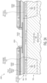
- a base silicide 1201 is formed on poly silicon layer 201, poly silicon layer 303, silicon 601, and on monocrystalline SiGe base portion 115.
- An emitter silicide 1203 is formed on portion poly silicon portion 801 and mono silicon portion 803 of the emitter electrode.
- Figure 12 also shows wafer 101 after one of more layers of dielectric material 1205 are formed on wafer 101. Openings are then formed in material 1205 to expose the silicide structures (e.g., silicides 1201 and 1203). Contact metal (e.g., tungsten, titanium, and/or titanium nitride) is then formed in the openings where wafer 101 is planarized to form the contacts for the electrodes of wafer 101. For example, base contacts 1207 and 1208 (contact on right side of wafer 101) are formed to contact base silicide 1201 and emitter contact 1209 is formed to contact emitter silicide 1203.
- silicide structures e.g., silicides 1201 and 1203
- Contact metal e.g., tungsten, titanium, and/or titanium nitride
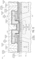
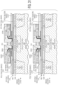
- Figure 12 shows a cross section of a HBT bipolar transistor with an emitter that includes an intrinsic emitter of N type doped portion 803 and emitter portion 801.
- the bipolar transistor includes a base including a P-type doped intrinsic base 1221 in mono SiGe base layer portion 115, poly SiGe portion 113, poly silicon layer 201, and poly silicon layer 303.
- the transistor also includes a collector including region 121 located in collector well 108.
- base contacts 1207 and 1208 electrically contact base silicide 1201.
- Base silicide 1201 provides an electrical path from the base contacts to monocrystalline SiGe layer portion 115 (which includes a boron doping) which includes the intrinsic base 1221 that is directly between intrinsic emitter portion 803 and collector region 121.
- a sacrificial material e.g., the oxide of pad 119
- the contact for the collector is not shown in the cutaway view of Figure 12 .
- wafer 101 After the stage of manufacture shown in Figure 12 , subsequent processes may be performed on wafer 101.
- upper interconnect layers (not shown) may be formed on top of wafer 101 and include conductive structures electrically coupled to the contacts for the collector, emitter, and/or base of the transistor of Figure 12 as well as to the contacts of other devices formed on wafer 101.
- wafer 101 is separated into multiple semiconductor dies each with at least one transistor similar to the transistor shown in Figure 12 .
- the die are protected in semiconductor packages that can be implemented in electronic systems such as e.g., RF communications devices, motor controllers, automotive electronics systems, or cellular phones.
- the transistor is used as a power amplifier to amplify a received RF signal or to amplify an RF signal to be transmitted, for example, as used in a cellular telephone.
- Figure 13 is a cutaway side view of a wafer 1301 during a stage in the manufacturer of a transistor according to another embodiment.
- the stage shown in Figure 13 shows an alternative embodiment to some of the processes of Figures 1-12 , where structures having the same reference numbers are similar.
- Figure 13 is a subsequent stage to the stage of Figure 4 and shows an alternative process for sealing the oxide material from the emitter window opening 401.
- oxide layer 301 and pad 119 are anisotropically etched through emitter window 401 to expose layer portion 115.
- a nitride spacer 1303 is formed on the side wall of opening 401 by the deposition of a thin nitride layer and a timed anisotropic etch of the nitride layer to expose layer portion 115.
- Nitride spacer 1303 seals oxide layer 301 and pad 119.
- the processes shown and described subsequent to Figure 6 are performed on wafer 101.
- nitride spacer 1303 for sealing the sacrificial oxide do not include polysilicon layer 303, wherein the nitride layer 305 would be formed on oxide layer 301. Also in some embodiments, oxide layer 301 and pad 119 may be isotropically etched to be set back the edges of those structures from the sidewall of opening 401.
- Figures 14-23 are partial cutaway side views of a wafer during various stages in the manufacture of a transistor according to another embodiment of the present invention. Structures with the same references numbers as with earlier described embodiments are similar.
- Figure 14 is a partial cutaway side view of wafer 1401 at a stage in the manufacture of a transistor.
- Figure 14 is subsequent to the stage shown in Figure 1 .
- a poly silicon base layer 1403 is formed on wafer 1401 over layer 106 and oxide pad 119.
- An oxide layer 1405 is formed on layer 1403 and a nitride layer 1407 is formed on oxide layer 1405.
- Figure 15 is a partial cutaway side view of wafer 1401 after an emitter window opening 401 is formed in wafer 1401 to expose oxide pad 119.
- Figure 16 is a partial cutaway side view of wafer 1401 after an oxide sidewall spacer 1601 is formed on the side wall of emitter window 401.
- spacer 1601 is formed by the deposition of an oxide layer on wafer 1401 and an anisotropic etching of the oxide layer.
- the width of spacer 1601 is the same as the thickness of oxide layer 1405.
- spacer 1601 has a width of 10 nm, but may be of other widths in other embodiments.
- Figure 17 is a partial cutaway side view of wafer 1401 after a sacrificial plug is 1701 is formed in emitter opening 401 and spacer 1601 is etched to reduce the height of the spacer.
- plug 1701 is formed by the deposition of poly silicon followed by a timed etch to reduce the top of plug 1701 below the height of nitride layer 1407.
- a chemical mechanical polish process may be used in conjunction with a timed etch to recess the top of plug 1701. Afterwards, wafer 1401 is subjected to an anisotropic etch to remove a top portion of spacer 1601.
- Figure 18 is a partial cutaway side view of wafer 1401 after a nitride sidewall spacer 1801 is formed on the sidewall of emitter window 401 after the removal of plug 1701.
- spacer 1801 is formed by depositing a layer of nitride (not shown) followed by an anisotropic etch of the nitride layer to expose pad 119.
- spacer 1801 has a width of 15 nm, but may be of other widths in other embodiments.
- Figure 19 is a partial cutaway side view of wafer 1401 after wafer 1401 has been subjected to a timed wet etch to remove a portion of pad 119. As shown in Figure 19 , a portion of pad 119 located directly beneath spacer 1801 at location 1901 is removed to set back pad from the exposed sidewall of spacer 1801.
- Figure 20 is a partial cutaway side view of wafer 1401 after a sealing process is performed to form a silicon capping layer 2001 on portion 115.
- caping layer 2001 is formed by a selective epitaxial growth process where cap layer 2001 is a monocrystalline silicon layer. Cap layer 2001 is grown to a level that is just above the bottom of spacer 1801 to seal the oxide of pad 119 and spacer 1601.
- Figure 21 is a partial cutaway side view of wafer 1401 after emitter window spacer 701, intrinsic mono silicon emitter portion 803, and poly silicon emitter electrode portion 801 are formed and portion 801 is patterned (along with nitride layer 1407 and oxide layer 1405) to form an emitter electrode. See the discussion of Figures 8 and 9 above regarding the formation of these structures. As a result of the patterning of portion 801, layer 1407, and layer 1405, portions of base poly silicon layer 1403 are exposed.
- Figure 22 is a partial cutaway side view of wafer 1401 after wafer 1401 is subject to an isotropic etch to remove the oxide material from pad 119, oxide spacer 1601, and oxide layer 1405. As a result of the etch, a surface on mono SiGe portion 115 is exposed.
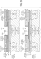
- Figure 23 is a partial cutaway side view of wafer 1401 after emitter silicide 1203 and base silicide 2301 are formed on the exposed surfaces of wafer 1401 that contain silicon.
- base silicide 2301 is formed on a top, side and bottom surfaces of poly base layer 1403 and on a top surface of mono SiGe portion 115.
- a cavity 2303 is formed at some locations where the oxide of pad 119, oxide spacer 1601, and oxide layer 1405 were removed.
- Figure 23 also shows wafer 1401 after dielectric material 1205 is formed. After the formation of dielectric material 1205, base contacts 1207 and 1208 are formed to electrically contact base silicide 2301 and emitter contact 1209 is formed to electrically contact emitter silicide 1203. See the discussion above regarding Figures 11-12 for further details on the formation of silicides and contacts. Afterwards, further processes may be performed on wafer 1401.
- Figures 24-26 are a partial cutaway side views of a wafer 2401 during stages in its manufacturer according to another embodiment.
- the stages of Figures 24-26 shows an alternative embodiment to processes of Figures 14-23 where structures having the same references numbers as earlier embodiments are similar.
- Figures 24-26 are subsequent stages to the stage of Figure 17 and show an alternative process for sealing the oxide material from the emitter window opening 401.
- a polysilicon spacer 2403 is formed on wafer 2401.
- Spacer 2403 is formed by depositing a layer of poly silicon (not shown) on wafer 2401 followed by an anisotropical etch of the layer.
- wafer 2401 is subject to an isotropic etch to remove a portion of pad 119 including at location 2501 under spacer 2403.
- Figure 26 shows where semiconductor material 2603 is formed by subjecting wafer 2401 to a low temperature anneal in a hydrogen ambient, facilitating silicon atom mobility from spacer 2403 and SiGe portion 115 to seal exposed portions of pad 119. Afterwards, other processer may be formed on wafer 2401 including the formation of a base silicide at the location of pad 119. See the discussion above regarding the previous embodiments for further processes.
- Figures 27-32 show various stages in the manufacture of a transistor according to another embodiment of the present invention.
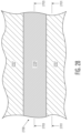
- Figure 27 shows two different partial cutaway side views (cross sections 2701 and 2703) of wafer 2700.
- Figure 28 shows a top view of wafer 2700 showing the locations of cross section 2701 and 2703.
- Figure 27 shows a stage in manufacture of a transistor that occurs after the stage in Figure 1 . Structures having the same references numbers are similar to those is previous embodiments.
- a polysilicon base layer 2707 is deposited over wafer 2700 including over layer 106 and oxide pad 119.
- a patterned trench is selectively formed in a region of layer 2707 that includes the location of cross section 2703.
- the trench is then filled with oxide and planarized to form oxide layer 2709. See Figure 28 for the location of the trench as shown by the location of oxide layer 2709.
- the trench may contact pad 119 wherein oxide layer 2709 would contact pad 119 after oxide fill.
- Figure 29 shows a stage after an emitter window 411 is formed to expose pad 119 and after an oxide sidewall spacer 2903 is formed on the side of the emitter window 411. Oxide spacer contacts oxide layer 2709 in cross section 2703.
- Figure 30 shows wafer 2700 after spacer 2903 has been reduced in height and poly spacer 3001 is formed to cover spacer 2903. Afterwards, a portion of pad 119 is removed. Silicon material 3007 is formed below spacer 3001 to seal oxide spacer 2903 and pad 119. Silicon material 3007 is formed below spacer 3001 by subjecting wafer 2700 to a low temperature anneal in a hydrogen ambient, facilitating silicon atom mobility from spacer 3001 and SiGe portion 115 to seal exposed portions of pad 119. See the discussion above regarding Figures 24-26 for further details on this process.
- oxide spacer 2903 and the remaining portion of pad 119 may be sealed with a nitride spacer (see the discussion above regarding Figure 13 ) or by epitaxially growing a silicon cap layer (see the discussion of Figures 18-20 above).
- Figure 31 shows cross sections 2701 and 2703 after emitter window spacer 701, intrinsic mono silicon emitter portion 803, and poly silicon emitter electrode portion 801 are formed and portion 801 is patterned to form an emitter electrode. Patterned along with portion 801 are nitride layer 2901 and oxide layer 2709 (located in cross section 2703) to expose the top of poly silicon layer 2707. See the discussion above regarding the formation of these structures in earlier embodiments.
- Figure 32 shows cross sections 2701 and 2703 after wafer 2700 is subject to an isotropic etch to remove the exposed oxide material from pad 119, oxide spacer 2903, and oxide layer 2709 to form opening 3201. As a result of the etch, a surface on mono SiGe portion 115 is exposed.
- the portion of the opening 3201 formed in cross section 2703 from the removal of oxide layer 2709 allows for the portion of pad 119 and spacer 2903 to be removed in the portion of wafer 2700 that did not include layer 2709 as shown in Section 2701. In some embodiments, this may allow for a portion of the transistor to be formed without forming a "cantilever" emitter electrode/nitride portion of emitter portion 801 and nitride layer 2901 as shown in cross section 2703 from the removal of layer 2709. Providing a portion of the transistor without the cantilever structure may reduce the probability of structural breakage during subsequent wafer processing.
- a transistor may be made with multiple narrower trenches in poly silicon layer 2707 that are similar to the trench of oxide layer 2709 where the multiple trenches are spaced apart across the transistor to allow for access of the etchant to all parts of pad 119 and spacer 2903 for removal.
- silicide (not shown) is formed on all exposed silicon containing structures of wafer 2700 including on poly silicon base layer 2707 and portion 115 to form a base silicide and on emitter portions 801 and 803 to form an emitter silicide.
- a layer of dielectric material (not shown) is formed over wafer 2700, contacts (not shown) are made to the emitter silicide and base silicide. See Figures 11 and 12 above. Afterwards, further processes may be performed on wafer 2700.
- Forming trenches in the polysilicon layer and then depositing oxide in those trenches may be implemented in the other embodiments described herein such as with the embodiment of Figures 1-12 , the embodiment of Figure 13 , the embodiment of Figures 14-23 , and the embodiment of Figure 24-26 .
- providing processes that form a sacrificial layer such as an oxide on a mono crystalline base material may allow for the subsequent formation of a portion of a base silicide that that electrically contacts the mono crystalline base layer which contains the intrinsic emitter. This may allow for a silicided path from the base contact to the monocrystalline layer which lowers the resistance from the base contact to the intrinsic base.
- transistors describe herein may have other configurations, have other structures, be made of other materials, and/or may be made by other processes.
- Figures 12 and 23 each show an NPN bipolar transistor, however, other types of transistors may be made by the processes described herein.
- a PNP transistor may be formed where the collector and emitter have a net P-type conductivity doping and the base has a net N-type conductivity doping.
- a first structure is "directly over" a second structure if the first structure is located over the second structure in a line having a direction that is perpendicular with a generally planar major side of the wafer or substate.
- silicide 1203 is directly over silicide 1201.
- Portion 803 is not directly over STI 105.
- a first structure is "directly beneath” or “directly under” a second structure if the first structure is located beneath the second structure in a line having a direction that is perpendicular with a generally planar major side of the wafer or substrate.
- portion 111 is directly beneath silicide 1203.
- Portion 115 is not directly beneath contact 1207.
- One structure is “directly between” two other structures in a line if the two structures are located on opposite sides of the one structure in the line.
- nitride layer 305 is located directly between contacts 1207 and 1209 in a line in the cut away side view of Figure 12 .
- Collector region 121 is not located directly between contacts 1207 and 1208.
- a first structure is "directly lateral" to a second structure if the first structure and second structure are located in a line having a direction that is parallel with a generally planar major side of the wafer or substrate.
- emitter contact 1209 and base contact 1207 are directly lateral to each other.
- One structure is "directly laterally between” two other structures if the two structures are located on opposite sides of the one structure in a line that is parallel with a generally planar major side of the wafer or substrate.
- nitride layer 305 is located directly laterally between base contact 1207 and emitter contact 1209.
- a surface is at a "higher elevation” than another surface, if that surface is located closer to the top of the active side of a wafer or die in a line having a direction that is perpendicular with the generally planar major side of the wafer or die.
- the active side of the wafer is the top side of the Figures.
- contact 1209 is at a higher elevation than portion 115.
- a method for forming a transistor includes forming a collector of a transistor and forming a base of the transistor.
- the base includes a monocrystalline base layer.
- the method includes forming an emitter of the transistor, forming a sacrificial material in contact with the monocrystalline base layer, removing at least a portion of the sacrificial material, and forming a base silicide.
- the forming the base silicide includes forming at least a portion of the base silicide on a portion of the monocrystalline base layer exposed by the removing.
- Forming an emitter silicide on the emitter may, according to one or more embodiment, be simultaneous with forming the base silicide.
- a method of forming a transistor includes forming a sacrificial material over a monocrystalline base layer, forming an emitter electrode material over sacrificial material, and patterning the emitter electrode material to form a patterned emitter structure.
- the method includes after the patterning the emitter electrode material, removing the sacrificial material from at least a portion of the monocrystalline base layer.
- the method includes forming a base silicide.
- the forming the base silicide includes forming at least a portion of the base silicide on a portion of the monocrystalline base layer exposed by the removing.
- the patterned emitter structure is located directly over at least a portion of the portion of the monocrystalline base layer exposed by the removing.
Landscapes
- Bipolar Transistors (AREA)
Abstract
Description
- This invention relates in general to transistors with base structures.
- Some transistors such as bipolar transistors include a base as one of the transistor electrodes. Some types of bipolar transistors, such as heterojunction bipolar transistors (HBTs) can be used for high speed switching applications. HBTs typically implement different semiconductor material types for the emitter and base regions, creating a heterojunction. Some HBTs can handle signals of very high frequencies, up to several hundred GHz. HBTs can be used in radio-frequency (RF) systems and in applications requiring high power efficiency, such as in RF power amplifiers for cellular phones.
- The present invention may be better understood, and its numerous objects, features, and advantages made apparent to those skilled in the art by referencing the accompanying drawings.
-
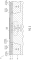
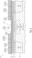
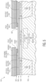
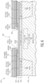
Figures 1-12 are partial cutaway side views of a wafer during various stages in the manufacture of a semiconductor device according to one embodiment of the present invention. -
Figure 13 is a partial cutaway side view of a wafer at a stage in the manufacture of a semiconductor device according to another embodiment of the present invention. -
Figures 14-23 are partial cutaway side views of a wafer during various stages in the manufacture of a semiconductor device according to another embodiment of the present invention. -
Figures 24-26 are partial cutaway side views of a wafer during various stages in the manufacture of a semiconductor device according to another embodiment of the present invention. -
Figures 27 and29-32 are partial cutaway side views andFigure 28 is a top view of a wafer during various stages in the manufacture of a semiconductor device according to another embodiment of the present invention. - The use of the same reference symbols in different drawings indicates identical items unless otherwise noted. The Figures are not necessarily drawn to scale.
- The following sets forth a detailed description of at least one mode for carrying out the invention. The description is intended to be illustrative of the invention and should not be taken to be limiting.
- Disclosed herein is a transistor with an emitter, base, and collector. The base includes a monocrystalline base layer. A sacrificial material is formed on the monocrystalline base layer. The sacrificial material is removed to expose a portion of the monocrystalline base layer. A base silicide includes a portion formed on the portion of the base monocrystalline base layer that was exposed by the removal of the sacrificial material.
- In some embodiments, forming a transistor by forming a sacrificial material over a monocrystalline base layer and then removing the sacrificial material to expose a portion of the monocrystalline base layer for the formation of a silicide on the monocrystalline base layer may provide for a transistor with a low resistance from a base contact to the intrinsic base region in that the base silicide may be located closer to the intrinsic base region.
- Some transistors such as HBTs use polycrystalline silicon (poly silicon) for an extrinsic base material. This provides for a conductivity path from the base contact through the base silicide and the extrinsic poly silicon to the intrinsic base which is located in a layer of monocrystalline (mono) semiconductor material. The polysilicon utilized for the extrinsic base material may lead to a higher resistance of this path. Accordingly providing a method where a portion of the base silicide can be formed on the base monocrystalline silicon material may reduce the resistance of the path to the base contact.
-
Figure 1 is a partial cutaway side view of awafer 101 according to one embodiment of the present invention. Wafer 101 includes asubstrate layer 103 of monocrystalline silicon (Mono Silicon). Acollector well 108 is laterally located between portions of a shallow trench isolation structure (STI) 105. In one embodiment, STI 105 laterally surrounds well 108. In one embodiment, well 108 is doped with N type conductivity dopants (e.g., arsenic, phosphorous) but may be doped with P type conductivity dopants (Boron) in other embodiments. - A
semiconductor layer 104 is located on STI 105 andcollector well 108. In one embodiment,layer 104 is made of silicon and serves as a seed layer for the formation of asubsequent semiconductor layer 106. In one embodiment, after a cleaning operation with HF acid and a pre-bake in a hydrogen atmosphere,layer 104 is formed by a non selective epitaxial growth process such that a portion 111 (EPI MONO SILICON) oflayer 104 formed over monocrystalline silicon well 108 has a monocrystalline structure with an initial lattice constant generally matching that of well 108. A second portion 109 (EPI POLY SILICON) formed over the oxide ofSTI 105 has a polycrystalline structure. -
Semiconductor layer 106 is formed overlayer 104. In one embodiment, after an HF cleaning process and a hydrogen pre bake ofwafer 101 are performed,layer 106 is formed by a non selective epitaxial growth process of silicon germanium. As a result of the epitaxial growth process,portion 115 oflayer 106 is monocrystalline with a lattice constant initially matching that of the top portion ofportion 111 oflayer 104. Becauseportion 113 is grown onpolycrystalline portion 109 oflayer 104,portion 113 has a polycrystalline structure. In one embodiment,layer 106 is doped in-situ with a P type conductivity dopants (e.g., Boron), but may be doped after deposition by an ion implantation process in other embodiments. In some embodiment, a middle portion oflayer 106 would be doped insitu with P-type conductivity dopants.Portion 115 will include the intrinsic base for a subsequently formed transistor. In one embodiment,layer 106 has a thickness in the range of 15-30nm but may have other thicknesses in other embodiments. - An
oxide pad 119 is formed on selected portions oflayer 106. In one embodiment,pad 119 is formed by a low pressure chemical vaper deposition (LPCVD) process or a plasma enhanced chemical vapor deposition (PECVD) blanket deposition process where the formed layer has a thickness in a range 5-20nm, but may have other thicknesses or be formed by other processes in other embodiments. After the formation of the oxide layer, a photoresist layer (not shown) is formed and patterned to form a mask to pattern the oxide layer to formpad 119. Afterwards, the photoresist mask is removed. -
Figure 1 also showswafer 101 after a selectively implanted collector (SIC)region 121 is formed by an ion implantation of N-type dopants prior to the formation ofSiGe layer 106. In one embodiment,region 121 is formed by the ion implantation of N-type conductivity dopants at a dosage of 2e13-2e14 per cm3 and at energies in the range of 100-500keV, but may be formed with other dosages and at other energies in other embodiments.Region 121 serves as a collector region for a subsequently formed transistor. In other embodiments,collector region 121 may be formed during other subsequent stages of manufacture. - In other embodiments,
wafer 101 may have other configurations, include other layers, be made of other materials, and/or be formed by other methods. -
Figure 2 is a partial cutaway side view of awafer 101 after a layer ofpoly silicon 201 is selectively grown onportion 113.Layer 201 has a similar thickness aspad 119. In other embodiments, a blanket layer of poly silicon (not shown) may be deposited onwafer 101 wherewafer 101 is planarized usingpad 119 as an etch stop. -
Figure 3 is a partial cutaway side view of awafer 101 after a layer ofoxide 301 is deposited onlayer 201 andpad 119. In one embodiment,layer 301 has a thickness of 20 nm, but may be of other thicknesses in other embodiments. Afterwards, a layer ofpoly silicon 303 is formed onlayer 301, followed by a layer of Nitridelayer 305. -
Figure 4 is a partial cutaway side view ofwafer 101 after anemitter widow opening 401 is formed inlayers oxide layer 301. In one embodiment, opening 401 is formed by a timed reactive ion etch (RIE) through an opening in a patterned photoresist mask (not shown). However, opening 401 may be formed by other ways in other embodiments. In the embodiment shown, opening 401 is formed in an area ofwafer 101 that is located betweenSTI 105 portions shown inFigure 4 . -
Figure 5 is a partial cutaway side view ofwafer 101 after the pattern photo resist mask (not shown) is removed andlayer 301 andpad 119 are isotropically (wet) etched to exposeSiGe portion 115 and to etch backlayer 301 and pad 119 past the edge of patternednitride layer 305 andpoly silicon layer 303 atlocation 501. In one embodiment,layer 301 andpad 119 would be first anisotropically etched to exposeportion 115 followed by an isotropic timed etch to remove the portions oflayer 301 and pad 119 atlocation 501. -
Figure 6 is a partial cutaway side view ofwafer 101 after the etched back sidewalls ofpad 119 andoxide layer 301 are sealed withsilicon 601. In one embodiment,silicon 601 is formed by subjectingwafer 101 to a low temperature anneal in a hydrogen ambient, facilitating silicon atom mobility fromlayer 303 andSiGe portion 115 to seal exposed portions ofpad 119 andlayer 301. -
Figure 7 is a partial cutaway side view ofwafer 101 after the formation of anemitter window spacer 701. In one embodiment,spacer 701 is formed on the inside walls of theemitter window opening 401. In the cross-sectional view ofFigure 7 ,spacer 701 is shown as two sperate portions. However, for the embodiment ofFigure 7 ,spacer 701 is contiguous around the entire perimeter ofemitter window opening 401. The bottom ofspacer 701 further narrows the emitter window to narrow the contact area between theintrinsic base portion 115 and a subsequently formedmonocrystalline emitter portion 803 inFigure 8 . - In the embodiment shown,
spacer 701 includes a thin layer of nitride located over a thin layer of oxide. In one embodiment,spacer 701 is formed by forming an initial thin oxide layer, followed by forming a thin nitride layer, and then followed by forming a subsequent oxide layer (not shown). Afterwards, a poly silicon spacer (not shown) is formed to define the width of the bottom opening inspacer 701 were the oxide-nitride-oxide layers are etched using the poly silicon spacer as a mask. The subsequent oxide layer is anisotropically etch to form an oxide spacer (not shown) that is then used to anisotropically etch the thin nitride layer, which is then used to etch (isotropically, anisotropically, or by a combination) the initial thin oxide layer, where the initial oxide layer and the nitride layer make upspacer 701. The oxide spacer of the subsequent oxide layer is removed during subsequent processing (e.g., during an HF acid clean before the emitter material deposition), although it may remain in some embodiments. In other embodiments, aspacer 701 may be formed by other ways. Some embodiments may not includespacer 701. -
Figure 8 is a partial cutaway side view ofwafer 101 after the formation of asilicon electrode layer 800. In one embodiment,layer 800 is grown by an epitaxial process whereportion 801 is poly silicon and portion 803 (which is located over the opening in spacer 701) is monocrystalline.Portion 803 will serve as the intrinsic electrode for the transistor. -
Figure 9 is a partial cutaway side view ofwafer 101 afterpolysilicon portion 801,nitride layer 305,polysilicon layer 303 andoxide layer 301 are patterned to exposepolysilicon layer 201. In one embodiment, these layers are patterned through a patterned photoresist mask (not shown) using a reactive ion etch (RIE). -
Figure 10 is a partial cutaway side view ofwafer 101 afteroxide layer 301 and pad 119 have been etched with an isotropic etch. The removal ofoxide layer 301 andpad 119 exposes portions ofpoly silicon layer 201,poly silicon layer 201,silicon 601, andmonocrystalline base portion 115.Silicon 601 prevents the oxide ofspacer 701 from being etched during the removal of the oxide. -
Figure 11 is a partial cutaway side view ofwafer 101 after a layer ofcobalt 1101 has been deposited on the exposed surfaces ofwafer 101. As shown inFigure 11 , the cobalt is deposited on the surfaces that were exposed by the removal ofoxide layer 301 and pad 119 (as shown in the view ofFigure 10 ). In one embodiment, the cobalt is deposited using a chemical vapor deposition (CVD) process. However, in other embodiment, other metals used for silicidation (e.g., tungsten, platinum, nickel) may be deposited. -
Figure 12 is a partial cutaway side view ofwafer 101 afterwafer 101 has been annealed at a high temperature where the depositedcobalt 1101 as shown inFigure 11 is reacted with any exposed semiconductor material that includes silicon to form a layer of cobalt silicide on those surfaces. The unreacted cobalt is then removed. InFigure 12 , abase silicide 1201 is formed onpoly silicon layer 201,poly silicon layer 303,silicon 601, and on monocrystallineSiGe base portion 115. Anemitter silicide 1203 is formed on portionpoly silicon portion 801 andmono silicon portion 803 of the emitter electrode. -
Figure 12 also showswafer 101 after one of more layers ofdielectric material 1205 are formed onwafer 101. Openings are then formed inmaterial 1205 to expose the silicide structures (e.g.,silicides 1201 and 1203). Contact metal (e.g., tungsten, titanium, and/or titanium nitride) is then formed in the openings wherewafer 101 is planarized to form the contacts for the electrodes ofwafer 101. For example,base contacts 1207 and 1208 (contact on right side of wafer 101) are formed to contactbase silicide 1201 andemitter contact 1209 is formed to contactemitter silicide 1203. - Accordingly,
Figure 12 shows a cross section of a HBT bipolar transistor with an emitter that includes an intrinsic emitter of N type dopedportion 803 andemitter portion 801. The bipolar transistor includes a base including a P-type dopedintrinsic base 1221 in mono SiGebase layer portion 115,poly SiGe portion 113,poly silicon layer 201, andpoly silicon layer 303. The transistor also includes acollector including region 121 located in collector well 108. - As shown in
Figure 12 ,base contacts contact base silicide 1201.Base silicide 1201 provides an electrical path from the base contacts to monocrystalline SiGe layer portion 115 (which includes a boron doping) which includes theintrinsic base 1221 that is directly betweenintrinsic emitter portion 803 andcollector region 121. Accordingly, providing a process where a sacrificial material (e.g., the oxide of pad 119) that is formed in contact with the mono base portion (115) and removed to form a silicide, may provide the transistor ofFigure 12 with a silicided path to lower the base biasing resistance fromcontacts intrinsic base 1221. The contact for the collector is not shown in the cutaway view ofFigure 12 . - After the stage of manufacture shown in
Figure 12 , subsequent processes may be performed onwafer 101. For example, upper interconnect layers (not shown) may be formed on top ofwafer 101 and include conductive structures electrically coupled to the contacts for the collector, emitter, and/or base of the transistor ofFigure 12 as well as to the contacts of other devices formed onwafer 101. Afterwards,wafer 101 is separated into multiple semiconductor dies each with at least one transistor similar to the transistor shown inFigure 12 . The die are protected in semiconductor packages that can be implemented in electronic systems such as e.g., RF communications devices, motor controllers, automotive electronics systems, or cellular phones. In one example, the transistor is used as a power amplifier to amplify a received RF signal or to amplify an RF signal to be transmitted, for example, as used in a cellular telephone. -
Figure 13 is a cutaway side view of awafer 1301 during a stage in the manufacturer of a transistor according to another embodiment. The stage shown inFigure 13 shows an alternative embodiment to some of the processes ofFigures 1-12 , where structures having the same reference numbers are similar.Figure 13 is a subsequent stage to the stage ofFigure 4 and shows an alternative process for sealing the oxide material from theemitter window opening 401. In the embodiment ofFigure 13 , after the stage ofFigure 4 ,oxide layer 301 andpad 119 are anisotropically etched throughemitter window 401 to exposelayer portion 115. Afterwards, anitride spacer 1303 is formed on the side wall of opening 401 by the deposition of a thin nitride layer and a timed anisotropic etch of the nitride layer to exposelayer portion 115.Nitride spacer 1303seals oxide layer 301 andpad 119. Afterwards, the processes shown and described subsequent toFigure 6 (with respect to the embodiment ofFigures 1-12 ) are performed onwafer 101. - Some embodiments using a
nitride spacer 1303 for sealing the sacrificial oxide do not includepolysilicon layer 303, wherein thenitride layer 305 would be formed onoxide layer 301. Also in some embodiments,oxide layer 301 andpad 119 may be isotropically etched to be set back the edges of those structures from the sidewall ofopening 401. -
Figures 14-23 are partial cutaway side views of a wafer during various stages in the manufacture of a transistor according to another embodiment of the present invention. Structures with the same references numbers as with earlier described embodiments are similar. -
Figure 14 is a partial cutaway side view ofwafer 1401 at a stage in the manufacture of a transistor.Figure 14 is subsequent to the stage shown inFigure 1 . After the stage ofFigure 1 , a polysilicon base layer 1403 is formed onwafer 1401 overlayer 106 andoxide pad 119. Anoxide layer 1405 is formed onlayer 1403 and anitride layer 1407 is formed onoxide layer 1405. -
Figure 15 is a partial cutaway side view ofwafer 1401 after anemitter window opening 401 is formed inwafer 1401 to exposeoxide pad 119. -
Figure 16 is a partial cutaway side view ofwafer 1401 after anoxide sidewall spacer 1601 is formed on the side wall ofemitter window 401. In one embodiment,spacer 1601 is formed by the deposition of an oxide layer onwafer 1401 and an anisotropic etching of the oxide layer. In one embodiment, the width ofspacer 1601 is the same as the thickness ofoxide layer 1405. In one embodiment,spacer 1601 has a width of 10 nm, but may be of other widths in other embodiments. -
Figure 17 is a partial cutaway side view ofwafer 1401 after a sacrificial plug is 1701 is formed inemitter opening 401 andspacer 1601 is etched to reduce the height of the spacer. In one embodiment,plug 1701 is formed by the deposition of poly silicon followed by a timed etch to reduce the top ofplug 1701 below the height ofnitride layer 1407. In another embodiment, a chemical mechanical polish process may be used in conjunction with a timed etch to recess the top ofplug 1701. Afterwards,wafer 1401 is subjected to an anisotropic etch to remove a top portion ofspacer 1601. -
Figure 18 is a partial cutaway side view ofwafer 1401 after anitride sidewall spacer 1801 is formed on the sidewall ofemitter window 401 after the removal ofplug 1701. In one embodiment,spacer 1801 is formed by depositing a layer of nitride (not shown) followed by an anisotropic etch of the nitride layer to exposepad 119. In one embodiment,spacer 1801 has a width of 15 nm, but may be of other widths in other embodiments. -
Figure 19 is a partial cutaway side view ofwafer 1401 afterwafer 1401 has been subjected to a timed wet etch to remove a portion ofpad 119. As shown inFigure 19 , a portion ofpad 119 located directly beneathspacer 1801 atlocation 1901 is removed to set back pad from the exposed sidewall ofspacer 1801. -
Figure 20 is a partial cutaway side view ofwafer 1401 after a sealing process is performed to form asilicon capping layer 2001 onportion 115. In one embodiment,caping layer 2001 is formed by a selective epitaxial growth process wherecap layer 2001 is a monocrystalline silicon layer.Cap layer 2001 is grown to a level that is just above the bottom ofspacer 1801 to seal the oxide ofpad 119 andspacer 1601. -
Figure 21 is a partial cutaway side view ofwafer 1401 afteremitter window spacer 701, intrinsic monosilicon emitter portion 803, and poly siliconemitter electrode portion 801 are formed andportion 801 is patterned (along withnitride layer 1407 and oxide layer 1405) to form an emitter electrode. See the discussion ofFigures 8 and9 above regarding the formation of these structures. As a result of the patterning ofportion 801,layer 1407, andlayer 1405, portions of basepoly silicon layer 1403 are exposed. -
Figure 22 is a partial cutaway side view ofwafer 1401 afterwafer 1401 is subject to an isotropic etch to remove the oxide material frompad 119,oxide spacer 1601, andoxide layer 1405. As a result of the etch, a surface onmono SiGe portion 115 is exposed. -
Figure 23 is a partial cutaway side view ofwafer 1401 afteremitter silicide 1203 andbase silicide 2301 are formed on the exposed surfaces ofwafer 1401 that contain silicon. As shown inFigure 23 ,base silicide 2301 is formed on a top, side and bottom surfaces ofpoly base layer 1403 and on a top surface ofmono SiGe portion 115. In the embodiment shown, acavity 2303 is formed at some locations where the oxide ofpad 119,oxide spacer 1601, andoxide layer 1405 were removed. -
Figure 23 also showswafer 1401 afterdielectric material 1205 is formed. After the formation ofdielectric material 1205,base contacts contact base silicide 2301 andemitter contact 1209 is formed to electricallycontact emitter silicide 1203. See the discussion above regardingFigures 11-12 for further details on the formation of silicides and contacts. Afterwards, further processes may be performed onwafer 1401. -
Figures 24-26 are a partial cutaway side views of awafer 2401 during stages in its manufacturer according to another embodiment. The stages ofFigures 24-26 shows an alternative embodiment to processes ofFigures 14-23 where structures having the same references numbers as earlier embodiments are similar.Figures 24-26 are subsequent stages to the stage ofFigure 17 and show an alternative process for sealing the oxide material from theemitter window opening 401. - As shown in
Figure 24 , after the removal ofplug 1701 inFigure 17 , apolysilicon spacer 2403 is formed onwafer 2401.Spacer 2403 is formed by depositing a layer of poly silicon (not shown) onwafer 2401 followed by an anisotropical etch of the layer. - As shown in
Figure 25 ,wafer 2401 is subject to an isotropic etch to remove a portion ofpad 119 including atlocation 2501 underspacer 2403. -
Figure 26 shows wheresemiconductor material 2603 is formed by subjectingwafer 2401 to a low temperature anneal in a hydrogen ambient, facilitating silicon atom mobility fromspacer 2403 andSiGe portion 115 to seal exposed portions ofpad 119. Afterwards, other processer may be formed onwafer 2401 including the formation of a base silicide at the location ofpad 119. See the discussion above regarding the previous embodiments for further processes. -
Figures 27-32 show various stages in the manufacture of a transistor according to another embodiment of the present invention. -
Figure 27 shows two different partial cutaway side views (cross sections 2701 and 2703) ofwafer 2700.Figure 28 shows a top view ofwafer 2700 showing the locations ofcross section Figure 27 shows a stage in manufacture of a transistor that occurs after the stage inFigure 1 . Structures having the same references numbers are similar to those is previous embodiments. - After the stage of
Figure 1 , apolysilicon base layer 2707 is deposited overwafer 2700 including overlayer 106 andoxide pad 119. Afterwards, a patterned trench is selectively formed in a region oflayer 2707 that includes the location ofcross section 2703. The trench is then filled with oxide and planarized to formoxide layer 2709. SeeFigure 28 for the location of the trench as shown by the location ofoxide layer 2709. In some embodiments, the trench may contact pad 119 whereinoxide layer 2709 would contact pad 119 after oxide fill. -
Figure 29 shows a stage after anemitter window 411 is formed to exposepad 119 and after anoxide sidewall spacer 2903 is formed on the side of theemitter window 411. Oxide spacercontacts oxide layer 2709 incross section 2703. -
Figure 30 showswafer 2700 afterspacer 2903 has been reduced in height andpoly spacer 3001 is formed to coverspacer 2903. Afterwards, a portion ofpad 119 is removed.Silicon material 3007 is formed below spacer 3001 to sealoxide spacer 2903 andpad 119.Silicon material 3007 is formed belowspacer 3001 by subjectingwafer 2700 to a low temperature anneal in a hydrogen ambient, facilitating silicon atom mobility fromspacer 3001 andSiGe portion 115 to seal exposed portions ofpad 119. See the discussion above regardingFigures 24-26 for further details on this process. - In other embodiments,
oxide spacer 2903 and the remaining portion ofpad 119 may be sealed with a nitride spacer (see the discussion above regardingFigure 13 ) or by epitaxially growing a silicon cap layer (see the discussion ofFigures 18-20 above). -
Figure 31 showscross sections emitter window spacer 701, intrinsic monosilicon emitter portion 803, and poly siliconemitter electrode portion 801 are formed andportion 801 is patterned to form an emitter electrode. Patterned along withportion 801 arenitride layer 2901 and oxide layer 2709 (located in cross section 2703) to expose the top ofpoly silicon layer 2707. See the discussion above regarding the formation of these structures in earlier embodiments. -
Figure 32 showscross sections wafer 2700 is subject to an isotropic etch to remove the exposed oxide material frompad 119,oxide spacer 2903, andoxide layer 2709 to formopening 3201. As a result of the etch, a surface onmono SiGe portion 115 is exposed. - As shown in
Figure 32 , the portion of theopening 3201 formed incross section 2703 from the removal ofoxide layer 2709 allows for the portion ofpad 119 and spacer 2903 to be removed in the portion ofwafer 2700 that did not includelayer 2709 as shown inSection 2701. In some embodiments, this may allow for a portion of the transistor to be formed without forming a "cantilever" emitter electrode/nitride portion ofemitter portion 801 andnitride layer 2901 as shown incross section 2703 from the removal oflayer 2709. Providing a portion of the transistor without the cantilever structure may reduce the probability of structural breakage during subsequent wafer processing. - In some embodiments, a transistor may be made with multiple narrower trenches in
poly silicon layer 2707 that are similar to the trench ofoxide layer 2709 where the multiple trenches are spaced apart across the transistor to allow for access of the etchant to all parts ofpad 119 andspacer 2903 for removal. - After the stage of
Figure 32 , silicide (not shown) is formed on all exposed silicon containing structures ofwafer 2700 including on polysilicon base layer 2707 andportion 115 to form a base silicide and onemitter portions wafer 2700, contacts (not shown) are made to the emitter silicide and base silicide. SeeFigures 11 and12 above. Afterwards, further processes may be performed onwafer 2700. - Forming trenches in the polysilicon layer and then depositing oxide in those trenches may be implemented in the other embodiments described herein such as with the embodiment of
Figures 1-12 , the embodiment ofFigure 13 , the embodiment ofFigures 14-23 , and the embodiment ofFigure 24-26 . - As shown herein, providing processes that form a sacrificial layer such as an oxide on a mono crystalline base material may allow for the subsequent formation of a portion of a base silicide that that electrically contacts the mono crystalline base layer which contains the intrinsic emitter. This may allow for a silicided path from the base contact to the monocrystalline layer which lowers the resistance from the base contact to the intrinsic base.
- The transistors describe herein may have other configurations, have other structures, be made of other materials, and/or may be made by other processes. For example,
Figures 12 and23 each show an NPN bipolar transistor, however, other types of transistors may be made by the processes described herein. For example, a PNP transistor may be formed where the collector and emitter have a net P-type conductivity doping and the base has a net N-type conductivity doping. - As disclosed herein, a first structure is "directly over" a second structure if the first structure is located over the second structure in a line having a direction that is perpendicular with a generally planar major side of the wafer or substate. For example, in
Figure 12 ,silicide 1203 is directly oversilicide 1201.Portion 803 is not directly overSTI 105. As disclosed herein, a first structure is "directly beneath" or "directly under" a second structure if the first structure is located beneath the second structure in a line having a direction that is perpendicular with a generally planar major side of the wafer or substrate. For example, inFigure 12 ,portion 111 is directly beneathsilicide 1203.Portion 115 is not directly beneathcontact 1207. One structure is "directly between" two other structures in a line if the two structures are located on opposite sides of the one structure in the line. For example, inFigure 12 ,nitride layer 305 is located directly betweencontacts Figure 12 .Collector region 121 is not located directly betweencontacts emitter contact 1209 andbase contact 1207 are directly lateral to each other. One structure is "directly laterally between" two other structures if the two structures are located on opposite sides of the one structure in a line that is parallel with a generally planar major side of the wafer or substrate. For example, inFigure 12 ,nitride layer 305 is located directly laterally betweenbase contact 1207 andemitter contact 1209. A surface is at a "higher elevation" than another surface, if that surface is located closer to the top of the active side of a wafer or die in a line having a direction that is perpendicular with the generally planar major side of the wafer or die. In the views ofFigures 1-12 , the active side of the wafer is the top side of the Figures. For example,contact 1209 is at a higher elevation thanportion 115. - Features specifically shown or described with respect to one embodiment set forth herein may be implemented in other embodiments set forth herein. For example, the specific sealing processes disclosed with respect to one embodiment, may be implemented in another embodiment.
- In one embodiment, a method for forming a transistor includes forming a collector of a transistor and forming a base of the transistor. The base includes a monocrystalline base layer. The method includes forming an emitter of the transistor, forming a sacrificial material in contact with the monocrystalline base layer, removing at least a portion of the sacrificial material, and forming a base silicide. The forming the base silicide includes forming at least a portion of the base silicide on a portion of the monocrystalline base layer exposed by the removing.
- Forming an emitter silicide on the emitter may, according to one or more embodiment, be simultaneous with forming the base silicide.
- In another embodiment, a method of forming a transistor includes forming a sacrificial material over a monocrystalline base layer, forming an emitter electrode material over sacrificial material, and patterning the emitter electrode material to form a patterned emitter structure. The method includes after the patterning the emitter electrode material, removing the sacrificial material from at least a portion of the monocrystalline base layer. The method includes forming a base silicide. The forming the base silicide includes forming at least a portion of the base silicide on a portion of the monocrystalline base layer exposed by the removing. The patterned emitter structure is located directly over at least a portion of the portion of the monocrystalline base layer exposed by the removing.
- While particular embodiments of the present invention have been shown and described, it will be recognized to those skilled in the art that, based upon the teachings herein, further changes and modifications may be made without departing from this invention and its broader aspects, and thus, the appended claims are to encompass within their scope all such changes and modifications as are within the true spirit and scope of this invention.
Claims (15)
- A method for forming a transistor, the method comprising:forming a collector of a transistor;forming a base of the transistor, the base including a monocrystalline base layer;forming an emitter of the transistor;forming a sacrificial material in contact with the monocrystalline base layer;removing at least a portion of the sacrificial material;forming a base silicide, the forming the base silicide includes:
forming at least a portion of the base silicide on a portion of the monocrystalline base layer exposed by the removing. - The method of claim 1 further comprising:forming a first layer directly over the sacrificial material and directly over the monocrystalline base layer prior to the removing;wherein the forming the emitter includes forming an emitter opening in the first layer, wherein the method includes removing a portion of the sacrificial material through the emitter opening prior to the removing at least a portion of the sacrificial material.
- The method of claim 2 wherein:wherein the removing the portion of the sacrificial material through the emitter opening forms a sidewall of a remaining portion of the portion of sacrificial material;the method includes sealing the sidewall prior to the removing at least the portion of the sacrificial material.
- The method of claim 3 wherein the sealing includes sealing with a semiconductor material.
- The method of any preceding claim further comprising:
forming a base contact structure, wherein the base contact structure is in electrical contact with the base silicide. - The method of claim 5 wherein the base silicide includes a silicided path from the base silicide in electrical contact with the base contact structure to the base silicide on the portion of the monocrystalline base layer exposed by the removing.
- The method of any preceding claim wherein the forming the base silicide includes:
forming a portion of the base silicide on a portion of polycrystalline base material, wherein the base contact structure is located directly over the portion of the base silicide formed on a portion of polycrystalline base. - The method of claim 7 wherein the polycrystalline base material is located in a layer that is located directly above the monocrystalline base layer.
- The method of claim 7 wherein the polycrystalline base material is located in a base polycrystalline layer wherein the removing step includes removing material on a sidewall of the base polycrystalline layer, wherein the forming the base silicide includes forming a portion of the base silicide on the sidewall.
- The method of any preceding claim further comprising:prior to the removing, forming a polycrystalline base layer located directly over the portion of the monocrystalline base layer that will be exposed by the removing;forming a trench in the polycrystalline base layer and filling the trench with a first material, wherein the trench is located laterally apart from an area directly over a portion of the portion of the monocrystalline base layer that will be exposed by the removing.
- The method of claim 10 wherein the removing includes removing at least a portion of the first material to access the sacrificial material to remove the sacrificial material.
- The method of any preceding claim wherein the monocrystalline base layer includes a least a portion of an intrinsic base of the transistor.
- The method of any preceding claim wherein forming the emitter includes forming a patterned emitter electrode structure, the patterned emitter electrode structure is located directly over at least a portion of the portion of the monocrystalline base layer exposed by the removing.
- The method of claim 13, wherein the patterned emitter electrode structure is patterned prior to the removing.
- The method of any preceding claim wherein at least one of: the monocrystalline base layer is characterized as a silicon germanium layer, and the transistor is characterized as a heterojunction bipolar transistor.
Applications Claiming Priority (1)
| Application Number | Priority Date | Filing Date | Title |
|---|---|---|---|
| US17/805,774 US12132093B2 (en) | 2022-06-07 | 2022-06-07 | Base silicide on monocrystalline base structures |
Publications (1)
| Publication Number | Publication Date |
|---|---|
| EP4290581A1 true EP4290581A1 (en) | 2023-12-13 |
Family
ID=86604976
Family Applications (1)
| Application Number | Title | Priority Date | Filing Date |
|---|---|---|---|
| EP23175670.1A Pending EP4290581A1 (en) | 2022-06-07 | 2023-05-26 | Base silicide on monocrystalline base structures in bipolar transistors |
Country Status (3)
| Country | Link |
|---|---|
| US (1) | US12132093B2 (en) |
| EP (1) | EP4290581A1 (en) |
| CN (1) | CN117198874A (en) |
Citations (6)
| Publication number | Priority date | Publication date | Assignee | Title |
|---|---|---|---|---|
| GB2296375A (en) * | 1994-12-19 | 1996-06-26 | Korea Electronics Telecomm | Fabricating hetro-junction bipolar transistors |
| US20080128754A1 (en) * | 2006-11-30 | 2008-06-05 | Electronics And Telecommunications Research Institute | SiGe SEMICONDUCTOR DEVICE AND METHOD OF MANUFACTURING THE SAME |
| US20140175520A1 (en) * | 2012-05-22 | 2014-06-26 | Tsinghua University | METAL SILICIDE SELF-ALIGNED SiGe HETEROJUNCTION BIPOLAR TRANSISTOR AND METHOD OF FORMING THE SAME |
| US8847359B2 (en) * | 2008-08-06 | 2014-09-30 | Texas Instruments Incorporated | High voltage bipolar transistor and method of fabrication |
| US20180102422A1 (en) * | 2016-10-12 | 2018-04-12 | Globalfoundries Inc. | Transistor with an airgap for reduced base-emitter capacitance and method of forming the transistor |
| US20200066885A1 (en) * | 2018-08-21 | 2020-02-27 | Globalfoundries Inc. | Bipolar junction transistors with a self-aligned emitter and base |
Family Cites Families (4)
| Publication number | Priority date | Publication date | Assignee | Title |
|---|---|---|---|---|
| US7803685B2 (en) | 2008-06-26 | 2010-09-28 | Freescale Semiconductor, Inc. | Silicided base structure for high frequency transistors |
| US8389372B2 (en) * | 2010-11-22 | 2013-03-05 | International Business Machines Corporation | Heterojunction bipolar transistors with reduced base resistance |
| CN103035686B (en) | 2012-12-20 | 2015-02-18 | 清华大学 | Buried silicide lifting outer base region full-automatic aligning bipolar transistor and preparation method thereof |
| EP2919272B1 (en) * | 2014-03-12 | 2020-05-27 | Nxp B.V. | Bipolar transistor device and method of fabrication |
-
2022
- 2022-06-07 US US17/805,774 patent/US12132093B2/en active Active
-
2023
- 2023-05-26 EP EP23175670.1A patent/EP4290581A1/en active Pending
- 2023-06-07 CN CN202310667402.6A patent/CN117198874A/en active Pending
Patent Citations (6)
| Publication number | Priority date | Publication date | Assignee | Title |
|---|---|---|---|---|
| GB2296375A (en) * | 1994-12-19 | 1996-06-26 | Korea Electronics Telecomm | Fabricating hetro-junction bipolar transistors |
| US20080128754A1 (en) * | 2006-11-30 | 2008-06-05 | Electronics And Telecommunications Research Institute | SiGe SEMICONDUCTOR DEVICE AND METHOD OF MANUFACTURING THE SAME |
| US8847359B2 (en) * | 2008-08-06 | 2014-09-30 | Texas Instruments Incorporated | High voltage bipolar transistor and method of fabrication |
| US20140175520A1 (en) * | 2012-05-22 | 2014-06-26 | Tsinghua University | METAL SILICIDE SELF-ALIGNED SiGe HETEROJUNCTION BIPOLAR TRANSISTOR AND METHOD OF FORMING THE SAME |
| US20180102422A1 (en) * | 2016-10-12 | 2018-04-12 | Globalfoundries Inc. | Transistor with an airgap for reduced base-emitter capacitance and method of forming the transistor |
| US20200066885A1 (en) * | 2018-08-21 | 2020-02-27 | Globalfoundries Inc. | Bipolar junction transistors with a self-aligned emitter and base |
Also Published As
| Publication number | Publication date |
|---|---|
| CN117198874A (en) | 2023-12-08 |
| US12132093B2 (en) | 2024-10-29 |
| US20230395692A1 (en) | 2023-12-07 |
Similar Documents
| Publication | Publication Date | Title |
|---|---|---|
| US7598539B2 (en) | Heterojunction bipolar transistor and method for making same | |
| US6020246A (en) | Forming a self-aligned epitaxial base bipolar transistor | |
| US10777668B2 (en) | Bipolar junction transistors with a self-aligned emitter and base | |
| US7091099B2 (en) | Bipolar transistor and method for fabricating the same | |
| US12501634B2 (en) | Method for forming a transistor with a conductivity doped base structure | |
| JP2001326230A (en) | Semiconductor device and manufacturing method thereof | |
| US7521772B2 (en) | Monocrystalline extrinsic base and emitter heterojunction bipolar transistor and related methods | |
| US6472262B2 (en) | Method for fabricating a bipolar transistor of the self-aligned double-polysilicon type with a heterojunction base and corresponding transistor | |
| EP3306670A1 (en) | Semiconductor device structure with non planar slide wall | |
| US7719031B2 (en) | Heterojunction biploar transistor and method for manufacturing same | |
| US11855173B2 (en) | Transistor with monocrystalline base structures | |
| US11177347B2 (en) | Heterojunction bipolar transistor | |
| US20070087501A1 (en) | Semiconductor device and manufacturing method thereof | |
| US7714396B2 (en) | Metal-oxide semiconductor field effect transistor | |
| US12132093B2 (en) | Base silicide on monocrystalline base structures | |
| US20220190145A1 (en) | Heterojunction bipolar transistors with undercut extrinsic base regions | |
| EP4216280A1 (en) | Vertical bipolar transistors on soi substrates with the collectors in the buried oxide | |
| US7012009B2 (en) | Method for improving the electrical continuity for a silicon-germanium film across a silicon/oxide/polysilicon surface using a novel two-temperature process | |
| EP4207307A1 (en) | Bipolar transistors with multilayer collectors | |
| US7488663B2 (en) | Semiconductor article and method for manufacturing with reduced base resistance | |
| EP4518611A1 (en) | Utilization of sacrificial material for buried collector formation in a vertical bipolar transistor | |
| US11640975B2 (en) | Silicided collector structure | |
| EP4683454A1 (en) | Vertical heterojunction bipolar transistor with laterally recessed collector and a semiconductor liner on sidewalls of the collector | |
| EP4220732A1 (en) | Bipolar transistor and method of manufacturing | |
| EP4297099A1 (en) | Transistor with current terminal regions and channel region in layer over dielectric |
Legal Events
| Date | Code | Title | Description |
|---|---|---|---|
| PUAI | Public reference made under article 153(3) epc to a published international application that has entered the european phase |
Free format text: ORIGINAL CODE: 0009012 |
|
| STAA | Information on the status of an ep patent application or granted ep patent |
Free format text: STATUS: THE APPLICATION HAS BEEN PUBLISHED |
|
| AK | Designated contracting states |
Kind code of ref document: A1 Designated state(s): AL AT BE BG CH CY CZ DE DK EE ES FI FR GB GR HR HU IE IS IT LI LT LU LV MC ME MK MT NL NO PL PT RO RS SE SI SK SM TR |
|
| STAA | Information on the status of an ep patent application or granted ep patent |
Free format text: STATUS: REQUEST FOR EXAMINATION WAS MADE |
|
| 17P | Request for examination filed |
Effective date: 20240613 |
|
| RBV | Designated contracting states (corrected) |
Designated state(s): AL AT BE BG CH CY CZ DE DK EE ES FI FR GB GR HR HU IE IS IT LI LT LU LV MC ME MK MT NL NO PL PT RO RS SE SI SK SM TR |