EP4290562A1 - Method of fabricating an rf semiconductor device with an enclosed cavity - Google Patents
Method of fabricating an rf semiconductor device with an enclosed cavity Download PDFInfo
- Publication number
- EP4290562A1 EP4290562A1 EP23176430.9A EP23176430A EP4290562A1 EP 4290562 A1 EP4290562 A1 EP 4290562A1 EP 23176430 A EP23176430 A EP 23176430A EP 4290562 A1 EP4290562 A1 EP 4290562A1
- Authority
- EP
- European Patent Office
- Prior art keywords
- conductive
- sub
- assembly
- sacrificial
- blank
- Prior art date
- Legal status (The legal status is an assumption and is not a legal conclusion. Google has not performed a legal analysis and makes no representation as to the accuracy of the status listed.)
- Pending
Links
Images





Classifications
-
- H—ELECTRICITY
- H01—ELECTRIC ELEMENTS
- H01P—WAVEGUIDES; RESONATORS, LINES, OR OTHER DEVICES OF THE WAVEGUIDE TYPE
- H01P11/00—Apparatus or processes specially adapted for manufacturing waveguides or resonators, lines, or other devices of the waveguide type
-
- H—ELECTRICITY
- H01—ELECTRIC ELEMENTS
- H01P—WAVEGUIDES; RESONATORS, LINES, OR OTHER DEVICES OF THE WAVEGUIDE TYPE
- H01P5/00—Coupling devices of the waveguide type
- H01P5/08—Coupling devices of the waveguide type for linking dissimilar lines or devices
- H01P5/10—Coupling devices of the waveguide type for linking dissimilar lines or devices for coupling balanced lines or devices with unbalanced lines or devices
- H01P5/107—Hollow-waveguide/strip-line transitions
-
- H—ELECTRICITY
- H01—ELECTRIC ELEMENTS
- H01Q—ANTENNAS, i.e. RADIO AERIALS
- H01Q1/00—Details of, or arrangements associated with, antennas
- H01Q1/12—Supports; Mounting means
- H01Q1/22—Supports; Mounting means by structural association with other equipment or articles
- H01Q1/2283—Supports; Mounting means by structural association with other equipment or articles mounted in or on the surface of a semiconductor substrate as a chip-type antenna or integrated with other components into an IC package
-
- H—ELECTRICITY
- H01—ELECTRIC ELEMENTS
- H01Q—ANTENNAS, i.e. RADIO AERIALS
- H01Q13/00—Waveguide horns or mouths; Slot antennas; Leaky-waveguide antennas; Equivalent structures causing radiation along the transmission path of a guided wave
- H01Q13/06—Waveguide mouths
-
- H—ELECTRICITY
- H01—ELECTRIC ELEMENTS
- H01Q—ANTENNAS, i.e. RADIO AERIALS
- H01Q15/00—Devices for reflection, refraction, diffraction or polarisation of waves radiated from an antenna, e.g. quasi-optical devices
- H01Q15/14—Reflecting surfaces; Equivalent structures
-
- H—ELECTRICITY
- H10—SEMICONDUCTOR DEVICES; ELECTRIC SOLID-STATE DEVICES NOT OTHERWISE PROVIDED FOR
- H10P—GENERIC PROCESSES OR APPARATUS FOR THE MANUFACTURE OR TREATMENT OF DEVICES COVERED BY CLASS H10
- H10P72/00—Handling or holding of wafers, substrates or devices during manufacture or treatment thereof
- H10P72/70—Handling or holding of wafers, substrates or devices during manufacture or treatment thereof for supporting or gripping
- H10P72/74—Handling or holding of wafers, substrates or devices during manufacture or treatment thereof for supporting or gripping using temporarily an auxiliary support
-
- H—ELECTRICITY
- H10—SEMICONDUCTOR DEVICES; ELECTRIC SOLID-STATE DEVICES NOT OTHERWISE PROVIDED FOR
- H10W—GENERIC PACKAGES, INTERCONNECTIONS, CONNECTORS OR OTHER CONSTRUCTIONAL DETAILS OF DEVICES COVERED BY CLASS H10
- H10W42/00—Arrangements for protection of devices
- H10W42/20—Arrangements for protection of devices protecting against electromagnetic or particle radiation, e.g. light, X-rays, gamma-rays or electrons
-
- H—ELECTRICITY
- H10—SEMICONDUCTOR DEVICES; ELECTRIC SOLID-STATE DEVICES NOT OTHERWISE PROVIDED FOR
- H10W—GENERIC PACKAGES, INTERCONNECTIONS, CONNECTORS OR OTHER CONSTRUCTIONAL DETAILS OF DEVICES COVERED BY CLASS H10
- H10W44/00—Electrical arrangements for controlling or matching impedance
- H10W44/20—Electrical arrangements for controlling or matching impedance at high-frequency [HF] or radio frequency [RF]
-
- H—ELECTRICITY
- H10—SEMICONDUCTOR DEVICES; ELECTRIC SOLID-STATE DEVICES NOT OTHERWISE PROVIDED FOR
- H10W—GENERIC PACKAGES, INTERCONNECTIONS, CONNECTORS OR OTHER CONSTRUCTIONAL DETAILS OF DEVICES COVERED BY CLASS H10
- H10W70/00—Package substrates; Interposers; Redistribution layers [RDL]
- H10W70/01—Manufacture or treatment
- H10W70/05—Manufacture or treatment of insulating or insulated package substrates, or of interposers, or of redistribution layers
- H10W70/08—Manufacture or treatment of insulating or insulated package substrates, or of interposers, or of redistribution layers by depositing layers on the chip or wafer, e.g. "chip-first" RDLs
- H10W70/09—Manufacture or treatment of insulating or insulated package substrates, or of interposers, or of redistribution layers by depositing layers on the chip or wafer, e.g. "chip-first" RDLs extending onto an encapsulation that laterally surrounds the chip or wafer, e.g. fan-out wafer level package [FOWLP] RDLs
-
- H—ELECTRICITY
- H10—SEMICONDUCTOR DEVICES; ELECTRIC SOLID-STATE DEVICES NOT OTHERWISE PROVIDED FOR
- H10W—GENERIC PACKAGES, INTERCONNECTIONS, CONNECTORS OR OTHER CONSTRUCTIONAL DETAILS OF DEVICES COVERED BY CLASS H10
- H10W70/00—Package substrates; Interposers; Redistribution layers [RDL]
- H10W70/01—Manufacture or treatment
- H10W70/05—Manufacture or treatment of insulating or insulated package substrates, or of interposers, or of redistribution layers
- H10W70/093—Connecting or disconnecting other interconnections thereto or therefrom, e.g. connecting bond wires or bumps
-
- H—ELECTRICITY
- H10—SEMICONDUCTOR DEVICES; ELECTRIC SOLID-STATE DEVICES NOT OTHERWISE PROVIDED FOR
- H10W—GENERIC PACKAGES, INTERCONNECTIONS, CONNECTORS OR OTHER CONSTRUCTIONAL DETAILS OF DEVICES COVERED BY CLASS H10
- H10W70/00—Package substrates; Interposers; Redistribution layers [RDL]
- H10W70/60—Insulating or insulated package substrates; Interposers; Redistribution layers
-
- H—ELECTRICITY
- H10—SEMICONDUCTOR DEVICES; ELECTRIC SOLID-STATE DEVICES NOT OTHERWISE PROVIDED FOR
- H10W—GENERIC PACKAGES, INTERCONNECTIONS, CONNECTORS OR OTHER CONSTRUCTIONAL DETAILS OF DEVICES COVERED BY CLASS H10
- H10W70/00—Package substrates; Interposers; Redistribution layers [RDL]
- H10W70/60—Insulating or insulated package substrates; Interposers; Redistribution layers
- H10W70/611—Insulating or insulated package substrates; Interposers; Redistribution layers for connecting multiple chips together
-
- H—ELECTRICITY
- H10—SEMICONDUCTOR DEVICES; ELECTRIC SOLID-STATE DEVICES NOT OTHERWISE PROVIDED FOR
- H10W—GENERIC PACKAGES, INTERCONNECTIONS, CONNECTORS OR OTHER CONSTRUCTIONAL DETAILS OF DEVICES COVERED BY CLASS H10
- H10W70/00—Package substrates; Interposers; Redistribution layers [RDL]
- H10W70/60—Insulating or insulated package substrates; Interposers; Redistribution layers
- H10W70/62—Insulating or insulated package substrates; Interposers; Redistribution layers characterised by their interconnections
- H10W70/65—Shapes or dispositions of interconnections
-
- H—ELECTRICITY
- H10—SEMICONDUCTOR DEVICES; ELECTRIC SOLID-STATE DEVICES NOT OTHERWISE PROVIDED FOR
- H10W—GENERIC PACKAGES, INTERCONNECTIONS, CONNECTORS OR OTHER CONSTRUCTIONAL DETAILS OF DEVICES COVERED BY CLASS H10
- H10W74/00—Encapsulations, e.g. protective coatings
- H10W74/01—Manufacture or treatment
- H10W74/016—Manufacture or treatment using moulds
-
- H—ELECTRICITY
- H10—SEMICONDUCTOR DEVICES; ELECTRIC SOLID-STATE DEVICES NOT OTHERWISE PROVIDED FOR
- H10W—GENERIC PACKAGES, INTERCONNECTIONS, CONNECTORS OR OTHER CONSTRUCTIONAL DETAILS OF DEVICES COVERED BY CLASS H10
- H10W74/00—Encapsulations, e.g. protective coatings
- H10W74/01—Manufacture or treatment
- H10W74/019—Manufacture or treatment using temporary auxiliary substrates
-
- H—ELECTRICITY
- H10—SEMICONDUCTOR DEVICES; ELECTRIC SOLID-STATE DEVICES NOT OTHERWISE PROVIDED FOR
- H10W—GENERIC PACKAGES, INTERCONNECTIONS, CONNECTORS OR OTHER CONSTRUCTIONAL DETAILS OF DEVICES COVERED BY CLASS H10
- H10W74/00—Encapsulations, e.g. protective coatings
- H10W74/10—Encapsulations, e.g. protective coatings characterised by their shape or disposition
-
- H—ELECTRICITY
- H10—SEMICONDUCTOR DEVICES; ELECTRIC SOLID-STATE DEVICES NOT OTHERWISE PROVIDED FOR
- H10W—GENERIC PACKAGES, INTERCONNECTIONS, CONNECTORS OR OTHER CONSTRUCTIONAL DETAILS OF DEVICES COVERED BY CLASS H10
- H10W74/00—Encapsulations, e.g. protective coatings
- H10W74/10—Encapsulations, e.g. protective coatings characterised by their shape or disposition
- H10W74/111—Encapsulations, e.g. protective coatings characterised by their shape or disposition the semiconductor body being completely enclosed
- H10W74/114—Encapsulations, e.g. protective coatings characterised by their shape or disposition the semiconductor body being completely enclosed by a substrate and the encapsulations
- H10W74/117—Encapsulations, e.g. protective coatings characterised by their shape or disposition the semiconductor body being completely enclosed by a substrate and the encapsulations the substrate having spherical bumps for external connection
-
- H—ELECTRICITY
- H10—SEMICONDUCTOR DEVICES; ELECTRIC SOLID-STATE DEVICES NOT OTHERWISE PROVIDED FOR
- H10W—GENERIC PACKAGES, INTERCONNECTIONS, CONNECTORS OR OTHER CONSTRUCTIONAL DETAILS OF DEVICES COVERED BY CLASS H10
- H10W74/00—Encapsulations, e.g. protective coatings
- H10W74/10—Encapsulations, e.g. protective coatings characterised by their shape or disposition
- H10W74/111—Encapsulations, e.g. protective coatings characterised by their shape or disposition the semiconductor body being completely enclosed
- H10W74/124—Encapsulations, e.g. protective coatings characterised by their shape or disposition the semiconductor body being completely enclosed the encapsulations having cavities other than that occupied by chips
-
- H—ELECTRICITY
- H01—ELECTRIC ELEMENTS
- H01Q—ANTENNAS, i.e. RADIO AERIALS
- H01Q21/00—Antenna arrays or systems
- H01Q21/0006—Particular feeding systems
- H01Q21/0037—Particular feeding systems linear waveguide fed arrays
- H01Q21/0043—Slotted waveguides
-
- H—ELECTRICITY
- H10—SEMICONDUCTOR DEVICES; ELECTRIC SOLID-STATE DEVICES NOT OTHERWISE PROVIDED FOR
- H10P—GENERIC PROCESSES OR APPARATUS FOR THE MANUFACTURE OR TREATMENT OF DEVICES COVERED BY CLASS H10
- H10P72/00—Handling or holding of wafers, substrates or devices during manufacture or treatment thereof
- H10P72/70—Handling or holding of wafers, substrates or devices during manufacture or treatment thereof for supporting or gripping
- H10P72/74—Handling or holding of wafers, substrates or devices during manufacture or treatment thereof for supporting or gripping using temporarily an auxiliary support
- H10P72/7424—Handling or holding of wafers, substrates or devices during manufacture or treatment thereof for supporting or gripping using temporarily an auxiliary support used as a support during the manufacture of self-supporting substrates
-
- H—ELECTRICITY
- H10—SEMICONDUCTOR DEVICES; ELECTRIC SOLID-STATE DEVICES NOT OTHERWISE PROVIDED FOR
- H10P—GENERIC PROCESSES OR APPARATUS FOR THE MANUFACTURE OR TREATMENT OF DEVICES COVERED BY CLASS H10
- H10P72/00—Handling or holding of wafers, substrates or devices during manufacture or treatment thereof
- H10P72/70—Handling or holding of wafers, substrates or devices during manufacture or treatment thereof for supporting or gripping
- H10P72/74—Handling or holding of wafers, substrates or devices during manufacture or treatment thereof for supporting or gripping using temporarily an auxiliary support
- H10P72/743—Handling or holding of wafers, substrates or devices during manufacture or treatment thereof for supporting or gripping using temporarily an auxiliary support used as a support during manufacture of interconnect decals or build up layers
-
- H—ELECTRICITY
- H10—SEMICONDUCTOR DEVICES; ELECTRIC SOLID-STATE DEVICES NOT OTHERWISE PROVIDED FOR
- H10W—GENERIC PACKAGES, INTERCONNECTIONS, CONNECTORS OR OTHER CONSTRUCTIONAL DETAILS OF DEVICES COVERED BY CLASS H10
- H10W44/00—Electrical arrangements for controlling or matching impedance
- H10W44/20—Electrical arrangements for controlling or matching impedance at high-frequency [HF] or radio frequency [RF]
- H10W44/241—Electrical arrangements for controlling or matching impedance at high-frequency [HF] or radio frequency [RF] for passive devices or passive elements
- H10W44/248—Electrical arrangements for controlling or matching impedance at high-frequency [HF] or radio frequency [RF] for passive devices or passive elements for antennas
-
- H—ELECTRICITY
- H10—SEMICONDUCTOR DEVICES; ELECTRIC SOLID-STATE DEVICES NOT OTHERWISE PROVIDED FOR
- H10W—GENERIC PACKAGES, INTERCONNECTIONS, CONNECTORS OR OTHER CONSTRUCTIONAL DETAILS OF DEVICES COVERED BY CLASS H10
- H10W70/00—Package substrates; Interposers; Redistribution layers [RDL]
- H10W70/60—Insulating or insulated package substrates; Interposers; Redistribution layers
- H10W70/62—Insulating or insulated package substrates; Interposers; Redistribution layers characterised by their interconnections
- H10W70/65—Shapes or dispositions of interconnections
- H10W70/652—Cross-sectional shapes
- H10W70/6528—Cross-sectional shapes of the portions that connect to chips, wafers or package parts
Definitions
- This disclosure relates generally to semiconductor device packaging, and more specifically, to semiconductor devices with an enclosed cavity and method of forming the same.
- a semiconductor device with an enclosed resonant RF cavity includes a semiconductor die and a pre-formed RF sub-assembly at least partially encapsulated with an encapsulant while on a carrier substrate.
- the RF sub-assembly includes a sacrificial blank having a conductive radiant element formed on a first major side and a surrounding conductive shield formed partially on the first major side and on outer sidewalls. After encapsulation, portions of the radiant element, conductive shield, and conductive die connectors are exposed.
- the semiconductor die is interconnected with the radiant element by way of a package substrate and associated die connectors. After the carrier substrate is removed, a second major side of the sacrificial blank is exposed.
- the sacrificial blank is subsequently removed to form a cavity having the radiant element and surrounding shield exposed in the cavity.
- a conductive lid is attached to enclose the cavity, thus forming a resonant RF cavity.
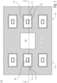
- FIG. 1 illustrates, in a simplified top-side-up plan view, an example semiconductor device 100 having a plurality of RF sub-assemblies at a stage of manufacture in accordance with an embodiment.
- the semiconductor device 100 includes a semiconductor die 102, a package substrate (not shown), and RF sub-assemblies 118 and 120 partially encapsulated with an encapsulant 104 (e.g., epoxy molding compound).
- an encapsulant 104 e.g., epoxy molding compound
- each of the RF sub-assemblies 118 and 120 include a conductive radiant element 106, 108 and surrounding conductive shield 110, 112 formed on a sacrificial blank (not shown).
- the term "conductive,” as used herein, generally refers to electrical conductivity unless otherwise specified.
- a patterned dielectric material 114, 116 formed on the sacrificial blank electrically isolates the respective conductive radiant elements 106, 108 from surrounding conductive shields 110, 112.
- the group of RF sub-assemblies 118 may be characterized as receiver (RX) sub-assemblies and the group of RF sub-assemblies 120 may be characterized as transmitter (TX) sub-assemblies.
- RX receiver
- TX transmitter
- the size and shape of the RF sub-assemblies 118 and 120 along with the number and arrangement of the RF sub-assemblies 118 and 120 in this embodiment are chosen for illustration purposes.
- the semiconductor device 100 may include any number of RF sub-assemblies 118 and 120, arranged accordingly. Simplified cross-sectional views of the example semiconductor device 100 taken along line A-A at stages of manufacture are depicted in FIG. 2 through FIG. 10 .
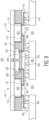
- FIG. 2 illustrates, in a simplified bottom-side-up cross-sectional view, the example semiconductor device 100 taken along line A-A at a stage of manufacture in accordance with an embodiment.
- the semiconductor device 100 includes the semiconductor die 102 and pre-formed RF sub-assemblies 118 and 120 placed on a carrier substrate 204.
- the carrier substrate 204 is configured and arranged to provide a temporary structure for placement of the semiconductor die 102 and the RF sub-assemblies 118 and 120 during encapsulation at a subsequent stage of manufacture, for example.
- the semiconductor die 102 has an active side (e.g., major side having circuitry) and a backside (e.g., major side opposite of the active side).
- the semiconductor die 102 includes bond pads 202 formed at the active side. Bond pads 202 may be configured for connection to respective conductive radiant elements 106 and 108 of the RF sub-assemblies 118 and 120 by way of a package substrate formed at a subsequent stage, for example.
- semiconductor die 102 is configured in an active-side-up orientation with the backside placed on the carrier substrate 204.
- the semiconductor die 102 may be formed from any suitable semiconductor material, such as silicon, germanium, gallium arsenide, gallium nitride, and the like.
- the semiconductor die 102 may further include any digital circuits, analog circuits, RF circuits, memory, processor, the like, and combinations thereof at the active side.
- conductive die connectors 208 have a first end affixed to respective bond pads 202.
- the conductive die connectors 208 may be in the form of any suitable conductive structures such as gold studs, copper pillars, solder balls, and the like.
- the conductive die connectors 208 may be formed or affixed at a subsequent stage of manufacture. For example, after an encapsulation operation, the bond pads 202 may be exposed (e.g., by way of an etch, laser ablation, or other suitable process) to form or affix the conductive die connectors.
- the RF sub-assemblies 118 and 120 are pre-formed before being placed on the carrier substrate 204.
- Each of the RF sub-assemblies 118 and 120 has a top side (e.g., major side having exposed surface of the sacrificial blank) and a backside (e.g., major side having the conductive radiant element).
- the RF sub-assemblies 118 and 120 are orientated with the top side placed on the carrier substrate 204.
- Each of the RF sub-assemblies 118 and 120 includes a sacrificial blank 206 having a conductive radiant element (106, 108) formed on a first major side and a surrounding conductive shield (110, 112) formed on outer sidewalls of the sacrificial blank.
- the patterned dielectric material 114 and 116 is formed on the first major side of the sacrificial blank and configured to electrically isolate the respective conductive radiant elements 106 and 108 from the surrounding conductive shields 110 and 112.
- a portion of the conductive shield (110, 112) may be extended onto the first major side and in a same plane as the respective conductive radiant element (106, 108).
- the sacrificial blank 206 may be formed from suitable materials such as non-crystalline glass, ceramic, quartz, plastic, polymer, and the like.
- the material composition of the sacrificial blank 206 is selected such that the sacrificial blank material may be etched by an etchant, melted, or dissolved without attacking an encapsulant, for example.
- the composition of the sacrificial blank 206 may be further chosen based on a desired coefficient of thermal expansion (CTE) property. For example, it may be desirable to choose a sacrificial blank 206 with a CTE property substantially similar to a CTE property of the encapsulant 104 to minimize package warpage.
- CTE coefficient of thermal expansion
- the sacrificial blank 206 may be formed in any desired shape and sidewall profile configured to form a desired cavity at a subsequent stage of manufacture. Simplified cross-sectional views of example RF sub-assemblies taken at stages of manufacture are depicted in FIG. 11 through FIG. 19 .
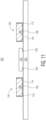
- FIG. 3 illustrates, in a simplified bottom-side-up cross-sectional view, the example semiconductor device 100 taken along line A-A at a subsequent stage of manufacture in accordance with an embodiment.
- the semiconductor device 100 includes the semiconductor die 102 and RF sub-assemblies 118 and 120 at least partially encapsulated with an encapsulant 302 while temporarily affixed on the carrier substrate 204.
- the encapsulated semiconductor device 100 has a first major side 304 formed on the carrier substrate 204 and a second major side 306 (opposite of the first major side 304).
- the encapsulant 302 as depicted in this cross-sectional view, corresponds to the encapsulant 104 depicted in the plan view of FIG. 1 .
- the semiconductor die 102 and RF sub-assemblies 118 and 120 are over-molded with the encapsulant 302 by way of a molding process.
- the encapsulated semiconductor device 100 is then subjected to a back grind operation to expose portions of the radiant elements 106 and 108, conductive shields 110 and 112, and conductive die connectors 208 at the second major side 306.
- the semiconductor die 102 and RF sub-assemblies 118 and 120 may be molded with the encapsulant 302 by way of a film-assisted molding (FAM) process.
- FAM film-assisted molding
- a FAM tool using a conformal film may be engaged with predetermined portions of the radiant elements 106 and 108, conductive shields 110 and 112, and conductive die connectors 208 during the molding process to keep the predetermined portions free from encapsulant.
- portions of the radiant elements 106 and 108, conductive shields 110 and 112, and conductive die connectors 208 may be exposed at the second major side 306 of the encapsulant 302 without a back grind operation.
- FIG. 4 illustrates, in a simplified bottom-side-up cross-sectional view, the example semiconductor device 100 taken along line A-A at a subsequent stage of manufacture in accordance with an embodiment.
- an interconnecting package substrate 414 is applied to the second major side 306 of the encapsulated semiconductor device 100.
- the package substrate 414 includes conductive features (e.g., traces 404-410) surrounded by non-conductive material 402 (e.g., dielectric).
- the package substrate 414 may be formed as a build-up substrate or may be provided as a pre-formed substrate.
- the conductive traces 404 and 406 are formed to interconnect the semiconductor die 102 and the radiant elements 106 and 108 and the conductive traces 408 and 410 are formed to interconnect the conductive shields 110 and 112 with a printed circuit board (PCB), for example.
- Openings 412 in the non-conductive material 402 expose portions of traces 408 and 410 configured for attachment of conductive connectors at a subsequent stage of manufacture.
- FIG. 5 illustrates, in a simplified cross-sectional view, the example semiconductor device 100 taken along line A-A at a subsequent stage of manufacture in accordance with an embodiment.
- the encapsulated semiconductor device 100 is separated from the carrier substrate 204 and reoriented (e.g., flipped).
- the backside of the semiconductor die 102 and a second major side (opposite of the first major side) of the sacrificial blanks 206 are exposed at the first major side 304 of encapsulated semiconductor device 100 when the carrier substrate 204 is removed.
- FIG. 6 illustrates, in a simplified cross-sectional view, the example semiconductor device 100 taken along line A-A at a subsequent stage of manufacture in accordance with an embodiment.
- the sacrificial blanks (206) are removed to form cavities 602 and 604 in respective RF sub-assemblies 118 and 120.
- the sacrificial blanks may be etched by an etchant, melted, or dissolved by way of suitable processes to form cavities 602 and 604.
- the composition of the sacrificial blanks allows for the sacrificial blank material to be etched by an etchant that does not etch or otherwise attack the encapsulant 302, radiant elements 106 and 108, and conductive shields 110 and 112, for example.
- the conductive shields 110 and 112 are configured for subsequent connection to a ground voltage supply by way of traces 408 and 410 of the package substrate 414, for example.
- FIG. 7A illustrates, in a simplified cross-sectional view, the example semiconductor device 100 taken along line A-A at a subsequent stage of manufacture in accordance with an embodiment.
- a pre-formed conductive package lid 702 is affixed on the first major side 304 of encapsulated semiconductor device 100 to enclose cavities 602 and 604.
- the package lid 702 is affixed on the first major side 304 of the encapsulated semiconductor device 100 by way of a conductive adhesive 704.
- the package lid may be formed from a suitable conductive material or a conductive metal coated material (e.g., metal coated laminate, metal coated plastic). With the package lid 702 attached, a continuous conductive resonant cavity is formed.
- the enclosed cavities 602 and 604 may be filled with air or other suitable low loss materials (e.g., gas, foam) having suitable dissipation factor (e.g., Df value in a range of 0 to 0.001) and dielectric constant (e.g., Dk value in a range of 1 to 3) properties.
- the package lid 702 portion over the cavities 602 and 604 is configured to serve as a signal reflector 708 to increase gain for propagation of RF signals such as 5G, 6G, and radar signals having frequencies of 20 GHz and higher.
- the signal reflector 708 portion of the package lid 702 over the cavities 602 and 604 is located at a predetermined distance 706 from radiant elements 106 and 108 for a desired resonant frequency and bandwidth.
- FIG. 7B illustrates, in a simplified cross-sectional view, the example semiconductor device 100 taken along line A-A at an alternative stage of manufacture in accordance with an embodiment.
- an alternative pre-formed conductive package lid 710 is affixed on the first major side 304 of encapsulated semiconductor device 100 to enclose cavities 602 and 604.
- the package lid 710 depicted in FIG. 7B may be characterized as an alternative to the package lid 702 depicted in FIG. 7A .
- the package lid 710 includes tunable recesses 714 which are vertically aligned with cavities 602 and 604.
- the recesses 714 may be tunable by forming the recesses to a desired depth during a stamping process.
- the signal reflector 716 portion of the recesses 714 over the cavities 602 and 604 is configured to provide an extended predetermined distance 712 from radiant elements 106 and 108 for increased gain and a desired resonant frequency and bandwidth.
- desired resonant frequencies and bandwidths can be realized without being limited to the depth of cavities 602 and 604.
- FIG. 8 illustrates, in a simplified cross-sectional view, the example semiconductor device 100 taken along line A-A at a subsequent stage of manufacture in accordance with an embodiment.
- conductive connectors 802 e.g., solder balls
- the conductive connectors 802 are configured and arranged to provide conductive connections between the semiconductor device 100 and a PCB, for example.
- the conductive shields 110 and 112 of the RF sub-assemblies 118 and 120 may be interconnected to a ground voltage supply by way of traces 408 and 410 and conductive connectors 802, for example.
- the conductive connectors 802 may be in the form of any suitable conductive structures such as solder balls, gold studs, copper pillars, and the like, to connect conductive features of the semiconductor device 100 with the PCB.
- the exposed portions of conductive traces 408 and 410 may be plated for subsequent connection with the PCB by way of solder paste attachment or other suitable conductive attachment processes (e.g., ACF, ACP).
- FIG. 9 illustrates, in a simplified cross-sectional view, the example semiconductor device 100 taken along line A-A at a subsequent stage of manufacture in accordance with an embodiment.
- the semiconductor device 100 is attached to an example PCB 902.
- the semiconductor device 100 is configured in a downward firing arrangement.
- the PCB 902 includes through openings 904 substantially vertically aligned with the cavity sidewalls of the RF sub-assemblies 118 and 120 to allow for propagation of RF signals through the PCB.
- the sidewalls of the openings 904 may be formed with a metal lining to reduce RF signal radiation from propagating laterally.
- the conductive connectors 802 attached at the bottom of the package substrate 414 are affixed to a top side of the PCB using known techniques and materials. Conductive (e.g., metal) features of the PCB are not shown for illustrative purposes.
- FIG. 10 illustrates, in a simplified cross-sectional view, the example semiconductor device 100 taken along line A-A at a subsequent stage of manufacture in accordance with an embodiment.
- a waveguide structure 1010 is aligned and attached to the PCB 902.
- the waveguide structure 1010 is attached to a bottom side of the PCB 902 by way of an adhesive 1008.
- the adhesive 1008 may be characterized as a conductive adhesive configured to minimize RF signal radiation from propagating laterally at the PCB 902 to waveguide structure 1010 interface.
- the waveguide structure 1010 includes waveguides 1004 formed in a waveguide body 1002.
- Waveguide antennas 1006 are located at the distal ends of the waveguides 1004.
- the waveguide structure 1010 may be characterized as an air cavity waveguide having slot antennas.
- the waveguide body 1002 may be formed from a metal, plastic, or laminate material with the waveguides 1004 formed as air cavities.
- the waveguides 1004 may be formed with a metal lining when the waveguide body 1002 is formed from a plastic or laminate material, for example.
- FIG. 11 through FIG. 13 illustrate, in simplified cross-sectional views, the example semiconductor device 100 taken along line A-A at alternative stages of manufacture in accordance with an embodiment.
- the stages of manufacture depicted in FIG. 11 through FIG. 13 are an alternative to the stages of manufacture of the example semiconductor device 100 depicted in FIG. 2 through FIG. 4 , with stages of manufacture depicted in FIG. 5 through FIG. 10 remaining substantially similar.
- FIG. 11 illustrates, in a simplified top-side-up cross-sectional view, the example semiconductor device 100 taken along line A-A at an alternative stage of manufacture in accordance with an embodiment.
- the semiconductor device 100 includes the semiconductor die 102 and pre-formed RF sub-assemblies 118 and 120 placed on a carrier substrate 204.
- the semiconductor die 102 is configured in an active-side-down orientation with the active side placed on the carrier substrate 204 and the RF sub-assemblies 118 and 120 are orientated with the backside placed on the carrier substrate 204.
- the conductive die connectors 208 depicted in FIG. 2 may be eliminated.
- FIG. 12 illustrates, in a simplified top-side-up cross-sectional view, the example semiconductor device 100 taken along line A-A at a subsequent stage of manufacture in accordance with an embodiment.
- the semiconductor device 100 includes the semiconductor die 102 and RF sub-assemblies 118 and 120 at least partially encapsulated with encapsulant 302 while temporarily affixed on the carrier substrate 204.
- the semiconductor die 102 and RF sub-assemblies 118 and 120 are over-molded with the encapsulant 302 by way of a molding process.
- the encapsulated semiconductor device 100 is then subjected to a back grind operation to expose the top sides of the RF sub-assemblies 118 and 120 and surface of the sacrificial blanks 206 at the first major side 304 the encapsulated semiconductor device 100.
- the semiconductor die 102 and RF sub-assemblies 118 and 120 may be molded with the encapsulant 302 by way of a FAM process.
- a FAM tool using a conformal film may be engaged with predetermined portions of the top side of the RF sub-assemblies 118 and 120 during the molding process to keep the predetermined portions free from encapsulant.
- the top sides of the RF sub-assemblies 118 and 120 and surface of the sacrificial blanks 206 may be exposed at the first major side 304 the encapsulated semiconductor device 100 without using a back grind operation.
- FIG. 13 illustrates, in a simplified bottom-side-up cross-sectional view, the example semiconductor device 100 taken along line A-A at a subsequent stage of manufacture in accordance with an embodiment.
- the interconnecting package substrate 414 is applied to the second major side 306 of the encapsulated semiconductor device 100.
- the encapsulated semiconductor device 100 is separated from the carrier substrate 204, reoriented (e.g., flipped) and placed onto a carrier substrate (e.g., carrier substrate 204 or other carrier substrate).
- a carrier substrate e.g., carrier substrate 204 or other carrier substrate.
- the package substrate 414 is applied to the second major side 306.
- the conductive traces 404 and 406 are formed to interconnect the semiconductor die 102 and the radiant elements 106 and 108 and the conductive traces 408 and 410 are formed to interconnect the conductive shields 110 and 112 with a PCB.
- the conductive shields 110 and 112 are configured for subsequent connection to a ground voltage supply by way of traces 408 and 410 of the package substrate 414.
- Openings 412 in the non-conductive material 402 expose portions of traces 408 and 410 configured for attachment of conductive connectors at a subsequent stage of manufacture (e.g., FIG. 8 ).
- the package substrate 414 may be formed as a build-up substrate or may be provided as a pre-formed substrate. After the package substrate 414 is applied to the second major side 306 of the encapsulated semiconductor device 100, subsequent stages of manufacture are depicted in FIG. 5 through FIG. 10 accordingly.
- FIG. 14 through FIG. 18 illustrate, in simplified cross-sectional views, an example RF sub-assembly at stages of manufacture in accordance with an embodiment.
- the RF sub-assembly depicted in FIG. 14 through FIG. 18 corresponds to the pre-formed RF sub-assemblies 118 and 120 of the semiconductor device 100, for example.
- FIG. 14 illustrates, in a simplified cross-sectional view, the example RF sub-assembly at a stage of manufacture in accordance with an embodiment.
- a bulk sacrificial blank 1402 is provided and a dielectric layer 1404 is formed on a first major side of the sacrificial blank.
- the sacrificial blank 1402 may be formed from suitable materials such as non-crystalline glass, ceramic, quartz, plastic, polymer, and the like.
- the material composition of the sacrificial blank 1402 is selected such that the sacrificial blank material may be subsequently removed by way of etching, melting, or dissolving, for example.
- the dielectric layer 1404 may be formed from suitable non-conductive materials such as Ajinomoto build-up film (ABF), for example.
- ABS Ajinomoto build-up film
- FIG. 15 illustrates, in a simplified cross-sectional view, the example RF sub-assembly at a subsequent stage of manufacture in accordance with an embodiment.
- the dielectric layer 1404 formed on the first major side of the sacrificial blank 1402 is patterned to form isolation structures 1502.
- the isolation structures 1502 are configured to electrically isolate conductive radiant elements and respective surrounding conductive shields formed at a subsequent stage.
- FIG. 16 illustrates, in a simplified cross-sectional view, the example RF sub-assembly at a subsequent stage of manufacture in accordance with an embodiment.
- the sacrificial blank 1402 is partially sawn to form singulation grooves 1602.
- the singulation grooves 1602 are formed by way of a mechanical saw process, for example.
- the singulation grooves 1602 are sawn to a significant depth of the bulk sacrificial blank 1402 such that individual RF sub-assemblies may be singulated at a subsequent stage.
- the singulation grooves 1602 may be formed by way of laser ablation, patterned plasma etching, or other suitable material removal process.
- FIG. 17 illustrates, in a simplified cross-sectional view, the example RF sub-assembly at a subsequent stage of manufacture in accordance with an embodiment.
- a conductive (e.g., metal) layer 1702 is formed on the sacrificial blank 1402.
- the upper surfaces of the sacrificial blank 1402 are selectively plated (e.g., isolation structures 1502 not plated) with a suitable metal or metal alloy (e.g., copper) material to form radiant element and conductive shield regions.
- the conductive layer 1702 and the isolation structures 1502 are substantially coplanar at the top surface of the sacrificial blank 1402.
- a seed layer (not shown) may be formed on the exposed upper surfaces of the sacrificial blank 1402 to facilitate a plating process, for example.
- other metallization techniques may be utilized to form the conductive layer 1702.
- FIG. 18 illustrates, in a simplified cross-sectional view, the example RF sub-assembly at a subsequent stage of manufacture in accordance with an embodiment.
- RF sub-assemblies are singulated.
- the back side of the sacrificial blank 1402 is subjected to a back grind operation to singulate the RF sub-assemblies 1810 and 1812.
- Each of the RF sub-assemblies 1810 and 1812 includes a sacrificial blank 1402, a radiant element (1802, 1804), and a surrounding conductive shield (1806, 1808).
- the patterned dielectric material 1502 is configured and arranged to electrically isolate the conductive radiant elements 1802 and 1804 from the respective conductive shields 1806 and 1808.
- the size, shape, and number of singulated RF sub-assemblies 1810 and 1812 are chosen for illustration purposes.
- FIG. 19 through FIG. 22 illustrate, in simplified cross-sectional views, an alternative example RF sub-assembly at stages of manufacture in accordance with an embodiment.
- the alternative RF sub-assembly depicted in FIG. 19 through FIG. 22 may be characterized as a multichannel RF sub-assembly having at least two RF sub-assembly portions share a common conductive isolation sidewall, for example.
- FIG. 19 illustrates, in a simplified cross-sectional view, the alternative RF sub-assembly at a stage of manufacture in accordance with an embodiment.
- a bulk sacrificial blank 1902 is provided and a dielectric layer is patterned to form isolation structures 1904 on a first major side of the sacrificial blank.
- the isolation structures 1904 are configured to electrically isolate conductive radiant elements and respective surrounding conductive shields formed at a subsequent stage, for example.
- the sacrificial blank 1902 may be formed from suitable materials such as non-crystalline glass, ceramic, quartz, plastic, polymer, and the like.
- the material composition of the sacrificial blank 1902 is selected such that the sacrificial blank material may be subsequently removed by way of etching, melting, or dissolving, for example.
- the isolation structures 1904 may be formed from suitable non-conductive materials such as ABF, for example.
- FIG. 20 illustrates, in a simplified cross-sectional view, the alternative RF sub-assembly at a subsequent stage of manufacture in accordance with an embodiment.
- the sacrificial blank 1902 is partially sawn to form singulation grooves 2002 and isolation groove 2004.
- the singulation grooves 2002 and isolation grooves 2004 are formed by way of a mechanical saw process, for example.
- the singulation grooves 2002 are sawn to a significant depth of the bulk sacrificial blank 1902 such that (e.g., multichannel) RF sub-assemblies may be singulated at a subsequent stage.
- the singulation grooves 2002 and isolation grooves 2004 may be formed by way of laser ablation, patterned plasma etching, or other suitable material removal process.
- FIG. 21 illustrates, in a simplified cross-sectional view, the alternative RF sub-assembly at a subsequent stage of manufacture in accordance with an embodiment.
- a conductive (e.g., metal) layer 2102 is formed on the sacrificial blank 1902.
- the upper surfaces of the sacrificial blank 1902 are selectively plated (e.g., isolation structures 1904 not plated) with a suitable metal or metal alloy (e.g., copper) material to form radiant element and conductive shield regions.
- the conductive layer 2102 and the isolation structures 1904 are substantially coplanar at the top surface of the sacrificial blank 1902.
- a seed layer (not shown) may be formed on the exposed upper surfaces of the sacrificial blank 1902 to facilitate a plating process, for example.
- FIG. 22 illustrates, in a simplified cross-sectional view, the alternative RF sub-assembly at a subsequent stage of manufacture in accordance with an embodiment.
- multichannel RF sub-assemblies 2208 are singulated.
- the back side of the sacrificial blank 1902 is subjected to a back grind operation to singulate the multichannel RF sub-assemblies 2208.
- each of the multichannel RF sub-assemblies 2208 includes a first RF sub-assembly portion 2210 and a second RF sub-assembly portion 2212 sharing a common conductive isolation sidewall 2214.
- Each of the RF sub-assembly portions 2210 and 212 includes a sacrificial blank 1902, a radiant element (2202, 2204), and a surrounding conductive shield 2206 with shared conductive isolation sidewall 2214.
- the patterned dielectric material 1904 is configured and arranged to electrically isolate the conductive radiant elements 2202 and 2204 from the conductive shield 2206.
- the size, shape, and number of multichannel RF sub-assembly portions 2210 and 2212 of the multichannel RF sub-assemblies 2208 are chosen for illustration purposes.
- a method of manufacturing a semiconductor device including placing a semiconductor die on a carrier substrate; placing a radio frequency (RF) sub-assembly on the carrier substrate, the RF sub-assembly comprising a sacrificial blank; a conductive radiant element formed on a first side of the sacrificial blank; and a conductive shield formed at least on outer sidewalls of the sacrificial blank; encapsulating with an encapsulant at least a portion of the semiconductor die and the RF sub-assembly; separating the carrier substrate from a first major side of the encapsulated semiconductor die and RF sub-assembly to expose a second side of the sacrificial blank; removing the sacrificial blank to form a cavity in the RF sub-assembly, the conductive radiant element and the conductive shield exposed through the cavity; and affixing a package lid on the first major side of the encapsulated semiconductor die and RF sub
- RF radio frequency
- the method may further include forming a package substrate on a second major side of the encapsulated semiconductor die and RF sub-assembly.
- the package substrate may include a conductive trace interconnecting a bond pad of the semiconductor die and the conductive radiant element.
- the method may further include affixing conductive connectors to a bottom side of the package substrate, the conductive connectors configured and arranged to provide conductive connections between the semiconductor device and a printed circuit board (PCB).
- the semiconductor device may be arranged in a downward firing configuration and configured for propagation of the RF signal through an opening in the PCB, the opening vertically aligned with the cavity.
- the cavity may be substantially filled with a low loss dielectric material.
- the conductive radiant element and the conductive shield may be formed by way of a same metallization process step.
- the package lid may be further configured to increase gain of the RF signal when transmitted or received by way of the conductive radiant element.
- the package lid may be affixed to the second major side of the encapsulated semiconductor die and RF sub-assembly by way of a conductive adhesive material.
- a method of manufacturing a semiconductor device including placing a semiconductor die on a carrier substrate; placing a radio frequency (RF) sub-assembly on the carrier substrate, the RF sub-assembly comprising a sacrificial blank; a patterned dielectric material formed on a first side of the sacrificial blank; a conductive radiant element formed on the first side of the sacrificial blank, the conductive radiant element formed in a same horizontal plane as the patterned dielectric material; and a conductive shield formed at least on outer sidewalls of the sacrificial blank; encapsulating with an encapsulant at least a portion of the semiconductor die and the RF sub-assembly; separating the carrier substrate from a first major side of the encapsulated semiconductor die and RF sub-assembly to expose a second side of the sacrificial blank; etching the sacrificial blank to form a cavity in the RF sub-assembl
- the conductive radiant element and the conductive shield may be formed by way of a same metallization process step.
- the method patterned dielectric material may be configured and arranged to electrically isolate the conductive radiant element from the conductive shield.
- the method of claim 10 wherein the package lid may be affixed to the second major side of the encapsulated semiconductor die and RF sub-assembly by way of a conductive adhesive material.
- the method may further include forming a package substrate on a second major side of the encapsulated semiconductor die and RF sub-assembly, the package substrate including a conductive trace interconnecting a bond pad of the semiconductor die and the conductive radiant element.
- the method may further include affixing conductive connectors to a bottom side of the package substrate, the conductive connectors configured and arranged to provide conductive connections between the semiconductor device and a printed circuit board (PCB) wherein the PCB includes a through opening vertically aligned with the cavity.
- PCB printed circuit board
- a method of manufacturing a semiconductor device including placing a semiconductor die on a carrier substrate; placing a radio frequency (RF) sub-assembly on the carrier substrate, the RF sub-assembly comprising a sacrificial blank; a patterned dielectric material formed on a first side of the sacrificial blank; a conductive radiant element formed on the first side of the sacrificial blank; and a conductive shield formed at least on outer sidewalls of the sacrificial blank, the patterned dielectric material configured to electrically isolate the conductive radiant element from the conductive shield; encapsulating with an encapsulant at least a portion of the semiconductor die and the RF sub-assembly; separating the carrier substrate from a first major side of the encapsulated semiconductor die and RF sub-assembly to expose a second side of the sacrificial blank; etching the sacrificial blank to form a cavity in the RF sub-a
- the package lid may be configured to serve as a signal reflector for propagation of an RF signal transmitted or received by way of the conductive radiant element.
- the portion of the package lid enclosing the cavity may be substantially parallel to a bottom surface of the cavity and spaced a predetermined distance from the conductive radiant element at the bottom surface of the cavity.
- the method may further include forming a package substrate on a second major side of the encapsulated semiconductor die and RF sub-assembly, the package substrate including a conductive trace interconnecting a bond pad of the semiconductor die and the conductive radiant element.
- the semiconductor device may be configured for propagation of the RF signal through an opening in an attached printed circuit board (PCB), the opening vertically aligned with the cavity.
- PCB printed circuit board
- the semiconductor device includes a semiconductor die and a pre-formed RF sub-assembly at least partially encapsulated with an encapsulant while on a carrier substrate.
- the RF sub-assembly includes a sacrificial blank having a conductive radiant element formed on a first major side and a surrounding conductive shield formed partially on the first major side and on outer sidewalls. After encapsulation, portions of the radiant element, conductive shield, and conductive die connectors are exposed.
- the semiconductor die is interconnected with the radiant element by way of a package substrate and associated die connectors.
- a second major side of the sacrificial blank is exposed.
- the sacrificial blank is subsequently removed to form a cavity having the radiant element and surrounding shield exposed in the cavity.
- a conductive lid is attached to enclose the cavity, thus forming a resonant RF cavity.
Landscapes
- Physics & Mathematics (AREA)
- Engineering & Computer Science (AREA)
- Electromagnetism (AREA)
- Manufacturing & Machinery (AREA)
- Microelectronics & Electronic Packaging (AREA)
- Shielding Devices Or Components To Electric Or Magnetic Fields (AREA)
- Geometry (AREA)
- Health & Medical Sciences (AREA)
- Toxicology (AREA)
Abstract
Description
- This disclosure relates generally to semiconductor device packaging, and more specifically, to semiconductor devices with an enclosed cavity and method of forming the same.
- Today, there is an increasing trend to include sophisticated semiconductor devices in products and systems that are used every day. These sophisticated semiconductor devices may include features for specific applications which may impact the configuration of the semiconductor device packages, for example. For some features and applications, the configuration of the semiconductor device packages may be susceptible to lower reliability, lower performance, and higher product or system costs. Accordingly, significant challenges exist in accommodating these features and applications while minimizing the impact on semiconductor devices' reliability, performance, and costs.
- The present invention is illustrated by way of example and is not limited by the accompanying figures, in which like references indicate similar elements. Elements in the figures are illustrated for simplicity and clarity and have not necessarily been drawn to scale.
-
FIG. 1 illustrates, in a simplified top-side-up plan view, an example semiconductor device having a plurality of enclosed radio frequency (RF) cavities at a stage of manufacture in accordance with an embodiment. -
FIG. 2 through FIG. 10 illustrate, in simplified cross-sectional views, the example semiconductor device at stages of manufacture in accordance with an embodiment. -
FIG. 11 through FIG. 13 illustrate, in simplified cross-sectional views, the example semiconductor device at alternative stages of manufacture in accordance with an embodiment. -
FIG. 14 through FIG. 18 illustrate, in simplified cross-sectional views, an example RF sub-assembly of the example semiconductor device at stages of manufacture in accordance with an embodiment. -
FIG. 19 through FIG. 22 illustrate, in simplified cross-sectional views, an alternative example RF sub-assembly of the example semiconductor device at stages of manufacture in accordance with an embodiment. - Generally, there is provided, a semiconductor device with an enclosed resonant RF cavity. The semiconductor device includes a semiconductor die and a pre-formed RF sub-assembly at least partially encapsulated with an encapsulant while on a carrier substrate. The RF sub-assembly includes a sacrificial blank having a conductive radiant element formed on a first major side and a surrounding conductive shield formed partially on the first major side and on outer sidewalls. After encapsulation, portions of the radiant element, conductive shield, and conductive die connectors are exposed. The semiconductor die is interconnected with the radiant element by way of a package substrate and associated die connectors. After the carrier substrate is removed, a second major side of the sacrificial blank is exposed. The sacrificial blank is subsequently removed to form a cavity having the radiant element and surrounding shield exposed in the cavity. A conductive lid is attached to enclose the cavity, thus forming a resonant RF cavity. By forming the semiconductor device with the enclosed resonant RF cavity in this manner, low loss RF signal propagation can be realized.
-
FIG. 1 illustrates, in a simplified top-side-up plan view, anexample semiconductor device 100 having a plurality of RF sub-assemblies at a stage of manufacture in accordance with an embodiment. At this stage of manufacture, thesemiconductor device 100 includes asemiconductor die 102, a package substrate (not shown), andRF sub-assemblies RF sub-assemblies radiant element conductive shield dielectric material radiant elements conductive shields RF sub-assemblies 118 may be characterized as receiver (RX) sub-assemblies and the group ofRF sub-assemblies 120 may be characterized as transmitter (TX) sub-assemblies. The size and shape of theRF sub-assemblies RF sub-assemblies semiconductor device 100 may include any number ofRF sub-assemblies example semiconductor device 100 taken along line A-A at stages of manufacture are depicted inFIG. 2 through FIG. 10 . -
FIG. 2 illustrates, in a simplified bottom-side-up cross-sectional view, theexample semiconductor device 100 taken along line A-A at a stage of manufacture in accordance with an embodiment. At this stage, thesemiconductor device 100 includes the semiconductor die 102 andpre-formed RF sub-assemblies carrier substrate 204. Thecarrier substrate 204 is configured and arranged to provide a temporary structure for placement of thesemiconductor die 102 and theRF sub-assemblies - The
semiconductor die 102 has an active side (e.g., major side having circuitry) and a backside (e.g., major side opposite of the active side). The semiconductor die 102 includesbond pads 202 formed at the active side.Bond pads 202 may be configured for connection to respective conductiveradiant elements RF sub-assemblies semiconductor die 102 is configured in an active-side-up orientation with the backside placed on thecarrier substrate 204. The semiconductor die 102 may be formed from any suitable semiconductor material, such as silicon, germanium, gallium arsenide, gallium nitride, and the like. The semiconductor die 102 may further include any digital circuits, analog circuits, RF circuits, memory, processor, the like, and combinations thereof at the active side. In this embodiment,conductive die connectors 208 have a first end affixed torespective bond pads 202. Theconductive die connectors 208 may be in the form of any suitable conductive structures such as gold studs, copper pillars, solder balls, and the like. Alternatively, theconductive die connectors 208 may be formed or affixed at a subsequent stage of manufacture. For example, after an encapsulation operation, thebond pads 202 may be exposed (e.g., by way of an etch, laser ablation, or other suitable process) to form or affix the conductive die connectors. - The
RF sub-assemblies carrier substrate 204. Each of theRF sub-assemblies RF sub-assemblies carrier substrate 204. Each of theRF sub-assemblies dielectric material radiant elements conductive shields - The sacrificial blank 206 may be formed from suitable materials such as non-crystalline glass, ceramic, quartz, plastic, polymer, and the like. The material composition of the sacrificial blank 206 is selected such that the sacrificial blank material may be etched by an etchant, melted, or dissolved without attacking an encapsulant, for example. The composition of the
sacrificial blank 206 may be further chosen based on a desired coefficient of thermal expansion (CTE) property. For example, it may be desirable to choose a sacrificial blank 206 with a CTE property substantially similar to a CTE property of the encapsulant 104 to minimize package warpage. The sacrificial blank 206 may be formed in any desired shape and sidewall profile configured to form a desired cavity at a subsequent stage of manufacture. Simplified cross-sectional views of example RF sub-assemblies taken at stages of manufacture are depicted inFIG. 11 through FIG. 19 . -
FIG. 3 illustrates, in a simplified bottom-side-up cross-sectional view, theexample semiconductor device 100 taken along line A-A at a subsequent stage of manufacture in accordance with an embodiment. At this stage, thesemiconductor device 100 includes thesemiconductor die 102 andRF sub-assemblies encapsulant 302 while temporarily affixed on thecarrier substrate 204. For illustration purposes, theencapsulated semiconductor device 100 has a firstmajor side 304 formed on thecarrier substrate 204 and a second major side 306 (opposite of the first major side 304). Theencapsulant 302, as depicted in this cross-sectional view, corresponds to the encapsulant 104 depicted in the plan view ofFIG. 1 . - In this embodiment, the semiconductor die 102 and
RF sub-assemblies encapsulant 302 by way of a molding process. The encapsulatedsemiconductor device 100 is then subjected to a back grind operation to expose portions of theradiant elements conductive shields conductive die connectors 208 at the secondmajor side 306. Alternatively, the semiconductor die 102 andRF sub-assemblies encapsulant 302 by way of a film-assisted molding (FAM) process. For example, a FAM tool using a conformal film may be engaged with predetermined portions of theradiant elements conductive shields conductive die connectors 208 during the molding process to keep the predetermined portions free from encapsulant. In this manner, portions of theradiant elements conductive shields conductive die connectors 208 may be exposed at the secondmajor side 306 of theencapsulant 302 without a back grind operation. -
FIG. 4 illustrates, in a simplified bottom-side-up cross-sectional view, theexample semiconductor device 100 taken along line A-A at a subsequent stage of manufacture in accordance with an embodiment. At this stage, an interconnectingpackage substrate 414 is applied to the secondmajor side 306 of the encapsulatedsemiconductor device 100. After portions of theradiant elements conductive shields conductive die connectors 208 are exposed at the secondmajor side 306, thepackage substrate 414 is applied. Thepackage substrate 414 includes conductive features (e.g., traces 404-410) surrounded by non-conductive material 402 (e.g., dielectric). Thepackage substrate 414 may be formed as a build-up substrate or may be provided as a pre-formed substrate. - In this embodiment, the
conductive traces radiant elements conductive traces conductive shields Openings 412 in thenon-conductive material 402 expose portions oftraces -
FIG. 5 illustrates, in a simplified cross-sectional view, theexample semiconductor device 100 taken along line A-A at a subsequent stage of manufacture in accordance with an embodiment. At this stage, the encapsulatedsemiconductor device 100 is separated from thecarrier substrate 204 and reoriented (e.g., flipped). The backside of the semiconductor die 102 and a second major side (opposite of the first major side) of thesacrificial blanks 206 are exposed at the firstmajor side 304 of encapsulatedsemiconductor device 100 when thecarrier substrate 204 is removed. -
FIG. 6 illustrates, in a simplified cross-sectional view, theexample semiconductor device 100 taken along line A-A at a subsequent stage of manufacture in accordance with an embodiment. At this stage, the sacrificial blanks (206) are removed to formcavities respective RF sub-assemblies cavities encapsulant 302,radiant elements conductive shields radiant elements conductive shields dielectric material respective cavities conductive shields traces package substrate 414, for example. -
FIG. 7A illustrates, in a simplified cross-sectional view, theexample semiconductor device 100 taken along line A-A at a subsequent stage of manufacture in accordance with an embodiment. At this stage, a pre-formedconductive package lid 702 is affixed on the firstmajor side 304 of encapsulatedsemiconductor device 100 to enclosecavities package lid 702 is affixed on the firstmajor side 304 of the encapsulatedsemiconductor device 100 by way of aconductive adhesive 704. The package lid may be formed from a suitable conductive material or a conductive metal coated material (e.g., metal coated laminate, metal coated plastic). With thepackage lid 702 attached, a continuous conductive resonant cavity is formed. Theenclosed cavities package lid 702 portion over thecavities signal reflector 708 to increase gain for propagation of RF signals such as 5G, 6G, and radar signals having frequencies of 20 GHz and higher. Thesignal reflector 708 portion of thepackage lid 702 over thecavities predetermined distance 706 fromradiant elements -
FIG. 7B illustrates, in a simplified cross-sectional view, theexample semiconductor device 100 taken along line A-A at an alternative stage of manufacture in accordance with an embodiment. At this stage, an alternative pre-formedconductive package lid 710 is affixed on the firstmajor side 304 of encapsulatedsemiconductor device 100 to enclosecavities package lid 710 depicted inFIG. 7B may be characterized as an alternative to thepackage lid 702 depicted inFIG. 7A . In this embodiment, thepackage lid 710 includestunable recesses 714 which are vertically aligned withcavities package lid 710 formed from a metal material, therecesses 714 may be tunable by forming the recesses to a desired depth during a stamping process. Thesignal reflector 716 portion of therecesses 714 over thecavities predetermined distance 712 fromradiant elements recesses 714 in the package lid, desired resonant frequencies and bandwidths can be realized without being limited to the depth ofcavities -
FIG. 8 illustrates, in a simplified cross-sectional view, theexample semiconductor device 100 taken along line A-A at a subsequent stage of manufacture in accordance with an embodiment. At this stage, conductive connectors 802 (e.g., solder balls) are affixed to a bottom side of thepackage substrate 414. Theconductive connectors 802 are configured and arranged to provide conductive connections between thesemiconductor device 100 and a PCB, for example. Theconductive shields RF sub-assemblies traces conductive connectors 802, for example. Theconductive connectors 802 may be in the form of any suitable conductive structures such as solder balls, gold studs, copper pillars, and the like, to connect conductive features of thesemiconductor device 100 with the PCB. As an alternative to attachingconductive connectors 802, the exposed portions ofconductive traces 408 and 410 (e.g.,FIG. 7A ) may be plated for subsequent connection with the PCB by way of solder paste attachment or other suitable conductive attachment processes (e.g., ACF, ACP). -
FIG. 9 illustrates, in a simplified cross-sectional view, theexample semiconductor device 100 taken along line A-A at a subsequent stage of manufacture in accordance with an embodiment. At this stage, thesemiconductor device 100 is attached to anexample PCB 902. In this embodiment, thesemiconductor device 100 is configured in a downward firing arrangement. ThePCB 902 includes throughopenings 904 substantially vertically aligned with the cavity sidewalls of theRF sub-assemblies openings 904 may be formed with a metal lining to reduce RF signal radiation from propagating laterally. In this embodiment, theconductive connectors 802 attached at the bottom of thepackage substrate 414 are affixed to a top side of the PCB using known techniques and materials. Conductive (e.g., metal) features of the PCB are not shown for illustrative purposes. -
FIG. 10 illustrates, in a simplified cross-sectional view, theexample semiconductor device 100 taken along line A-A at a subsequent stage of manufacture in accordance with an embodiment. At this stage, awaveguide structure 1010 is aligned and attached to thePCB 902. In this embodiment, thewaveguide structure 1010 is attached to a bottom side of thePCB 902 by way of an adhesive 1008. In some embodiments, the adhesive 1008 may be characterized as a conductive adhesive configured to minimize RF signal radiation from propagating laterally at thePCB 902 towaveguide structure 1010 interface. - In this embodiment, the
waveguide structure 1010 includeswaveguides 1004 formed in awaveguide body 1002.Waveguide antennas 1006 are located at the distal ends of thewaveguides 1004. In this embodiment, thewaveguide structure 1010 may be characterized as an air cavity waveguide having slot antennas. For example, thewaveguide body 1002 may be formed from a metal, plastic, or laminate material with thewaveguides 1004 formed as air cavities. Thewaveguides 1004 may be formed with a metal lining when thewaveguide body 1002 is formed from a plastic or laminate material, for example. -
FIG. 11 through FIG. 13 illustrate, in simplified cross-sectional views, theexample semiconductor device 100 taken along line A-A at alternative stages of manufacture in accordance with an embodiment. The stages of manufacture depicted inFIG. 11 through FIG. 13 are an alternative to the stages of manufacture of theexample semiconductor device 100 depicted inFIG. 2 through FIG. 4 , with stages of manufacture depicted inFIG. 5 through FIG. 10 remaining substantially similar. -
FIG. 11 illustrates, in a simplified top-side-up cross-sectional view, theexample semiconductor device 100 taken along line A-A at an alternative stage of manufacture in accordance with an embodiment. At this stage, thesemiconductor device 100 includes the semiconductor die 102 andpre-formed RF sub-assemblies carrier substrate 204. In this embodiment, the semiconductor die 102 is configured in an active-side-down orientation with the active side placed on thecarrier substrate 204 and theRF sub-assemblies carrier substrate 204. By arranging the semiconductor die 102 and theRF sub-assemblies carrier substrate 204, theconductive die connectors 208 depicted inFIG. 2 may be eliminated. -
FIG. 12 illustrates, in a simplified top-side-up cross-sectional view, theexample semiconductor device 100 taken along line A-A at a subsequent stage of manufacture in accordance with an embodiment. At this stage, thesemiconductor device 100 includes the semiconductor die 102 andRF sub-assemblies encapsulant 302 while temporarily affixed on thecarrier substrate 204. In this embodiment, the semiconductor die 102 andRF sub-assemblies encapsulant 302 by way of a molding process. The encapsulatedsemiconductor device 100 is then subjected to a back grind operation to expose the top sides of theRF sub-assemblies sacrificial blanks 206 at the firstmajor side 304 the encapsulatedsemiconductor device 100. Alternatively, the semiconductor die 102 andRF sub-assemblies encapsulant 302 by way of a FAM process. For example, a FAM tool using a conformal film may be engaged with predetermined portions of the top side of theRF sub-assemblies RF sub-assemblies sacrificial blanks 206 may be exposed at the firstmajor side 304 the encapsulatedsemiconductor device 100 without using a back grind operation. -
FIG. 13 illustrates, in a simplified bottom-side-up cross-sectional view, theexample semiconductor device 100 taken along line A-A at a subsequent stage of manufacture in accordance with an embodiment. At this stage, the interconnectingpackage substrate 414 is applied to the secondmajor side 306 of the encapsulatedsemiconductor device 100. In this embodiment, the encapsulatedsemiconductor device 100 is separated from thecarrier substrate 204, reoriented (e.g., flipped) and placed onto a carrier substrate (e.g.,carrier substrate 204 or other carrier substrate). After the encapsulatedsemiconductor device 100 is separated from thecarrier substrate 204, portions of theradiant elements conductive shields bond pads 202 are exposed at the secondmajor side 306. - Similar to the embodiment of
FIG. 4 described above, thepackage substrate 414 is applied to the secondmajor side 306. The conductive traces 404 and 406 are formed to interconnect the semiconductor die 102 and theradiant elements conductive traces conductive shields conductive shields traces package substrate 414.Openings 412 in thenon-conductive material 402 expose portions oftraces FIG. 8 ). Thepackage substrate 414 may be formed as a build-up substrate or may be provided as a pre-formed substrate. After thepackage substrate 414 is applied to the secondmajor side 306 of the encapsulatedsemiconductor device 100, subsequent stages of manufacture are depicted inFIG. 5 through FIG. 10 accordingly. -
FIG. 14 through FIG. 18 illustrate, in simplified cross-sectional views, an example RF sub-assembly at stages of manufacture in accordance with an embodiment. The RF sub-assembly depicted inFIG. 14 through FIG. 18 corresponds to thepre-formed RF sub-assemblies semiconductor device 100, for example. -
FIG. 14 illustrates, in a simplified cross-sectional view, the example RF sub-assembly at a stage of manufacture in accordance with an embodiment. At this stage, a bulk sacrificial blank 1402 is provided and adielectric layer 1404 is formed on a first major side of the sacrificial blank. The sacrificial blank 1402 may be formed from suitable materials such as non-crystalline glass, ceramic, quartz, plastic, polymer, and the like. The material composition of the sacrificial blank 1402 is selected such that the sacrificial blank material may be subsequently removed by way of etching, melting, or dissolving, for example. Thedielectric layer 1404 may be formed from suitable non-conductive materials such as Ajinomoto build-up film (ABF), for example. -
FIG. 15 illustrates, in a simplified cross-sectional view, the example RF sub-assembly at a subsequent stage of manufacture in accordance with an embodiment. At this stage, thedielectric layer 1404 formed on the first major side of the sacrificial blank 1402 is patterned to formisolation structures 1502. Theisolation structures 1502 are configured to electrically isolate conductive radiant elements and respective surrounding conductive shields formed at a subsequent stage. -
FIG. 16 illustrates, in a simplified cross-sectional view, the example RF sub-assembly at a subsequent stage of manufacture in accordance with an embodiment. At this stage, the sacrificial blank 1402 is partially sawn to formsingulation grooves 1602. In this embodiment, thesingulation grooves 1602 are formed by way of a mechanical saw process, for example. Thesingulation grooves 1602 are sawn to a significant depth of the bulk sacrificial blank 1402 such that individual RF sub-assemblies may be singulated at a subsequent stage. In some embodiments, thesingulation grooves 1602 may be formed by way of laser ablation, patterned plasma etching, or other suitable material removal process. -
FIG. 17 illustrates, in a simplified cross-sectional view, the example RF sub-assembly at a subsequent stage of manufacture in accordance with an embodiment. At this stage, a conductive (e.g., metal)layer 1702 is formed on the sacrificial blank 1402. In this embodiment, the upper surfaces of the sacrificial blank 1402 are selectively plated (e.g.,isolation structures 1502 not plated) with a suitable metal or metal alloy (e.g., copper) material to form radiant element and conductive shield regions. In this embodiment, theconductive layer 1702 and theisolation structures 1502 are substantially coplanar at the top surface of the sacrificial blank 1402. A seed layer (not shown) may be formed on the exposed upper surfaces of the sacrificial blank 1402 to facilitate a plating process, for example. In other embodiments, other metallization techniques may be utilized to form theconductive layer 1702. -
FIG. 18 illustrates, in a simplified cross-sectional view, the example RF sub-assembly at a subsequent stage of manufacture in accordance with an embodiment. At this stage, RF sub-assemblies are singulated. In this embodiment, the back side of the sacrificial blank 1402 is subjected to a back grind operation to singulate theRF sub-assemblies RF sub-assemblies dielectric material 1502 is configured and arranged to electrically isolate the conductiveradiant elements conductive shields singulated RF sub-assemblies -
FIG. 19 through FIG. 22 illustrate, in simplified cross-sectional views, an alternative example RF sub-assembly at stages of manufacture in accordance with an embodiment. The alternative RF sub-assembly depicted inFIG. 19 through FIG. 22 may be characterized as a multichannel RF sub-assembly having at least two RF sub-assembly portions share a common conductive isolation sidewall, for example. -
FIG. 19 illustrates, in a simplified cross-sectional view, the alternative RF sub-assembly at a stage of manufacture in accordance with an embodiment. At this stage, a bulk sacrificial blank 1902 is provided and a dielectric layer is patterned to formisolation structures 1904 on a first major side of the sacrificial blank. Theisolation structures 1904 are configured to electrically isolate conductive radiant elements and respective surrounding conductive shields formed at a subsequent stage, for example. The sacrificial blank 1902 may be formed from suitable materials such as non-crystalline glass, ceramic, quartz, plastic, polymer, and the like. The material composition of the sacrificial blank 1902 is selected such that the sacrificial blank material may be subsequently removed by way of etching, melting, or dissolving, for example. Theisolation structures 1904 may be formed from suitable non-conductive materials such as ABF, for example. -
FIG. 20 illustrates, in a simplified cross-sectional view, the alternative RF sub-assembly at a subsequent stage of manufacture in accordance with an embodiment. At this stage, the sacrificial blank 1902 is partially sawn to formsingulation grooves 2002 andisolation groove 2004. In this embodiment, thesingulation grooves 2002 andisolation grooves 2004 are formed by way of a mechanical saw process, for example. Thesingulation grooves 2002 are sawn to a significant depth of the bulk sacrificial blank 1902 such that (e.g., multichannel) RF sub-assemblies may be singulated at a subsequent stage. In some embodiments, thesingulation grooves 2002 andisolation grooves 2004 may be formed by way of laser ablation, patterned plasma etching, or other suitable material removal process. -
FIG. 21 illustrates, in a simplified cross-sectional view, the alternative RF sub-assembly at a subsequent stage of manufacture in accordance with an embodiment. At this stage, a conductive (e.g., metal)layer 2102 is formed on the sacrificial blank 1902. In this embodiment, the upper surfaces of the sacrificial blank 1902 are selectively plated (e.g.,isolation structures 1904 not plated) with a suitable metal or metal alloy (e.g., copper) material to form radiant element and conductive shield regions. In this embodiment, theconductive layer 2102 and theisolation structures 1904 are substantially coplanar at the top surface of the sacrificial blank 1902. A seed layer (not shown) may be formed on the exposed upper surfaces of the sacrificial blank 1902 to facilitate a plating process, for example. -
FIG. 22 illustrates, in a simplified cross-sectional view, the alternative RF sub-assembly at a subsequent stage of manufacture in accordance with an embodiment. At this stage,multichannel RF sub-assemblies 2208 are singulated. In this embodiment, the back side of the sacrificial blank 1902 is subjected to a back grind operation to singulate themultichannel RF sub-assemblies 2208. In this embodiment, each of themultichannel RF sub-assemblies 2208 includes a firstRF sub-assembly portion 2210 and a secondRF sub-assembly portion 2212 sharing a commonconductive isolation sidewall 2214. Each of theRF sub-assembly portions 2210 and 212 includes a sacrificial blank 1902, a radiant element (2202, 2204), and a surroundingconductive shield 2206 with sharedconductive isolation sidewall 2214. The patterneddielectric material 1904 is configured and arranged to electrically isolate the conductiveradiant elements conductive shield 2206. The size, shape, and number of multichannelRF sub-assembly portions multichannel RF sub-assemblies 2208 and are chosen for illustration purposes. - Generally, there is provided, a method of manufacturing a semiconductor device including placing a semiconductor die on a carrier substrate; placing a radio frequency (RF) sub-assembly on the carrier substrate, the RF sub-assembly comprising a sacrificial blank; a conductive radiant element formed on a first side of the sacrificial blank; and a conductive shield formed at least on outer sidewalls of the sacrificial blank; encapsulating with an encapsulant at least a portion of the semiconductor die and the RF sub-assembly; separating the carrier substrate from a first major side of the encapsulated semiconductor die and RF sub-assembly to expose a second side of the sacrificial blank; removing the sacrificial blank to form a cavity in the RF sub-assembly, the conductive radiant element and the conductive shield exposed through the cavity; and affixing a package lid on the first major side of the encapsulated semiconductor die and RF sub-assembly, the package lid configured to serve as a signal reflector for propagation of an RF signal. The method may further include forming a package substrate on a second major side of the encapsulated semiconductor die and RF sub-assembly. The package substrate may include a conductive trace interconnecting a bond pad of the semiconductor die and the conductive radiant element. The method may further include affixing conductive connectors to a bottom side of the package substrate, the conductive connectors configured and arranged to provide conductive connections between the semiconductor device and a printed circuit board (PCB). The semiconductor device may be arranged in a downward firing configuration and configured for propagation of the RF signal through an opening in the PCB, the opening vertically aligned with the cavity. The cavity may be substantially filled with a low loss dielectric material. The conductive radiant element and the conductive shield may be formed by way of a same metallization process step. The package lid may be further configured to increase gain of the RF signal when transmitted or received by way of the conductive radiant element. The package lid may be affixed to the second major side of the encapsulated semiconductor die and RF sub-assembly by way of a conductive adhesive material.
- In another embodiment, there is provided, a method of manufacturing a semiconductor device including placing a semiconductor die on a carrier substrate; placing a radio frequency (RF) sub-assembly on the carrier substrate, the RF sub-assembly comprising a sacrificial blank; a patterned dielectric material formed on a first side of the sacrificial blank; a conductive radiant element formed on the first side of the sacrificial blank, the conductive radiant element formed in a same horizontal plane as the patterned dielectric material; and a conductive shield formed at least on outer sidewalls of the sacrificial blank; encapsulating with an encapsulant at least a portion of the semiconductor die and the RF sub-assembly; separating the carrier substrate from a first major side of the encapsulated semiconductor die and RF sub-assembly to expose a second side of the sacrificial blank; etching the sacrificial blank to form a cavity in the RF sub-assembly, the conductive radiant element and the conductive shield exposed through the cavity; and affixing a package lid on the first major side of the encapsulated semiconductor die and RF sub-assembly, the package lid configured to serve as a signal reflector for propagation of an RF signal. The conductive radiant element and the conductive shield may be formed by way of a same metallization process step. The method patterned dielectric material may be configured and arranged to electrically isolate the conductive radiant element from the conductive shield. The method of claim 10, wherein the package lid may be affixed to the second major side of the encapsulated semiconductor die and RF sub-assembly by way of a conductive adhesive material. The method may further include forming a package substrate on a second major side of the encapsulated semiconductor die and RF sub-assembly, the package substrate including a conductive trace interconnecting a bond pad of the semiconductor die and the conductive radiant element. The method may further include affixing conductive connectors to a bottom side of the package substrate, the conductive connectors configured and arranged to provide conductive connections between the semiconductor device and a printed circuit board (PCB) wherein the PCB includes a through opening vertically aligned with the cavity.
- In yet another embodiment, there is provided, a method of manufacturing a semiconductor device including placing a semiconductor die on a carrier substrate; placing a radio frequency (RF) sub-assembly on the carrier substrate, the RF sub-assembly comprising a sacrificial blank; a patterned dielectric material formed on a first side of the sacrificial blank; a conductive radiant element formed on the first side of the sacrificial blank; and a conductive shield formed at least on outer sidewalls of the sacrificial blank, the patterned dielectric material configured to electrically isolate the conductive radiant element from the conductive shield; encapsulating with an encapsulant at least a portion of the semiconductor die and the RF sub-assembly; separating the carrier substrate from a first major side of the encapsulated semiconductor die and RF sub-assembly to expose a second side of the sacrificial blank; etching the sacrificial blank to form a cavity in the RF sub-assembly, the conductive radiant element and the conductive shield exposed through the cavity; and affixing a package lid on the first major side of the encapsulated semiconductor die and RF sub-assembly, the package lid enclosing the cavity. The package lid may be configured to serve as a signal reflector for propagation of an RF signal transmitted or received by way of the conductive radiant element. The portion of the package lid enclosing the cavity may be substantially parallel to a bottom surface of the cavity and spaced a predetermined distance from the conductive radiant element at the bottom surface of the cavity. The method may further include forming a package substrate on a second major side of the encapsulated semiconductor die and RF sub-assembly, the package substrate including a conductive trace interconnecting a bond pad of the semiconductor die and the conductive radiant element. The semiconductor device may be configured for propagation of the RF signal through an opening in an attached printed circuit board (PCB), the opening vertically aligned with the cavity.
- By now, it should be appreciated that there has been provided a semiconductor device with an enclosed resonant RF cavity. The semiconductor device includes a semiconductor die and a pre-formed RF sub-assembly at least partially encapsulated with an encapsulant while on a carrier substrate. The RF sub-assembly includes a sacrificial blank having a conductive radiant element formed on a first major side and a surrounding conductive shield formed partially on the first major side and on outer sidewalls. After encapsulation, portions of the radiant element, conductive shield, and conductive die connectors are exposed. The semiconductor die is interconnected with the radiant element by way of a package substrate and associated die connectors. After the carrier substrate is removed, a second major side of the sacrificial blank is exposed. The sacrificial blank is subsequently removed to form a cavity having the radiant element and surrounding shield exposed in the cavity. A conductive lid is attached to enclose the cavity, thus forming a resonant RF cavity. By forming the semiconductor device with the enclosed resonant RF cavity in this manner, low loss RF signal propagation can be realized.
- The terms "front," "back," "top," "bottom," "over," "under" and the like in the description and in the claims, if any, are used for descriptive purposes and not necessarily for describing permanent relative positions. It is understood that the terms so used are interchangeable under appropriate circumstances such that the embodiments of the invention described herein are, for example, capable of operation in other orientations than those illustrated or otherwise described herein.
- Although the invention is described herein with reference to specific embodiments, various modifications and changes can be made without departing from the scope of the present invention as set forth in the claims below. Accordingly, the specification and figures are to be regarded in an illustrative rather than a restrictive sense, and all such modifications are intended to be included within the scope of the present invention. Any benefits, advantages, or solutions to problems that are described herein with regard to specific embodiments are not intended to be construed as a critical, required, or essential feature or element of any or all the claims.
- Furthermore, the terms "a" or "an," as used herein, are defined as one or more than one. Also, the use of introductory phrases such as "at least one" and "one or more" in the claims should not be construed to imply that the introduction of another claim element by the indefinite articles "a" or "an" limits any particular claim containing such introduced claim element to inventions containing only one such element, even when the same claim includes the introductory phrases "one or more" or "at least one" and indefinite articles such as "a" or "an." The same holds true for the use of definite articles.
- Unless stated otherwise, terms such as "first" and "second" are used to arbitrarily distinguish between the elements such terms describe. Thus, these terms are not necessarily intended to indicate temporal or other prioritization of such elements.
Claims (15)
- A method of manufacturing a semiconductor device, the method comprising:placing a semiconductor die on a carrier substrate;placing a radio frequency, RF, sub-assembly on the carrier substrate, the RF sub-assembly comprising:a sacrificial blank;a conductive radiant element formed on a first side of the sacrificial blank; anda conductive shield formed at least on outer sidewalls of the sacrificial blank;encapsulating with an encapsulant at least a portion of the semiconductor die and the RF sub-assembly;separating the carrier substrate from a first major side of the encapsulated semiconductor die and RF sub-assembly to expose a second side of the sacrificial blank;removing the sacrificial blank to form a cavity in the RF sub-assembly, the conductive radiant element and the conductive shield exposed through the cavity; andaffixing a package lid on the first major side of the encapsulated semiconductor die and RF sub-assembly, the package lid configured to serve as a signal reflector for propagation of an RF signal.
- The method of claim 1, further comprising forming a package substrate on a second major side of the encapsulated semiconductor die and RF sub-assembly.
- The method of claim 2, wherein the package substrate includes a conductive trace interconnecting a bond pad of the semiconductor die and the conductive radiant element.
- The method of claim 2 or 3, further comprising affixing conductive connectors to a bottom side of the package substrate, the conductive connectors configured and arranged to provide conductive connections between the semiconductor device and a printed circuit board (PCB).
- The method of claim 4, wherein the semiconductor device is arranged in a downward firing configuration and configured for propagation of the RF signal through an opening in the PCB, the opening vertically aligned with the cavity.
- The method of any preceding claim, wherein the cavity is substantially filled with a low loss dielectric material.
- The method of any preceding claim, wherein the conductive radiant element and the conductive shield are formed by way of a same metallization process step.
- The method of any preceding claim, wherein the package lid is further configured to increase gain of the RF signal when transmitted or received by way of the conductive radiant element.
- The method of any preceding claim, wherein the package lid is affixed to the second major side of the encapsulated semiconductor die and RF sub-assembly by way of a conductive adhesive material.
- A method of manufacturing a semiconductor device, the method comprising:placing a semiconductor die on a carrier substrate;placing a radio frequency, RF, sub-assembly on the carrier substrate, the RF sub-assembly comprising:a sacrificial blank;a patterned dielectric material formed on a first side of the sacrificial blank;a conductive radiant element formed on the first side of the sacrificial blank, the conductive radiant element formed in a same horizontal plane as the patterned dielectric material; anda conductive shield formed at least on outer sidewalls of the sacrificial blank;encapsulating with an encapsulant at least a portion of the semiconductor die and the RF sub-assembly;separating the carrier substrate from a first major side of the encapsulated semiconductor die and RF sub-assembly to expose a second side of the sacrificial blank;etching the sacrificial blank to form a cavity in the RF sub-assembly, the conductive radiant element and the conductive shield exposed through the cavity; andaffixing a package lid on the first major side of the encapsulated semiconductor die and RF sub-assembly, the package lid configured to serve as a signal reflector for propagation of an RF signal.
- The method of claim 10, wherein the conductive radiant element and the conductive shield are formed by way of a same metallization process step.
- The method of claim 10 or 11, wherein the patterned dielectric material is configured and arranged to electrically isolate the conductive radiant element from the conductive shield.
- The method of any of claims 10 to 12, wherein the package lid is affixed to the second major side of the encapsulated semiconductor die and RF sub-assembly by way of a conductive adhesive material.
- The method of any of claim 10 to 13, further comprising forming a package substrate on a second major side of the encapsulated semiconductor die and RF sub-assembly, the package substrate including a conductive trace interconnecting a bond pad of the semiconductor die and the conductive radiant element.
- The method of claim 14, further comprising affixing conductive connectors to a bottom side of the package substrate, the conductive connectors configured and arranged to provide conductive connections between the semiconductor device and a printed circuit board (PCB) wherein the PCB includes a through opening vertically aligned with the cavity.
Applications Claiming Priority (1)
| Application Number | Priority Date | Filing Date | Title |
|---|---|---|---|
| US17/805,955 US12381164B2 (en) | 2022-06-08 | 2022-06-08 | Semiconductor device with enclosed cavity and method therefor |
Publications (1)
| Publication Number | Publication Date |
|---|---|
| EP4290562A1 true EP4290562A1 (en) | 2023-12-13 |
Family
ID=86646603
Family Applications (1)
| Application Number | Title | Priority Date | Filing Date |
|---|---|---|---|
| EP23176430.9A Pending EP4290562A1 (en) | 2022-06-08 | 2023-05-31 | Method of fabricating an rf semiconductor device with an enclosed cavity |
Country Status (2)
| Country | Link |
|---|---|
| US (1) | US12381164B2 (en) |
| EP (1) | EP4290562A1 (en) |
Families Citing this family (1)
| Publication number | Priority date | Publication date | Assignee | Title |
|---|---|---|---|---|
| US12381164B2 (en) * | 2022-06-08 | 2025-08-05 | Nxp Usa, Inc. | Semiconductor device with enclosed cavity and method therefor |
Citations (5)
| Publication number | Priority date | Publication date | Assignee | Title |
|---|---|---|---|---|
| US20070026567A1 (en) * | 2005-06-01 | 2007-02-01 | Gottfried Beer | Semiconductor module comprising components for microwave engineering in plastic casing and method for the production thereof |
| US20170278808A1 (en) * | 2012-05-29 | 2017-09-28 | Taiwan Semiconductor Manufacturing Co., Ltd. | Antenna cavity structure for integrated patch antenna in integrated fan-out packaging |
| US20190089038A1 (en) * | 2017-09-15 | 2019-03-21 | Taiwan Semiconductor Manufacturing Company, Ltd. | Patch antenna structures and methods |
| US20190304934A1 (en) * | 2018-03-27 | 2019-10-03 | Nxp B.V. | Multi-die and antenna array device |
| US20200403298A1 (en) * | 2019-06-20 | 2020-12-24 | Nxp Usa, Inc. | Package integrated waveguide |
Family Cites Families (12)
| Publication number | Priority date | Publication date | Assignee | Title |
|---|---|---|---|---|
| US8169060B2 (en) | 2010-03-29 | 2012-05-01 | Infineon Technologies Ag | Integrated circuit package assembly including wave guide |
| US9136230B2 (en) | 2013-03-28 | 2015-09-15 | Broadcom Corporation | IC package with integrated waveguide launcher |
| KR20150075347A (en) * | 2013-12-25 | 2015-07-03 | 가부시끼가이샤 도시바 | Semiconductor package, semiconductor module and semiconductor device |
| US10103447B2 (en) * | 2014-06-13 | 2018-10-16 | Nxp Usa, Inc. | Integrated circuit package with radio frequency coupling structure |
| DE112017001710T5 (en) * | 2016-04-01 | 2018-12-20 | Sony Corporation | Microwave antenna device, packaging and manufacturing process |
| JP6747301B2 (en) * | 2017-01-12 | 2020-08-26 | 富士通株式会社 | High frequency module and manufacturing method thereof |
| US11196146B2 (en) * | 2019-05-14 | 2021-12-07 | Texas Instruments Incorporated | Grounded BGA wave-guiding interface between an on-package signal launch and an external waveguide |
| EP4016620A1 (en) * | 2020-12-16 | 2022-06-22 | Nxp B.V. | Package with an integrated circuit die and a waveguide launcher |
| EP4030557A1 (en) * | 2021-01-15 | 2022-07-20 | Nxp B.V. | A package |
| US12243842B2 (en) | 2021-12-08 | 2025-03-04 | Nxp Usa, Inc. | Semiconductor device with open cavity and method therefor |
| US12288766B2 (en) * | 2022-02-23 | 2025-04-29 | Nxp Usa, Inc. | Semiconductor device with open cavity and method therefor |
| US12381164B2 (en) * | 2022-06-08 | 2025-08-05 | Nxp Usa, Inc. | Semiconductor device with enclosed cavity and method therefor |
-
2022
- 2022-06-08 US US17/805,955 patent/US12381164B2/en active Active
-
2023
- 2023-05-31 EP EP23176430.9A patent/EP4290562A1/en active Pending
Patent Citations (5)
| Publication number | Priority date | Publication date | Assignee | Title |
|---|---|---|---|---|
| US20070026567A1 (en) * | 2005-06-01 | 2007-02-01 | Gottfried Beer | Semiconductor module comprising components for microwave engineering in plastic casing and method for the production thereof |
| US20170278808A1 (en) * | 2012-05-29 | 2017-09-28 | Taiwan Semiconductor Manufacturing Co., Ltd. | Antenna cavity structure for integrated patch antenna in integrated fan-out packaging |
| US20190089038A1 (en) * | 2017-09-15 | 2019-03-21 | Taiwan Semiconductor Manufacturing Company, Ltd. | Patch antenna structures and methods |
| US20190304934A1 (en) * | 2018-03-27 | 2019-10-03 | Nxp B.V. | Multi-die and antenna array device |
| US20200403298A1 (en) * | 2019-06-20 | 2020-12-24 | Nxp Usa, Inc. | Package integrated waveguide |
Also Published As
| Publication number | Publication date |
|---|---|
| US20230402408A1 (en) | 2023-12-14 |
| US12381164B2 (en) | 2025-08-05 |
Similar Documents
| Publication | Publication Date | Title |
|---|---|---|
| CN111816644A (en) | Antenna integrated package structure and manufacturing method thereof | |
| CN110890331A (en) | Semiconductor device package and method of manufacturing the same | |
| US12463158B2 (en) | Microelectronic device package with integral antenna module and semiconductor device | |
| US12387985B2 (en) | Semiconductor device with cavity carrier and method therefor | |
| US11935809B2 (en) | Semiconductor package thermal spreader having integrated EF/EMI shielding and antenna elements | |
| US20250183516A1 (en) | Microelectronic Device Package Including Antenna Horn and Semiconductor Device | |
| EP4235767A2 (en) | Semiconductor device with open cavity and method therefor | |
| US5376574A (en) | Capped modular microwave integrated circuit and method of making same | |
| US12381164B2 (en) | Semiconductor device with enclosed cavity and method therefor | |
| EP4336550A1 (en) | Semiconductor device with through package via and method therefor | |
| EP4170819B1 (en) | Semiconductor device with low loss waveguide interface and method therefor | |
| US11837775B2 (en) | Microelectronic device package including antenna and semiconductor device | |
| US20220359976A1 (en) | Microelectronic device package including antenna and semiconductor device | |
| US20230352850A1 (en) | Microelectronic device package with integral slotted waveguide antenna | |
| EP4195241A2 (en) | Semiconductor device with open cavity and manufacturing method thereof | |
| EP4550419A2 (en) | Package on package semiconductor device with integrated waveguide and method therefor | |
| EP4648107A1 (en) | Package on package semiconductor device with integrated antenna and method therefor | |
| EP4700981A1 (en) | Semiconductor device with hybrid waveguide and method therefor | |
| US11705410B2 (en) | Semiconductor device having integrated antenna and method therefor | |
| US12418097B2 (en) | Microelectronic device package including antenna and semiconductor device | |
| EP4557353A2 (en) | Semiconductor device having integrated lid structure and method therefor | |
| EP4187273A1 (en) | Semiconductor device with connector in package and method therefor | |
| EP4712753A1 (en) | 3d semiconductor device with interposer and method therefor | |
| EP4312256A1 (en) | Semiconductor device with stress relief feature and method therefor | |
| US20230369161A1 (en) | Semiconductor Device and Method for Manufacturing the Same |
Legal Events
| Date | Code | Title | Description |
|---|---|---|---|
| PUAI | Public reference made under article 153(3) epc to a published international application that has entered the european phase |
Free format text: ORIGINAL CODE: 0009012 |
|
| STAA | Information on the status of an ep patent application or granted ep patent |
Free format text: STATUS: THE APPLICATION HAS BEEN PUBLISHED |
|
| AK | Designated contracting states |
Kind code of ref document: A1 Designated state(s): AL AT BE BG CH CY CZ DE DK EE ES FI FR GB GR HR HU IE IS IT LI LT LU LV MC ME MK MT NL NO PL PT RO RS SE SI SK SM TR |
|
| STAA | Information on the status of an ep patent application or granted ep patent |
Free format text: STATUS: REQUEST FOR EXAMINATION WAS MADE |
|
| 17P | Request for examination filed |
Effective date: 20240613 |
|
| RBV | Designated contracting states (corrected) |
Designated state(s): AL AT BE BG CH CY CZ DE DK EE ES FI FR GB GR HR HU IE IS IT LI LT LU LV MC ME MK MT NL NO PL PT RO RS SE SI SK SM TR |