EP4290553A1 - Method for manufacturing semiconductor substrate and method for manufacturing semiconductor device - Google Patents
Method for manufacturing semiconductor substrate and method for manufacturing semiconductor device Download PDFInfo
- Publication number
- EP4290553A1 EP4290553A1 EP21924614.7A EP21924614A EP4290553A1 EP 4290553 A1 EP4290553 A1 EP 4290553A1 EP 21924614 A EP21924614 A EP 21924614A EP 4290553 A1 EP4290553 A1 EP 4290553A1
- Authority
- EP
- European Patent Office
- Prior art keywords
- substrate
- nitride semiconductor
- semiconductor layer
- reversible adhesive
- adhesive layer
- Prior art date
- Legal status (The legal status is an assumption and is not a legal conclusion. Google has not performed a legal analysis and makes no representation as to the accuracy of the status listed.)
- Pending
Links
Images




Classifications
-
- H—ELECTRICITY
- H10—SEMICONDUCTOR DEVICES; ELECTRIC SOLID-STATE DEVICES NOT OTHERWISE PROVIDED FOR
- H10P—GENERIC PROCESSES OR APPARATUS FOR THE MANUFACTURE OR TREATMENT OF DEVICES COVERED BY CLASS H10
- H10P34/00—Irradiation with electromagnetic or particle radiation of wafers, substrates or parts of devices
- H10P34/40—Irradiation with electromagnetic or particle radiation of wafers, substrates or parts of devices with high-energy radiation
- H10P34/42—Irradiation with electromagnetic or particle radiation of wafers, substrates or parts of devices with high-energy radiation with electromagnetic radiation, e.g. laser annealing
- H10P34/422—Irradiation with electromagnetic or particle radiation of wafers, substrates or parts of devices with high-energy radiation with electromagnetic radiation, e.g. laser annealing using incoherent radiation
-
- H—ELECTRICITY
- H10—SEMICONDUCTOR DEVICES; ELECTRIC SOLID-STATE DEVICES NOT OTHERWISE PROVIDED FOR
- H10P—GENERIC PROCESSES OR APPARATUS FOR THE MANUFACTURE OR TREATMENT OF DEVICES COVERED BY CLASS H10
- H10P72/00—Handling or holding of wafers, substrates or devices during manufacture or treatment thereof
- H10P72/70—Handling or holding of wafers, substrates or devices during manufacture or treatment thereof for supporting or gripping
- H10P72/74—Handling or holding of wafers, substrates or devices during manufacture or treatment thereof for supporting or gripping using temporarily an auxiliary support
- H10P72/7402—Wafer tapes, e.g. grinding or dicing support tapes
-
- H—ELECTRICITY
- H10—SEMICONDUCTOR DEVICES; ELECTRIC SOLID-STATE DEVICES NOT OTHERWISE PROVIDED FOR
- H10D—INORGANIC ELECTRIC SEMICONDUCTOR DEVICES
- H10D30/00—Field-effect transistors [FET]
- H10D30/01—Manufacture or treatment
- H10D30/015—Manufacture or treatment of FETs having heterojunction interface channels or heterojunction gate electrodes, e.g. HEMT
-
- H—ELECTRICITY
- H10—SEMICONDUCTOR DEVICES; ELECTRIC SOLID-STATE DEVICES NOT OTHERWISE PROVIDED FOR
- H10D—INORGANIC ELECTRIC SEMICONDUCTOR DEVICES
- H10D62/00—Semiconductor bodies, or regions thereof, of devices having potential barriers
- H10D62/80—Semiconductor bodies, or regions thereof, of devices having potential barriers characterised by the materials
- H10D62/85—Semiconductor bodies, or regions thereof, of devices having potential barriers characterised by the materials being Group III-V materials, e.g. GaAs
- H10D62/8503—Nitride Group III-V materials, e.g. AlN or GaN
-
- H—ELECTRICITY
- H10—SEMICONDUCTOR DEVICES; ELECTRIC SOLID-STATE DEVICES NOT OTHERWISE PROVIDED FOR
- H10P—GENERIC PROCESSES OR APPARATUS FOR THE MANUFACTURE OR TREATMENT OF DEVICES COVERED BY CLASS H10
- H10P10/00—Bonding of wafers, substrates or parts of devices
- H10P10/12—Bonding of semiconductor wafers or semiconductor substrates to semiconductor wafers or semiconductor substrates
-
- H—ELECTRICITY
- H10—SEMICONDUCTOR DEVICES; ELECTRIC SOLID-STATE DEVICES NOT OTHERWISE PROVIDED FOR
- H10P—GENERIC PROCESSES OR APPARATUS FOR THE MANUFACTURE OR TREATMENT OF DEVICES COVERED BY CLASS H10
- H10P14/00—Formation of materials, e.g. in the shape of layers or pillars
- H10P14/20—Formation of materials, e.g. in the shape of layers or pillars of semiconductor materials
-
- H—ELECTRICITY
- H10—SEMICONDUCTOR DEVICES; ELECTRIC SOLID-STATE DEVICES NOT OTHERWISE PROVIDED FOR
- H10P—GENERIC PROCESSES OR APPARATUS FOR THE MANUFACTURE OR TREATMENT OF DEVICES COVERED BY CLASS H10
- H10P14/00—Formation of materials, e.g. in the shape of layers or pillars
- H10P14/20—Formation of materials, e.g. in the shape of layers or pillars of semiconductor materials
- H10P14/34—Deposited materials, e.g. layers
- H10P14/3402—Deposited materials, e.g. layers characterised by the chemical composition
- H10P14/3414—Deposited materials, e.g. layers characterised by the chemical composition being group IIIA-VIA materials
- H10P14/3416—Nitrides
-
- H—ELECTRICITY
- H10—SEMICONDUCTOR DEVICES; ELECTRIC SOLID-STATE DEVICES NOT OTHERWISE PROVIDED FOR
- H10P—GENERIC PROCESSES OR APPARATUS FOR THE MANUFACTURE OR TREATMENT OF DEVICES COVERED BY CLASS H10
- H10P90/00—Preparation of wafers not covered by a single main group of this subclass, e.g. wafer reinforcement
-
- H—ELECTRICITY
- H10—SEMICONDUCTOR DEVICES; ELECTRIC SOLID-STATE DEVICES NOT OTHERWISE PROVIDED FOR
- H10P—GENERIC PROCESSES OR APPARATUS FOR THE MANUFACTURE OR TREATMENT OF DEVICES COVERED BY CLASS H10
- H10P72/00—Handling or holding of wafers, substrates or devices during manufacture or treatment thereof
- H10P72/70—Handling or holding of wafers, substrates or devices during manufacture or treatment thereof for supporting or gripping
- H10P72/74—Handling or holding of wafers, substrates or devices during manufacture or treatment thereof for supporting or gripping using temporarily an auxiliary support
- H10P72/7434—Handling or holding of wafers, substrates or devices during manufacture or treatment thereof for supporting or gripping using temporarily an auxiliary support used in a transfer process involving at least two transfer steps, i.e. including an intermediate handle substrate
-
- H—ELECTRICITY
- H10—SEMICONDUCTOR DEVICES; ELECTRIC SOLID-STATE DEVICES NOT OTHERWISE PROVIDED FOR
- H10P—GENERIC PROCESSES OR APPARATUS FOR THE MANUFACTURE OR TREATMENT OF DEVICES COVERED BY CLASS H10
- H10P72/00—Handling or holding of wafers, substrates or devices during manufacture or treatment thereof
- H10P72/70—Handling or holding of wafers, substrates or devices during manufacture or treatment thereof for supporting or gripping
- H10P72/74—Handling or holding of wafers, substrates or devices during manufacture or treatment thereof for supporting or gripping using temporarily an auxiliary support
- H10P72/744—Details of chemical or physical process used for separating the auxiliary support from a device or a wafer
-
- H—ELECTRICITY
- H10—SEMICONDUCTOR DEVICES; ELECTRIC SOLID-STATE DEVICES NOT OTHERWISE PROVIDED FOR
- H10P—GENERIC PROCESSES OR APPARATUS FOR THE MANUFACTURE OR TREATMENT OF DEVICES COVERED BY CLASS H10
- H10P90/00—Preparation of wafers not covered by a single main group of this subclass, e.g. wafer reinforcement
- H10P90/19—Preparing inhomogeneous wafers
- H10P90/1904—Preparing vertically inhomogeneous wafers
- H10P90/1906—Preparing SOI wafers
- H10P90/1914—Preparing SOI wafers using bonding
Definitions
- the present invention relates to a method of manufacturing a semiconductor substrate and a method of manufacturing a semiconductor device, and particularly to a method of manufacturing a semiconductor substrate including a nitride semiconductor layer and a semiconductor device made up of a nitride semiconductor.
- Non-Patent Document 2 described hereinafter proposes a system of attaching a semiconductor layer and a diamond substrate to integrate them as an example of a technique for forming the semiconductor layer on the diamond substrate.
- a semiconductor layer formed on a growth substrate of epitaxial growth has an extremely small film thickness of approximately several microns, thus it is extremely difficult to separate the semiconductor layer from the growth substrate and attach the semiconductor layer to the other substrate.
- the growth substrate is removed after the nitride semiconductor layer formed on the growth substrate is attached to a support substrate (a substrate for temporarily holding the nitride semiconductor layer) to transfer the nitride semiconductor layer to the support substrate.
- the diamond substrate is attached to an upper surface (surface from which the growth substrate is removed) of the nitride semiconductor layer to transfer the nitride semiconductor layer to the diamond substrate.
- Patent Document 1 Japanese Patent Application Laid-Open JP 6- 268 183 A
- Patent Document 1 can also be applied to a technique of transferring a nitride semiconductor layer on a different type of substrate such as a diamond substrate.
- diamond is a material which is difficult to manufacture and has low workability, thus the diamond substrate tends to have a lower quality in a warpage amount and evenness of a thickness of a substrate than an Si substrate or an SiC substrate.
- the present invention is to solve the above problems, and an object of the present invention is to provide a method of manufacturing a semiconductor substrate in which whole surfaces of a nitride semiconductor layer and a diamond substrate can be uniformly bonded to each other.
- a method of manufacturing a semiconductor substrate includes: a step (a) of attaching a nitride semiconductor layer formed on a growth substrate and a support substrate via a reversible adhesive layer made up of a reversible adhesive agent and curing the reversible adhesive layer; a step (b) of removing the growth substrate to expose the nitride semiconductor layer after the step (a); a step (c) of bonding a new substrate to the nitride semiconductor layer after the step (b); and a step (d) of removing the reversible adhesive layer and the support substrate after the step (c), wherein the step (c) includes: a step (c-1) of pressure-contacting the nitride semiconductor layer and the new substrate; a step of (c-2) of softening the reversible adhesive layer; and a step (c-3) of curing the reversible adhesive layer again after the steps (c-1) and (c-2).
- the second step is preferably performed so that a thickness of the remaining growth substrate 3 is equal to or larger than 5 ⁇ m and smaller than 100 ⁇ m, and the thickness of the remaining growth substrate 3 is more preferably equal to or larger than 7 ⁇ m and smaller than 30 ⁇ m.
- a surface activation bonding method and an atom diffusion bonding method can be used as a method of attaching the nitride semiconductor layer 1 and the new substrate 2, however, preferable is a method capable of reducing an interfacial thermal resistance between the nitride semiconductor layer 1 and the new substrate 2 as much as possible to improve performance and reliability of the nitride semiconductor element.
- the surface activation bonding is particularly preferable.
- the processing of softening the reversible adhesive layer 4 can be performed by irradiating the reversible adhesive layer 4 with ultraviolet light having a wavelength ranging from 300 nm to 400 nm via the support substrate 5, and the processing of curing the reversible adhesive layer 4 can be performed by irradiating the reversible adhesive layer 4 with visible light having a wavelength ranging from 420 nm to 600 nm via the support substrate 5.
- pressure for forming bonding between the nitride semiconductor layer 1 and the new substrate 2 is released, and a sample (a structure illustrated in FIG. 8 ) is taken out from the bonding device.
- the reversible adhesive layer 4 and the support substrate 5 are removed.
- the semiconductor substrate 10 illustrated in FIG. 1 is completed.
- the sixth step can be performed by pulling off the support substrate 5 from the nitride semiconductor layer 1 by a physical method after making the reversible adhesive layer 4 be in the softened state by irradiation with ultraviolet light via the support substrate 5, and subsequently immersing the nitride semiconductor layer 1 in an organic solvent, thereby removing the reversible adhesive layer 4 from the surface of the nitride semiconductor layer 1.
- the fifth step cannot be performed.
- force of restoring the support substrate 5 which has been deformed in the fourth step to have an original shape is applied. This force acts to detach the nitride semiconductor layer 1 from the new substrate 2, thus bonding cannot be formed in a region where this force exceeds bonding force between the nitride semiconductor layer 1 and the new substrate 2.
- the processing of temporarily making the reversible adhesive layer 4 be in the softened state is performed in the fifth step, however, an order of performing them may be reversed. That is to say, it is also applicable that the reversible adhesive layer 4 is previously made to be in the softened state, and the nitride semiconductor layer 1 and the new substrate 2 are pressure-contacted in the bonding device in that state.
- the semiconductor substrate 10 is formed using the nitride semiconductor layer 1 in which the semiconductor elements such as an HEMT is not formed, however, in an Embodiment 2, the semiconductor substrate 10 is formed using the nitride semiconductor layer 1 in which the semiconductor element is formed in advance.
- the method of manufacturing the semiconductor substrate 10 according to the Embodiment 2 is similar to that according to the Embodiment 1 except that the semiconductor element is formed in advance in the nitride semiconductor layer 1 used in the first step.
- FIG. 2 to FIG. 9 described in the Embodiment 1 are referenced also in the description of the method of manufacturing the semiconductor substrate 10 according to the Embodiment 2 described hereinafter. The description overlapped with that of the Embodiment 1 is appropriately omitted.
- the nitride semiconductor layer 1 in which the semiconductor element is formed and the support substrate 5 are attached to each other via the reversible adhesive layer 4 made up of the reversible adhesive agent of the liquid crystal polymer compound, for example.
- the processing of curing the reversible adhesive layer 4 is performed for a purpose of increasing mechanical strength of the reversible adhesive layer 4.
- the processing for temporarily making the reversible adhesive layer 4 be in a softened state is performed as illustrated in FIG. 7 while the nitride semiconductor layer 1 and the new substrate 2 are pressure-contacted, and then the processing of curing the reversible adhesive layer 4 again is performed as illustrated in FIG. 8 . Then, the pressure for forming bonding between the nitride semiconductor layer 1 and the new substrate 2 is released, and the sample (the structure illustrated in FIG. 8 ) is taken out from the bonding device.
- the reversible adhesive layer 4 and the support substrate 5 are removed.
- the semiconductor substrate 10 illustrated in FIG. 1 is completed.
- the processing of temporarily making the reversible adhesive layer 4 be in the softened state is performed in the fifth step, however, the order of performing them may be reversed. That is to say, it is also applicable that the reversible adhesive layer 4 is previously made to be in the softened state, and the nitride semiconductor layer 1 and the new substrate 2 are pressure-contacted in the bonding device in that state.
- the semiconductor substrate 10 manufactured by the manufacturing method according to the present embodiment can maintain the state where the whole surfaces of the nitride semiconductor layer 1 and the new substrate 2 are uniformly bonded even when the diamond substrate having the large warpage is used as the new substrate 2.
- the yield in the step of forming the nitride semiconductor element on the nitride semiconductor layer 1 can be improved.
- the new substrate 2 functions as the heat radiation substrate, the heat radiation property of the nitride semiconductor element formed on the nitride semiconductor layer 1 can be increased, thus such a function can contribute to improvement of the reliability of the nitride semiconductor element.
Landscapes
- Recrystallisation Techniques (AREA)
Abstract
Description
- The present invention relates to a method of manufacturing a semiconductor substrate and a method of manufacturing a semiconductor device, and particularly to a method of manufacturing a semiconductor substrate including a nitride semiconductor layer and a semiconductor device made up of a nitride semiconductor.
- Known as a semiconductor element operating in a high output region is a field effect transistor (for example, a high electron mobility transistor (HEMT)) using a nitride semiconductor. When such a semiconductor element operates at high output power, characteristics and reliability may be significantly reduced in some cases when a temperature increases. Thus, a heat radiation material having a high heat radiation property needs to be provided near a heat generation part of the semiconductor element to suppress increase in a temperature of the semiconductor element. Particularly, diamond is a material having a maximum thermal conductivity in solid materials, and has a preferable property as a heat radiation material. Non-Patent
Document 1 described hereinafter discloses a technique of using a substrate having a structure that a nitride semiconductor layer including the semiconductor element is formed on diamond, thereby increasing a heat radiation property of a semiconductor element. - In the meanwhile, established as a technique of manufacturing a nitride semiconductor layer is a technique of forming a nitride semiconductor layer by a hetero epitaxial technique on a substrate made of silicon (Si), silicon carbide (SiC), or sapphire (AL2O3), for example, and this technique is widely applied as a part of the technique of manufacturing the nitride semiconductor element. However, the technique of directly forming a nitride semiconductor layer on a diamond substrate by the hetero epitaxial technique is under study, and is not yet established. For example, Non-Patent
Document 2 described hereinafter proposes a system of attaching a semiconductor layer and a diamond substrate to integrate them as an example of a technique for forming the semiconductor layer on the diamond substrate. - Generally, a semiconductor layer formed on a growth substrate of epitaxial growth has an extremely small film thickness of approximately several microns, thus it is extremely difficult to separate the semiconductor layer from the growth substrate and attach the semiconductor layer to the other substrate. Thus, in
Non-Patent Document 2, the growth substrate is removed after the nitride semiconductor layer formed on the growth substrate is attached to a support substrate (a substrate for temporarily holding the nitride semiconductor layer) to transfer the nitride semiconductor layer to the support substrate. Then, the diamond substrate is attached to an upper surface (surface from which the growth substrate is removed) of the nitride semiconductor layer to transfer the nitride semiconductor layer to the diamond substrate. - As a specific example of a method of temporarily transferring a thin film-like semiconductor layer to a support substrate and then transferring the semiconductor layer to a different type of substrate, disclosed in
Patent Document 1, for example, is a method of bonding a support substrate to a semiconductor layer via an adhesive layer made up of resin, performing processing of reducing a thickness of an original substrate, and bonding a different type of substrate and removing the support substrate. In this method, even after forming a three-dimensional structure such as an element structure or a wiring pattern on the semiconductor layer, the three-dimensional structure can be transferred to the other substrate as it is by bonding the semiconductor layer and the support substrate while the three-dimensional structure is embedded into the adhesive layer. Thus, when this method is used, the semiconductor layer can be attached to the different type of substrate by the same process regardless of a shape and structure of the semiconductor element formed on the semiconductor layer. - Patent Document 1: Japanese Patent Application Laid-Open
JP 6- 268 183 A -
- Non-Patent Document 1: Felix Ejeckam, "Keeping cool with diamond" COMPOUND SEMICONDUCTOR, Volume 20, Issue 7, pp. 41
- Non-Patent Document 2: D. Francis and other, "Formation and characterization of 4-inch GaN-on-diamond substrates", Diamond & Related Materials 19 (2010), pp. 229-233
- The technique of
Patent Document 1 described above can also be applied to a technique of transferring a nitride semiconductor layer on a different type of substrate such as a diamond substrate. However, diamond is a material which is difficult to manufacture and has low workability, thus the diamond substrate tends to have a lower quality in a warpage amount and evenness of a thickness of a substrate than an Si substrate or an SiC substrate. When a warpage of the diamond substrate is large or a thickness of the diamond substrate is uneven in a process of attaching the diamond substrate to an upper surface of the nitride semiconductor layer transferred on the support substrate, pressure for attaching the diamond substrate is not uniformly applied to a whole surface of the diamond substrate, and it is difficult to uniformly attach whole surfaces of the nitride semiconductor layer and the diamond substrate. - The present invention is to solve the above problems, and an object of the present invention is to provide a method of manufacturing a semiconductor substrate in which whole surfaces of a nitride semiconductor layer and a diamond substrate can be uniformly bonded to each other.
- A method of manufacturing a semiconductor substrate according to the present invention includes: a step (a) of attaching a nitride semiconductor layer formed on a growth substrate and a support substrate via a reversible adhesive layer made up of a reversible adhesive agent and curing the reversible adhesive layer; a step (b) of removing the growth substrate to expose the nitride semiconductor layer after the step (a); a step (c) of bonding a new substrate to the nitride semiconductor layer after the step (b); and a step (d) of removing the reversible adhesive layer and the support substrate after the step (c), wherein the step (c) includes: a step (c-1) of pressure-contacting the nitride semiconductor layer and the new substrate; a step of (c-2) of softening the reversible adhesive layer; and a step (c-3) of curing the reversible adhesive layer again after the steps (c-1) and (c-2).
- According to the present invention, even in a case where a diamond substrate having a large warpage or bulge is used, whole surfaces of the nitride semiconductor layer and the diamond substrate can be uniformly bonded to each other.
- These and other objects, features, aspects and advantages of the present invention will become more apparent from the following detailed description when taken in conjunction with the accompanying drawings.
-
- FIG. 1
- A schematic cross-sectional view of a semiconductor substrate according to an
Embodiment 1. - FIG. 2
- A process drawing for explaining a method of manufacturing the semiconductor substrate according to the
Embodiment 1. - FIG. 3
- A process drawing for explaining the method of manufacturing the semiconductor substrate according to the
Embodiment 1. - FIG. 4
- A process drawing for explaining the method of manufacturing the semiconductor substrate according to the
Embodiment 1. - FIG. 5
- A process drawing for explaining the method of manufacturing the semiconductor substrate according to the
Embodiment 1. - FIG. 6
- A process drawing for explaining the method of manufacturing the semiconductor substrate according to the
Embodiment 1. - FIG. 7
- A process drawing for explaining the method of manufacturing the semiconductor substrate according to the
Embodiment 1. - FIG. 8
- A process drawing for explaining the method of manufacturing the semiconductor substrate according to the
Embodiment 1. - FIG. 9
- A process drawing for explaining the method of manufacturing the semiconductor substrate according to the
Embodiment 1. - Embodiments of a technique according to the present invention are described. A technical scope according to the present invention is not limited to the embodiments described hereinafter. The drawings described hereinafter are schematically illustrated, thus a shape or a dimension of elements illustrated in the drawings are different from those of actual elements. Elements assigned with the same signs in the plurality of drawings are elements which are the same as each other or correspond to each other.
-
FIG. 1 is a schematic cross-sectional view of asemiconductor substrate 10 according to the present embodiment. As illustrated inFIG. 1 , thesemiconductor substrate 10 has a structure that anitride semiconductor layer 1 is formed on a substrate 2 (referred to as "thenew substrate 2" hereinafter) different from a substrate used in a hetero epitaxial growth (referred to as "the growth substrate" hereinafter). Thenitride semiconductor layer 1 is transferred on thenew substrate 2 while a crystal surface in the hetero epitaxial growth is maintained as it is. -
FIG. 2 to FIG. 9 are process drawings for explaining a method of manufacturing thesemiconductor substrate 10 according to theEmbodiment 1, and each illustrates a cross section corresponding toFIG. 1 . The method of manufacturing thesemiconductor substrate 10 according to theEmbodiment 1 is described with reference to these drawings. The manufacturing method includes a first step to a sixth step described hereinafter. - In the first step, as illustrated in
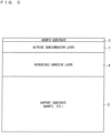
FIG. 2 , thenitride semiconductor layer 1 formed on thegrowth substrate 3 by a hetero epitaxial method and asupport substrate 5 as a substrate for temporarily holding thenitride semiconductor layer 1 are attached to each other via a reversibleadhesive layer 4 made up of a reversible adhesive agent. The reversible adhesive agent is an adhesive agent in which a cure state and a softened state can be switched by action of light or a temperature. For example, Japanese Patent Application Laid-OpenJP 2019- 26 817 A - After the
nitride semiconductor layer 1 and thesupport substrate 5 are attached to each other, processing of curing the reversibleadhesive layer 4 is performed for a purpose of increasing mechanical strength of the reversibleadhesive layer 4. A condition of curing the reversibleadhesive layer 4 is different depending on a reversible adhesive agent constituting the reversibleadhesive layer 4. For example, when the reversible adhesive agent made up of the liquid crystal polymer compound described above is used, the processing of curing the reversibleadhesive layer 4 can be performed by irradiating the reversibleadhesive layer 4 with visible light having a wavelength ranging from 420 nm to 600 nm. Glass, sapphire, silicon, and SiC, for example, can be used as a material of thesupport substrate 5, however, when the cure state and the softened state of the reversibleadhesive layer 4 is switched by irradiation with light, a material through which light used for curing and softening the reversibleadhesive layer 4 passes needs to be used for the material of thesupport substrate 5. - In the second step, as illustrated in
FIG. 3 , a portion on a back side of the growth substrate 3 (a side opposite to a surface thereof on which thenitride semiconductor layer 1 is formed) is removed to reduce a thickness of thegrowth substrate 3 to have a constant thickness. Mechanical grinding, dry etching, and etching by a solution, for example, can be used as a method of removing thegrowth substrate 3 in the second step, however, it is preferable to use the mechanical grinding from a viewpoint of a removal speed in the second step. The second step is preferably performed so that a thickness of the remaininggrowth substrate 3 is equal to or larger than 5 µm and smaller than 100 µm, and the thickness of the remaininggrowth substrate 3 is more preferably equal to or larger than 7 µm and smaller than 30 µm. - When the thickness of the remaining
growth substrate 3 after the second step is larger than that described above, a time required for the subsequent third step increases, and this increase leads to increase in manufacturing cost of thesemiconductor substrate 10. When the thickness of the remaininggrowth substrate 3 after the second step is smaller than that described above, inner stress of thenitride semiconductor layer 1 is reduced, and there is a high possibility of occurrence of a crack. - In the third step, as illustrated in
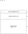
FIG. 4 , thegrowth substrate 3 whose thickness is reduced in the second step is completely removed to expose thenitride semiconductor layer 1. A mechanical polishing method, a chemical mechanical polishing method, a dry etching method, and etching by a solution, for example, can be used as a method of removing thegrowth substrate 3 in the third step, however, it is preferable to use the chemical mechanical polishing method in the third step. When the third step is performed by the chemical mechanical polishing method, a surface of the exposednitride semiconductor layer 1 is accurately flattened in an atomic layer level, thus strength after attaching thenitride semiconductor layer 1 and thenew substrate 2 is increased. - In the fourth step, the
new substrate 2 is attached to thenitride semiconductor layer 1 exposed in the third step. A substrate having a high thermal conductivity is preferable as thenew substrate 2 to improve performance and reliability of the nitride semiconductor element formed on thenitride semiconductor layer 1, and a diamond substrate is particularly preferable. - A surface activation bonding method and an atom diffusion bonding method, for example, can be used as a method of attaching the
nitride semiconductor layer 1 and thenew substrate 2, however, preferable is a method capable of reducing an interfacial thermal resistance between thenitride semiconductor layer 1 and thenew substrate 2 as much as possible to improve performance and reliability of the nitride semiconductor element. Thus, the surface activation bonding is particularly preferable. - When the surface activation bonding method is used, activation processing is performed on a surface of each of the
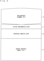
nitride semiconductor layer 1 and thenew substrate 2, and then thenitride semiconductor layer 1 and thenew substrate 2 are disposed to face each other and pressure-contacted as illustrated inFIG. 5 in a bonding device. At this time, when a warpage or a bulge of thenew substrate 2 is large, thenitride semiconductor layer 1 and thesupport substrate 5 are deformed along a surface shape of thenew substrate 2 as illustrated inFIG. 6 . - In the fifth step, processing for temporarily making the reversible
adhesive layer 4 be in a softened state is performed as illustrated inFIG. 7 while thenitride semiconductor layer 1 and thenew substrate 2 are pressure-contacted, and then processing of curing the reversibleadhesive layer 4 again is performed as illustrated inFIG. 8 . When the reversible adhesive agent made up of the liquid crystal polymer compound described above is used, the processing of softening the reversibleadhesive layer 4 can be performed by irradiating the reversibleadhesive layer 4 with ultraviolet light having a wavelength ranging from 300 nm to 400 nm via thesupport substrate 5, and the processing of curing the reversibleadhesive layer 4 can be performed by irradiating the reversibleadhesive layer 4 with visible light having a wavelength ranging from 420 nm to 600 nm via thesupport substrate 5. After the processing of curing the reversibleadhesive layer 4 is performed, pressure for forming bonding between thenitride semiconductor layer 1 and thenew substrate 2 is released, and a sample (a structure illustrated inFIG. 8 ) is taken out from the bonding device. - In the sixth step, as illustrated in
FIG. 9 , the reversibleadhesive layer 4 and thesupport substrate 5 are removed. As a result, thesemiconductor substrate 10 illustrated inFIG. 1 is completed. The sixth step can be performed by pulling off thesupport substrate 5 from thenitride semiconductor layer 1 by a physical method after making the reversibleadhesive layer 4 be in the softened state by irradiation with ultraviolet light via thesupport substrate 5, and subsequently immersing thenitride semiconductor layer 1 in an organic solvent, thereby removing the reversibleadhesive layer 4 from the surface of thenitride semiconductor layer 1. - Herein, an effect obtained in the present embodiment is described. For example, when an adhesive layer with no reversibility is used in place of the reversible
adhesive layer 4, the fifth step cannot be performed. In this case, when the pressure for forming bonding between thenitride semiconductor layer 1 and thenew substrate 2 is released, force of restoring thesupport substrate 5 which has been deformed in the fourth step to have an original shape is applied. This force acts to detach thenitride semiconductor layer 1 from thenew substrate 2, thus bonding cannot be formed in a region where this force exceeds bonding force between thenitride semiconductor layer 1 and thenew substrate 2. - For example, when the
new substrate 2 has a shape in which a center portion is thicker than a peripheral edge portion (when a cross-sectional shape of thenew substrate 2 is a convex lens-like shape), the force of restoring thesupport substrate 5 to have the original shape acts to detach thenitride semiconductor layer 1 from thenew substrate 2 in the peripheral edge portion of thenew substrate 2. - In contrast, in the present embodiment, the reversible
adhesive layer 4 is temporarily made to be in the softened state in the fifth step, thus inner stress of the reversibleadhesive layer 4 is released while thenitride semiconductor layer 1 and thenew substrate 2 are firmly attached to each other. Then, the deformation of thesupport substrate 5 occurring in the fourth step is resolved, and thesupport substrate 5 is restored to have the original shape. Accordingly, even when the pressure for forming bonding between thenitride semiconductor layer 1 and thenew substrate 2 is released, the force of restoring thesupport substrate 5 to have the original shape is not applied, but bonding between thenitride semiconductor layer 1 and thenew substrate 2 is maintained. Thus, even when a warpage or a bulge of thenew substrate 2 is large, the whole surfaces of thenitride semiconductor layer 1 and thenew substrate 2 can be uniformly bonded. - In the present embodiment, after the
nitride semiconductor layer 1 and thenew substrate 2 are pressure-contacted in the bonding device in the fourth step, the processing of temporarily making the reversibleadhesive layer 4 be in the softened state is performed in the fifth step, however, an order of performing them may be reversed. That is to say, it is also applicable that the reversibleadhesive layer 4 is previously made to be in the softened state, and thenitride semiconductor layer 1 and thenew substrate 2 are pressure-contacted in the bonding device in that state. - The
semiconductor substrate 10 manufactured by the manufacturing method according to the present embodiment can maintain a state where the whole surfaces of thenitride semiconductor layer 1 and thenew substrate 2 are uniformly bonded even when the diamond substrate having the large warpage is used as thenew substrate 2. Accordingly, a yield in the step of forming the nitride semiconductor element on thenitride semiconductor layer 1 can be improved. - When the
new substrate 2 functions as the heat radiation substrate, a heat radiation property of the nitride semiconductor element formed on thenitride semiconductor layer 1 can be increased, thus such a function can contribute to improvement of reliability of the nitride semiconductor element. - In the method of manufacturing the
semiconductor substrate 10 described in theEmbodiment 1, thesemiconductor substrate 10 is formed using thenitride semiconductor layer 1 in which the semiconductor elements such as an HEMT is not formed, however, in anEmbodiment 2, thesemiconductor substrate 10 is formed using thenitride semiconductor layer 1 in which the semiconductor element is formed in advance. - That is to say, the semiconductor element mounted to the semiconductor device is already incorporated into the
semiconductor substrate 10 manufactured by the method of manufacturing thesemiconductor substrate 10 according to theEmbodiment 2. Accordingly, the method of manufacturing thesemiconductor substrate 10 according to theEmbodiment 2 constitutes a part of the method of manufacturing the semiconductor device. - The method of manufacturing the
semiconductor substrate 10 according to theEmbodiment 2 is similar to that according to theEmbodiment 1 except that the semiconductor element is formed in advance in thenitride semiconductor layer 1 used in the first step.FIG. 2 to FIG. 9 described in theEmbodiment 1 are referenced also in the description of the method of manufacturing thesemiconductor substrate 10 according to theEmbodiment 2 described hereinafter. The description overlapped with that of theEmbodiment 1 is appropriately omitted. - Performed in the
Embodiment 2 is a step of forming the semiconductor element (nitride semiconductor element) on thenitride semiconductor layer 1 on thegrowth substrate 3 prior to the first step. An optional element may be applied to the semiconductor element formed in thenitride semiconductor layer 1, and an HEMT is formed in the present embodiment. An optional method may be applied to the method of forming the nitride semiconductor element, and applicable is a method disclosed in "AlGaN/GaN Heterojunction FETs for High Power Applications", IEICE Transactions on Electronics (Japanese Edition), Vol. J86-C, No. 4, pp. 396 to 403, April 2003, for example. - In the first step, as illustrated in
FIG. 2 , thenitride semiconductor layer 1 in which the semiconductor element is formed and thesupport substrate 5 are attached to each other via the reversibleadhesive layer 4 made up of the reversible adhesive agent of the liquid crystal polymer compound, for example. The, the processing of curing the reversibleadhesive layer 4 is performed for a purpose of increasing mechanical strength of the reversibleadhesive layer 4. - In the second step, as illustrated in
FIG. 3 , the portion on the back side of the growth substrate 3 (the side opposite to the surface thereof on which thenitride semiconductor layer 1 is formed) is removed by mechanical griding, for example, to reduce the thickness of thegrowth substrate 3 to have the constant thickness. - In the third step, as illustrated in
FIG. 4 , thegrowth substrate 3 whose thickness is reduced in the second step is completely removed by a chemical mechanical polishing method, for example, to expose thenitride semiconductor layer 1. - In the fourth step, the
new substrate 2 made of diamond, for example, is attached to thenitride semiconductor layer 1 exposed in the third step. When the surface activation bonding method is used, activation processing is performed on the surface of each of thenitride semiconductor layer 1 and thenew substrate 2, and then thenitride semiconductor layer 1 and thenew substrate 2 are disposed to face each other and pressure-contacted as illustrated inFIG. 5 in the bonding device. At this time, when the warpage or the bulge of thenew substrate 2 is large, thenitride semiconductor layer 1 and thesupport substrate 5 are deformed along the surface shape of thenew substrate 2 as illustrated inFIG. 6 . - In the fifth step, the processing for temporarily making the reversible
adhesive layer 4 be in a softened state is performed as illustrated inFIG. 7 while thenitride semiconductor layer 1 and thenew substrate 2 are pressure-contacted, and then the processing of curing the reversibleadhesive layer 4 again is performed as illustrated inFIG. 8 . Then, the pressure for forming bonding between thenitride semiconductor layer 1 and thenew substrate 2 is released, and the sample (the structure illustrated inFIG. 8 ) is taken out from the bonding device. - In the sixth step, as illustrated in
FIG. 9 , the reversibleadhesive layer 4 and thesupport substrate 5 are removed. As a result, thesemiconductor substrate 10 illustrated inFIG. 1 is completed. - Also in the present embodiment, after the
nitride semiconductor layer 1 and thenew substrate 2 are pressure-contacted in the bonding device in the fourth step, the processing of temporarily making the reversibleadhesive layer 4 be in the softened state is performed in the fifth step, however, the order of performing them may be reversed. That is to say, it is also applicable that the reversibleadhesive layer 4 is previously made to be in the softened state, and thenitride semiconductor layer 1 and thenew substrate 2 are pressure-contacted in the bonding device in that state. - The
semiconductor substrate 10 manufactured by the manufacturing method according to the present embodiment can maintain the state where the whole surfaces of thenitride semiconductor layer 1 and thenew substrate 2 are uniformly bonded even when the diamond substrate having the large warpage is used as thenew substrate 2. - Accordingly, the yield in the step of forming the nitride semiconductor element on the
nitride semiconductor layer 1 can be improved. When thenew substrate 2 functions as the heat radiation substrate, the heat radiation property of the nitride semiconductor element formed on thenitride semiconductor layer 1 can be increased, thus such a function can contribute to improvement of the reliability of the nitride semiconductor element. - Each embodiment can be arbitrarily combined, or each embodiment can be appropriately varied or omitted.
- The foregoing description is in all aspects illustrative, and is therefore understood that numerous modification examples not illustrated can be devised.
-
- 10 semiconductor substrate,
- 1 nitride semiconductor layer,
- 2 new substrate,
- 3 growth substrate,
- 4 reversible adhesive layer,
- 5 support substrate.
Claims (5)
- A method of manufacturing a semiconductor substrate, comprising:a step (a) of attaching a nitride semiconductor layer formed on a growth substrate and a support substrate via a reversible adhesive layer made up of a reversible adhesive agent and curing the reversible adhesive layer;a step (b) of removing the growth substrate to expose the nitride semiconductor layer after the step (a);a step (c) of bonding a new substrate to the nitride semiconductor layer after the step (b); anda step (d) of removing the reversible adhesive layer and the support substrate after the step (c), whereinthe step (c) includes:a step (c-1) of pressure-contacting the nitride semiconductor layer and the new substrate;a step (c-2) of softening the reversible adhesive layer; anda step (c-3) of curing the reversible adhesive layer again after the steps (c-1) and (c-2).
- The method of manufacturing the semiconductor substrate according to claim 1,
wherein the reversible adhesive agent is an adhesive agent in which a cure state and a softened state are switched by a wavelength of light with which the reversible adhesive agent is irradiated. - The method of manufacturing the semiconductor substrate according to claim 1 or 2,
wherein the step (c-2) is performed after the step (c-1). - The method of manufacturing the semiconductor substrate according to claim 1 or 2,
wherein the step (c-1) is performed after the step (c-2). - A method of manufacturing a semiconductor device, comprising:a step of performing the method of manufacturing the semiconductor substrate according to any one of claims 1 to 4,
and further comprisinga step (e) of forming a semiconductor element in the nitride semiconductor layer prior to the step (a).
Applications Claiming Priority (1)
| Application Number | Priority Date | Filing Date | Title |
|---|---|---|---|
| PCT/JP2021/004035 WO2022168217A1 (en) | 2021-02-04 | 2021-02-04 | Method for manufacturing semiconductor substrate and method for manufacturing semiconductor device |
Publications (2)
| Publication Number | Publication Date |
|---|---|
| EP4290553A1 true EP4290553A1 (en) | 2023-12-13 |
| EP4290553A4 EP4290553A4 (en) | 2024-04-03 |
Family
ID=82740968
Family Applications (1)
| Application Number | Title | Priority Date | Filing Date |
|---|---|---|---|
| EP21924614.7A Pending EP4290553A4 (en) | 2021-02-04 | 2021-02-04 | Method for manufacturing semiconductor substrate and method for manufacturing semiconductor device |
Country Status (6)
| Country | Link |
|---|---|
| US (1) | US20240030055A1 (en) |
| EP (1) | EP4290553A4 (en) |
| JP (1) | JP7475503B2 (en) |
| KR (1) | KR102760469B1 (en) |
| CN (1) | CN116868309A (en) |
| WO (1) | WO2022168217A1 (en) |
Family Cites Families (21)
| Publication number | Priority date | Publication date | Assignee | Title |
|---|---|---|---|---|
| JPH06268183A (en) | 1993-03-15 | 1994-09-22 | Fujitsu Ltd | Method for manufacturing semiconductor device |
| US6071795A (en) * | 1998-01-23 | 2000-06-06 | The Regents Of The University Of California | Separation of thin films from transparent substrates by selective optical processing |
| WO2002084631A1 (en) * | 2001-04-11 | 2002-10-24 | Sony Corporation | Element transfer method, element arrangmenet method using the same, and image display apparatus production method |
| US6911375B2 (en) * | 2003-06-02 | 2005-06-28 | International Business Machines Corporation | Method of fabricating silicon devices on sapphire with wafer bonding at low temperature |
| JP2005109208A (en) | 2003-09-30 | 2005-04-21 | Shin Etsu Handotai Co Ltd | Method of manufacturing light emitting element |
| EP1571705A3 (en) * | 2004-03-01 | 2006-01-04 | S.O.I.Tec Silicon on Insulator Technologies | Process of making a semiconductor structure on a substrate |
| JP4654389B2 (en) * | 2006-01-16 | 2011-03-16 | 株式会社ムサシノエンジニアリング | Room temperature bonding method for diamond heat spreader and heat dissipation part of semiconductor device |
| US20080122119A1 (en) * | 2006-08-31 | 2008-05-29 | Avery Dennison Corporation | Method and apparatus for creating rfid devices using masking techniques |
| FR2921515B1 (en) * | 2007-09-25 | 2010-07-30 | Commissariat Energie Atomique | METHOD FOR MANUFACTURING SEMICONDUCTOR STRUCTURES USEFUL FOR PRODUCING SEMICONDUCTOR-OVER-INSULATING SUBSTRATES, AND APPLICATIONS THEREOF |
| US8764026B2 (en) * | 2009-04-16 | 2014-07-01 | Suss Microtec Lithography, Gmbh | Device for centering wafers |
| JP5466578B2 (en) * | 2010-05-27 | 2014-04-09 | 株式会社神戸製鋼所 | Diamond-aluminum bonded body and manufacturing method thereof |
| WO2014095373A1 (en) * | 2012-12-18 | 2014-06-26 | Element Six Limited | Substrates for semiconductor devices |
| JP6004100B2 (en) * | 2013-05-24 | 2016-10-05 | 富士電機株式会社 | Manufacturing method of semiconductor device |
| JP5931803B2 (en) | 2013-06-10 | 2016-06-08 | 日本電信電話株式会社 | Manufacturing method of nitride semiconductor device |
| GB2544563B (en) * | 2015-11-20 | 2019-02-06 | Rfhic Corp | Mounting of semiconductor-on-diamond wafers for device processing |
| US10767088B2 (en) | 2016-01-07 | 2020-09-08 | National Institute Of Advanced Industrial Science And Technology | Photoreversible adhesive agent |
| GB201610886D0 (en) * | 2016-06-22 | 2016-08-03 | Element Six Tech Ltd | Bonding of diamond wafers to carrier substrates |
| JP2019527477A (en) | 2016-07-12 | 2019-09-26 | キューエムエイティ・インコーポレーテッド | Method for regenerating donor substrate |
| JP6671518B2 (en) | 2017-02-02 | 2020-03-25 | 三菱電機株式会社 | Semiconductor manufacturing method and semiconductor manufacturing apparatus |
| JP2019026817A (en) | 2017-08-04 | 2019-02-21 | 国立研究開発法人産業技術総合研究所 | Photoresponsive adhesive |
| KR102734318B1 (en) * | 2019-11-08 | 2024-11-25 | 에베 그룹 에. 탈너 게엠베하 | Substrate bonding device and method |
-
2021
- 2021-02-04 JP JP2022579226A patent/JP7475503B2/en active Active
- 2021-02-04 KR KR1020237021787A patent/KR102760469B1/en active Active
- 2021-02-04 WO PCT/JP2021/004035 patent/WO2022168217A1/en not_active Ceased
- 2021-02-04 EP EP21924614.7A patent/EP4290553A4/en active Pending
- 2021-02-04 CN CN202180092263.8A patent/CN116868309A/en active Pending
- 2021-02-04 US US18/265,434 patent/US20240030055A1/en active Pending
Also Published As
| Publication number | Publication date |
|---|---|
| KR20230116016A (en) | 2023-08-03 |
| WO2022168217A1 (en) | 2022-08-11 |
| CN116868309A (en) | 2023-10-10 |
| US20240030055A1 (en) | 2024-01-25 |
| JPWO2022168217A1 (en) | 2022-08-11 |
| KR102760469B1 (en) | 2025-01-24 |
| JP7475503B2 (en) | 2024-04-26 |
| EP4290553A4 (en) | 2024-04-03 |
Similar Documents
| Publication | Publication Date | Title |
|---|---|---|
| CN100474550C (en) | Substrate attaching method | |
| TW201214585A (en) | Method for manufacturing semiconductor device | |
| CN104145330A (en) | Method and apparatus for temporarily bonding ultra-thin wafers | |
| JP2013125971A (en) | Composite wafer for fabrication of semiconductor devices | |
| CN110858564A (en) | Method of processing substrate | |
| CN102403221A (en) | Manufacturing method of semiconductor element | |
| US20180019169A1 (en) | Backing substrate stabilizing donor substrate for implant or reclamation | |
| US8420505B2 (en) | Process for manufacture of thin wafer | |
| EP3485505A1 (en) | Method of a donor substrate undergoing reclamation | |
| CN113841223B (en) | Method for manufacturing semiconductor substrate and method for manufacturing semiconductor device | |
| EP4290553A1 (en) | Method for manufacturing semiconductor substrate and method for manufacturing semiconductor device | |
| CN120359595A (en) | Method for manufacturing semiconductor device | |
| WO2006043000A2 (en) | Method for transferring at least one micrometer or millimetre-sized object by means of a polymer handle | |
| US7981238B2 (en) | Method for relaxing a stressed thin film | |
| EP4138116B1 (en) | Method for manufacturing semiconductor element | |
| CN106415795B (en) | Method for producing large area solid layers | |
| CN112713099B (en) | Method for manufacturing semiconductor device | |
| Takigawa et al. | Low-temperature Au-to-Au bonding for LiNbO 3/Si structure achieved in ambient air | |
| US20230377935A1 (en) | Temporary bonding method | |
| US20240136324A1 (en) | Semiconductor manufacturing method | |
| CN118198035A (en) | Semiconductor wafer and method for processing semiconductor wafer | |
| CN120184047A (en) | Method for manufacturing semiconductor device | |
| TW202540351A (en) | A method for manufacturing a substrate, and substrate | |
| CN120569805A (en) | Method for manufacturing semiconductor device | |
| CN121361157A (en) | Method for forming wafer |
Legal Events
| Date | Code | Title | Description |
|---|---|---|---|
| STAA | Information on the status of an ep patent application or granted ep patent |
Free format text: STATUS: THE INTERNATIONAL PUBLICATION HAS BEEN MADE |
|
| PUAI | Public reference made under article 153(3) epc to a published international application that has entered the european phase |
Free format text: ORIGINAL CODE: 0009012 |
|
| STAA | Information on the status of an ep patent application or granted ep patent |
Free format text: STATUS: REQUEST FOR EXAMINATION WAS MADE |
|
| 17P | Request for examination filed |
Effective date: 20230724 |
|
| AK | Designated contracting states |
Kind code of ref document: A1 Designated state(s): AL AT BE BG CH CY CZ DE DK EE ES FI FR GB GR HR HU IE IS IT LI LT LU LV MC MK MT NL NO PL PT RO RS SE SI SK SM TR |
|
| A4 | Supplementary search report drawn up and despatched |
Effective date: 20240305 |
|
| RIC1 | Information provided on ipc code assigned before grant |
Ipc: H01L 29/812 20060101ALI20240228BHEP Ipc: H01L 29/778 20060101ALI20240228BHEP Ipc: H01L 21/338 20060101ALI20240228BHEP Ipc: H01L 21/02 20060101AFI20240228BHEP |
|
| DAV | Request for validation of the european patent (deleted) | ||
| DAX | Request for extension of the european patent (deleted) |