EP4290386A1 - Packet cache system and method - Google Patents
Packet cache system and method Download PDFInfo
- Publication number
- EP4290386A1 EP4290386A1 EP22207008.8A EP22207008A EP4290386A1 EP 4290386 A1 EP4290386 A1 EP 4290386A1 EP 22207008 A EP22207008 A EP 22207008A EP 4290386 A1 EP4290386 A1 EP 4290386A1
- Authority
- EP
- European Patent Office
- Prior art keywords
- cache memory
- packet
- memory
- cache
- memory address
- Prior art date
- Legal status (The legal status is an assumption and is not a legal conclusion. Google has not performed a legal analysis and makes no representation as to the accuracy of the status listed.)
- Granted
Links
Images


Classifications
-
- G—PHYSICS
- G06—COMPUTING OR CALCULATING; COUNTING
- G06F—ELECTRIC DIGITAL DATA PROCESSING
- G06F12/00—Accessing, addressing or allocating within memory systems or architectures
- G06F12/02—Addressing or allocation; Relocation
- G06F12/08—Addressing or allocation; Relocation in hierarchically structured memory systems, e.g. virtual memory systems
- G06F12/0802—Addressing of a memory level in which the access to the desired data or data block requires associative addressing means, e.g. caches
- G06F12/0893—Caches characterised by their organisation or structure
- G06F12/0895—Caches characterised by their organisation or structure of parts of caches, e.g. directory or tag array
-
- G—PHYSICS
- G06—COMPUTING OR CALCULATING; COUNTING
- G06F—ELECTRIC DIGITAL DATA PROCESSING
- G06F12/00—Accessing, addressing or allocating within memory systems or architectures
- G06F12/02—Addressing or allocation; Relocation
- G06F12/08—Addressing or allocation; Relocation in hierarchically structured memory systems, e.g. virtual memory systems
- G06F12/0802—Addressing of a memory level in which the access to the desired data or data block requires associative addressing means, e.g. caches
- G06F12/0864—Addressing of a memory level in which the access to the desired data or data block requires associative addressing means, e.g. caches using pseudo-associative means, e.g. set-associative or hashing
-
- G—PHYSICS
- G06—COMPUTING OR CALCULATING; COUNTING
- G06F—ELECTRIC DIGITAL DATA PROCESSING
- G06F12/00—Accessing, addressing or allocating within memory systems or architectures
- G06F12/02—Addressing or allocation; Relocation
- G06F12/08—Addressing or allocation; Relocation in hierarchically structured memory systems, e.g. virtual memory systems
- G06F12/0802—Addressing of a memory level in which the access to the desired data or data block requires associative addressing means, e.g. caches
- G06F12/0866—Addressing of a memory level in which the access to the desired data or data block requires associative addressing means, e.g. caches for peripheral storage systems, e.g. disk cache
-
- G—PHYSICS
- G06—COMPUTING OR CALCULATING; COUNTING
- G06F—ELECTRIC DIGITAL DATA PROCESSING
- G06F12/00—Accessing, addressing or allocating within memory systems or architectures
- G06F12/02—Addressing or allocation; Relocation
- G06F12/08—Addressing or allocation; Relocation in hierarchically structured memory systems, e.g. virtual memory systems
- G06F12/0802—Addressing of a memory level in which the access to the desired data or data block requires associative addressing means, e.g. caches
- G06F12/0866—Addressing of a memory level in which the access to the desired data or data block requires associative addressing means, e.g. caches for peripheral storage systems, e.g. disk cache
- G06F12/0868—Data transfer between cache memory and other subsystems, e.g. storage devices or host systems
-
- G—PHYSICS
- G06—COMPUTING OR CALCULATING; COUNTING
- G06F—ELECTRIC DIGITAL DATA PROCESSING
- G06F12/00—Accessing, addressing or allocating within memory systems or architectures
- G06F12/02—Addressing or allocation; Relocation
- G06F12/08—Addressing or allocation; Relocation in hierarchically structured memory systems, e.g. virtual memory systems
- G06F12/12—Replacement control
- G06F12/121—Replacement control using replacement algorithms
-
- G—PHYSICS
- G06—COMPUTING OR CALCULATING; COUNTING
- G06F—ELECTRIC DIGITAL DATA PROCESSING
- G06F12/00—Accessing, addressing or allocating within memory systems or architectures
- G06F12/02—Addressing or allocation; Relocation
- G06F12/08—Addressing or allocation; Relocation in hierarchically structured memory systems, e.g. virtual memory systems
- G06F12/12—Replacement control
- G06F12/121—Replacement control using replacement algorithms
- G06F12/123—Replacement control using replacement algorithms with age lists, e.g. queue, most recently used [MRU] list or least recently used [LRU] list
-
- G—PHYSICS
- G06—COMPUTING OR CALCULATING; COUNTING
- G06F—ELECTRIC DIGITAL DATA PROCESSING
- G06F12/00—Accessing, addressing or allocating within memory systems or architectures
- G06F12/02—Addressing or allocation; Relocation
- G06F12/08—Addressing or allocation; Relocation in hierarchically structured memory systems, e.g. virtual memory systems
- G06F12/12—Replacement control
- G06F12/121—Replacement control using replacement algorithms
- G06F12/126—Replacement control using replacement algorithms with special data handling, e.g. priority of data or instructions, handling errors or pinning
-
- G—PHYSICS
- G06—COMPUTING OR CALCULATING; COUNTING
- G06F—ELECTRIC DIGITAL DATA PROCESSING
- G06F2212/00—Indexing scheme relating to accessing, addressing or allocation within memory systems or architectures
- G06F2212/10—Providing a specific technical effect
- G06F2212/1016—Performance improvement
-
- G—PHYSICS
- G06—COMPUTING OR CALCULATING; COUNTING
- G06F—ELECTRIC DIGITAL DATA PROCESSING
- G06F2212/00—Indexing scheme relating to accessing, addressing or allocation within memory systems or architectures
- G06F2212/15—Use in a specific computing environment
- G06F2212/154—Networked environment
Definitions
- packets may be transmitted from a node, and received at a node, faster than they can be processed.
- ASICs application-specific integrated circuits
- packets may be received by the ASIC faster than they can be processed, and may be transmitted by the ASIC faster than receive-acknowledgements can be received at the ASIC from the intended recipient.
- the packets need to be temporarily stored while they await processing. For instance, packets transmitted by an ASIC need to be stored at the ASIC until receipt is acknowledged. Further, in order to maximize the speed at which a node operates, temporarily stored packets should be stored in cache memory whenever possible.
- a packet cache configuration provides efficient data management for spillover from cache memory to non-cache memory (e.g., on-chip SRAM to off-chip DRAM), and provides a transparent interface to the user independent of the data storage location (e.g., on-chip or off-chip).
- the technology provides a packet cache system including a cache memory allocator for receiving a memory address corresponding to a non-cache memory and allocated to a packet, and associating the memory address with a cache memory address; a hash table for storing the memory address and the cache memory address, with the memory address as a key and the cache memory address as a value; a cache memory for storing the packet at a location indicated by the cache memory address; and an eviction engine for determining one or more cached packets to remove from the cache memory and place in the non-cache memory when occupancy of the cache memory is high.
- the technology provides a method for storing packets in a cache memory of a device, including allocating a memory address, corresponding to a non-cache memory, to a packet; associating the memory address with a cache memory address; storing the memory address and the cache memory address in a hash table, with the memory address as a key and the cache memory address as a value; storing the packet in cache memory at a location indicated by the cache memory address; and when occupancy of the cache memory is high, determining one or more cached packets to remove from the cache memory and place in the non-cache memory.
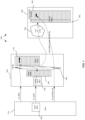
- Fig. 1 is a block diagram of a packet cache system 100 and a packet cache system user 110 according to an embodiment, in which the flow of write information is depicted.
- the system hardware is optimized when packets stored in the system are handled in one or more fixed size units, and thus the system 100 is described in the context of packets being divided into 256 byte units called cells.
- the system 100 stores and manages cells for packets received in both a cache memory 115 (e.g., an on-chip static random-access memory, SRAM) and a non-cache memory (not shown) (e.g., off-chip dynamic random-access memory, DRAM) based on occupancy of the cache memory 115 and other parameters.
- a cache memory 115 e.g., an on-chip static random-access memory, SRAM
- a non-cache memory not shown
- DRAM off-chip dynamic random-access memory
- the system 100 manages the eviction of cells from the cache memory 115 to the non-cache memory, and read/write transactions from the user 110 are handled transparently from the perspective of the user 110, irrespective of whether the data being read/written is stored in the cache memory 115 or the non-cache memory. Moreover, in some embodiments, the system 100 stores data in the cache memory 115 in 64B flits (flow control units/flow control digits).
- the packet cache system 100 may include an eviction engine 120 to move data from the cache memory 115 to non-cache memory based on occupancy of the cache memory 115 and packet priority.
- the eviction engine 120 may also use the age of cache memory 115 entries as a factor in determining whether a packet may be evicted.
- the eviction engine 120 attempts to ensure that the cache memory 115 has space to accommodate write requests from user 110. In rare cases that eviction is not fast enough to accommodate write requests, the write request interface will be back-pressured.
- the packet cache system 100 of Fig. 1 has a cache subsystem 125.
- the cache subsystem 125 includes a cache memory allocator 130 for receiving a memory address corresponding to a non-cache memory and allocated to a packet, and a hash table 135 for associating the memory address with a cache memory address corresponding to a location in the cache memory 115.
- the packet, or part of the packet may be stored in the cache memory 115 at a location indicated by the cache memory address.
- the memory address may be hashed to hash table location in the hash table 135 by applying a hash function to the memory address, and the cache memory address may be stored in the hash table 135 at the hash table location.
- Operations within the cache subsystem 125 may be controlled according to a finite state machine (FSM) 140.
- FSM finite state machine
- both the memory address and the cache memory address for a packet or cell data may be stored at a location in the hash table 135 as a "key-value pair.”
- Such configuration facilitates use of the memory address (or key) to locate the cache memory address(es) of a desired packet when the hash table 135 is used to store multiple cache memory addresses at each location of the hash table 135.
- the cache memory 115 may be organized in four banks, and the cache memory allocator 130 may allocate a branch of memory addresses according to the length of write data, at a rate of up to four addresses per cycle.
- each packet in the cache memory 115 may correspond on a one-to-one basis with a priority memory entry in a priority memory 145 of the eviction engine 120.
- a packet or cell is assigned a cache memory address in cache memory 115 and is stored in the cache memory 115 at the cache memory address
- the packet or cell is assigned a corresponding priority memory address in the priority memory 145 and a priority for the packet or cell is stored at the corresponding priority memory address.
- a valid/invalid indicator (e.g., a valid/invalid bit) is stored with the priority, as indicated by a validity section 150 of the priority memory 145.
- the eviction engine 120 uses eviction logic 155 to initiate and conduct an evict scan, when occupancy of the cache memory 115 is high, although an evict scan can also be triggered by the user 110 through an evict interface (not shown).
- evict logic 155 When a packet or cell is evicted/deallocated from the cache memory 115, its corresponding valid/invalid indicator is set to invalid.
- the Fig. 1 embodiment further includes a memory allocator 160 for allocating non-cache memory addresses to packets.
- the memory allocator 160 is shown as part of the user 110; however, it should be noted that in some embodiments the memory allocator 160 may be part of the packet cache system 100.
- the packet cache system 100 supports the following features:
- each cell may be associated with a non-cache memory address (e.g., a DRAM address).
- Each cell may include 256B. Further, each cell may be in one of 3 formats:
- the packet will fit in one control cell with inline payload. If a packet cannot fit into one cell, the packet will use a first cell as a control cell with payload pointers, and packet data will be stored in data cells.
- a packet is subjected to a write, read, deallocate process. For example, a packet received by user 110 is written to cache memory 115 while the packet awaits processing, then during processing the packet is read from the cache memory 115 multiple times, and when the processing for the packet is complete the space in the cache memory 115 that was allocated to the packet is deallocated.
- the write process contains the following steps:
- the read process contains the following steps:
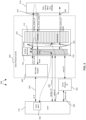
- FIG. 2 the figure is a block diagram of the packet cache system 100 and the packet cache system user 110 of Fig. 1 , in which the flow of deallocation information is depicted.
- the deallocate process contains the following steps:
- the evict process contains the following steps:
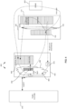
- the figure is a block diagram of a packet cache system 300, the packet cache system user 110, and a non-cache memory 310 according to an embodiment.
- the packet cache system 300 has six interfaces, a non-cache memory read interface 315, a non-cache memory write interface 320, an evict request interface 325, a write interface 330, the deallocation interface 205, and a read interface 335.
- the read interface couples the user 110 to a reorder engine 340 which, in turn, may include and maintain the ROB.
- the reorder engine 340 serves to reorder read responses from the cache memory 115 and non-cache memory 310, as necessary.
- the reorder engine 340 and cache subsystem 125 define a data packet cache 350.
- the data packet cache 350, the evict engine 120 and the user 110 are parts of a single integrated circuit chip, and the non-cache memory 310 is external to the chip.
- the data packet cache 350, the evict engine 120 and the user 110 are part of an ASIC, with the user 110 being a TX/RX module of the ASIC, the cache memory being SRAM internal to the chip, and the non-cache memory 310 being DRAM external to the chip.
- the data packet cache 350 includes the cache memory 115 to store packets on-chip, the cache memory allocator 130 to allocate available space in cache memory 115 when a write event happens, the reorder engine 340 to reorder read responses from either cache memory 115 or non-cache memory 310, the hash table 135 to remember the mapping between non-cache memory addresses and cache memory addresses, and the finite state machine 140 to manage all the flows.
- the user 110 will initiate read, write, deallocate events to the data packet cache 350, while the eviction engine 120 handles priority/age based evictions.
- the reorder engine 340 it will record the order of all read requests and return all read responses in the same order, no matter whether the data is from the cache memory 115 or the non-cache memory 310.
- Fig. 4 is a block diagram of a packet cache system 400, a TX/RX controller 410, and DRAM 420 according to an embodiment, in which elements of a reorder engine 430 are depicted.
- the TX/RX 410 is a packet cache system user
- the DRAM 420 is a non-cache memory
- the reorder engine 430 may include a register 470.
- the register 470 is used to store data read prior to such data being sent from the reorder engine 430 to the TX/RX controller 410.
- the reorder engine FSM 460 may include a multiplexer function 480 for switching between supplying data from the reorder buffer 440 and the register 470.
- Fig. 5 the figure is a flowchart describing operation of the reorder engine 430 according to an embodiment.
- Fig. 5 is described in reference to the Fig. 4 configuration.
- a determination is made as to whether the received read request corresponds to a connection ID that matches the connection ID of a pending read request for which DRAM 420 is being read (step 510).
- the received read request corresponds to a connection ID that matches the connection ID of a pending DRAM read request
- the received read request is sent to the request array 450 of the reorder engine 430 for handling (step 520), and the reorder engine 430 will reorder the out-of-order responses to make sure TX/RX controller 410 sees the read responses for same connection in order.
- the reorder engine 430 may send the data for the received read request to the TX/RX controller 410 (step 540).
- step 510 If, in step 510, it is determined that the received read request does not correspond to a connection ID that matches the connection ID of a pending read request for which DRAM 420 is being read, then a lookup is performed in the hash table 135 for the dram_cell_addr of the first cell (or only cell) for the received read request (step 550), and a determination is made as to whether or not the lookup results in a hash table miss (step 560).
- step 520 the operation proceeds to step 520, with the received read request being sent to the request array 450 for handling so as to avoid the data for the read request being provided to the TX/RX controller out of order (e.g., due to slow speed of retrieval of the data from DRAM 420).
- step 550 If the lookup of step 550 results in a hash table hit, the data corresponding to the received read request is read from the cache memory 115 and stored in the register 470, without the read request being sent to the request array 450 (step 570). Following receipt of all the data by the register 470, the reorder engine 430 sends the data for the received read request to the TX/RX controller 410 (step 540).
- Embodiments of the present technology include, but are not restricted to, the following.
Landscapes
- Engineering & Computer Science (AREA)
- Theoretical Computer Science (AREA)
- Physics & Mathematics (AREA)
- General Engineering & Computer Science (AREA)
- General Physics & Mathematics (AREA)
- Memory System Of A Hierarchy Structure (AREA)
Abstract
Description
- Two important attributes of packet-based communication systems are speed and reliability. In many such systems, packets may be transmitted from a node, and received at a node, faster than they can be processed. For example, in packet-based communication with an application-specific integrated circuits (ASICs) packets may be received by the ASIC faster than they can be processed, and may be transmitted by the ASIC faster than receive-acknowledgements can be received at the ASIC from the intended recipient. Accordingly, to ensure proper handling of packets at a node, the packets need to be temporarily stored while they await processing. For instance, packets transmitted by an ASIC need to be stored at the ASIC until receipt is acknowledged. Further, in order to maximize the speed at which a node operates, temporarily stored packets should be stored in cache memory whenever possible.
- It has been recognized that achieving high-level communication performance at a node of a packet-based communication system, even under drop and congestion scenarios, requires efficient storage support for a large number of outstanding packets where each request could be as large as Maximum Transmission Unit (MTU) size. In view of the desire for efficient packet storage support, the presently disclosed technology is provided.
- In accordance with the presently disclosed technology a packet cache configuration provides efficient data management for spillover from cache memory to non-cache memory (e.g., on-chip SRAM to off-chip DRAM), and provides a transparent interface to the user independent of the data storage location (e.g., on-chip or off-chip).
- In one aspect, the technology provides a packet cache system including a cache memory allocator for receiving a memory address corresponding to a non-cache memory and allocated to a packet, and associating the memory address with a cache memory address; a hash table for storing the memory address and the cache memory address, with the memory address as a key and the cache memory address as a value; a cache memory for storing the packet at a location indicated by the cache memory address; and an eviction engine for determining one or more cached packets to remove from the cache memory and place in the non-cache memory when occupancy of the cache memory is high.
- In another aspect, the technology provides a method for storing packets in a cache memory of a device, including allocating a memory address, corresponding to a non-cache memory, to a packet; associating the memory address with a cache memory address; storing the memory address and the cache memory address in a hash table, with the memory address as a key and the cache memory address as a value; storing the packet in cache memory at a location indicated by the cache memory address; and when occupancy of the cache memory is high, determining one or more cached packets to remove from the cache memory and place in the non-cache memory.
- The accompanying drawings are not intended to be drawn to scale. Also, for purposes of clarity not every component may be labeled in every drawing. In the drawings:
-
Fig. 1 is a block diagram of a packet cache system and a packet cache system user according to an embodiment, in which the flow of write information is depicted. -
Fig. 2 is a block diagram of the packet cache system and the packet cache system user ofFig. 1 , in which the flow of deallocation information is depicted. -
Fig. 3 is a block diagram of a packet cache system, a packet cache system user, and a non-cache memory according to an embodiment. -
Fig. 4 is a block diagram of a packet cache system, a packet cache system user, and a non-cache memory according to an embodiment, in which elements of a reorder engine embodiment are depicted. -
Fig. 5 is a flowchart describing the handling of a user read request according to a reorder engine of an embodiment. - Examples of systems and methods are described herein. It should be understood that the words "example," "exemplary" and "illustrative" are used herein to mean "serving as an example, instance, or illustration." Any embodiment or feature described herein as being an "example," "exemplary" or "illustration" is not necessarily to be construed as preferred or advantageous over other embodiments or features. In the following description, reference is made to the accompanying figures, which form a part thereof. In the figures, similar symbols typically identify similar components, unless context dictates otherwise. Other embodiments may be utilized, and other changes may be made, without departing from the spirit or scope of the subject matter presented herein.
- The example embodiments described herein are not meant to be limiting. It will be readily understood that the aspects of the present disclosure, as generally described herein, and illustrated in the figures, can be arranged, substituted, combined, separated, and designed in a wide variety of different configurations, all of which are explicitly contemplated herein.
-
Fig. 1 is a block diagram of apacket cache system 100 and a packetcache system user 110 according to an embodiment, in which the flow of write information is depicted. The system hardware is optimized when packets stored in the system are handled in one or more fixed size units, and thus thesystem 100 is described in the context of packets being divided into 256 byte units called cells. Thesystem 100 stores and manages cells for packets received in both a cache memory 115 (e.g., an on-chip static random-access memory, SRAM) and a non-cache memory (not shown) (e.g., off-chip dynamic random-access memory, DRAM) based on occupancy of thecache memory 115 and other parameters. Thesystem 100 manages the eviction of cells from thecache memory 115 to the non-cache memory, and read/write transactions from theuser 110 are handled transparently from the perspective of theuser 110, irrespective of whether the data being read/written is stored in thecache memory 115 or the non-cache memory. Moreover, in some embodiments, thesystem 100 stores data in thecache memory 115 in 64B flits (flow control units/flow control digits). - The
packet cache system 100 may include aneviction engine 120 to move data from thecache memory 115 to non-cache memory based on occupancy of thecache memory 115 and packet priority. Theeviction engine 120 may also use the age ofcache memory 115 entries as a factor in determining whether a packet may be evicted. Theeviction engine 120 attempts to ensure that thecache memory 115 has space to accommodate write requests fromuser 110. In rare cases that eviction is not fast enough to accommodate write requests, the write request interface will be back-pressured. - The
packet cache system 100 ofFig. 1 has acache subsystem 125. Thecache subsystem 125 includes acache memory allocator 130 for receiving a memory address corresponding to a non-cache memory and allocated to a packet, and a hash table 135 for associating the memory address with a cache memory address corresponding to a location in thecache memory 115. The packet, or part of the packet, may be stored in thecache memory 115 at a location indicated by the cache memory address. The memory address may be hashed to hash table location in the hash table 135 by applying a hash function to the memory address, and the cache memory address may be stored in the hash table 135 at the hash table location. In this manner, one may rapidly search out the packet from thecache memory 115 based on the memory address of the packet (e.g., in response to a read request) by hashing the memory address to a location in the hash table 135, noting the cache memory address from the location in the hash table 135, and accessing thecache memory 115 based on the noted address. Operations within thecache subsystem 125 may be controlled according to a finite state machine (FSM) 140. - In some embodiments, both the memory address and the cache memory address for a packet or cell data may be stored at a location in the hash table 135 as a "key-value pair." Such configuration facilitates use of the memory address (or key) to locate the cache memory address(es) of a desired packet when the hash table 135 is used to store multiple cache memory addresses at each location of the hash table 135.
- In embodiments employing 256B cells and 64B flits, the
cache memory 115 may be organized in four banks, and thecache memory allocator 130 may allocate a branch of memory addresses according to the length of write data, at a rate of up to four addresses per cycle. - In any event, each packet in the
cache memory 115 may correspond on a one-to-one basis with a priority memory entry in apriority memory 145 of theeviction engine 120. When a packet or cell is assigned a cache memory address incache memory 115 and is stored in thecache memory 115 at the cache memory address, the packet or cell is assigned a corresponding priority memory address in thepriority memory 145 and a priority for the packet or cell is stored at the corresponding priority memory address. A valid/invalid indicator (e.g., a valid/invalid bit) is stored with the priority, as indicated by avalidity section 150 of thepriority memory 145. Theeviction engine 120 useseviction logic 155 to initiate and conduct an evict scan, when occupancy of thecache memory 115 is high, although an evict scan can also be triggered by theuser 110 through an evict interface (not shown). When a packet or cell is evicted/deallocated from thecache memory 115, its corresponding valid/invalid indicator is set to invalid. - The
Fig. 1 embodiment further includes amemory allocator 160 for allocating non-cache memory addresses to packets. Thememory allocator 160 is shown as part of theuser 110; however, it should be noted that in some embodiments thememory allocator 160 may be part of thepacket cache system 100. - The
packet cache system 100 supports the following features: - Store data in the cache memory 115 (e.g., SRAM on-chip memory) in flits of 64B.
- Work with the
eviction engine 120 to move data fromcache memory 115 to non-cache memory (e.g., DRAM off-chip memory), based on cache occupancy and packet priority. - Interface for Write, Read, Deallocation, and Eviction on a packet basis.
- ∘ Accept write data cells for each packet and track cells that belong to a packet.
- ∘ Eviction is also managed on a packet basis and all cells for a given packet reside either in
cache memory 115 or in non-cache memory - ∘ Upon one read request with the non-cache memory address pointing to a control cell, the
packet cache system 100 reads back all data cells for the packet. - ∘ Upon one deallocation request with the non-cache memory address pointing to the control cell, the
packet cache system 100 deallocates all data cells for the packet.
- Re-order read data cells per packet/per connection.
- The
cache subsystem 125 is fully associative and uses the hash table 135 for lookup. - Write back policy which ensures that the non-cache memory bandwidth is conserved. Data is written back to non-cache memory only when a packet is evicted from the
cache memory 115. - Regarding the dividing of packets into cells, each cell may be associated with a non-cache memory address (e.g., a DRAM address). Each cell may include 256B. Further, each cell may be in one of 3 formats:
- Control cell with inline payload - having the following components:
- ∘ Packet info
- ∘ Packet Meta Data (PMD) to be sent to Upper Level Protocol (ULP)
- ∘ Packet data
- Control cell with payload pointers - having the following components:
- ∘ Packet info
- ∘ PMD to be sent to ULP
- ∘ Packet data pointers to all cells' non-cache memory addresses
- Data cell - has only a single component:
- ∘ Packet data
- If a packet can fit into one cell, the packet will fit in one control cell with inline payload. If a packet cannot fit into one cell, the packet will use a first cell as a control cell with payload pointers, and packet data will be stored in data cells.
- In general, a packet is subjected to a write, read, deallocate process. For example, a packet received by
user 110 is written tocache memory 115 while the packet awaits processing, then during processing the packet is read from thecache memory 115 multiple times, and when the processing for the packet is complete the space in thecache memory 115 that was allocated to the packet is deallocated. - The write process contains the following steps:
-
User 110, e.g., a transmit/receive (TX/RX) module of an ASIC, generates the write request, including:- ∘ Assemble data in required format
- ∘ For each cell of the assembled data, send a free address for non-cache memory space (for purposes of this description, these addresses will be called dram_cell_addr)
- ∘ Set initial priority level for current packet
- ∘ Set start-of-packet/end-of-packet (sop/eop) indicators to demarcate the packet within the write request
- The
cache subsystem 125 will assemble the packet into write data (wr data) of fixed-size cells and store these cells in the cache memory 115:- ∘ Get available cache memory addresses from the cache memory allocator 130 (call these addresses cache_addr)
- ∘ For each cell of the assembled write data, install the hash table 135 with dram_cell_addr as key and cache addr as value
- ∘ Store cells to the
cache memory 115 at cache _addr - ∘ If sop is set and this is the first flit, send an install request to the
eviction engine 120 with initial priority level for the packet (sop will be set for the 1st cell of a packet; e.g., a large packet might be broken down to several cells, among which the first cell has sop=1 and last cell has eop=1) - ∘ Send back write response to user - if a write is successful the
cache subsystem 125 sends the user 110 a write response indicating that the write is successful; if there is not enough space incache memory 115 to accommodate the write request, thecache subsystem 125 back-pressures theuser 110 to indicate that the write request cannot be accommodated (cache subsystem 125 may resume to accept writes to the cache memory once space is available due to deallocate/evict)
- The read process contains the following steps:
-
User 110, e.g., a transmit/receive (TX/RX) module of an ASIC, generates the read request, including:- ∘ Send first data cell's address which is previously assigned by
memory allocator 160 during write (called as dram_cell_addr) tocache subsystem 125 - ∘ Provide expected data length to
cache subsystem 125
- ∘ Send first data cell's address which is previously assigned by
- The
cache subsystem 125 will assemble the read data (rd_data) properly according to read interface requirements and return all read data for read requests in the order in which the read requests are received at the cache subsystem (It is noted that there could be multiple connections and each connection will have multiple packets to be read; and that within the same connection, the read responses are in the order in which the read requests are received, but between different connections, the read response might be out of order):- ∘ Store read requests and cookies in a reorder buffer (ROB)
- ∘ Do a hash table lookup in hash table 135 for the first data cell's dram_cell_addr
- ▪ If hit
- Read the corresponding entry from
cache memory 115 according to cache memory addresses returned from with hash table 135 and link the read entry to the corresponding ROB request (The reorder buffer entry is packet based; the response might contain multiple cells, but all the cells should belong to one packet) - If the expected data length is no more than 1 cell long, mark the corresponding ROB request as done; if the expected data length is more than 1 cell long, decode the first cell, get the data pointers for the dram_cell_addr of other cells
- Repeat the hash table lookup/cache memory read process until all data pointers are read out from data memory, then mark the read done in the ROB
- Read the corresponding entry from
- ▪ If miss
- Read the corresponding entry from non-cache memory and link the read entry to the corresponding ROB request
- If the expected data length is no more than 1 cell long, mark the corresponding ROB request as done; if the expected data length is more than 1 cell long, decode the first cell, get the data pointers for the dram cell addr addresses of other cells
- Read data from non-cache memory according to the dram cell addr addresses of the other cells, then mark the read done in the ROB
- ▪ If hit
- ∘ Based on the ROB, send to the
user 110 the read data for the oldest read request pertaining to the same connection as the current read request when the current read is done; or, if there is no older read request pertaining to the same connection as the current read request, send to theuser 110 the read data for the current read request as soon as the current read is done
- Turning now to
Fig. 2 , the figure is a block diagram of thepacket cache system 100 and the packetcache system user 110 ofFig. 1 , in which the flow of deallocation information is depicted. - The deallocate process contains the following steps:
-
User 110, e.g., a transmit/receive (TX/RX) module of an ASIC, generates a deallocate request corresponding to a packet to thecache subsystem 125 through adeallocation interface 205, including:- ∘ send first data cell's address which is previously assigned by the
memory allocator 160 during write (dram_cell_addr) - ∘ provide expected data length
- ∘ send first data cell's address which is previously assigned by the
- The
cache subsystem 125 will deallocate memory space allocated to the packet and respond to the user according todeallocate interface 205 requirements:- ∘ Do a lookup in hash table 135 for the first cell's dram_cell_addr
- ▪ If hit
- Read out the 1st data cell from
cache memory 115 - If there is more than one cell, get the data pointers for the other cell(s) and do a lookup in hash table 135 for each additional cell to get the corresponding cache memory addresses
- For all above lookups
- ∘ Return the cache memory address to
cache memory allocator 130 as an available cache memory address so that thecache memory allocator 130 can re-use the cache memory address - ∘ Return non-cache memory address to the
memory allocator 160 so that thememory allocator 160 can re-use the non-cache memory addresses - ∘ Update the hash table 135, i.e., removing the entry corresponding to the deallocated cache memory address
- ∘ Generate an
uninstall request 210 to theeviction engine 120 so that theeviction engine 120 can mark as invalid the entry inpriority memory 145 that corresponds to the deallocated cache memory address
- ∘ Return the cache memory address to
- Read out the 1st data cell from
- ▪ If miss
- Read out the 1st data cell from non-cache memory
- If more than one cell, get the data pointers for other cell(s), and
- For all non-cache memory addresses, either one address corresponding to the 1st cell or to multiple addresses corresponding to the 1st cell and one or more other cells, return the addresses to the
memory allocator 160 so that the memory allocator can re-use the addresses
- ▪ If hit
- ∘ Do a lookup in hash table 135 for the first cell's dram_cell_addr
- Regarding eviction, no matter how many cells one packet has, all cells will be evicted together. Thus, all cells for a packet will be either in the
cache memory 115 or in the non-cache memory. - The evict process contains the following steps:
- The
eviction engine 120 determines which packet to be evicted and assembles the evict request, including:- ∘
Eviction engine 120 will initiate an evict scan according to theeviction logic 155 when occupancy of thecache memory 115 is high; theeviction engine 120 will determine which packet to be evicted from thecache memory 115 to non-cache memory according to an eviction engine evict mechanism - ∘ Eviction can also be triggered directly by the
user 110 request through an evict interface between the user and theeviction engine 120 - ∘ Once a packet is selected for eviction, the
eviction engine 120 will send the non-cache memory address for the first cell of the packet to thecache subsystem 125
- ∘
- The
cache subsystem 125 will evict the entire packet:- ∘ Do a lookup in the hash table 135 for the non-cache memory address of the first cell
- ▪ If hit
- Read out the 1st data cell from
cache memory 115 - If there is more than one cell, get the data pointers for the other cell(s) and do a lookup in hash table 135 for each additional cell to get the corresponding cache memory addresses
- For all above lookups
- ∘ Return the cache memory address to
cache memory allocator 130 as an available cache memory address so that thecache memory allocator 130 can re-use the cache memory address - ∘ read out the data from the cache memory address and write the data to the non-cache memory address:
- ▪ Reformat data and address according to the requirements of the non-cache memory interface
- ∘ Update the hash table 135 to remove the entry corresponding to the cache memory address of the evicted cell
- ∘ Return the cache memory address to
- Read out the 1st data cell from
- ▪ If miss
- miss means a racing case exists, i.e., the space in
cache memory 115 corresponding to the packet designated for eviction was deallocated just before the eviction of the packet; so, the eviction process can be marked as done in response to the miss
- miss means a racing case exists, i.e., the space in
- ▪ If hit
- ∘ Do a lookup in the hash table 135 for the non-cache memory address of the first cell
- Turning now to
Fig. 3 , the figure is a block diagram of apacket cache system 300, the packetcache system user 110, and anon-cache memory 310 according to an embodiment. As can be seen from theFig. 3 , thepacket cache system 300 has six interfaces, a non-cache memory readinterface 315, a non-cachememory write interface 320, an evictrequest interface 325, awrite interface 330, thedeallocation interface 205, and aread interface 335. The read interface couples theuser 110 to areorder engine 340 which, in turn, may include and maintain the ROB. Thereorder engine 340 serves to reorder read responses from thecache memory 115 andnon-cache memory 310, as necessary. Thereorder engine 340 andcache subsystem 125 define adata packet cache 350. - In some embodiments, the
data packet cache 350, the evictengine 120 and theuser 110 are parts of a single integrated circuit chip, and thenon-cache memory 310 is external to the chip. For example, thedata packet cache 350, the evictengine 120 and theuser 110 are part of an ASIC, with theuser 110 being a TX/RX module of the ASIC, the cache memory being SRAM internal to the chip, and thenon-cache memory 310 being DRAM external to the chip. In such embodiments, thedata packet cache 350 includes thecache memory 115 to store packets on-chip, thecache memory allocator 130 to allocate available space incache memory 115 when a write event happens, thereorder engine 340 to reorder read responses from eithercache memory 115 ornon-cache memory 310, the hash table 135 to remember the mapping between non-cache memory addresses and cache memory addresses, and thefinite state machine 140 to manage all the flows. - The
user 110 will initiate read, write, deallocate events to thedata packet cache 350, while theeviction engine 120 handles priority/age based evictions. - Regarding the
reorder engine 340, it will record the order of all read requests and return all read responses in the same order, no matter whether the data is from thecache memory 115 or thenon-cache memory 310. -
Fig. 4 is a block diagram of apacket cache system 400, a TX/RX controller 410, andDRAM 420 according to an embodiment, in which elements of areorder engine 430 are depicted. In theFig. 4 configuration, the TX/RX 410 is a packet cache system user, and theDRAM 420 is a non-cache memory As can be seen fromFig. 4 : - When a read request is sent from the TX/
RX controller 410 to thepacket cache system 400, a reorder buffer (ROB) 440 of thereorder engine 430 will assign a continuous data buffer space for that read request according to its length. The start and end addresses of the data buffer for the read request (all buffer addresses for the read request are collectively referred to as buffer_addr) are stored in arequest array 450 of thereorder engine 430.- ∘ The
request array 450 will store other read information as well, such as dram_cell_addr for the first cell (or only cell) of a packet being read, the length of the packet being read, and cookie bits for the packet being read (e.g., data tags). - ∘ The
request array 450 will also keep track of how many data cells are ready so that areorder buffer FSM 460 can easily check if the head packet is able to be shipped out.
- ∘ The
- The start and end buffer_addr are passed to the
cache subsystem 125 with dram_cell_addr for the first cell (or only cell) of a packet being read. - If a lookup of the dram_cell_addr in the hash table 135 results in a hit
- ∘ data will be read out from
cache memory 115, and then returned to thereorder buffer 440 with its corresponding buffer addr as tag. - ∘ data will be stored in the
reorder buffer 440 at the buffer _addr.
- ∘ data will be read out from
- If a lookup of the dram_cell_addr in the hash table 135 results in a miss
-
∘ Cache subsystem 125 will send read request toDRAM 420 with cookie bits set as buffer addr. - ∘ When data comes back from
DRAM 420, the cookie bits are returned as well. So, we can use the pre-assigned buffer_addr to store the data returned from theDRAM 420 in the reorder buffer.
-
- The
reorder buffer FSM 460 will continuously check if all data cells for the head request are available. If yes, reorderbuffer FSM 460 will send data to the TX/RX controller 410 on the read response interface. - After all data for a requested packet is sent out, the corresponding entry in the
request array 450 is cleared, the read pointer for therequest array 450 is moved to the next request array entry, and the space in thereorder buffer 440 that was allocated to the sent packet is available for reuse. - It should be noted that there are instances for which data corresponding to a read request does not need to be stored in the
reorder buffer 440. To accommodate such instances, thereorder engine 430 may include aregister 470. Theregister 470 is used to store data read prior to such data being sent from thereorder engine 430 to the TX/RX controller 410. Further, thereorder engine FSM 460 may include amultiplexer function 480 for switching between supplying data from thereorder buffer 440 and theregister 470. - Turning now to
Fig. 5 the figure is a flowchart describing operation of thereorder engine 430 according to an embodiment.Fig. 5 is described in reference to theFig. 4 configuration. As can be seen fromFig. 5 , when thereorder engine 430 receives a read request (step 500), a determination is made as to whether the received read request corresponds to a connection ID that matches the connection ID of a pending read request for whichDRAM 420 is being read (step 510). If the received read request corresponds to a connection ID that matches the connection ID of a pending DRAM read request, then there is a possibility that the data for received read request and the data for the pending read request will be available out of order; and therefore the received read request is sent to therequest array 450 of thereorder engine 430 for handling (step 520), and thereorder engine 430 will reorder the out-of-order responses to make sure TX/RX controller 410 sees the read responses for same connection in order. When the received read request is in therequest array 450, data pertaining to the request is read and from theDRAM 420 and placed in thereorder buffer 440, and when all the data for the received request is in the reorder buffer 440 a valid bit for the received request is set in the request array 450 (step 530). Following receipt of all the data by thereorder buffer 440 and setting of the valid bit, thereorder engine 430 may send the data for the received read request to the TX/RX controller 410 (step 540). - If, in
step 510, it is determined that the received read request does not correspond to a connection ID that matches the connection ID of a pending read request for whichDRAM 420 is being read, then a lookup is performed in the hash table 135 for the dram_cell_addr of the first cell (or only cell) for the received read request (step 550), and a determination is made as to whether or not the lookup results in a hash table miss (step 560). If the lookup results in a hash table miss, the operation proceeds to step 520, with the received read request being sent to therequest array 450 for handling so as to avoid the data for the read request being provided to the TX/RX controller out of order (e.g., due to slow speed of retrieval of the data from DRAM 420). - If the lookup of
step 550 results in a hash table hit, the data corresponding to the received read request is read from thecache memory 115 and stored in theregister 470, without the read request being sent to the request array 450 (step 570). Following receipt of all the data by theregister 470, thereorder engine 430 sends the data for the received read request to the TX/RX controller 410 (step 540). - Embodiments of the present technology include, but are not restricted to, the following.
- (1) A packet cache system including a cache memory allocator for receiving a memory address corresponding to a non-cache memory and allocated to a packet, and associating the memory address with a cache memory address; a hash table for storing the memory address and the cache memory address, with the memory address as a key and the cache memory address as a value; a cache memory for storing the packet at a location indicated by the cache memory address; and an eviction engine for determining one or more cached packets to remove from the cache memory and place in the non-cache memory when occupancy of the cache memory is high.
- (2) The system according to (1), further including a memory allocator for assigning the memory address to the packet.
- (3) The system according to (2), wherein the memory allocator is operable to form the packet into one or more cells, the one or more cells including a control cell when the packet is formed into one cell, and including a control cell and one or more data cells when the packet is formed into more than one cell, wherein the memory allocator assigns the memory address to the control cell, and respectively assigns one or more additional memory addresses to the one or more data cells.
- (4) The system according to (3), wherein when the packet is formed as more than one cell the control cell includes one or more pointers to respective ones of the additional memory addresses.
- (5) The system according to (3), wherein when the packet is formed as more than one cell the cache memory allocator is operable to receive the one or more additional memory addresses and associate the one or more additional memory addresses with respective one or more additional cache memory addresses.
- (6) The system according to (5), wherein the hash table is operable to store the additional memory addresses and the additional cache memory addresses, with the additional memory addresses as keys and the additional cache memory addresses as respective values.
- (7) The system according to (5), wherein the cache memory is operable to store a portion of the packet at the location indicated by the cache memory address, and to store respective other portions of the packet at respective locations indicated by the additional cache memory addresses.
- (8) The system according to (1), wherein the eviction engine includes a memory for storing a priority for each packet stored in the cache memory.
- (9) The system according to (1), wherein the system is an integral part of an integrated circuit.
- (10) The system according to (9), wherein the integrated circuit is an application-specific integrated circuit (ASIC).
- (11) The system according to (9), wherein the cache memory is an integral part of the integrated circuit, and the non-cache memory is external to the integrated circuit.
- (12) The system according to (11), wherein the cache memory is a static random-access memory (SRAM), and the non-cache memory is a dynamic random-access memory (DRAM).
- (13) The system according to (1), further including a reorder engine for receiving a read request including a read address corresponding to the non-cache memory and allocated to a desired packet to be read from either the cache memory or the non-cache memory, and for storing the desired packet, upon reading from either the cache memory or the non-cache memory, into a reorder buffer such that the desired packet is supplied in response to the read request at a timing proper relative to a timing of other read requests.
- (14) The system according to (13), wherein the reorder engine is operable, upon receiving the read request, to assign a continuous space in the reorder buffer for accommodating the desired packet.
- (15) A method for storing packets in a cache memory of a device, including allocating a memory address, corresponding to a non-cache memory, to a packet; associating the memory address with a cache memory address; storing the memory address and the cache memory address in a hash table, with the memory address as a key and the cache memory address as a value; storing the packet in cache memory at a location indicated by the cache memory address; and when occupancy of the cache memory is high, determining one or more cached packets to remove from the cache memory and place in the non-cache memory.
- (16) The method according to (15), wherein the step of allocating a memory address includes forming the packet into one or more cells, the one or more cells including a control cell when the packet is formed into one cell, and including a control cell and one or more data cells when the packet is formed into more than one cell; and allocating the memory address to the control cell, and respectively allocating one or more additional memory addresses to the one or more data cells.
- (17) The method according to (16), wherein when the packet is formed as more than one cell the control cell includes one or more pointers to respective ones of the additional memory addresses.
- (18) The method according to (16), wherein when the packet is formed as more than one cell the method further includes associating the one or more additional memory addresses with respective one or more additional cache memory addresses.
- (19) The method according to (18), wherein the step of storing the memory address and the cache memory address in a hash table further includes storing the additional memory addresses and the additional cache memory addresses in the hash table, with the additional memory addresses as keys and the additional cache memory addresses as respective values.
- (20) The method according to (19), wherein the step of storing the packet in cache memory at a location includes storing a portion of the packet at the location indicated by the cache memory address, and storing respective other portions of the packet at respective locations indicated by the additional cache memory addresses.
- Unless otherwise stated, the foregoing alternative examples are not mutually exclusive, but may be implemented in various combinations to achieve unique advantages. As these and other variations and combinations of the features discussed above can be utilized without departing from the subject matter defined by the claims, the foregoing description should be taken by way of illustration rather than by way of limitation of the subject matter defined by the claims.
Claims (15)
- A packet cache system comprising:a cache memory allocator for receiving a memory address corresponding to a non-cache memory and allocated to a packet, and associating the memory address with a cache memory address;a hash table for storing the memory address and the cache memory address, with the memory address as a key and the cache memory address as a value;a cache memory for storing the packet at a location indicated by the cache memory address; andan eviction engine for determining one or more cached packets to remove from the cache memory and place in the non-cache memory when occupancy of the cache memory is high.
- The system according to claim 1, further comprising a memory allocator for assigning the memory address to the packet.
- The system according to claim 2, wherein the memory allocator is operable to form the packet into one or more cells, the one or more cells comprising a control cell when the packet is formed into one cell, and comprising a control cell and one or more data cells when the packet is formed into more than one cell, wherein the memory allocator assigns the memory address to the control cell, and respectively assigns one or more additional memory addresses to the one or more data cells.
- The system according to claim 3, wherein when the packet is formed as more than one cell the control cell comprises one or more pointers to respective ones of the additional memory addresses.
- The system according to any one of claims 3 or 4, wherein when the packet is formed as more than one cell the cache memory allocator is operable to receive the one or more additional memory addresses and associate the one or more additional memory addresses with respective one or more additional cache memory addresses.
- The system according to claim 5, wherein the hash table is operable to store the additional memory addresses and the additional cache memory addresses, with the additional memory addresses as keys and the additional cache memory addresses as respective values, and/or
wherein the cache memory is operable to store a portion of the packet at the location indicated by the cache memory address, and to store respective other portions of the packet at respective locations indicated by the additional cache memory addresses. - The system according to any one of the preceding claims, wherein the eviction engine comprises a memory for storing a priority for each packet stored in the cache memory.
- The system according to any one of the preceding claims, wherein the system is an integral part of an integrated circuit.
- The system according to claim 8, wherein the integrated circuit is an application-specific integrated circuit (ASIC), and/orwherein the cache memory is an integral part of the integrated circuit, and the non-cache memory is external to the integrated circuit, andwherein the cache memory is optionally a static random-access memory (SRAM), and the non-cache memory is optionally a dynamic random-access memory (DRAM).
- The system according to any one of the preceding claims, further comprising a reorder engine for receiving a read request comprising a read address corresponding to the non-cache memory and allocated to a desired packet to be read from either the cache memory or the non-cache memory, and for storing the desired packet, upon reading from either the cache memory or the non-cache memory, into a reorder buffer such that the desired packet is supplied in response to the read request at a timing proper relative to a timing of other read requests.
- The system according to claim 10, wherein the reorder engine is operable, upon receiving the read request, to assign a continuous space in the reorder buffer for accommodating the desired packet.
- A method for storing packets in a cache memory of a device, comprising:allocating a memory address, corresponding to a non-cache memory, to a packet;associating the memory address with a cache memory address;storing the memory address and the cache memory address in a hash table, with the memory address as a key and the cache memory address as a value;storing the packet in cache memory at a location indicated by the cache memory address; andwhen occupancy of the cache memory is high, determining one or more cached packets to remove from the cache memory and place in the non-cache memory.
- The method according to claim 12, wherein the step of allocating a memory address comprises:forming the packet into one or more cells, the one or more cells comprising a control cell when the packet is formed into one cell, and comprising a control cell and one or more data cells when the packet is formed into more than one cell; andallocating the memory address to the control cell, and respectively allocating one or more additional memory addresses to the one or more data cells.
- The method according to claim 13 wherein when the packet is formed as more than one cell the control cell comprises one or more pointers to respective ones of the additional memory addresses, and/or
wherein when the packet is formed as more than one cell the method further comprises associating the one or more additional memory addresses with respective one or more additional cache memory addresses. - The method according to claim 14, wherein the step of storing the memory address and the cache memory address in a hash table further comprises storing the additional memory addresses and the additional cache memory addresses in the hash table, with the additional memory addresses as keys and the additional cache memory addresses as respective values, and
wherein the step of storing the packet in cache memory at a location optionally comprises storing a portion of the packet at the location indicated by the cache memory address, and storing respective other portions of the packet at respective locations indicated by the additional cache memory addresses.
Priority Applications (1)
| Application Number | Priority Date | Filing Date | Title |
|---|---|---|---|
| EP24204847.8A EP4465185B1 (en) | 2022-06-07 | 2022-11-11 | Packet cache system and method |
Applications Claiming Priority (1)
| Application Number | Priority Date | Filing Date | Title |
|---|---|---|---|
| US17/834,018 US11995000B2 (en) | 2022-06-07 | 2022-06-07 | Packet cache system and method |
Related Child Applications (2)
| Application Number | Title | Priority Date | Filing Date |
|---|---|---|---|
| EP24204847.8A Division EP4465185B1 (en) | 2022-06-07 | 2022-11-11 | Packet cache system and method |
| EP24204847.8A Division-Into EP4465185B1 (en) | 2022-06-07 | 2022-11-11 | Packet cache system and method |
Publications (2)
| Publication Number | Publication Date |
|---|---|
| EP4290386A1 true EP4290386A1 (en) | 2023-12-13 |
| EP4290386B1 EP4290386B1 (en) | 2025-01-01 |
Family
ID=84332261
Family Applications (2)
| Application Number | Title | Priority Date | Filing Date |
|---|---|---|---|
| EP24204847.8A Active EP4465185B1 (en) | 2022-06-07 | 2022-11-11 | Packet cache system and method |
| EP22207008.8A Active EP4290386B1 (en) | 2022-06-07 | 2022-11-11 | Packet cache system and method |
Family Applications Before (1)
| Application Number | Title | Priority Date | Filing Date |
|---|---|---|---|
| EP24204847.8A Active EP4465185B1 (en) | 2022-06-07 | 2022-11-11 | Packet cache system and method |
Country Status (3)
| Country | Link |
|---|---|
| US (2) | US11995000B2 (en) |
| EP (2) | EP4465185B1 (en) |
| CN (1) | CN116010305A (en) |
Families Citing this family (1)
| Publication number | Priority date | Publication date | Assignee | Title |
|---|---|---|---|---|
| US12164439B1 (en) * | 2023-06-02 | 2024-12-10 | Google Llc | Hardware architecture of packet cache eviction engine |
Citations (7)
| Publication number | Priority date | Publication date | Assignee | Title |
|---|---|---|---|---|
| US6754662B1 (en) * | 2000-08-01 | 2004-06-22 | Nortel Networks Limited | Method and apparatus for fast and consistent packet classification via efficient hash-caching |
| US20050198400A1 (en) * | 2003-12-30 | 2005-09-08 | Intel Corporation, A Delaware Corporation | Systems and methods using nic-based prefetching for host TCP context lookup |
| US20100023726A1 (en) * | 2008-07-28 | 2010-01-28 | Aviles Joaquin J | Dual Hash Indexing System and Methodology |
| US20110258391A1 (en) * | 2007-12-06 | 2011-10-20 | Fusion-Io, Inc. | Apparatus, system, and method for destaging cached data |
| US9535848B2 (en) * | 2014-06-18 | 2017-01-03 | Netspeed Systems | Using cuckoo movement for improved cache coherency |
| US10397362B1 (en) * | 2015-06-24 | 2019-08-27 | Amazon Technologies, Inc. | Combined cache-overflow memory structure |
| US10810133B1 (en) * | 2017-11-15 | 2020-10-20 | Amazon Technologies, Inc. | Address translation and address translation memory for storage class memory |
Family Cites Families (9)
| Publication number | Priority date | Publication date | Assignee | Title |
|---|---|---|---|---|
| DE112011102487B4 (en) * | 2010-07-27 | 2024-07-18 | International Business Machines Corporation | Mapping logical to physical addresses in storage systems having semiconductor storage devices |
| US8397025B2 (en) * | 2010-12-30 | 2013-03-12 | Lsi Corporation | Apparatus and method for determining a cache line in an N-way set associative cache using hash functions |
| US10216632B2 (en) * | 2013-12-30 | 2019-02-26 | Michael Henry Kass | Memory system cache eviction policies |
| US9866498B2 (en) * | 2014-12-23 | 2018-01-09 | Intel Corporation | Technologies for network packet cache management |
| US10169232B2 (en) * | 2016-02-19 | 2019-01-01 | Seagate Technology Llc | Associative and atomic write-back caching system and method for storage subsystem |
| US20180285274A1 (en) * | 2017-03-31 | 2018-10-04 | Intel Corporation | Apparatus, method and system for just-in-time cache associativity |
| US10657056B2 (en) * | 2018-06-30 | 2020-05-19 | Intel Corporation | Technologies for demoting cache lines to shared cache |
| US10997080B1 (en) * | 2020-02-11 | 2021-05-04 | Western Digital Technologies, Inc. | Method and system for address table cache management based on correlation metric of first logical address and second logical address, wherein the correlation metric is incremented and decremented based on receive order of the first logical address and the second logical address |
| US20210014324A1 (en) * | 2020-09-24 | 2021-01-14 | Intel Corporation | Cache and memory content management |
-
2022
- 2022-06-07 US US17/834,018 patent/US11995000B2/en active Active
- 2022-11-11 EP EP24204847.8A patent/EP4465185B1/en active Active
- 2022-11-11 EP EP22207008.8A patent/EP4290386B1/en active Active
-
2023
- 2023-01-18 CN CN202310084623.0A patent/CN116010305A/en active Pending
-
2024
- 2024-02-21 US US18/583,341 patent/US12216587B2/en active Active
Patent Citations (7)
| Publication number | Priority date | Publication date | Assignee | Title |
|---|---|---|---|---|
| US6754662B1 (en) * | 2000-08-01 | 2004-06-22 | Nortel Networks Limited | Method and apparatus for fast and consistent packet classification via efficient hash-caching |
| US20050198400A1 (en) * | 2003-12-30 | 2005-09-08 | Intel Corporation, A Delaware Corporation | Systems and methods using nic-based prefetching for host TCP context lookup |
| US20110258391A1 (en) * | 2007-12-06 | 2011-10-20 | Fusion-Io, Inc. | Apparatus, system, and method for destaging cached data |
| US20100023726A1 (en) * | 2008-07-28 | 2010-01-28 | Aviles Joaquin J | Dual Hash Indexing System and Methodology |
| US9535848B2 (en) * | 2014-06-18 | 2017-01-03 | Netspeed Systems | Using cuckoo movement for improved cache coherency |
| US10397362B1 (en) * | 2015-06-24 | 2019-08-27 | Amazon Technologies, Inc. | Combined cache-overflow memory structure |
| US10810133B1 (en) * | 2017-11-15 | 2020-10-20 | Amazon Technologies, Inc. | Address translation and address translation memory for storage class memory |
Also Published As
| Publication number | Publication date |
|---|---|
| US11995000B2 (en) | 2024-05-28 |
| US12216587B2 (en) | 2025-02-04 |
| EP4465185A3 (en) | 2025-01-15 |
| EP4290386B1 (en) | 2025-01-01 |
| EP4465185A2 (en) | 2024-11-20 |
| US20230393987A1 (en) | 2023-12-07 |
| CN116010305A (en) | 2023-04-25 |
| US20240193093A1 (en) | 2024-06-13 |
| EP4465185B1 (en) | 2026-03-04 |
Similar Documents
| Publication | Publication Date | Title |
|---|---|---|
| US7366865B2 (en) | Enqueueing entries in a packet queue referencing packets | |
| US7930451B2 (en) | Buffer controller and management method thereof | |
| JP4166285B2 (en) | Method and apparatus for reclaiming a buffer | |
| US7373514B2 (en) | High-performance hashing system | |
| US8656071B1 (en) | System and method for routing a data message through a message network | |
| US6735647B2 (en) | Data reordering mechanism for high performance networks | |
| US9253093B2 (en) | Method for processing data packets in flow-aware network nodes | |
| US8943507B2 (en) | Packet assembly module for multi-core, multi-thread network processors | |
| EP3657744A1 (en) | Message processing | |
| US8281103B2 (en) | Method and apparatus for allocating storage addresses | |
| CN100592273C (en) | Apparatus and method for performing DMA data transfer | |
| JP4541454B2 (en) | Method and apparatus for controlling the start of data transmission as a function of received data | |
| US20120131283A1 (en) | Memory manager for a network communications processor architecture | |
| WO2006084417A1 (en) | A buffer management method based on a bitmap table | |
| US12216587B2 (en) | Packet cache system and method | |
| US11036643B1 (en) | Mid-level instruction cache | |
| US12210457B1 (en) | Processor data cache with shared mid-level cache and low-level cache | |
| US6985974B1 (en) | Memory interface controller for a network device | |
| US6961837B2 (en) | Method and apparatus for address translation pre-fetch | |
| CN107579916B (en) | Forwarding table entry access method and device | |
| US20250190382A1 (en) | Network packet processing apparatus | |
| US11989130B2 (en) | Device for packet processing acceleration | |
| CN121277877B (en) | Registered memory information management circuit and method for RDMA network card | |
| WO2004036267A2 (en) | Method of queuing fibre channel receive frames | |
| CN117873744A (en) | A queue pair state management method and system |
Legal Events
| Date | Code | Title | Description |
|---|---|---|---|
| PUAI | Public reference made under article 153(3) epc to a published international application that has entered the european phase |
Free format text: ORIGINAL CODE: 0009012 |
|
| STAA | Information on the status of an ep patent application or granted ep patent |
Free format text: STATUS: THE APPLICATION HAS BEEN PUBLISHED |
|
| AK | Designated contracting states |
Kind code of ref document: A1 Designated state(s): AL AT BE BG CH CY CZ DE DK EE ES FI FR GB GR HR HU IE IS IT LI LT LU LV MC ME MK MT NL NO PL PT RO RS SE SI SK SM TR |
|
| STAA | Information on the status of an ep patent application or granted ep patent |
Free format text: STATUS: REQUEST FOR EXAMINATION WAS MADE |
|
| 17P | Request for examination filed |
Effective date: 20240522 |
|
| RBV | Designated contracting states (corrected) |
Designated state(s): AL AT BE BG CH CY CZ DE DK EE ES FI FR GB GR HR HU IE IS IT LI LT LU LV MC ME MK MT NL NO PL PT RO RS SE SI SK SM TR |
|
| GRAP | Despatch of communication of intention to grant a patent |
Free format text: ORIGINAL CODE: EPIDOSNIGR1 |
|
| STAA | Information on the status of an ep patent application or granted ep patent |
Free format text: STATUS: GRANT OF PATENT IS INTENDED |
|
| INTG | Intention to grant announced |
Effective date: 20240701 |
|
| GRAS | Grant fee paid |
Free format text: ORIGINAL CODE: EPIDOSNIGR3 |
|
| GRAA | (expected) grant |
Free format text: ORIGINAL CODE: 0009210 |
|
| STAA | Information on the status of an ep patent application or granted ep patent |
Free format text: STATUS: THE PATENT HAS BEEN GRANTED |
|
| P01 | Opt-out of the competence of the unified patent court (upc) registered |
Free format text: CASE NUMBER: APP_59034/2024 Effective date: 20241029 |
|
| AK | Designated contracting states |
Kind code of ref document: B1 Designated state(s): AL AT BE BG CH CY CZ DE DK EE ES FI FR GB GR HR HU IE IS IT LI LT LU LV MC ME MK MT NL NO PL PT RO RS SE SI SK SM TR |
|
| REG | Reference to a national code |
Ref country code: GB Ref legal event code: FG4D |
|
| REG | Reference to a national code |
Ref country code: DE Ref legal event code: R096 Ref document number: 602022009305 Country of ref document: DE |
|
| REG | Reference to a national code |
Ref country code: CH Ref legal event code: EP |
|
| REG | Reference to a national code |
Ref country code: IE Ref legal event code: FG4D |
|
| REG | Reference to a national code |
Ref country code: NL Ref legal event code: FP |
|
| REG | Reference to a national code |
Ref country code: LT Ref legal event code: MG9D |
|
| REG | Reference to a national code |
Ref country code: AT Ref legal event code: MK05 Ref document number: 1756989 Country of ref document: AT Kind code of ref document: T Effective date: 20250101 |
|
| PG25 | Lapsed in a contracting state [announced via postgrant information from national office to epo] |
Ref country code: FI Free format text: LAPSE BECAUSE OF FAILURE TO SUBMIT A TRANSLATION OF THE DESCRIPTION OR TO PAY THE FEE WITHIN THE PRESCRIBED TIME-LIMIT Effective date: 20250101 |
|
| PG25 | Lapsed in a contracting state [announced via postgrant information from national office to epo] |
Ref country code: PL Free format text: LAPSE BECAUSE OF FAILURE TO SUBMIT A TRANSLATION OF THE DESCRIPTION OR TO PAY THE FEE WITHIN THE PRESCRIBED TIME-LIMIT Effective date: 20250101 |
|
| PG25 | Lapsed in a contracting state [announced via postgrant information from national office to epo] |
Ref country code: ES Free format text: LAPSE BECAUSE OF FAILURE TO SUBMIT A TRANSLATION OF THE DESCRIPTION OR TO PAY THE FEE WITHIN THE PRESCRIBED TIME-LIMIT Effective date: 20250101 |
|
| PG25 | Lapsed in a contracting state [announced via postgrant information from national office to epo] |
Ref country code: IS Free format text: LAPSE BECAUSE OF FAILURE TO SUBMIT A TRANSLATION OF THE DESCRIPTION OR TO PAY THE FEE WITHIN THE PRESCRIBED TIME-LIMIT Effective date: 20250501 Ref country code: NO Free format text: LAPSE BECAUSE OF FAILURE TO SUBMIT A TRANSLATION OF THE DESCRIPTION OR TO PAY THE FEE WITHIN THE PRESCRIBED TIME-LIMIT Effective date: 20250401 |
|
| PG25 | Lapsed in a contracting state [announced via postgrant information from national office to epo] |
Ref country code: HR Free format text: LAPSE BECAUSE OF FAILURE TO SUBMIT A TRANSLATION OF THE DESCRIPTION OR TO PAY THE FEE WITHIN THE PRESCRIBED TIME-LIMIT Effective date: 20250101 |
|
| PG25 | Lapsed in a contracting state [announced via postgrant information from national office to epo] |
Ref country code: LV Free format text: LAPSE BECAUSE OF FAILURE TO SUBMIT A TRANSLATION OF THE DESCRIPTION OR TO PAY THE FEE WITHIN THE PRESCRIBED TIME-LIMIT Effective date: 20250101 Ref country code: PT Free format text: LAPSE BECAUSE OF FAILURE TO SUBMIT A TRANSLATION OF THE DESCRIPTION OR TO PAY THE FEE WITHIN THE PRESCRIBED TIME-LIMIT Effective date: 20250502 |
|
| PG25 | Lapsed in a contracting state [announced via postgrant information from national office to epo] |
Ref country code: BG Free format text: LAPSE BECAUSE OF FAILURE TO SUBMIT A TRANSLATION OF THE DESCRIPTION OR TO PAY THE FEE WITHIN THE PRESCRIBED TIME-LIMIT Effective date: 20250101 Ref country code: GR Free format text: LAPSE BECAUSE OF FAILURE TO SUBMIT A TRANSLATION OF THE DESCRIPTION OR TO PAY THE FEE WITHIN THE PRESCRIBED TIME-LIMIT Effective date: 20250402 |
|
| PG25 | Lapsed in a contracting state [announced via postgrant information from national office to epo] |
Ref country code: AT Free format text: LAPSE BECAUSE OF FAILURE TO SUBMIT A TRANSLATION OF THE DESCRIPTION OR TO PAY THE FEE WITHIN THE PRESCRIBED TIME-LIMIT Effective date: 20250101 |
|
| PG25 | Lapsed in a contracting state [announced via postgrant information from national office to epo] |
Ref country code: CZ Free format text: LAPSE BECAUSE OF FAILURE TO SUBMIT A TRANSLATION OF THE DESCRIPTION OR TO PAY THE FEE WITHIN THE PRESCRIBED TIME-LIMIT Effective date: 20250101 |
|
| PG25 | Lapsed in a contracting state [announced via postgrant information from national office to epo] |
Ref country code: SE Free format text: LAPSE BECAUSE OF FAILURE TO SUBMIT A TRANSLATION OF THE DESCRIPTION OR TO PAY THE FEE WITHIN THE PRESCRIBED TIME-LIMIT Effective date: 20250101 |
|
| REG | Reference to a national code |
Ref country code: DE Ref legal event code: R097 Ref document number: 602022009305 Country of ref document: DE |
|
| PG25 | Lapsed in a contracting state [announced via postgrant information from national office to epo] |
Ref country code: SM Free format text: LAPSE BECAUSE OF FAILURE TO SUBMIT A TRANSLATION OF THE DESCRIPTION OR TO PAY THE FEE WITHIN THE PRESCRIBED TIME-LIMIT Effective date: 20250101 |
|
| PG25 | Lapsed in a contracting state [announced via postgrant information from national office to epo] |
Ref country code: DK Free format text: LAPSE BECAUSE OF FAILURE TO SUBMIT A TRANSLATION OF THE DESCRIPTION OR TO PAY THE FEE WITHIN THE PRESCRIBED TIME-LIMIT Effective date: 20250101 |
|
| PG25 | Lapsed in a contracting state [announced via postgrant information from national office to epo] |
Ref country code: IT Free format text: LAPSE BECAUSE OF FAILURE TO SUBMIT A TRANSLATION OF THE DESCRIPTION OR TO PAY THE FEE WITHIN THE PRESCRIBED TIME-LIMIT Effective date: 20250101 |
|
| PG25 | Lapsed in a contracting state [announced via postgrant information from national office to epo] |
Ref country code: EE Free format text: LAPSE BECAUSE OF FAILURE TO SUBMIT A TRANSLATION OF THE DESCRIPTION OR TO PAY THE FEE WITHIN THE PRESCRIBED TIME-LIMIT Effective date: 20250101 |
|
| PG25 | Lapsed in a contracting state [announced via postgrant information from national office to epo] |
Ref country code: RO Free format text: LAPSE BECAUSE OF FAILURE TO SUBMIT A TRANSLATION OF THE DESCRIPTION OR TO PAY THE FEE WITHIN THE PRESCRIBED TIME-LIMIT Effective date: 20250101 |
|
| PG25 | Lapsed in a contracting state [announced via postgrant information from national office to epo] |
Ref country code: SK Free format text: LAPSE BECAUSE OF FAILURE TO SUBMIT A TRANSLATION OF THE DESCRIPTION OR TO PAY THE FEE WITHIN THE PRESCRIBED TIME-LIMIT Effective date: 20250101 |
|
| PLBE | No opposition filed within time limit |
Free format text: ORIGINAL CODE: 0009261 |
|
| STAA | Information on the status of an ep patent application or granted ep patent |
Free format text: STATUS: NO OPPOSITION FILED WITHIN TIME LIMIT |
|
| 26N | No opposition filed |
Effective date: 20251002 |
|
| PGFP | Annual fee paid to national office [announced via postgrant information from national office to epo] |
Ref country code: NL Payment date: 20251126 Year of fee payment: 4 |
|
| PGFP | Annual fee paid to national office [announced via postgrant information from national office to epo] |
Ref country code: DE Payment date: 20251128 Year of fee payment: 4 |
|
| PGFP | Annual fee paid to national office [announced via postgrant information from national office to epo] |
Ref country code: FR Payment date: 20251125 Year of fee payment: 4 |