EP4287793A1 - Housing assembly, assembled part, and method for assembling a substrate in a housing - Google Patents
Housing assembly, assembled part, and method for assembling a substrate in a housing Download PDFInfo
- Publication number
- EP4287793A1 EP4287793A1 EP22177310.4A EP22177310A EP4287793A1 EP 4287793 A1 EP4287793 A1 EP 4287793A1 EP 22177310 A EP22177310 A EP 22177310A EP 4287793 A1 EP4287793 A1 EP 4287793A1
- Authority
- EP
- European Patent Office
- Prior art keywords
- substrate
- cover
- base
- housing
- fixation
- Prior art date
- Legal status (The legal status is an assumption and is not a legal conclusion. Google has not performed a legal analysis and makes no representation as to the accuracy of the status listed.)
- Granted
Links
Images






Classifications
-
- H—ELECTRICITY
- H05—ELECTRIC TECHNIQUES NOT OTHERWISE PROVIDED FOR
- H05K—PRINTED CIRCUITS; CASINGS OR CONSTRUCTIONAL DETAILS OF ELECTRIC APPARATUS; MANUFACTURE OF ASSEMBLAGES OF ELECTRICAL COMPONENTS
- H05K5/00—Casings, cabinets or drawers for electric apparatus
- H05K5/0026—Casings, cabinets or drawers for electric apparatus provided with connectors and printed circuit boards [PCB], e.g. automotive electronic control units
- H05K5/0047—Casings, cabinets or drawers for electric apparatus provided with connectors and printed circuit boards [PCB], e.g. automotive electronic control units having a two-part housing enclosing a PCB
- H05K5/006—Casings, cabinets or drawers for electric apparatus provided with connectors and printed circuit boards [PCB], e.g. automotive electronic control units having a two-part housing enclosing a PCB characterized by features for holding the PCB within the housing
-
- H—ELECTRICITY
- H05—ELECTRIC TECHNIQUES NOT OTHERWISE PROVIDED FOR
- H05K—PRINTED CIRCUITS; CASINGS OR CONSTRUCTIONAL DETAILS OF ELECTRIC APPARATUS; MANUFACTURE OF ASSEMBLAGES OF ELECTRICAL COMPONENTS
- H05K5/00—Casings, cabinets or drawers for electric apparatus
- H05K5/0026—Casings, cabinets or drawers for electric apparatus provided with connectors and printed circuit boards [PCB], e.g. automotive electronic control units
- H05K5/0047—Casings, cabinets or drawers for electric apparatus provided with connectors and printed circuit boards [PCB], e.g. automotive electronic control units having a two-part housing enclosing a PCB
- H05K5/0052—Casings, cabinets or drawers for electric apparatus provided with connectors and printed circuit boards [PCB], e.g. automotive electronic control units having a two-part housing enclosing a PCB characterized by joining features of the housing parts
Definitions
- the invention relates to a housing assembly, an assembled part, and a method for assembling a substrate in a housing.
- a housing assembly is an assembly of parts, e.g. a base and a cover, which together form, when assembled, a housing.
- a housing is an exterior case or enclosure used to protect an interior mechanism, e.g. a substrate for carrying delicate integrated electrical fittings. Thus, the housing prevents the interior mechanism, e.g. a substrate, from being fouled by outside media, e.g. debris.
- the interior part, e.g. the substrate may comprise an electronic component used for a sensor.
- the sensor application may define requirements for the housing when assembled.
- sensors e.g. sensors for measuring a temperature, a body's specific force, angular rate, an orientation of the body, or the like, may be used under harsh environmental conditions.
- a sensor may be used in a gearbox, e.g. of a vehicle or a work tool, or a sensor may be used in a transportation box, e.g. measuring the environmental conditions during shipping.
- the housing For allowing the sensor to be operated, the housing needs to be designed in view of such harsh environmental conditions, in particular the housing may need to protect an interior mechanisms, e.g. the substrate, from external influences. External influences are e.g. structural stress and/or potential physical, thermal, chemical, biological or radiational damages from the surrounding environment, and/or against ingression of media such as fluids or particles.
- External influences are e.g. structural stress and/or potential physical, thermal, chemical, biological or radiational damages from the surrounding environment, and/or against ingression of media such as fluids or particles.
- the harsh environmental conditions may be temporary and/or periodic such that the housing and interior mechanism, e.g. a substrate, may experience thermal variations and or mechanical loads such as vibrations and shocks.
- the housing may needs to be designed to be sufficiently robust to be protective in view of the variable harsh environmental conditions.
- stress can be caused by change of temperature in the applications by different coefficient of thermal extension (CTE) factors of the components, e.g. the base and the cover may have a different CTE than the interior part, e.g. the substrate. This effect is leading to have a strain release in all directions of the interconnection areas.
- CTE coefficient of thermal extension
- a housing various fabrications techniques are known to manufacture a housing.
- the technics may have drawbacks in view of enclosing an interior mechanism, e.g. a substrate.
- ultrasonic welding can stress the overall assembly in a critical way, in particular by destroying the electrical components hold by the substrate.
- Clipping a cover to a base may leading in complex cover geometries in view of additional necessary sealing element.
- a housing for an interior mechanism may require a plurality of mounting steps, additional components, and/or providing during the mounting additional materials.
- the present disclosure proposes a housing assembly comprising a base and a cover.
- the base holds a substrate, e.g. a printed circuit assembly (PCB).
- the cover comprises a fixation means protruding from the cover for deforming the substrate.
- the fixation means deforms the substrate, and thus, fixes the substrate in the enclosed housing.
- the housing assembly allows minimizing the cost-to-function by a minimum of components/materials and process-steps.
- the following description relates to a housing assembly for enclosing and clamping a substrate in a chamber.
- a housing assembly is an assembly of parts, the parts comprising a base and a cover, which together form, when assembled, a housing.
- the housing assembly protects a substrate by mounting the base to the cover.
- the housing assembly encloses the substrate. Enclosing means that the assembled parts build walls around the substrate. In other words, the assembled parts form the chamber wherein the substrate is placed. Such an arrangement allows preventing the substrate from being fouled by outside media.
- a substrate describes the base material on which processing is conducted.
- the substrate is used for carrying an electronic component.
- the substrate is used to form a printed circuit board (PCB) or a printed circuit board assembly (PCBa).
- PCB printed circuit board
- PCBa printed circuit board assembly
- a typical substrate might be rigid such as an epoxy or glass, onto which a coating might be deposited.
- clamping the substrate in the chamber means that the substrate is hold fastened or fixed in the camber. In other words, the substrate cannot move in the chamber when clamped. Such an arrangement prevents that the substrate moves relative to the housing when the housing experiences thermal variations and/or mechanical loads such as vibrations and shocks.
- the housing assembly comprises the base having a protruding holder for holding the substrate in the chamber.
- the base being an accommodation such as a recessed part having a bottom wall and side walls protruding from the bottom wall for receiving and partly enclosing the substrate.
- the holder is for example a plateau, a pin or a similar structure protruding from the base, e.g. from the bottom or the side wall.
- the substrate is held at least partially spaced apart from a bottom surface of the base.
- the holder protrudes in the chamber.
- the base forms the recessed part with the bottom wall forming the bottom surface and side walls.
- the bottom surface being for example a generally plane surface and the holder, e.g. the plateau shaped holder or a holder formed by on ore more pins, protrudes in the direction of the surrounding wall from the bottom surface.
- the substrate rests on the holder and a gap is formed between the substrate and the bottom surface.
- the substrate does not rest on the bottom surface but is held spaced apart from the bottom surface by the holder.
- the holder may protrude from the side wall of the base which allows also forming a gap between the substrate and the bottom surface.
- the housing assembly comprises a cover having a top surface opposing the bottom surface.
- the cover may be a plate for being mounted to the side wall of the base.
- the cover may comprises a cover wall and a cover side wall protruding from the cover side wall, the cover side wall for being mounted to the side wall of the base.
- each of the mounting technics comprises a translation of the top surface in the direction of the bottom surface thereby closing a gap between the cover and the base, and thus, enclosing the substrate.
- the cover comprises a fixation means, e.g. a pin such as a columnar structure, protruding from the cover in the direction of the bottom surface.
- the fixation means deforms the substrate when the top surface is moved towards the bottom surface, i.e. when the cover encloses the substrate.
- the fixation means is arranged on the cover so that it protrudes in the chamber.
- the fixation means protrudes in the space that is enclosed by the base.
- the fixation means enables that within one process step, namely moving the cover towards the base, two process steps are performed, namely enclosing the substrate and at the same time deforming the substrate so that the substrate is clamped between the fixation means and the holder.
- the gap formed between the base and the bottom surface allows that the substrate elastically deforms.
- the fixation means acts as a spring bias clamping the substrate in the chamber.
- a spring-load is applied by a partly deformation of a decoupled section of the substrate, e.g. the PCBa or the PCB, by a geometry which is realized by the cover of the housing.
- the pressing features and the deformation for deforming the substrate, e.g. the PCB, over a fixation part, which is also referred to as deformation area or spring loaded area, can be calculated according to the IPC standards in order to keep the integrity of all components.
- the housing assembly comprises a deformable part for sealing the assembled housing.
- the deformable part enables that the deformable part undergoes a plastic or elastic deformation.
- the deformable part may be the part that transforms to the weld that undergoes a plastic, i.e. non-reversible deformation.
- the deformable part may be a sealing element, e.g. a sealing ring, which elastically deforms when assembling housing.
- the deformable part is for being compressed when moving the top surface towards the bottom surface.
- the deformable part being compressed in the direction of moving the top surface towards the bottom surface.
- At least one of the base or the cover comprises the deformable part, the deformable part being arranged at the edge of the base or the cover.
- the deformable part being arranged at the edge of the base or the cover.
- the deformable part can be an additional part, e.g. a sealing element, which is arranged between the base and the cover.
- a sealing element may be used when for example clipping or screwing is used for mounting the cover to the base.
- the deformable part enables that within one process step, namely moving the cover towards the base, three process steps are performed, namely enclosing the substrate, deforming the substrate so that the substrate is clamped between the fixation means and the holder, and at the same time sealing the housing.
- the deformable part defines by its construction by how much the top surface is moving towards the bottom surface. This additionally defines by which amount the substrate elastically deforms.
- the deformation part acts as a measure for defining the spring bias applied to the substrate.
- the deformable part comprises a thermoplastic material for melting when heated.
- the assembled housing comprises a weld or fusion zone for sealing the housing.
- thermoplastic As used herein, a thermoplastic, or thermosoft plastic, is a plastic polymer material that becomes pliable or moldable at a certain elevated temperature and solidifies upon cooling. The polymer chains associate by intermolecular forces, which weaken rapidly with increased temperature, yielding a viscous liquid. In this state, thermoplastics may be reshaped and are typically used to produce parts by various polymer processing techniques such as injection molding, compression molding, calendaring, and extrusion.
- welding is a fabrication process that joins materials, usually metals or thermoplastics, by using high heat to melt the parts together and allowing them to cool, causing fusion. Welding is distinct from lower temperature techniques such as brazing and soldering, which do not melt the base metal.
- the fusion zone allows sealing of the chamber in the housing. In particular, the fusion zone is stable even under harsh environmental conditions.
- thermoplastic enables that the number of parts is reduced.
- at least one of the cover and the base may comprise the thermoplastic material thereby additionally being adapted for welding.
- the process step of moving the cover towards the base enables a particularly strong welded connection.
- pressure is applied to the parts.
- a particular strong weld it formed.
- one of the cover and the base is transparent for guiding light to the deformable part for joining the base to the cover by laser welding.
- transparent means that a part of the radiation emitted by a radiation source such as a laser is guided through the cover or the base to the deformable part. For example, down to 10 % of the radiation emitted by radiation source may be guided through the cover or the base which, which thus is transparent.
- the material and the thickness of the cover or the base may be chosen so that the cover or the base becomes transparent for a radiation source having for example a wavelength larger equal 630 nm and less equal 1100 nm.
- Laser welding is a welding technique used to join pieces of metal or thermoplastics by the use of a laser.
- the beam provides a concentrated radian energy source, allowing for narrow, deep welds and high welding rates.
- the process is frequently used in high volume applications using automation, as in the automotive industry.
- welding appliance which provides two functions, namely heating the deformable part to weld the cover to the base.
- the welding appliance can comprise means for pressing the cover to the base.
- welding appliance have implemented both functions, and thus, cost-to-function is minimized.
- the cover can be moved into direction of the base. This process is also referred to as setting.
- the housing closes tight and in a mechanically robust manner.
- the fixation means protrudes from the top surface.
- the fixation means protrudes in the direction of the normal of the top surface, which for example is a flat surface.
- the holder protrudes from the bottom surface.
- the holder protrudes in the direction of the normal of the bottom surface, which for example is a flat surface.
- kit for assembled part comprising a substrate for carrying an electronic component and a housing assembly as describe above for enclosing the substrate.
- the substrate which has been described above, comprises a holding surface and an opposing fixation surface.
- the substrate is a flat part such as PCB.
- the substrate comprises an insulating layer for affix electronic components in designated locations.
- the substrate can comprise a contacting layer for provide reliable electrical connections (and also reliable open circuits) between the component's terminals in a controlled manner.
- the holding surface comprises a holding part for being hold by the holder of the base.
- the holding part is part of the insulating layer.
- the fixation surface comprising a fixation part for being deformed by the fixation means of the cover for fixing the substrate in the chamber.
- the fixation part is a part of the insulating layer.
- the substrate allows for being clamped in the housing.
- the pressing features and the deformation for deforming the substrate, e.g. the PCB, over the fixation part can be calculated according to the IPC standards and is defined by the geometry of the housing.
- the substrate comprises an epoxy.
- epoxy is the family of basic components or cured end products of epoxy resins.
- an insulating layer of the substrate comprises or consists of epoxy.
- the insulating layer which is used for carrying electronic components, has thus a low tendency for creeping.
- creep sometimes called cold flow
- Creep is the tendency of a solid material to move slowly or deform permanently under the influence of persistent mechanical stresses. It can occur as a result of long-term exposure to high levels of stress that are still below the yield strength of the material. Creep is more severe in materials that are subjected to heat for long periods and generally increases as they near their melting point.
- the substrate e.g. a PCBa or PCB, comprising epoxy has the character of having a low or no creeping effect, which has for example proven by interconnections used for substrates comprising epoxy like press-fit connections.
- the tendency of creeping of the substrate is lower than the tendency of creeping of the housing element, in particular in the case of the housing comprising thermoplastic materials.
- the substrate comprises a recess.
- a recess is a part of the substrate that is thinner, for example a through hole, than the rest of the substrate, forming a space.
- abutting means that the recess is next to the fixation part, in particular, to have one side touching the side of the fixation portion.
- an electric component free area is formed between the fixation part and the recess, in particular the electric component free area only comprises isolating material.
- the electronic component is protected from stress caused by deformation of the fixation part of the substrate.
- the substrate comprises material having a lower coefficient of thermal expansion (CTE) than the material comprised in the parts of the housing assembly.
- CTE coefficient of thermal expansion
- the housing parts comprise a material such as a thermoplastic, which melts, for example at a temperature of about 200° C to 400° C.
- the substrate is in particular a thermoset such as an epoxy with has particularly strong bonds. Cured thermosets usually do not melt and have compared to a housing comprising thermoplastics for welding a lower thermal expansion.
- the above described arrangement allows to clamp the substrate by the housing even in a case of materials having a different CTE.
- the housing parts expand.
- the fixation means and the holder protruding from the top surface and the bottom surface respectively the complete housing experiences the thermal expansion.
- the fixation of the substrate does not change upon temperature changes.
- the following description relates to an assembled part comprising a housing and a substrate for holding an electronic component in a chamber.
- the housing, the substrate, the electronic component, and the chamber is referred to the above description.
- the substrate of the assembled part comprises a holding surface and an opposing clamping surface.
- the holding surface and an opposing clamping surface is referred to the above description.
- the housing enclosing the substrate comprises a base and cover.
- the base and the cover is referred to the above description.
- the base has a protruding holder holding the substrate at a holding part arranged at the holding surface, the holder protruding from the base so that the substrate is held at least partially spaced apart from a bottom surface of the base thereby forming a gap between the substrate and the base.
- the holding part, the bottom surface, and the gap is referred to the above description.
- the holding surface is at least partly facing the bottom surface thereby forming the gap.
- the cover has a top surface opposing the bottom surface, the cover being mounted to the base thereby enclosing the substrate.
- the top surface is referred to the above description.
- the cover comprises a fixation means protruding from the cover in the direction of the bottom surface, the fixation means deforming a fixation part arranged at the fixation surface so that the substrate is clamped in the assembled part.
- the assembled part can be realized using the kit described above.
- the housing of the assembled part comprises a weld, the weld sealing the chamber formed by the housing in which the substrate is clamped from ingression of media.
- the weld comprises material of at least one of the cover and the base.
- the assembled part comprises a deformable part for sealing the assembled housing, the deformable part being compressed.
- the deformable part comprises a thermoplastic material for melting when heated.
- At least one of the cover and the base of the assembled part is transparent for guiding light to the deformable part for joining the base to the cover by radiation welding.
- transparent parts For a description of the transparent parts is referred to the above description.
- the fixation means protrudes from the top surface and/or the holder protrudes from the bottom surface.
- the substrate of the assembled part comprises a recess, the recess being arranged abutting to the fixation part for protecting the electronic component from stress caused by deformation of the fixation part.
- the recess is referred to the above description.
- the following description relates to a method for assembling a substrate in a housing, the method comprising the steps of:
- the method relates to assembling the kit described above.
- the method steps is referred to the above.
- simultaneously means that the process steps are performed at the same time and are caused by the same process step, namely moving the top surface of the cover in the direction of the bottom surface.
- the method comprises welding the base to the cover for assembling the housing.
- the step of wherein the steps of welding the housing, enclosing the substrate, and deforming the substrate are executed simultaneously.
- the method comprises applying external force to at least one the cover and the base portion for moving the top surface to the bottom surface.
- applying external force means that the top surface is actively moved to the bottom surface.
- the cover can be moved into direction of the base by applying external force. This process is also referred to as setting.
- the housing closes tight and in a mechanically robust manner.
- the method comprises guiding radiation trough at least one the cover and the base portion for welding the base portion to the cover.
- guiding radiation trough a part means that the part is transparent.
- the transparent part is referred to the above description.
- a welding appliance can be used, which provides two functions, namely heating the deformable part to weld the cover to the base.
- the welding appliance can comprise means for pressing the cover to the base.
- welding appliance have implemented both functions, and thus, cost-to-function is minimized.
- Fig. 1 a schematic of a kit 10 according to one aspect is described.
- the kit 10 for an assembled part comprises a substrate 300 for carrying an electronic component. Further, the kit 10 comprises a housing assembly for enclosing the substrate.
- the housing assembly comprises a base 100.
- the base 100 has a protruding holder 110 for holding the substrate in the chamber, the holder protruding from the base so that the substrate is held at least partially spaced apart from a bottom surface 120 of the base thereby forming a gap 130.
- the base 100 is a recessed part with bottom wall and a side wall protruding from the bottom wall.
- the holder 110 is a plateau arranged in a central part of the bottom wall.
- the gap is arranged at a circumferential part of the substrate. This enables that the later to be described fixation means 210 can clamp a circumferential part of the substrate 300.
- the holder may be a pin, i.e. a columnar structure, a rip, or the like.
- the base may only a plate without side walls.
- the holder may be arranged at an edge part base.
- the substrate 300 may be mounted to the holder, e.g. by using press fit pins, gluing, clipping, screwing the substrate to the bottom wall. Alternatively, the substrate may be lay on the holder without being fixed to the holder.
- the cover 200 has a top surface 220.
- the top surface 220 opposes the bottom surface 120.
- the top surface 220 and the bottom surface 120 are facing the chamber of the housing.
- the cover 200 is for enclosing the substrate 300 by moving the top surface towards the bottom surface.
- Fig. 1 shows the parts before assembling.
- a space 20 can be identified between the cover 200 and the base 100.
- the cover comprises the fixation means 210 protruding from the cover 200 in the direction of the bottom surface 120.
- the fixation means 210 deforms the substrate 300.
- the fixation means 210 clamps the substrate is in the assembled housing when the cover encloses the substrate.
- the cover 100 is a recessed part with top wall and a side wall protruding from the top wall.
- the fixation means 210 is a pin arranged in a circumferential part of the top wall.
- the fixation means can clamp a circumferential part of the substrate.
- the fixation means may be a rip, a plateau, or the like.
- the cover may only be a plate without side walls.
- the fixation means may be arranged at a central part of the cover.
- the substrate comprises a holding surface 310 and an opposing fixation surface 320.
- the substrate is a flat body.
- a flat body is geometric body in the form of whose lateral dimension, e.g. a radius of a cylinder, is many times, e.g. 10 times, greater than its thickness.
- the holding surface 120 comprises a holding part for being hold by the holder 110 of the base.
- the holding part is a central part of the substrate.
- fixation surface 320 comprising a fixation part for being deformed by the fixation means 210 of the cover for fixing the substrate in the chamber.
- the fixation means 210 is not in contact with the fixation part, and thus, the substrate is not deformed.
- the fixation means 210 is in contact with substrate 300 and the substrate is deformed.
- the substrate 300 is clamped in the housing.
- the housing assembly may comprise a deformable part for sealing the assembled housing.
- the deformable part may be a sealing arranged in the space 20.
- the deformable part may be an edge part of the side wall of the base abutting to the space 20.
- the deformable part may be a part of the cover abutting to the space 20.
- the deformable part is adapted for being compressed when moving the top surface towards the bottom surface.
- the deformable part 400 is compressed and arranged at the connection of the base 100 and the cover 200.
- the deformable part may comprise a thermoplastic material for melting when heated.
- the deformable can be for example an edge part of the side wall of the base abutting to the space 20 or a part of the cover abutting to the space 20.
- the cover can be welded to the base without the need of providing a further material, e.g. an adhesive.
- a part of at least one of the cover and the base is melting during heating, thereby deforming.
- At least one of the cover 200 and the base 100 can be made from a transparent material for guiding light to the deformable part for joining the base to the cover by radiation welding.
- the cover 200 is made from a transparent material.
- the weld 400 can be generated. Further, the weld 400 can be protected by the side wall of the cover 200 form external influences.
- the fixation means 210 protrudes from the top surface 220. Further, holder 110 protrudes from the bottom surface 120. Alternatively, according to a not shown solution, the holder may for example protrude from a side wall of the base.
- the fixation part is an edge part of the substrate.
- the fixation part surrounds the central part.
- the fixation part and the holding part are not overlapping in a dimension having as a normal the axis of moving the top surface towards the bottom surface. This enables the deformation of the substrate.
- the holder and the fixation means are arranged shifted in the housing so that fixation means moved in the direction of the gap when the top surface moves towards the bottom surface.
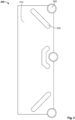
- the substrate 300 comprises the fixation part 322 and the holding part 312. Between the fixation part 322 and the holding part 312 a recess 330 is formed.
- the recess 330 is in the form of long hole or a hole comprising a plurality of long holes.
- a central part is for carrying an electronic component. This part is not or nearly not deformed. This central part comprises the holding part 312.
- the substrate comprises an edge part for being deformed.
- This part comprises the fixation part 322. This part experiences the stress for clamping the substrate in the housing.
- a recess can be arranged abutting to the fixation part for protecting the electronic component from stress caused by deformation of the fixation part.
- the recess can be arranged between the central part and the edge part.
- the pin like fixation means can locally deform the substrate.
- the substrate may comprise an epoxy. Further, as discussed above, the substrate can comprise material having a lower coefficient of thermal expansion than the material comprised in the parts of the housing assembly.
- the assembled part as shown in Fig. 2 comprises a substrate, for example, the substrate shown in Fig. 3 .
- the assembled part comprises a housing and the substrate 300 for holding an electronic component in a chamber.
- the substrate comprises a holding surface 310 and an opposing clamping surface 320.
- the housing enclosing the substrate.
- the housing comprises the base 100 having a protruding holder 110 holding the substrate at a holder part 312 arranged at the holding surface 310, the holder protruding from the base so that the substrate is held at least partially spaced apart from a bottom surface 120 of the base thereby forming a gap between the substrate and the base.
- the hosing comprises the cover 200 having a top surface 220 opposing the bottom surface, the cover being mounted to the base thereby enclosing the substrate.
- the cover comprises the fixation means 210 protruding from the cover in the direction of the bottom surface, the fixation means deforming a fixation part 322 arranged at the fixation surface so that the substrate is clamped in the assembled part.
- the assembled part can comprise a weld 400.
- the weld seals the chamber formed by the housing in which the substrate is clamped from the ingression of media.
- the steps enable assembling a substrate 300 in a housing.
- the substrate is hold in a base 100 of the housing by a protruding holder 110 for forming a gap 130 between the substrate and a bottom surface 120 of the base.
- the substrate is enclosed by moving the cover 200 of the housing to the base 100 thereby assembling the housing. Further, the substrate is deformed by moving the fixation means 210 protruding from the cover in the direction of the bottom surface. As shown in Fig. 2 , the steps of enclosing and deforming the substrate are executed simultaneously by moving a top surface 220 of the cover, the top surface opposing the bottom surface, in the direction of the bottom surface.
- the method may comprise the step of welding the base to the cover for assembling the housing.
- the weld 400 is sealing the interior of the housing.
- an external force is applied to at least one the cover and the base portion for moving the top surface to the bottom surface.
- the molten material which is heated during the welding process, is compressed.
- radiation can be guided trough at least one the cover and the base portion for heating at least one of the base portion and the cover to weld the base station to the cover.
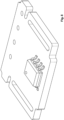
- kits An example of a kit is shown in Fig. 4 .
- the kit comprises a base 100, a substrate 300 with an electronic component 500, and a cover 200.
- the base 100 comprises a rip shaped holder 110. Further, the base may comprise press-fit pins 150 for electrically and/or mechanically connecting the substrate 300 by entering in press-fit opening 350. Further, the base may comprise an opening 160 for receiving a clip 260 of the cover 200. Further, the substrate 300 comprises a recess 330.
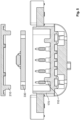
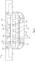
- Fig. 5 shows a sectional view of Fig. 4 .
- the holder 110 is arranged in a central part of the housing, i.e. the holder 110 is arranged spaced apart from a circumferential wall 170 of the base 100.
- the cover 200 comprises a fixation means 210.
- the fixation means 210 is arranged closer to the walls 170 of the housing than the holder.
- the substrate comprises recesses 330, wherein the recesses 330 are arranged between the fixation means 210 and the holder 110.
- Figs. 6 and 9 show that the fixation means 210 may have the shape of a rip.
- Figs. 7 and 8 show that the substrate can have an electronic component 500 that is arranged in a central part to be hold by the holder. Further, an edge part or the substrate is separated from the central part by the recess 330 for protection the electronic component 500 form deformation.
- Fig. 10 is a sectional view of the kit 10 before closing the housing.
- the holding surface 310 and an opposing fixation surface 320 are plane.
- the holding part 312 is hold by the holder of the base.
- the fixation part 322 is still not being deformed by the fixation means of the cover.
- the substrate may have some tolerances to move in the chamber.
- Fig 11 shows a sectional view of the assembled part 1.
- the assembled part 1 is realized by providing the parts of the kit 10, as for example shown in Fig 10 .
- the top surface 220 is moved towards the bottom surface 120.
- the movement is possible because the deformation part 400 is heated thereby melting the deformation part.
- the cover 200 can be moved for a predetermined distance towards the base 100.
- fixation means 210 deforms the substrate 300.
- the fixation part 322 of the substrate deforms.
- the fixation surface 320 is deformed.
- the holding surface 310 deforms.
- REFERENCE NUMERALS Reference Numeral Description 1 assembled part 10 kit 20 space 100 base 110 holder 120 bottom surface 130 gap 150 press-fit pin 160 opening 170 cicumferential wall 200 cover 210 fixation means 220 top surface 260 clip 300 substrate 310 holding surface 312 holding part 320 fixation surface 322 fixation part 330 recess 350 press-fit opening 400 deformable part, weld 500 electronic component
Landscapes
- Engineering & Computer Science (AREA)
- Microelectronics & Electronic Packaging (AREA)
- Casings For Electric Apparatus (AREA)
Abstract
Description
- The invention relates to a housing assembly, an assembled part, and a method for assembling a substrate in a housing.
- A housing assembly is an assembly of parts, e.g. a base and a cover, which together form, when assembled, a housing. A housing is an exterior case or enclosure used to protect an interior mechanism, e.g. a substrate for carrying delicate integrated electrical fittings. Thus, the housing prevents the interior mechanism, e.g. a substrate, from being fouled by outside media, e.g. debris.
- In particular, the interior part, e.g. the substrate may comprise an electronic component used for a sensor. In particular, the sensor application may define requirements for the housing when assembled. In more detail, sensors, e.g. sensors for measuring a temperature, a body's specific force, angular rate, an orientation of the body, or the like, may be used under harsh environmental conditions. For example, a sensor may be used in a gearbox, e.g. of a vehicle or a work tool, or a sensor may be used in a transportation box, e.g. measuring the environmental conditions during shipping.
- For allowing the sensor to be operated, the housing needs to be designed in view of such harsh environmental conditions, in particular the housing may need to protect an interior mechanisms, e.g. the substrate, from external influences. External influences are e.g. structural stress and/or potential physical, thermal, chemical, biological or radiational damages from the surrounding environment, and/or against ingression of media such as fluids or particles.
- In more detail, the harsh environmental conditions may be temporary and/or periodic such that the housing and interior mechanism, e.g. a substrate, may experience thermal variations and or mechanical loads such as vibrations and shocks. Thus, the housing may needs to be designed to be sufficiently robust to be protective in view of the variable harsh environmental conditions. In particular, stress can be caused by change of temperature in the applications by different coefficient of thermal extension (CTE) factors of the components, e.g. the base and the cover may have a different CTE than the interior part, e.g. the substrate. This effect is leading to have a strain release in all directions of the interconnection areas.
- Further, various fabrications techniques are known to manufacture a housing. However, the technics may have drawbacks in view of enclosing an interior mechanism, e.g. a substrate. For example, ultrasonic welding can stress the overall assembly in a critical way, in particular by destroying the electrical components hold by the substrate. Clipping a cover to a base may leading in complex cover geometries in view of additional necessary sealing element.
- Further, a housing for an interior mechanism, e.g. a substrate, may require a plurality of mounting steps, additional components, and/or providing during the mounting additional materials.
- At least one of objects discussed above is solved by the independent claims. Advantageous embodiments are solved by the dependent claims.
- The present disclosure proposes a housing assembly comprising a base and a cover. The base holds a substrate, e.g. a printed circuit assembly (PCB). Further, the cover comprises a fixation means protruding from the cover for deforming the substrate. Thus, when assembling the cover to the base, two process steps are performed at the same time, namely the cover is mounted on the base forming the assembled housing enclosing the substrate. At the same time, the fixation means deforms the substrate, and thus, fixes the substrate in the enclosed housing.
- Thus, the housing assembly allows minimizing the cost-to-function by a minimum of components/materials and process-steps.
- In more detail, the following description relates to a housing assembly for enclosing and clamping a substrate in a chamber.
- As used herein, a housing assembly is an assembly of parts, the parts comprising a base and a cover, which together form, when assembled, a housing. The housing assembly protects a substrate by mounting the base to the cover. The housing assembly encloses the substrate. Enclosing means that the assembled parts build walls around the substrate. In other words, the assembled parts form the chamber wherein the substrate is placed. Such an arrangement allows preventing the substrate from being fouled by outside media.
- As used herein, a substrate describes the base material on which processing is conducted. In particular, the substrate is used for carrying an electronic component. In more detail, the substrate is used to form a printed circuit board (PCB) or a printed circuit board assembly (PCBa). A typical substrate might be rigid such as an epoxy or glass, onto which a coating might be deposited.
- As used herein, clamping the substrate in the chamber means that the substrate is hold fastened or fixed in the camber. In other words, the substrate cannot move in the chamber when clamped. Such an arrangement prevents that the substrate moves relative to the housing when the housing experiences thermal variations and/or mechanical loads such as vibrations and shocks.
- The housing assembly comprises the base having a protruding holder for holding the substrate in the chamber. In particular, the base being an accommodation such as a recessed part having a bottom wall and side walls protruding from the bottom wall for receiving and partly enclosing the substrate.
- Further, the holder is for example a plateau, a pin or a similar structure protruding from the base, e.g. from the bottom or the side wall. Such an arrangement enables that the substrate is held at least partially spaced apart from a bottom surface of the base. In other words, the holder protrudes in the chamber.
- According to an example, the base forms the recessed part with the bottom wall forming the bottom surface and side walls. The bottom surface being for example a generally plane surface and the holder, e.g. the plateau shaped holder or a holder formed by on ore more pins, protrudes in the direction of the surrounding wall from the bottom surface. Thus, the substrate rests on the holder and a gap is formed between the substrate and the bottom surface. In other words, the substrate does not rest on the bottom surface but is held spaced apart from the bottom surface by the holder. Alternatively, the holder may protrude from the side wall of the base which allows also forming a gap between the substrate and the bottom surface.
- Further, the housing assembly comprises a cover having a top surface opposing the bottom surface. According to an example, the cover may be a plate for being mounted to the side wall of the base. Alternatively, the cover may comprises a cover wall and a cover side wall protruding from the cover side wall, the cover side wall for being mounted to the side wall of the base.
- In addition, to assemble the housing, i.e. enclosing the substrate, the top surface is moved towards the bottom surface. To close the housing, the cover may for example be welded, screwed, welded or clipped to the base. In particular, each of the mounting technics comprises a translation of the top surface in the direction of the bottom surface thereby closing a gap between the cover and the base, and thus, enclosing the substrate.
- Further, the cover comprises a fixation means, e.g. a pin such as a columnar structure, protruding from the cover in the direction of the bottom surface. The fixation means deforms the substrate when the top surface is moved towards the bottom surface, i.e. when the cover encloses the substrate. In other words, the fixation means is arranged on the cover so that it protrudes in the chamber. According to an example, in case the base being a recessed part having a bottom wall and side walls, the fixation means protrudes in the space that is enclosed by the base.
- The fixation means enables that within one process step, namely moving the cover towards the base, two process steps are performed, namely enclosing the substrate and at the same time deforming the substrate so that the substrate is clamped between the fixation means and the holder. In particular, the gap formed between the base and the bottom surface allows that the substrate elastically deforms. In other words, the fixation means acts as a spring bias clamping the substrate in the chamber.
- In other words, a spring-load is applied by a partly deformation of a decoupled section of the substrate, e.g. the PCBa or the PCB, by a geometry which is realized by the cover of the housing.
- The pressing features and the deformation for deforming the substrate, e.g. the PCB, over a fixation part, which is also referred to as deformation area or spring loaded area, can be calculated according to the IPC standards in order to keep the integrity of all components.
- According to an aspect, the housing assembly comprises a deformable part for sealing the assembled housing. As used herein, the deformable part enables that the deformable part undergoes a plastic or elastic deformation.
- For example, by welding the cover to the base, the deformable part may be the part that transforms to the weld that undergoes a plastic, i.e. non-reversible deformation. Alternatively, by screwing or clipping the cover to the base, the deformable part may be a sealing element, e.g. a sealing ring, which elastically deforms when assembling housing.
- Further, the deformable part is for being compressed when moving the top surface towards the bottom surface. In particular, the deformable part being compressed in the direction of moving the top surface towards the bottom surface.
- According to an example, in particular when using a welding process, at least one of the base or the cover comprises the deformable part, the deformable part being arranged at the edge of the base or the cover. Thus, an edge of the cover or the base is deformed by the welding process.
- Alternatively, the deformable part can be an additional part, e.g. a sealing element, which is arranged between the base and the cover. Such a sealing element may be used when for example clipping or screwing is used for mounting the cover to the base.
- The deformable part enables that within one process step, namely moving the cover towards the base, three process steps are performed, namely enclosing the substrate, deforming the substrate so that the substrate is clamped between the fixation means and the holder, and at the same time sealing the housing. In particular, the deformable part defines by its construction by how much the top surface is moving towards the bottom surface. This additionally defines by which amount the substrate elastically deforms. In other words, the deformation part acts as a measure for defining the spring bias applied to the substrate.
- According to an aspect, the deformable part comprises a thermoplastic material for melting when heated. Thus, the assembled housing comprises a weld or fusion zone for sealing the housing.
- As used herein, a thermoplastic, or thermosoft plastic, is a plastic polymer material that becomes pliable or moldable at a certain elevated temperature and solidifies upon cooling. The polymer chains associate by intermolecular forces, which weaken rapidly with increased temperature, yielding a viscous liquid. In this state, thermoplastics may be reshaped and are typically used to produce parts by various polymer processing techniques such as injection molding, compression molding, calendaring, and extrusion.
- As used in the present disclosure, welding is a fabrication process that joins materials, usually metals or thermoplastics, by using high heat to melt the parts together and allowing them to cool, causing fusion. Welding is distinct from lower temperature techniques such as brazing and soldering, which do not melt the base metal. The fusion zone allows sealing of the chamber in the housing. In particular, the fusion zone is stable even under harsh environmental conditions.
- Thus, providing a deformable part comprising a thermoplastic enables that the number of parts is reduced. In particular, at least one of the cover and the base may comprise the thermoplastic material thereby additionally being adapted for welding.
- In addition, the process step of moving the cover towards the base enables a particularly strong welded connection. In particular, during the welding process, pressure is applied to the parts. Thus, a particular strong weld it formed.
- According to a further aspect, one of the cover and the base is transparent for guiding light to the deformable part for joining the base to the cover by laser welding.
- As used herein, transparent means that a part of the radiation emitted by a radiation source such as a laser is guided through the cover or the base to the deformable part. For example, down to 10 % of the radiation emitted by radiation source may be guided through the cover or the base which, which thus is transparent. The material and the thickness of the cover or the base may be chosen so that the cover or the base becomes transparent for a radiation source having for example a wavelength larger equal 630 nm and less equal 1100 nm.
- This transparent part allows for radiation welding such as laser or electron beam welding. Laser welding is a welding technique used to join pieces of metal or thermoplastics by the use of a laser. The beam provides a concentrated radian energy source, allowing for narrow, deep welds and high welding rates. The process is frequently used in high volume applications using automation, as in the automotive industry.
- Equipment for e.g. thermoplastic Laser-welding using e.g. red or infrared light, which covers wavelength larger equal 630 nm and less equal 1100 nm, e.g. A = 980 nm wave length. Such lasers are well established in the market and thus is a readily available technology that is globally available.
- This enables for using a welding appliance, which provides two functions, namely heating the deformable part to weld the cover to the base. At the same time, the welding appliance can comprise means for pressing the cover to the base. Typically, welding appliance have implemented both functions, and thus, cost-to-function is minimized.
- In other words, during operation of the radiation source, e.g. the laser, the cover can be moved into direction of the base. This process is also referred to as setting. Thus, the housing closes tight and in a mechanically robust manner.
- According to a further aspect, the fixation means protrudes from the top surface. For example, the fixation means protrudes in the direction of the normal of the top surface, which for example is a flat surface. Such an arrangement allows a particularly stable configuration.
- According to a further aspect, the holder protrudes from the bottom surface. For example, the holder protrudes in the direction of the normal of the bottom surface, which for example is a flat surface. Such an arrangement allows a particularly stable configuration.
- Further, the following description relates to a kit for assembled part, the kit comprising a substrate for carrying an electronic component and a housing assembly as describe above for enclosing the substrate.
- The substrate, which has been described above, comprises a holding surface and an opposing fixation surface. In particular, the substrate is a flat part such as PCB. For example, the substrate comprises an insulating layer for affix electronic components in designated locations. Further, the substrate can comprise a contacting layer for provide reliable electrical connections (and also reliable open circuits) between the component's terminals in a controlled manner.
- Further, the holding surface comprises a holding part for being hold by the holder of the base. In particular, the holding part is part of the insulating layer.
- Further, the fixation surface comprising a fixation part for being deformed by the fixation means of the cover for fixing the substrate in the chamber. In particular, the fixation part is a part of the insulating layer.
- Thus, the substrate allows for being clamped in the housing. As described above, the pressing features and the deformation for deforming the substrate, e.g. the PCB, over the fixation part can be calculated according to the IPC standards and is defined by the geometry of the housing.
- According to an aspect, the substrate comprises an epoxy.
- As used herein, epoxy is the family of basic components or cured end products of epoxy resins. In particular, an insulating layer of the substrate comprises or consists of epoxy. The insulating layer, which is used for carrying electronic components, has thus a low tendency for creeping. As used herein, creep (sometimes called cold flow) is the tendency of a solid material to move slowly or deform permanently under the influence of persistent mechanical stresses. It can occur as a result of long-term exposure to high levels of stress that are still below the yield strength of the material. Creep is more severe in materials that are subjected to heat for long periods and generally increases as they near their melting point.
- In particular, the substrate, e.g. a PCBa or PCB, comprising epoxy has the character of having a low or no creeping effect, which has for example proven by interconnections used for substrates comprising epoxy like press-fit connections.
- Thus, using a substrate comprising an epoxy enables a particularly long-term stability of the parts.
- In particular, the tendency of creeping of the substrate is lower than the tendency of creeping of the housing element, in particular in the case of the housing comprising thermoplastic materials.
- According to an aspect, the substrate comprises a recess. As used herein, a recess is a part of the substrate that is thinner, for example a through hole, than the rest of the substrate, forming a space.
- Further, the recess being arranged abutting to the fixation part. As used herein, abutting means that the recess is next to the fixation part, in particular, to have one side touching the side of the fixation portion. In other words, an electric component free area is formed between the fixation part and the recess, in particular the electric component free area only comprises isolating material.
- Thus, the electronic component is protected from stress caused by deformation of the fixation part of the substrate.
- According to an aspect, the substrate comprises material having a lower coefficient of thermal expansion (CTE) than the material comprised in the parts of the housing assembly.
- As generally known, thermal expansion decreases with increasing bond energy, which also has an effect on the melting point of solids, so, high melting point materials are more likely to have lower thermal expansion. In particular, for enabling that the housing parts are joint by a welding process, the housing parts comprise a material such as a thermoplastic, which melts, for example at a temperature of about 200° C to 400° C. On the other hands, the substrate is in particular a thermoset such as an epoxy with has particularly strong bonds. Cured thermosets usually do not melt and have compared to a housing comprising thermoplastics for welding a lower thermal expansion.
- The above described arrangement allows to clamp the substrate by the housing even in a case of materials having a different CTE. In particular, upon heating, the housing parts expand. In view of the fixation means and the holder protruding from the top surface and the bottom surface respectively, the complete housing experiences the thermal expansion. In view of this geometric configuration, the fixation of the substrate does not change upon temperature changes.
- Further, the following description relates to an assembled part comprising a housing and a substrate for holding an electronic component in a chamber. For the description of the housing, the substrate, the electronic component, and the chamber is referred to the above description.
- Further, the substrate of the assembled part comprises a holding surface and an opposing clamping surface. For the description of the holding surface and an opposing clamping surface is referred to the above description.
- Further, the housing enclosing the substrate comprises a base and cover. For the description of the base and the cover is referred to the above description.
- The base has a protruding holder holding the substrate at a holding part arranged at the holding surface, the holder protruding from the base so that the substrate is held at least partially spaced apart from a bottom surface of the base thereby forming a gap between the substrate and the base. For the description of the holder, the holding part, the bottom surface, and the gap is referred to the above description. Notably, the holding surface is at least partly facing the bottom surface thereby forming the gap.
- The cover has a top surface opposing the bottom surface, the cover being mounted to the base thereby enclosing the substrate. For the description of the top surface is referred to the above description.
- Further, the cover comprises a fixation means protruding from the cover in the direction of the bottom surface, the fixation means deforming a fixation part arranged at the fixation surface so that the substrate is clamped in the assembled part. For the description of the fixation means and the fixation part is referred to the above description.
- In particular, the assembled part can be realized using the kit described above.
- According to an aspect, the housing of the assembled part comprises a weld, the weld sealing the chamber formed by the housing in which the substrate is clamped from ingression of media. For a description of the weld is referred to the above description. In particular, the weld comprises material of at least one of the cover and the base.
- According to a further aspect, the assembled part comprises a deformable part for sealing the assembled housing, the deformable part being compressed. For a description of the deformable part is referred to the above description. In particular, the deformable part comprises a thermoplastic material for melting when heated.
- According to a further aspect, at least one of the cover and the base of the assembled part is transparent for guiding light to the deformable part for joining the base to the cover by radiation welding. For a description of the transparent parts is referred to the above description.
- According to a further aspect, the fixation means protrudes from the top surface and/or the holder protrudes from the bottom surface.
- According to a further aspect, the substrate of the assembled part comprises a recess, the recess being arranged abutting to the fixation part for protecting the electronic component from stress caused by deformation of the fixation part. For a description of the recess is referred to the above description.
- Further, the following description relates to a method for assembling a substrate in a housing, the method comprising the steps of:
- holding a substrate in a base of the housing by a protruding holder for forming a gap between the substrate and a bottom surface of the base;
- enclosing the substrate being hold in the base by moving a cover of the housing to the base thereby assembling the housing;
- deforming the substrate being hold in the base by moving a fixation means protruding from the cover in the direction of the bottom surface;
- wherein the steps of enclosing and deforming the substrate are executed simultaneously by moving a top surface of the cover, the top surface opposing the bottom surface, in the direction of the bottom surface.
- In particular, the method relates to assembling the kit described above. For further details of the method steps is referred to the above.
- As used herein, simultaneously means that the process steps are performed at the same time and are caused by the same process step, namely moving the top surface of the cover in the direction of the bottom surface.
- According to an aspect, the method comprises welding the base to the cover for assembling the housing. For the description of the process of welding is referred to the above description. In particular, the step of wherein the steps of welding the housing, enclosing the substrate, and deforming the substrate are executed simultaneously.
- According to an aspect, the method comprises applying external force to at least one the cover and the base portion for moving the top surface to the bottom surface. As used herein, applying external force means that the top surface is actively moved to the bottom surface. For example, as described above, during operation of a radiation source, e.g. a laser, the cover can be moved into direction of the base by applying external force. This process is also referred to as setting. Thus, the housing closes tight and in a mechanically robust manner.
- According to an aspect, the method comprises guiding radiation trough at least one the cover and the base portion for welding the base portion to the cover. As used herein, guiding radiation trough a part means that the part is transparent. For the description of the transparent part is referred to the above description. Such a configuration enables that a welding appliance can be used, which provides two functions, namely heating the deformable part to weld the cover to the base. At the same time, the welding appliance can comprise means for pressing the cover to the base. Typically, welding appliance have implemented both functions, and thus, cost-to-function is minimized.
- The invention will now be described in greater detail and in an exemplary manner using advantageous embodiments and with reference to the drawings. The described embodiments are only possible configurations in which, however, the individual features as described above can be provided independently of one another or can be omitted.
- The accompanying drawings are incorporated into the specification and form a part of the specification to illustrate several embodiments of the present invention. These drawings, together with the description serve to explain the principles of the invention. The drawings are merely for the purpose of illustrating the preferred and alternative examples of how the invention can be made and used, and are not to be construed as limiting the invention to only the illustrated and described embodiments. Furthermore, several aspects of the embodiments may form-individually or in different combinations-solutions according to the present invention. The following described embodiments thus can be considered either alone or in an arbitrary combination thereof. The described embodiments are merely possible configurations and it must be borne in mind that the individual features as described above can be provided independently of one another or can be omitted altogether while implementing this invention. Further features and advantages will become apparent from the following more particular description of the various embodiments of the invention, as illustrated in the accompanying drawings, in which like references refer to like elements, and wherein:
- FIG. 1
- is a schematic of a kit according to one aspect before assembling;
- FIG. 2
- is a schematic of the kit of
Fig. 1 after assembling; - FIG. 3
- is a schematic of a detail of
Fig. 1 showing a substrate according to one aspect; - FIG. 4
- is an exploded view of a kit according to an example;
- FIG. 5
- is a sectional view of
Fig. 4 ; - FIG. 6
- is an exploded view of a substrate and a cover of
Fig. 4 ; - FIG. 7
- is a top view of the substrate of
Fig. 4 ; - FIG. 8
- is a further view of the substrate of
Fig. 4 ; - FIG. 9
- is a view of the cover of
Fig. 4 ; - FIG. 10
- is a sectional view of the kit of
Fig. 4 before assembling; and - FIG. 11
- is a sectional view of the kit of
Fig. 4 after assembling. - The present invention will now be explained in more detail with reference to the Figures. Referring to
Fig. 1 , a schematic of akit 10 according to one aspect is described. - In particular, the
kit 10 for an assembled part comprises asubstrate 300 for carrying an electronic component. Further, thekit 10 comprises a housing assembly for enclosing the substrate. - The housing assembly comprises a
base 100. Thebase 100 has a protrudingholder 110 for holding the substrate in the chamber, the holder protruding from the base so that the substrate is held at least partially spaced apart from abottom surface 120 of the base thereby forming agap 130. - For example, as shown in
Fig. 1 , thebase 100 is a recessed part with bottom wall and a side wall protruding from the bottom wall. Theholder 110 is a plateau arranged in a central part of the bottom wall. In other words, the gap is arranged at a circumferential part of the substrate. This enables that the later to be described fixation means 210 can clamp a circumferential part of thesubstrate 300. - Alternatively, the holder may be a pin, i.e. a columnar structure, a rip, or the like. Further, the base may only a plate without side walls. Further, the holder may be arranged at an edge part base.
- The
substrate 300 may be mounted to the holder, e.g. by using press fit pins, gluing, clipping, screwing the substrate to the bottom wall. Alternatively, the substrate may be lay on the holder without being fixed to the holder. - Further, the
cover 200 has atop surface 220. Thetop surface 220 opposes thebottom surface 120. In other words, thetop surface 220 and thebottom surface 120 are facing the chamber of the housing. - The
cover 200 is for enclosing thesubstrate 300 by moving the top surface towards the bottom surface. In particular,Fig. 1 shows the parts before assembling. Aspace 20 can be identified between thecover 200 and thebase 100. - Further, the cover comprises the fixation means 210 protruding from the
cover 200 in the direction of thebottom surface 120. - As shown in
Fig. 2 , showing an assembledpart 1 formed by assembling thekit 10 ofFig. 1 , the fixation means 210 deforms thesubstrate 300. Thus, the fixation means 210 clamps the substrate is in the assembled housing when the cover encloses the substrate. - For example, as shown in
Figs. 1 and 2 , thecover 100 is a recessed part with top wall and a side wall protruding from the top wall. The fixation means 210 is a pin arranged in a circumferential part of the top wall. Thus, the fixation means can clamp a circumferential part of the substrate. - Alternatively, the fixation means may be a rip, a plateau, or the like. Further, the cover may only be a plate without side walls. Further, the fixation means may be arranged at a central part of the cover.
- As shown in
Figs. 1 and 2 , the substrate comprises a holdingsurface 310 and an opposingfixation surface 320. In other words, the substrate is a flat body. As used herein, a flat body is geometric body in the form of whose lateral dimension, e.g. a radius of a cylinder, is many times, e.g. 10 times, greater than its thickness. - Further, the holding
surface 120 comprises a holding part for being hold by theholder 110 of the base. For example, as shown inFigs. 1 and 2 , the holding part is a central part of the substrate. - Further, the
fixation surface 320 comprising a fixation part for being deformed by the fixation means 210 of the cover for fixing the substrate in the chamber. In particular, as shown inFig. 1 , the fixation means 210 is not in contact with the fixation part, and thus, the substrate is not deformed. - Further, as shown in
Fig. 2 , the fixation means 210 is in contact withsubstrate 300 and the substrate is deformed. Thus, thesubstrate 300 is clamped in the housing. - Further, the housing assembly may comprise a deformable part for sealing the assembled housing. For example, the deformable part may be a sealing arranged in the
space 20. Additionally or alternatively, the deformable part may be an edge part of the side wall of the base abutting to thespace 20. Additionally or alternatively, the deformable part may be a part of the cover abutting to thespace 20. - The deformable part is adapted for being compressed when moving the top surface towards the bottom surface. In other words, when the parts of
Fig. 1 are assembled, as shown inFig. 2 , thedeformable part 400 is compressed and arranged at the connection of thebase 100 and thecover 200. - Further, the deformable part may comprise a thermoplastic material for melting when heated. In particular, the deformable can be for example an edge part of the side wall of the base abutting to the
space 20 or a part of the cover abutting to thespace 20. Thus the cover can be welded to the base without the need of providing a further material, e.g. an adhesive. In other words, a part of at least one of the cover and the base is melting during heating, thereby deforming. - Further, at least one of the
cover 200 and the base 100 can be made from a transparent material for guiding light to the deformable part for joining the base to the cover by radiation welding. For example, inFig. 1 thecover 200 is made from a transparent material. Thus, theweld 400 can be generated. Further, theweld 400 can be protected by the side wall of thecover 200 form external influences. - Further, as shown in
Figs. 1 and 2 , the fixation means 210 protrudes from thetop surface 220. Further,holder 110 protrudes from thebottom surface 120. Alternatively, according to a not shown solution, the holder may for example protrude from a side wall of the base. - Further, as shown in
Figs. 1 and 2 , the fixation part is an edge part of the substrate. In particular, the fixation part surrounds the central part. Notably, the fixation part and the holding part are not overlapping in a dimension having as a normal the axis of moving the top surface towards the bottom surface. This enables the deformation of the substrate. For the same reasons, the holder and the fixation means are arranged shifted in the housing so that fixation means moved in the direction of the gap when the top surface moves towards the bottom surface. - Further details of the substrate are shown in
Fig. 3 . In particular, thesubstrate 300 comprises thefixation part 322 and the holdingpart 312. Between thefixation part 322 and the holding part 312 arecess 330 is formed. In particular, therecess 330 is in the form of long hole or a hole comprising a plurality of long holes. - Thus, the substrate is divided in sections having different functionality. A central part is for carrying an electronic component. This part is not or nearly not deformed. This central part comprises the holding
part 312. - Further, the substrate comprises an edge part for being deformed. This part comprises the
fixation part 322. This part experiences the stress for clamping the substrate in the housing. - Further, a recess can be arranged abutting to the fixation part for protecting the electronic component from stress caused by deformation of the fixation part. In particular, the recess can be arranged between the central part and the edge part. For example, the pin like fixation means can locally deform the substrate. Providing
recesses 330 enables reducing the stress effects thereby allowing to increase the central part which can carry the electronic components. - Further, as discussed above, the substrate may comprise an epoxy. Further, as discussed above, the substrate can comprise material having a lower coefficient of thermal expansion than the material comprised in the parts of the housing assembly.
- The assembled part as shown in
Fig. 2 comprises a substrate, for example, the substrate shown inFig. 3 . In particular, the assembled part comprises a housing and thesubstrate 300 for holding an electronic component in a chamber. The substrate comprises a holdingsurface 310 and an opposingclamping surface 320. The housing enclosing the substrate. The housing comprises the base 100 having a protrudingholder 110 holding the substrate at aholder part 312 arranged at the holdingsurface 310, the holder protruding from the base so that the substrate is held at least partially spaced apart from abottom surface 120 of the base thereby forming a gap between the substrate and the base. Further, the hosing comprises thecover 200 having atop surface 220 opposing the bottom surface, the cover being mounted to the base thereby enclosing the substrate. Further, the cover comprises the fixation means 210 protruding from the cover in the direction of the bottom surface, the fixation means deforming afixation part 322 arranged at the fixation surface so that the substrate is clamped in the assembled part. - In particular, the assembled part can comprise a
weld 400. The weld seals the chamber formed by the housing in which the substrate is clamped from the ingression of media. - For assembling the parts as shown in
Fig. 1 , the following method may be performed. In particular, the steps enable assembling asubstrate 300 in a housing. As a first step, which is shown inFig. 1 , the substrate is hold in abase 100 of the housing by a protrudingholder 110 for forming agap 130 between the substrate and abottom surface 120 of the base. - Further, as shown in
Fig. 2 , the substrate is enclosed by moving thecover 200 of the housing to the base 100 thereby assembling the housing. Further, the substrate is deformed by moving the fixation means 210 protruding from the cover in the direction of the bottom surface. As shown inFig. 2 , the steps of enclosing and deforming the substrate are executed simultaneously by moving atop surface 220 of the cover, the top surface opposing the bottom surface, in the direction of the bottom surface. - Further, the method may comprise the step of welding the base to the cover for assembling the housing. Thus, the
weld 400 is sealing the interior of the housing. In particular, an external force is applied to at least one the cover and the base portion for moving the top surface to the bottom surface. Thus, the molten material, which is heated during the welding process, is compressed. Further, for enabling the welding step, radiation can be guided trough at least one the cover and the base portion for heating at least one of the base portion and the cover to weld the base station to the cover. - An example of a kit is shown in
Fig. 4 . In particular, the kit comprises abase 100, asubstrate 300 with anelectronic component 500, and acover 200. - The
base 100 comprises a rip shapedholder 110. Further, the base may comprise press-fit pins 150 for electrically and/or mechanically connecting thesubstrate 300 by entering in press-fit opening 350. Further, the base may comprise anopening 160 for receiving aclip 260 of thecover 200. Further, thesubstrate 300 comprises arecess 330. - Further,
Fig. 5 shows a sectional view ofFig. 4 . In particular, theholder 110 is arranged in a central part of the housing, i.e. theholder 110 is arranged spaced apart from acircumferential wall 170 of thebase 100. Thecover 200 comprises a fixation means 210. The fixation means 210 is arranged closer to thewalls 170 of the housing than the holder. Finally, the substrate comprisesrecesses 330, wherein therecesses 330 are arranged between the fixation means 210 and theholder 110. - Further,
Figs. 6 and9 show that the fixation means 210 may have the shape of a rip. Further,Figs. 7 and8 show that the substrate can have anelectronic component 500 that is arranged in a central part to be hold by the holder. Further, an edge part or the substrate is separated from the central part by therecess 330 for protection theelectronic component 500 form deformation. - In particular,
Fig. 10 is a sectional view of thekit 10 before closing the housing. In particular, the holdingsurface 310 and an opposingfixation surface 320 are plane. In particular, the holdingpart 312 is hold by the holder of the base. Thefixation part 322 is still not being deformed by the fixation means of the cover. Thus, the substrate may have some tolerances to move in the chamber. - Further,
Fig 11 shows a sectional view of the assembledpart 1. In particular, the assembledpart 1 is realized by providing the parts of thekit 10, as for example shown inFig 10 .Thetop surface 220 is moved towards thebottom surface 120. - For example, the movement is possible because the
deformation part 400 is heated thereby melting the deformation part. By applying a force across the cover and the base, thecover 200 can be moved for a predetermined distance towards thebase 100. - This movement causes that the fixation means 210 deforms the
substrate 300. In particular, in view of theholder 110, thefixation part 322 of the substrate deforms. Thus, thefixation surface 320 is deformed. Similarly, the holdingsurface 310 deforms.REFERENCE NUMERALS Reference Numeral Description 1 assembled part 10 kit 20 space 100 base 110 holder 120 bottom surface 130 gap 150 press- fit pin 160 opening 170 cicumferential wall 200 cover 210 fixation means 220 top surface 260 clip 300 substrate 310 holding surface 312 holding part 320 fixation surface 322 fixation part 330 recess 350 press- fit opening 400 deformable part, weld 500 electronic component
Claims (15)
- Housing assembly for enclosing and clamping a substrate (300) in a chamber, the housing assembly comprisinga base (100) having a protruding holder (110) for holding the substrate in the chamber, the holder protruding from the base so that the substrate is held at least partially spaced apart from a bottom surface of the base thereby forming a gap (130);a cover (200) having a top surface (220) opposing the bottom surface, the cover for enclosing the substrate by moving the top surface towards the bottom surface;wherein the cover comprises a fixation means (210) protruding from the cover in the direction of the bottom surface, the fixation means for deforming the substrate so that the substrate is clamped in the assembled housing when the cover encloses the substrate.
- Housing assembly according to claim 1, further comprising a deformable part (400) for sealing the assembled housing, the deformable part for being compressed when moving the top surface towards the bottom surface.
- Housing assembly according to claim 2, wherein the deformable part comprises a thermoplastic material for melting when heated.
- Housing assembly according to any of claims 2 to 3, wherein at least one of the cover and the base is transparent for guiding light to the deformable part for joining the base to the cover by radiation welding.
- Housing assembly according to any of claims 1 to 4, wherein the fixation means protrudes from the top surface and/or the holder protrudes from the bottom surface.
- Kit for an assembled part (1), the kit (10) comprising a substrate (300) for carrying an electronic component (500) and a housing assembly according to any of claims 1 to 5 for enclosing the substrate,
the substrate comprising a holding surface (310) and an opposing fixation surface (320), wherein the holding surface comprises a holding part (312) for being hold by the holder of the base and the fixation surface comprising a fixation part (322) for being deformed by the fixation means of the cover for fixing the substrate in the chamber. - Kit according to claim 6, wherein the substrate comprises an epoxy.
- Kit according to claims 6 or 7, wherein the substrate comprises a recess (330), the recess being arranged abutting to the fixation part for protecting the electronic component from stress caused by deformation of the fixation part.
- Kit according to claims 6 to 8, wherein the substrate comprises material having a lower coefficient of thermal expansion than the material comprised in the parts of the housing assembly.
- Assembled part comprising a housing and a substrate (300) for holding an electronic component (500) in a chamber,
the substrate comprises a holding surface (310) and an opposing clamping surface (320), the housing enclosing the substrate comprises:a base (100) having a protruding holder (110) holding the substrate at a holder part (312) arranged at the holding surface (310), the holder protruding from the base so that the substrate is held at least partially spaced apart from a bottom surface (120) of the base thereby forming a gap between the substrate and the base;a cover (200) having a top surface (220) opposing the bottom surface, the cover being mounted to the base thereby enclosing the substrate; andwherein the cover comprises a fixation means (210) protruding from the cover in the direction of the bottom surface, the fixation means deforming a fixation part (322) arranged at the fixation surface so that the substrate is clamped in the assembled part (1). - Assembled part according to claim 10, wherein the housing comprises a weld (400), the weld sealing the chamber formed by the housing in which the substrate is clamped from the ingression of media.
- Method for assembling a substrate in a housing, the method comprising the steps of:holding a substrate in a base of the housing by a protruding holder for forming a gap between the substrate and a bottom surface of the base;enclosing the substrate being hold in the base by moving a cover of the housing to the base thereby assembling the housing;deforming the substrate being hold in the base by moving a fixation means protruding from the cover in the direction of the bottom surface;wherein the steps of enclosing and deforming the substrate are executed simultaneously by moving a top surface of the cover, the top surface opposing the bottom surface, in the direction of the bottom surface.
- Method for assembling the substrate in the housing according to claim 12, further comprising welding the base to the cover for assembling the housing.
- Method for assembling the substrate in the housing according to any of claims 12 to 13, further comprising applying external force to at least one the cover and the base for moving the top surface to the bottom surface.
- Method for assembling the substrate in the housing according to any of claims 13 to 14, further comprising guiding radiation trough at least one the cover and the base portion for welding the base portion to the cover.
Priority Applications (1)
| Application Number | Priority Date | Filing Date | Title |
|---|---|---|---|
| EP22177310.4A EP4287793B1 (en) | 2022-06-03 | 2022-06-03 | Housing assembly, assembled part, and method for assembling a substrate in a housing |
Applications Claiming Priority (1)
| Application Number | Priority Date | Filing Date | Title |
|---|---|---|---|
| EP22177310.4A EP4287793B1 (en) | 2022-06-03 | 2022-06-03 | Housing assembly, assembled part, and method for assembling a substrate in a housing |
Publications (2)
| Publication Number | Publication Date |
|---|---|
| EP4287793A1 true EP4287793A1 (en) | 2023-12-06 |
| EP4287793B1 EP4287793B1 (en) | 2026-08-19 |
Family
ID=81941116
Family Applications (1)
| Application Number | Title | Priority Date | Filing Date |
|---|---|---|---|
| EP22177310.4A Active EP4287793B1 (en) | 2022-06-03 | 2022-06-03 | Housing assembly, assembled part, and method for assembling a substrate in a housing |
Country Status (1)
| Country | Link |
|---|---|
| EP (1) | EP4287793B1 (en) |
Citations (7)
| Publication number | Priority date | Publication date | Assignee | Title |
|---|---|---|---|---|
| US20060044768A1 (en) * | 2004-08-26 | 2006-03-02 | Denso Corporation | Electronic apparatus including circuit board chassis |
| US20110168441A1 (en) * | 2008-07-17 | 2011-07-14 | Andre Lischeck | Electrical circuitry |
| DE102015117223A1 (en) * | 2015-10-09 | 2017-04-13 | Visteon Global Technologies Inc. | Electronic arrangement |
| CN112839455A (en) * | 2019-11-22 | 2021-05-25 | 新电元工业株式会社 | Electronic device |
| DE102020211730B3 (en) * | 2020-09-14 | 2021-08-26 | Continental Automotive Gmbh | Housing for an electronic circuit arranged on a printed circuit board |
| KR20220000090A (en) * | 2020-06-25 | 2022-01-03 | 현대모비스 주식회사 | Air bag contrl unit |
| US20220030737A1 (en) * | 2018-10-18 | 2022-01-27 | Mitsubishi Electric Corporation | Board housing case |
-
2022
- 2022-06-03 EP EP22177310.4A patent/EP4287793B1/en active Active
Patent Citations (7)
| Publication number | Priority date | Publication date | Assignee | Title |
|---|---|---|---|---|
| US20060044768A1 (en) * | 2004-08-26 | 2006-03-02 | Denso Corporation | Electronic apparatus including circuit board chassis |
| US20110168441A1 (en) * | 2008-07-17 | 2011-07-14 | Andre Lischeck | Electrical circuitry |
| DE102015117223A1 (en) * | 2015-10-09 | 2017-04-13 | Visteon Global Technologies Inc. | Electronic arrangement |
| US20220030737A1 (en) * | 2018-10-18 | 2022-01-27 | Mitsubishi Electric Corporation | Board housing case |
| CN112839455A (en) * | 2019-11-22 | 2021-05-25 | 新电元工业株式会社 | Electronic device |
| KR20220000090A (en) * | 2020-06-25 | 2022-01-03 | 현대모비스 주식회사 | Air bag contrl unit |
| DE102020211730B3 (en) * | 2020-09-14 | 2021-08-26 | Continental Automotive Gmbh | Housing for an electronic circuit arranged on a printed circuit board |
Also Published As
| Publication number | Publication date |
|---|---|
| EP4287793B1 (en) | 2026-08-19 |
Similar Documents
| Publication | Publication Date | Title |
|---|---|---|
| US9030835B2 (en) | Method for welding a plastic housing | |
| JP5675933B2 (en) | Control device housing | |
| CN101406039B (en) | Method for assembling a camera module, and camera module | |
| CN104685975B (en) | Components for electronic modules‑housing | |
| CN108141979B (en) | Electronic control device and manufacturing method of electronic control device | |
| JP4847198B2 (en) | Method for constructing electronic circuit housing | |
| EP0522687B1 (en) | Hermetic Connector | |
| US6552911B1 (en) | Electrical device | |
| KR100995237B1 (en) | Camera device with image sensor sealed from environmental impact | |
| US20100078115A1 (en) | Use of a Device for Torsional Ultrasonic Welding | |
| US20050201069A1 (en) | Electronic device | |
| EP1898684A1 (en) | Sealed electronic component | |
| KR20140098069A (en) | Electronic module for a control unit | |
| CN102331322B (en) | Pressure sensor chip | |
| WO1993020467A1 (en) | Optical module and manufacture thereof | |
| CN101738288B (en) | Sensor assembly and the method for the manufacture of sensor assembly | |
| KR101240408B1 (en) | Method of assembling housing of photoelectric sensor and photoelectric sensor | |
| KR20070089704A (en) | Control module | |
| US5986208A (en) | Waveguide window assembly and microwave electronics package | |
| CN1660559B (en) | Laser Welding of Resin Parts Using Ridges to Enhance Welding Strength | |
| WO2019012898A1 (en) | Electronic control device and method for manufacturing electronic control device | |
| US7135768B2 (en) | Hermetic seal | |
| JP2002529789A (en) | A device that stably supports miniaturized components. | |
| US5977628A (en) | Semiconductor device mounted in resin sealed container | |
| US12424402B2 (en) | Electric device comprising a sealed housing having a lower housing part and an upper housing part |
Legal Events
| Date | Code | Title | Description |
|---|---|---|---|
| PUAI | Public reference made under article 153(3) epc to a published international application that has entered the european phase |
Free format text: ORIGINAL CODE: 0009012 |
|
| STAA | Information on the status of an ep patent application or granted ep patent |
Free format text: STATUS: THE APPLICATION HAS BEEN PUBLISHED |
|
| AK | Designated contracting states |
Kind code of ref document: A1 Designated state(s): AL AT BE BG CH CY CZ DE DK EE ES FI FR GB GR HR HU IE IS IT LI LT LU LV MC MK MT NL NO PL PT RO RS SE SI SK SM TR |
|
| STAA | Information on the status of an ep patent application or granted ep patent |
Free format text: STATUS: REQUEST FOR EXAMINATION WAS MADE |
|
| 17P | Request for examination filed |
Effective date: 20240125 |
|
| RBV | Designated contracting states (corrected) |
Designated state(s): AL AT BE BG CH CY CZ DE DK EE ES FI FR GB GR HR HU IE IS IT LI LT LU LV MC MK MT NL NO PL PT RO RS SE SI SK SM TR |
|
| STAA | Information on the status of an ep patent application or granted ep patent |
Free format text: STATUS: EXAMINATION IS IN PROGRESS |
|
| 17Q | First examination report despatched |
Effective date: 20250620 |
|
| GRAP | Despatch of communication of intention to grant a patent |
Free format text: ORIGINAL CODE: EPIDOSNIGR1 |
|
| STAA | Information on the status of an ep patent application or granted ep patent |
Free format text: STATUS: GRANT OF PATENT IS INTENDED |
|
| INTG | Intention to grant announced |
Effective date: 20260423 |
|
| GRAS | Grant fee paid |
Free format text: ORIGINAL CODE: EPIDOSNIGR3 |
|
| GRAA | (expected) grant |
Free format text: ORIGINAL CODE: 0009210 |
|
| STAA | Information on the status of an ep patent application or granted ep patent |
Free format text: STATUS: THE PATENT HAS BEEN GRANTED |