EP4287609A1 - Camera module and electronic device - Google Patents
Camera module and electronic device Download PDFInfo
- Publication number
- EP4287609A1 EP4287609A1 EP22745107.7A EP22745107A EP4287609A1 EP 4287609 A1 EP4287609 A1 EP 4287609A1 EP 22745107 A EP22745107 A EP 22745107A EP 4287609 A1 EP4287609 A1 EP 4287609A1
- Authority
- EP
- European Patent Office
- Prior art keywords
- lens
- camera module
- photosensitive chip
- light
- reflective film
- Prior art date
- Legal status (The legal status is an assumption and is not a legal conclusion. Google has not performed a legal analysis and makes no representation as to the accuracy of the status listed.)
- Granted
Links
Images
Classifications
-
- G—PHYSICS
- G02—OPTICS
- G02B—OPTICAL ELEMENTS, SYSTEMS OR APPARATUS
- G02B13/00—Optical objectives specially designed for the purposes specified below
- G02B13/001—Miniaturised objectives for electronic devices, e.g. portable telephones, webcams, PDAs, small digital cameras
-
- H—ELECTRICITY
- H04—ELECTRIC COMMUNICATION TECHNIQUE
- H04N—PICTORIAL COMMUNICATION, e.g. TELEVISION
- H04N23/00—Cameras or camera modules comprising electronic image sensors; Control thereof
- H04N23/50—Constructional details
- H04N23/55—Optical parts specially adapted for electronic image sensors; Mounting thereof
-
- G—PHYSICS
- G02—OPTICS
- G02B—OPTICAL ELEMENTS, SYSTEMS OR APPARATUS
- G02B17/00—Systems with reflecting surfaces, with or without refracting elements
- G02B17/08—Catadioptric systems
- G02B17/0804—Catadioptric systems using two curved mirrors
- G02B17/0808—Catadioptric systems using two curved mirrors on-axis systems with at least one of the mirrors having a central aperture
-
- G—PHYSICS
- G03—PHOTOGRAPHY; CINEMATOGRAPHY; ANALOGOUS TECHNIQUES USING WAVES OTHER THAN OPTICAL WAVES; ELECTROGRAPHY; HOLOGRAPHY
- G03B—APPARATUS OR ARRANGEMENTS FOR TAKING PHOTOGRAPHS OR FOR PROJECTING OR VIEWING THEM; APPARATUS OR ARRANGEMENTS EMPLOYING ANALOGOUS TECHNIQUES USING WAVES OTHER THAN OPTICAL WAVES; ACCESSORIES THEREFOR
- G03B17/00—Details of cameras or camera bodies; Accessories therefor
- G03B17/02—Bodies
- G03B17/17—Bodies with reflectors arranged in beam forming the photographic image, e.g. for reducing dimensions of camera
-
- G—PHYSICS
- G03—PHOTOGRAPHY; CINEMATOGRAPHY; ANALOGOUS TECHNIQUES USING WAVES OTHER THAN OPTICAL WAVES; ELECTROGRAPHY; HOLOGRAPHY
- G03B—APPARATUS OR ARRANGEMENTS FOR TAKING PHOTOGRAPHS OR FOR PROJECTING OR VIEWING THEM; APPARATUS OR ARRANGEMENTS EMPLOYING ANALOGOUS TECHNIQUES USING WAVES OTHER THAN OPTICAL WAVES; ACCESSORIES THEREFOR
- G03B30/00—Camera modules comprising integrated lens units and imaging units, specially adapted for being embedded in other devices, e.g. mobile phones or vehicles
-
- H—ELECTRICITY
- H04—ELECTRIC COMMUNICATION TECHNIQUE
- H04N—PICTORIAL COMMUNICATION, e.g. TELEVISION
- H04N23/00—Cameras or camera modules comprising electronic image sensors; Control thereof
- H04N23/57—Mechanical or electrical details of cameras or camera modules specially adapted for being embedded in other devices
-
- H—ELECTRICITY
- H04—ELECTRIC COMMUNICATION TECHNIQUE
- H04N—PICTORIAL COMMUNICATION, e.g. TELEVISION
- H04N23/00—Cameras or camera modules comprising electronic image sensors; Control thereof
- H04N23/60—Control of cameras or camera modules
- H04N23/68—Control of cameras or camera modules for stable pick-up of the scene, e.g. compensating for camera body vibrations
- H04N23/682—Vibration or motion blur correction
- H04N23/685—Vibration or motion blur correction performed by mechanical compensation
- H04N23/687—Vibration or motion blur correction performed by mechanical compensation by shifting the lens or sensor position
Definitions
- This application belongs to the technical field of consumer electronic devices, and in particular, relates to a camera module and an electronic device.
- a thinner electronic device can provide a user with a better a grip feeling and improve use experience of the user.
- manufacturers further improve an imaging effect by changing a structure of a camera module.
- the camera module For a camera module with an optical zoom, in order to increase a shooting distance of the camera module and achieve 10x or greater zooming, the camera module needs to have a longer focal length. This usually needs to increase a size of the camera module. Correspondingly, a thickness of the electronic device is increased, resulting in poor user experience.
- Embodiments of this application aim to provide a camera module and an electronic device, thereby resolving a problem that a thickness of the electronic device is increased due to an increased size of the camera module.
- an embodiment of this application provides a camera module.
- the camera module includes a first lens, a second lens, and a photosensitive chip that are coaxially disposed in a first direction sequentially.
- the first direction is a thickness direction of the camera module.
- a clearance is disposed between every two of the first lens, the second lens, and the photosensitive chip.
- a first reflective film is disposed on a side of the first lens away from the second lens.
- a second reflective film is disposed on a side of the first lens close to the second lens.
- the second lens is entirely provided with a third reflective film on a side close to the photosensitive chip.
- a light-transmitting hole is provided on a middle part of the side of the second lens close to the photosensitive chip. At least two adjusting lenses are disposed in the light-transmitting hole.
- an embodiment of this application provides an electronic device.
- the electronic device is provided with the camera module described above.
- the photosensitive chip due to cooperation among the first reflective film, the second reflective film, and the third reflective film that are disposed on the first lens and the second lens, incident light is received by the photosensitive chip after being refracted and reflected multiple times, the photosensitive chip converts an optical signal into an electrical signal and forms an image. This decreases a total length of a lens path of the camera module without affecting imaging quality, and achieves an effect of decreasing a size of the camera module.
- a structure is simple, and production is easy.
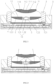
- a camera module is provided.
- the camera module includes a first lens 11, a second lens 12, and a photosensitive chip 2 that are coaxially disposed in a first direction sequentially.
- the first direction is a thickness direction of the camera module.
- a clearance is disposed between every two of the first lens 11, the second lens 12, and the photosensitive chip 2.
- a first reflective film 111 is disposed on a side of the first lens 11 away from the second lens 12.
- a second reflective film 112 is disposed on a side of the first lens 11 close to the second lens 12.
- the second lens 12 is entirely provided with a third reflective film 121 on a side close to the photosensitive chip 2.
- a light-transmitting hole 122 is provided on a middle part of the side of the second lens 12 close to the photosensitive chip 2.
- At least two adjusting lenses 13 are disposed in the light-transmitting hole 122.
- the first lens 11 is disposed above the second lens 12, and a top surface of the first lens 11 is a light input surface.
- the first reflective film 111 on the top surface of the first lens 11 can prevent light from being incident to the light-transmitting hole 122 directly; and the light is incident to the second lens 12 from a circumference on the top surface of the first lens 11.
- the third reflective film 121 is disposed on a bottom surface of the second lens 12, light cannot be incident to an interior of the camera module and be received by the photosensitive chip 2. The light is reflected to a bottom surface of the first lens 11.
- the second reflective film 112 on the bottom surface of the first lens 11 reflects the light into the light-transmitting hole 122.
- the light passes through the adjusting lenses 13 in the light-transmitting hole 122.
- the adjusting lenses 13 can disperse the light in the light-transmitting hole 122, so that the photosensitive chip 2 can receive an optical signal by a maximum area.
- the photosensitive chip 2 converts the optical signal into an electrical signal.
- the optical signal received by the photosensitive chip 2 has a larger magnification. It is also ensured that the photosensitive chip 2 can receive light by a larger area, thereby ensuring an excellent imaging effect.
- a thickness of the camera module can be decreased, too. When the camera module is mounted in an electronic device, the following case is avoided: A thickness of an electronic device is affected due to a large thickness of a camera module. This can not only increase a shooting distance of the camera module, but also decrease a thickness of the electronic device.
- a middle part on the side, away from the second lens 12, of the first lens 11 is provided with a first arc surface 113; a circumference on the side, away from the second lens 12, of the first lens 11 is a plane; the first reflective film 111 covers the first arc surface 113; the side, close to the second lens 12, of the first lens 11 is provided with a second arc surface 114; a side, away from the photosensitive chip 2, of the second lens 12 is a plane; the side, close to the photosensitive chip 2, of the second lens 12 is provided with a third arc surface 123; and the first arc surface 113, the second arc surface 114, and the third arc surface 123 are all arranged towards the first direction.
- the first arc surface 113 can not only receive more incident light, but also reflect the incident light to ensure that the incident light is emitted in a dispersed manner. This prevents the incident light from being incident and emitted perpendicularly.
- a circumference on the top surface of the first lens 11 is a plane; and a top surface of the second lens 12 is also a plane. This can ensure that more incident light is emitted to the third reflective film 121.
- the bottom surface of the first lens 11 is an arc surface; and the bottom surface of the first lens 11 is provided with the second arc surface 114. The first lens 11 can refract incident light, to ensure that the incident light can be emitted to the third reflective film 121 as much as possible.
- the third reflective film 121 can reflect more light to the second reflective film 112.
- the second reflective film 112 is disposed on the second arc surface 114.
- the arc-shaped second reflective film 112 can gather received light and reflect the light into the light-transmitting hole 122. Therefore, a quantity of optical signals that can be received by the photosensitive chip 2 is increased, thereby improving imaging quality of the camera module.
- the adjusting lenses 13 include a third lens 131 and a fourth lens 132 in the first direction sequentially; a middle part of the third lens 131 protrudes in a second direction; a middle part of the fourth lens 132 protrudes in the first direction; a central region of the fourth lens 132 protrudes in the first direction; and the first direction is opposite to the second direction.
- light is emitted to the third lens 131 in the light-transmitting hole 122.
- the third lens 131 further gathers the light, thereby avoiding loss of the light caused when the light is refracted to a hole wall of the light-transmitting hole 122.
- All light gathered by the third lens 131 is emitted to the fourth lens 132. After passing through the fourth lens 132, the light is refracted and dispersed. There is a specific clearance between the photosensitive chip 2 and the fourth lens 132.
- the fourth lens 132 is arranged close to a bottom of the light-transmitting hole 122. After the light is dispersed, the photosensitive chip 2 can receive an optical signal by a larger area.
- Shapes of the third lens 131 and the fourth lens 132 are not limited to shapes in this embodiment. Two adjusting lenses 13 are provided. An optical path may be designed more flexibly. Different shapes may be designed for the third lens 131 and the fourth lens 132 based on a reflection requirement of the optical path.
- the adjusting lenses 13 include a fifth lens.
- the fifth lens is arranged close to the photosensitive chip 2.
- the fifth lens has the same structure as the fourth lens 132. Because the fifth lens has the same structure as the fourth lens 132, light can be further dispersed. This enables the photosensitive chip 2 to receive more light, thereby improving imaging quality of the camera module.
- the fifth lens is not included in the accompanying drawings of this specification. Specifically, the fifth lens should be disposed between the fourth lens 132 and the filter.
- an area of a projection of the first reflective film 111 on the photosensitive chip 2 is greater than an aperture of the light-transmitting hole 122.
- an area of the first reflective film 111 needs to be increased, so that incident light that may be directly incident to the photosensitive chip 2 is reflected out of the camera module.
- the camera module further includes a lens assembly 1, a stabilization motor 3, a filter 4, a circuit board 5, and a bracket 6.
- the first lens 11 and the second lens 12 are mounted in the lens assembly 1.
- the lens assembly 1 is secured in the stabilization motor 3.
- the stabilization motor 3 is securely connected to the bracket 6.
- the photosensitive chip 2 is disposed in the bracket 6.
- the filter 4 is disposed between the second lens 12 and the photosensitive chip 2.
- the circuit board 5 is electrically connected to the photosensitive chip 2.
- the lens assembly 1 performs functions of transmitting, reflecting, and refracting light. After incident light is emitted to the lens assembly 1, a portion of the incident light incident to the first lens 11 is reflected by the first reflective film 111, and thus cannot pass through the first lens 11.
- the second reflective film 112 is provided with an arc surface facing the first direction, and can not only receive more reflected light, but also gather light and reflect the light into the light-transmitting hole 122.
- the filter disposed between the fifth lens and the photosensitive chip 2 is configured to achieve effects of allowing visible light to pass through and intercepting near-infrared light, thereby further improving the imaging effect of the camera module.
- the stabilization motor 3 is added. After sensing a shake in a shooting process, the stabilization motor 3 drives the lens assembly 1 to perform adjustment, thereby canceling the shake, and ensuring image stability and clear imaging.
- the circuit board 5 performs a transmission function of providing an electrical signal for the photosensitive chip 2.
- the bracket 6 provides mounting space for each structure of the camera module, and can protect a structure in the camera module from being damaged.
- the first lens 11 and the second lens 12 are glass lenses.
- the glass lenses have refractive indexes ranging from 1.34 to 1.8, and have high transmittance.
- a size of the first lens 11 that receives the light is large.
- a range of incident light is wide.
- a glass lens having a high refractive index is required, so that light can be emitted to the second lens 12 as much as possible.
- Refraction occurs when the second lens 12 receives light and reflects light.
- the second lens 12 is also required to have high transmittance and a high refractive index.
- the third lens 131, the fourth lens 132, and the fifth lens are plastic lenses.
- the plastic lenses have refractive indexes ranging from 1.5 to 1.6.
- the refractive index can meet a requirement for guiding light to the photosensitive chip 2.
- the plastic lenses are convenient to mount and have low costs, thereby lowering difficulty in production and processing.
- an area of a projection of the first lens 11 on the photosensitive chip 2 is less than an area of a projection of the second lens 12 on the photosensitive chip 2.
- a size of the second lens 12 needs to be increased, to increase utilization of incident light, ensure that a refraction effect is more diffused after incident light passes through the first lens 11, and ensure that the second reflection surface can receive more light.
- the projection of the second lens 12 on the photosensitive chip 2 covers the projection of the first lens 11 on the photosensitive chip 2. This ensures that incident light can be emitted to the photosensitive chip 2 as much as possible after a plurality of times of reflection and refraction, thereby improving the imaging effect.
- An embodiment of this application provides an electronic device.
- the electronic device is provided with the display module in any one of the above embodiments.
- the following uses mobile phones as an example.
- mobile phones in the market become increasingly thinner, to improve grip feelings of users and further improve use experience of the users.
- requirements for picture and video taking effects of mobile phones in the market are also increasingly strict.
- An imaging effect of a mobile phone affects a sales volume of the mobile phone to some extent.
- the camera module in the foregoing embodiment is used in a mobile phone, a clear long-distance picture taking effect can be achieved on the premise that a thickness of the mobile phone is not changed. This not only meets users' requirements for a hand feeling of the mobile phone, but also meets users' requirements for the picture taking effect of the mobile phone.
- FIG 2 is a diagram of an optical path of the camera module in this application. After being incident to the camera module through the top surface of the first lens 11, light is incident to the second lens 12, then reflected to the second reflective film 112 through the third reflective film 121, and finally incident to the photosensitive chip 2 after passing through the fourth lens 132 and the fifth lens in the light-transmitting hole 122.
- the photosensitive chip 2 converts an optical signal into an electrical signal, and transmits the electrical signal to the electronic device through the circuit board 5.
Landscapes
- Physics & Mathematics (AREA)
- Engineering & Computer Science (AREA)
- Multimedia (AREA)
- Signal Processing (AREA)
- General Physics & Mathematics (AREA)
- Optics & Photonics (AREA)
- Studio Devices (AREA)
- Optical Elements Other Than Lenses (AREA)
- Lens Barrels (AREA)
- Adjustment Of Camera Lenses (AREA)
- Camera Bodies And Camera Details Or Accessories (AREA)
- Cameras In General (AREA)
Abstract
Description
- This application claims priority to
Chinese Patent Application No. 202110103420.2, filed with the China National Intellectual Property Administration on January 26, 2021 - This application belongs to the technical field of consumer electronic devices, and in particular, relates to a camera module and an electronic device.
- With the development of electronic device technologies, requirements for appearances of electronic devices become increasingly high. Particularly, in the aspect of thicknesses of electronic devices, a thinner electronic device can provide a user with a better a grip feeling and improve use experience of the user. Moreover, it is necessary to meet demand of a user for using an electronic device to take pictures and videos. Therefore, manufacturers further improve an imaging effect by changing a structure of a camera module.
- For a camera module with an optical zoom, in order to increase a shooting distance of the camera module and achieve 10x or greater zooming, the camera module needs to have a longer focal length. This usually needs to increase a size of the camera module. Correspondingly, a thickness of the electronic device is increased, resulting in poor user experience.
- Therefore, it is necessary to improve a camera module of an electronic device, thereby resolving a problem that a thickness of the electronic device is increased due to an increased size of the camera module.
- Embodiments of this application aim to provide a camera module and an electronic device, thereby resolving a problem that a thickness of the electronic device is increased due to an increased size of the camera module.
- To resolve the technical problem, this application is implemented as follows.
- According to a first aspect, an embodiment of this application provides a camera module. The camera module includes a first lens, a second lens, and a photosensitive chip that are coaxially disposed in a first direction sequentially. The first direction is a thickness direction of the camera module. A clearance is disposed between every two of the first lens, the second lens, and the photosensitive chip. A first reflective film is disposed on a side of the first lens away from the second lens. A second reflective film is disposed on a side of the first lens close to the second lens. The second lens is entirely provided with a third reflective film on a side close to the photosensitive chip. A light-transmitting hole is provided on a middle part of the side of the second lens close to the photosensitive chip. At least two adjusting lenses are disposed in the light-transmitting hole.
- According to a second aspect, an embodiment of this application provides an electronic device. The electronic device is provided with the camera module described above.
- In the embodiments of this application, due to cooperation among the first reflective film, the second reflective film, and the third reflective film that are disposed on the first lens and the second lens, incident light is received by the photosensitive chip after being refracted and reflected multiple times, the photosensitive chip converts an optical signal into an electrical signal and forms an image. This decreases a total length of a lens path of the camera module without affecting imaging quality, and achieves an effect of decreasing a size of the camera module. In addition, according to this application, a structure is simple, and production is easy.
- The accompanying drawings described herein are intended to provide further understanding of this application, and constitute a part of this application. Example embodiments of this application and descriptions thereof are intended to describe this application, but do not constitute inappropriate limitations to this application. In the accompanying drawings:
-
FIG 1 is a sectional view of a camera module according to an embodiment of this application; and -
FIG 2 is a diagram of an optical path of the camera module inFIG 1 . - Reference numerals in the accompanying drawings are as follows:
1: lens assembly; 11: first lens; 111: first reflective film; 112: second reflective film; 113: first arc surface; 114: second arc surface; 12: second lens; 121: third reflective film; 122: light-transmitting hole; 123: third arc surface; 13: adjusting lens; 131: third lens; 132: fourth lens; 2: photosensitive chip; 3: stabilization motor; 4: filter; 5: circuit board; and 6: bracket. - The following clearly and completely describes technical solutions in the embodiments of this application with reference to the accompanying drawings in the embodiments of this application. Apparently, the described embodiments are some rather than all of the embodiments of this application. All other embodiments obtained by a person of ordinary skill in the art based on the embodiments of this application without creative efforts shall fall within the protection scope of this application.
- The terms "first", "second", and the like in the specification and claims of this application are used to distinguish between similar objects instead of describing a specific order or sequence. It should be understood that, data termed in such a way is interchangeable in proper circumstances, so that the embodiments of this application can be implemented in an order other than the order illustrated or described herein. In addition, in the specification and claims, "and/or" represents at least one of connected objects, and a character "/" generally represents an "or" relationship between associated objects.
- With reference to the accompanying drawings, an electronic device in an embodiment of this application is described in detail below based on specific embodiments and application scenarios thereof.
- As shown in
FIG 1 , a camera module is provided. The camera module includes afirst lens 11, asecond lens 12, and aphotosensitive chip 2 that are coaxially disposed in a first direction sequentially. The first direction is a thickness direction of the camera module. A clearance is disposed between every two of thefirst lens 11, thesecond lens 12, and thephotosensitive chip 2. A firstreflective film 111 is disposed on a side of thefirst lens 11 away from thesecond lens 12. A secondreflective film 112 is disposed on a side of thefirst lens 11 close to thesecond lens 12. Thesecond lens 12 is entirely provided with a thirdreflective film 121 on a side close to thephotosensitive chip 2. A light-transmittinghole 122 is provided on a middle part of the side of thesecond lens 12 close to thephotosensitive chip 2. At least two adjustinglenses 13 are disposed in the light-transmittinghole 122. As shown inFIG 1 , thefirst lens 11 is disposed above thesecond lens 12, and a top surface of thefirst lens 11 is a light input surface. Moreover, the firstreflective film 111 on the top surface of thefirst lens 11 can prevent light from being incident to the light-transmittinghole 122 directly; and the light is incident to thesecond lens 12 from a circumference on the top surface of thefirst lens 11. Because the thirdreflective film 121 is disposed on a bottom surface of thesecond lens 12, light cannot be incident to an interior of the camera module and be received by thephotosensitive chip 2. The light is reflected to a bottom surface of thefirst lens 11. The secondreflective film 112 on the bottom surface of thefirst lens 11 reflects the light into the light-transmittinghole 122. The light passes through the adjustinglenses 13 in the light-transmittinghole 122. The adjustinglenses 13 can disperse the light in the light-transmittinghole 122, so that thephotosensitive chip 2 can receive an optical signal by a maximum area. After receiving the optical signal, thephotosensitive chip 2 converts the optical signal into an electrical signal. After being reflected multiple times, the optical signal received by thephotosensitive chip 2 has a larger magnification. It is also ensured that thephotosensitive chip 2 can receive light by a larger area, thereby ensuring an excellent imaging effect. In addition, a thickness of the camera module can be decreased, too. When the camera module is mounted in an electronic device, the following case is avoided: A thickness of an electronic device is affected due to a large thickness of a camera module. This can not only increase a shooting distance of the camera module, but also decrease a thickness of the electronic device. - Specifically, due to cooperation between the first
reflective film 111 and the thirdreflective film 121, light can be prevented from being directly incident into the light-transmittinghole 122 and received by thephotosensitive chip 2. Therefore, a preset zoom factor is achieved. This further improves the imaging effect of the camera module. - Optionally, as shown in
FIG 1 , a middle part on the side, away from thesecond lens 12, of thefirst lens 11 is provided with afirst arc surface 113; a circumference on the side, away from thesecond lens 12, of thefirst lens 11 is a plane; the firstreflective film 111 covers thefirst arc surface 113; the side, close to thesecond lens 12, of thefirst lens 11 is provided with asecond arc surface 114; a side, away from thephotosensitive chip 2, of thesecond lens 12 is a plane; the side, close to thephotosensitive chip 2, of thesecond lens 12 is provided with athird arc surface 123; and thefirst arc surface 113, thesecond arc surface 114, and thethird arc surface 123 are all arranged towards the first direction. Thefirst arc surface 113 can not only receive more incident light, but also reflect the incident light to ensure that the incident light is emitted in a dispersed manner. This prevents the incident light from being incident and emitted perpendicularly. A circumference on the top surface of thefirst lens 11 is a plane; and a top surface of thesecond lens 12 is also a plane. This can ensure that more incident light is emitted to the thirdreflective film 121. The bottom surface of thefirst lens 11 is an arc surface; and the bottom surface of thefirst lens 11 is provided with thesecond arc surface 114. Thefirst lens 11 can refract incident light, to ensure that the incident light can be emitted to the thirdreflective film 121 as much as possible. The thirdreflective film 121 can reflect more light to the secondreflective film 112. The secondreflective film 112 is disposed on thesecond arc surface 114. The arc-shaped secondreflective film 112 can gather received light and reflect the light into the light-transmittinghole 122. Therefore, a quantity of optical signals that can be received by thephotosensitive chip 2 is increased, thereby improving imaging quality of the camera module. - Optionally, as shown in
FIG 1 , the adjustinglenses 13 include athird lens 131 and afourth lens 132 in the first direction sequentially; a middle part of thethird lens 131 protrudes in a second direction; a middle part of thefourth lens 132 protrudes in the first direction; a central region of thefourth lens 132 protrudes in the first direction; and the first direction is opposite to the second direction. After being reflected by the secondreflective film 112, light is emitted to thethird lens 131 in the light-transmittinghole 122. Thethird lens 131 further gathers the light, thereby avoiding loss of the light caused when the light is refracted to a hole wall of the light-transmittinghole 122. All light gathered by thethird lens 131 is emitted to thefourth lens 132. After passing through thefourth lens 132, the light is refracted and dispersed. There is a specific clearance between thephotosensitive chip 2 and thefourth lens 132. Thefourth lens 132 is arranged close to a bottom of the light-transmittinghole 122. After the light is dispersed, thephotosensitive chip 2 can receive an optical signal by a larger area. Shapes of thethird lens 131 and thefourth lens 132 are not limited to shapes in this embodiment. Two adjustinglenses 13 are provided. An optical path may be designed more flexibly. Different shapes may be designed for thethird lens 131 and thefourth lens 132 based on a reflection requirement of the optical path. - Optionally, the adjusting
lenses 13 include a fifth lens. The fifth lens is arranged close to thephotosensitive chip 2. The fifth lens has the same structure as thefourth lens 132. Because the fifth lens has the same structure as thefourth lens 132, light can be further dispersed. This enables thephotosensitive chip 2 to receive more light, thereby improving imaging quality of the camera module. The fifth lens is not included in the accompanying drawings of this specification. Specifically, the fifth lens should be disposed between thefourth lens 132 and the filter. - Optionally, as shown in
FIG 1 , in the first direction, an area of a projection of the firstreflective film 111 on thephotosensitive chip 2 is greater than an aperture of the light-transmittinghole 122. In order to prevent light from being directly emitted to thephotosensitive chip 2 and received by thephotosensitive chip 2, an area of the firstreflective film 111 needs to be increased, so that incident light that may be directly incident to thephotosensitive chip 2 is reflected out of the camera module. - Optionally, as shown in
FIG 1 , the camera module further includes alens assembly 1, astabilization motor 3, afilter 4, acircuit board 5, and a bracket 6. Thefirst lens 11 and thesecond lens 12 are mounted in thelens assembly 1. Thelens assembly 1 is secured in thestabilization motor 3. Thestabilization motor 3 is securely connected to the bracket 6. Thephotosensitive chip 2 is disposed in the bracket 6. Thefilter 4 is disposed between thesecond lens 12 and thephotosensitive chip 2. Thecircuit board 5 is electrically connected to thephotosensitive chip 2. Thelens assembly 1 performs functions of transmitting, reflecting, and refracting light. After incident light is emitted to thelens assembly 1, a portion of the incident light incident to thefirst lens 11 is reflected by the firstreflective film 111, and thus cannot pass through thefirst lens 11. Light incident to the circumference on the top surface of thefirst lens 11 passes through thefirst lens 11, and is emitted from the top surface of thesecond lens 12 to the bottom surface of thesecond lens 12 after being refracted by thefirst lens 11. After being reflected by the thirdreflective film 121 on the bottom surface of thesecond lens 12, light is emitted to the secondreflective film 112 on the bottom surface of thefirst lens 11. The secondreflective film 112 is provided with an arc surface facing the first direction, and can not only receive more reflected light, but also gather light and reflect the light into the light-transmittinghole 122. After passing through thethird lens 131, light is refracted and is gathered in an axial direction of thelens assembly 1, so that the light is prevented from being emitted to the hole wall of the light-transmittinghole 122. After passing through thethird lens 131, the light passes through thefourth lens 132 and the fifth lens respectively. Thefourth lens 132 and the fifth lens disperse the light in directions away from the axial direction of thelens assembly 1, so that the light can be scattered over thephotosensitive chip 2 as uniform as possible. In addition, the filter disposed between the fifth lens and thephotosensitive chip 2 is configured to achieve effects of allowing visible light to pass through and intercepting near-infrared light, thereby further improving the imaging effect of the camera module. Because a magnification of the camera module is large, a slight shake during shooting with a large magnification leads to a blurred image. For this reason, thestabilization motor 3 is added. After sensing a shake in a shooting process, thestabilization motor 3 drives thelens assembly 1 to perform adjustment, thereby canceling the shake, and ensuring image stability and clear imaging. Thecircuit board 5 performs a transmission function of providing an electrical signal for thephotosensitive chip 2. The bracket 6 provides mounting space for each structure of the camera module, and can protect a structure in the camera module from being damaged. - Optionally, as shown in
FIG 1 , thefirst lens 11 and thesecond lens 12 are glass lenses. The glass lenses have refractive indexes ranging from 1.34 to 1.8, and have high transmittance. In an incident process of light, a size of thefirst lens 11 that receives the light is large. Correspondingly, a range of incident light is wide. In this case, a glass lens having a high refractive index is required, so that light can be emitted to thesecond lens 12 as much as possible. Refraction occurs when thesecond lens 12 receives light and reflects light. To ensure that sufficient light can be incident to the secondreflective film 112, thesecond lens 12 is also required to have high transmittance and a high refractive index. - Optionally, as shown in
FIG 1 , thethird lens 131, thefourth lens 132, and the fifth lens are plastic lenses. The plastic lenses have refractive indexes ranging from 1.5 to 1.6. The refractive index can meet a requirement for guiding light to thephotosensitive chip 2. Moreover, the plastic lenses are convenient to mount and have low costs, thereby lowering difficulty in production and processing. - Optionally, as shown in
FIG 1 , in the first direction, an area of a projection of thefirst lens 11 on thephotosensitive chip 2 is less than an area of a projection of thesecond lens 12 on thephotosensitive chip 2. A size of thesecond lens 12 needs to be increased, to increase utilization of incident light, ensure that a refraction effect is more diffused after incident light passes through thefirst lens 11, and ensure that the second reflection surface can receive more light. Because thefirst lens 11 and thesecond lens 12 are disposed coaxially, the projection of thesecond lens 12 on thephotosensitive chip 2 covers the projection of thefirst lens 11 on thephotosensitive chip 2. This ensures that incident light can be emitted to thephotosensitive chip 2 as much as possible after a plurality of times of reflection and refraction, thereby improving the imaging effect. - An embodiment of this application provides an electronic device. The electronic device is provided with the display module in any one of the above embodiments. The following uses mobile phones as an example. Nowadays, mobile phones in the market become increasingly thinner, to improve grip feelings of users and further improve use experience of the users. However, requirements for picture and video taking effects of mobile phones in the market are also increasingly strict. An imaging effect of a mobile phone affects a sales volume of the mobile phone to some extent. When the camera module in the foregoing embodiment is used in a mobile phone, a clear long-distance picture taking effect can be achieved on the premise that a thickness of the mobile phone is not changed. This not only meets users' requirements for a hand feeling of the mobile phone, but also meets users' requirements for the picture taking effect of the mobile phone.
- Specifically,
FIG 2 is a diagram of an optical path of the camera module in this application. After being incident to the camera module through the top surface of thefirst lens 11, light is incident to thesecond lens 12, then reflected to the secondreflective film 112 through the thirdreflective film 121, and finally incident to thephotosensitive chip 2 after passing through thefourth lens 132 and the fifth lens in the light-transmittinghole 122. Thephotosensitive chip 2 converts an optical signal into an electrical signal, and transmits the electrical signal to the electronic device through thecircuit board 5. - The embodiments of this application are described above with reference to the accompanying drawings. However, this application is not limited to the foregoing specific implementations. The foregoing specific implementations are merely illustrative instead of restrictive. Under the enlightenment of this application, a person of ordinary skill in the art may make many forms without departing from the essence of this application and the protection scope of claims, all of which fall within the protection of this application.
Claims (10)
- A camera module, wherein the camera module comprises a first lens, a second lens, and a photosensitive chip that are coaxially disposed in a first direction sequentially, the first direction is a thickness direction of the camera module, a clearance is disposed between every two of the first lens, the second lens, and the photosensitive chip, a first reflective film is disposed on a side of the first lens away from the second lens, a second reflective film is disposed on a side of the first lens close to the second lens, the second lens is entirely provided with a third reflective film on a side close to the photosensitive chip, a light-transmitting hole is provided on a middle part of the side of the second lens close to the photosensitive chip, and at least two adjusting lenses are disposed in the light-transmitting hole.
- The camera module according to claim 1, wherein a middle part on the side, away from the second lens, of the first lens is provided with a first arc surface, a circumference on the side, away from the second lens, of the first lens is a plane, the first reflective film covers the first arc surface, the side, close to the second lens, of the first lens is provided with a second arc surface, a side, away from the photosensitive chip, of the second lens is a plane, the side, close to the photosensitive chip, of the second lens is provided with a third arc surface, and the first arc surface, the second arc surface, and the third arc surface are all arranged towards the first direction.
- The camera module according to claim 1, wherein the adjusting lenses comprise a third lens and a fourth lens in the first direction sequentially, a middle part of the third lens protrudes in a second direction, a middle part of the fourth lens protrudes in the first direction, a central region of the fourth lens protrudes in the first direction, and the first direction is opposite to the second direction.
- The camera module according to claim 3, wherein the adjusting lenses comprise a fifth lens, the fifth lens is arranged close to the photosensitive chip, the fifth lens has the same structure as the fourth lens.
- The camera module according to claim 1, wherein in the first direction, an area of a projection of the first reflective film on the photosensitive chip is greater than an aperture of the light-transmitting hole.
- The camera module according to claim 1, wherein the camera module further comprises a lens assembly, a stabilization motor, a filter, a circuit board, and a bracket, the first lens and the second lens are mounted in the lens assembly, the lens assembly is secured in the stabilization motor, the stabilization motor is securely connected to the bracket, the photosensitive chip is disposed in the bracket, the filter is disposed between the second lens and the photosensitive chip, and the circuit board is electrically connected to the photosensitive chip.
- The camera module according to claim 1, wherein the first lens and the second lens are glass lenses.
- The camera module according to claim 4, wherein the third lens, the fourth lens, and the fifth lens are plastic lenses.
- The camera module according to claim 1, wherein in the first direction, an area of a projection of the first lens on the photosensitive chip is less than an area of a projection of the second lens on the photosensitive chip.
- An electronic device, wherein the electronic device is provided with the camera module according to any one of claims 1 to 9.
Applications Claiming Priority (2)
| Application Number | Priority Date | Filing Date | Title |
|---|---|---|---|
| CN202110103420.2A CN112887564B (en) | 2021-01-26 | 2021-01-26 | Camera module and electronic equipment |
| PCT/CN2022/072862 WO2022161232A1 (en) | 2021-01-26 | 2022-01-20 | Camera module and electronic device |
Publications (3)
| Publication Number | Publication Date |
|---|---|
| EP4287609A1 true EP4287609A1 (en) | 2023-12-06 |
| EP4287609A4 EP4287609A4 (en) | 2024-07-24 |
| EP4287609B1 EP4287609B1 (en) | 2025-05-21 |
Family
ID=76053434
Family Applications (1)
| Application Number | Title | Priority Date | Filing Date |
|---|---|---|---|
| EP22745107.7A Active EP4287609B1 (en) | 2021-01-26 | 2022-01-20 | Camera module and electronic device |
Country Status (6)
| Country | Link |
|---|---|
| US (1) | US12316943B2 (en) |
| EP (1) | EP4287609B1 (en) |
| JP (1) | JP7628619B2 (en) |
| CN (1) | CN112887564B (en) |
| ES (1) | ES3033723T3 (en) |
| WO (1) | WO2022161232A1 (en) |
Families Citing this family (3)
| Publication number | Priority date | Publication date | Assignee | Title |
|---|---|---|---|---|
| CN112887564B (en) * | 2021-01-26 | 2022-03-29 | 维沃移动通信有限公司 | Camera module and electronic equipment |
| CN114089582A (en) * | 2021-11-16 | 2022-02-25 | Oppo广东移动通信有限公司 | Shading assembly and preparation method thereof, optical lens, camera and electronic equipment |
| CN114222054A (en) * | 2022-01-14 | 2022-03-22 | 维沃移动通信有限公司 | Camera module and electronic equipment |
Family Cites Families (21)
| Publication number | Priority date | Publication date | Assignee | Title |
|---|---|---|---|---|
| US4342503A (en) * | 1979-10-09 | 1982-08-03 | The Perkin-Elmer Corporation | Catadioptric telescopes |
| US5159495A (en) * | 1990-12-11 | 1992-10-27 | Eastman Kodak Company | Graded index optical elements and catadioptric optical systems |
| JPH11316343A (en) * | 1998-05-01 | 1999-11-16 | Nikon Corp | Catadioptric lens |
| TWI561884B (en) * | 2010-04-06 | 2016-12-11 | Hon Hai Prec Ind Co Ltd | Camera module and method for making same |
| KR20140024647A (en) * | 2012-08-20 | 2014-03-03 | 삼성전자주식회사 | Reflective type telephoto lens and photographing apparatus |
| US9507129B2 (en) * | 2013-10-31 | 2016-11-29 | Duke University | Apparatus comprising a compact catadioptric telescope |
| JP6917000B2 (en) * | 2016-12-28 | 2021-08-11 | 株式会社タムロン | Catadioptric system and imaging device |
| CN108363159B (en) * | 2017-01-26 | 2023-04-07 | 宁波舜宇光电信息有限公司 | Lens, camera module and manufacturing method thereof |
| US10606050B2 (en) * | 2017-03-06 | 2020-03-31 | Fotonation Limited | Portrait lens system suitable for use in a mobile camera |
| CN107561684B (en) * | 2017-09-30 | 2021-02-23 | Oppo广东移动通信有限公司 | Filters, Lens Modules and Imaging Modules |
| CN110381230A (en) * | 2018-04-13 | 2019-10-25 | 甘肃智呈网络科技有限公司 | A kind of binocular camera shooting device of preposition beam-splitting structure |
| US12066609B2 (en) * | 2018-06-27 | 2024-08-20 | The Charles Stark Draper Laboratory, Inc. | Multiple effective focal length (EFL) optical system |
| US10935780B2 (en) | 2018-10-04 | 2021-03-02 | Lawrence Livermore National Security, Llc | Integrated telescope for imaging applications |
| CN109194859B (en) * | 2018-10-31 | 2020-09-04 | 维沃移动通信(杭州)有限公司 | Camera and terminal equipment |
| CN210155397U (en) * | 2019-05-23 | 2020-03-17 | 鑫视科技股份有限公司 | Plug-and-play light camera lens device |
| CA3145526A1 (en) * | 2019-06-28 | 2020-12-30 | Lumenuity, Llc | Systems and methods for high-magnification high-resolution photography using a small imaging system |
| CN110888216B (en) * | 2019-11-04 | 2021-10-22 | 荣耀终端有限公司 | Optical lenses, lens modules and terminals |
| CN110798602B (en) * | 2019-11-29 | 2022-08-19 | 维沃移动通信有限公司 | Camera module, electronic equipment, shooting control method and device |
| CN111601026B (en) | 2020-05-28 | 2021-12-07 | 维沃移动通信(杭州)有限公司 | Camera module and electronic equipment |
| JP7051940B2 (en) * | 2020-06-23 | 2022-04-11 | エーエーシー オプティックス ソリューションズ ピーティーイー リミテッド | Imaging lens of catadioptric system |
| CN112887564B (en) * | 2021-01-26 | 2022-03-29 | 维沃移动通信有限公司 | Camera module and electronic equipment |
-
2021
- 2021-01-26 CN CN202110103420.2A patent/CN112887564B/en active Active
-
2022
- 2022-01-20 EP EP22745107.7A patent/EP4287609B1/en active Active
- 2022-01-20 ES ES22745107T patent/ES3033723T3/en active Active
- 2022-01-20 WO PCT/CN2022/072862 patent/WO2022161232A1/en not_active Ceased
- 2022-01-20 JP JP2023544750A patent/JP7628619B2/en active Active
-
2023
- 2023-07-24 US US18/357,290 patent/US12316943B2/en active Active
Also Published As
| Publication number | Publication date |
|---|---|
| CN112887564A (en) | 2021-06-01 |
| EP4287609B1 (en) | 2025-05-21 |
| US12316943B2 (en) | 2025-05-27 |
| US20240022804A1 (en) | 2024-01-18 |
| JP7628619B2 (en) | 2025-02-10 |
| JP2024504436A (en) | 2024-01-31 |
| ES3033723T3 (en) | 2025-08-07 |
| CN112887564B (en) | 2022-03-29 |
| WO2022161232A1 (en) | 2022-08-04 |
| EP4287609A4 (en) | 2024-07-24 |
Similar Documents
| Publication | Publication Date | Title |
|---|---|---|
| CN219370111U (en) | Optical imaging system, camera module and electronic equipment | |
| US12316943B2 (en) | Camera module and electronic device employing a catadioptric lens arrangement | |
| KR102780677B1 (en) | Lens assemblies, cameras, and electronic devices | |
| TW202113448A (en) | Camera module and electronic device | |
| CN218272884U (en) | Optical imaging system, camera module and electronic equipment | |
| WO2024098911A9 (en) | Optical lens, camera module, and electronic device | |
| WO2024104120A1 (en) | Camera module and electronic device | |
| US20210029231A1 (en) | Camera Module and Electronic Device | |
| CN113645373B (en) | Periscopic module of making a video recording, make a video recording module and electronic equipment more | |
| CN111474665A (en) | Optical lens, lens module using same and electronic device | |
| WO2025218019A1 (en) | Camera module and electronic device | |
| KR102800184B1 (en) | Liquid Lens, Camera Module, And Optical Device | |
| CN212675341U (en) | Optical imaging lens group | |
| CN114859511A (en) | Optical lens, camera module and electronic equipment | |
| US11480852B2 (en) | Camera module and electronic apparatus | |
| US11317011B2 (en) | Terminal device | |
| CN119678083A (en) | Lenses, camera modules and electronic devices | |
| CN114415342A (en) | Zoom lens and terminal equipment | |
| CN115242904A (en) | Electronic equipment | |
| CN116136620A (en) | Optical lens, camera module and terminal equipment | |
| CN120103586B (en) | Optical lens, camera module and electronic equipment | |
| CN223502942U (en) | Camera modules and electronic devices | |
| CN112835175A (en) | A camera module and terminal equipment | |
| CN216930151U (en) | Take camera glass lid of CD line | |
| CN210469509U (en) | Camera module with long focus mode and electronic equipment |
Legal Events
| Date | Code | Title | Description |
|---|---|---|---|
| STAA | Information on the status of an ep patent application or granted ep patent |
Free format text: STATUS: THE INTERNATIONAL PUBLICATION HAS BEEN MADE |
|
| PUAI | Public reference made under article 153(3) epc to a published international application that has entered the european phase |
Free format text: ORIGINAL CODE: 0009012 |
|
| STAA | Information on the status of an ep patent application or granted ep patent |
Free format text: STATUS: REQUEST FOR EXAMINATION WAS MADE |
|
| 17P | Request for examination filed |
Effective date: 20230816 |
|
| AK | Designated contracting states |
Kind code of ref document: A1 Designated state(s): AL AT BE BG CH CY CZ DE DK EE ES FI FR GB GR HR HU IE IS IT LI LT LU LV MC MK MT NL NO PL PT RO RS SE SI SK SM TR |
|
| DAV | Request for validation of the european patent (deleted) | ||
| DAX | Request for extension of the european patent (deleted) | ||
| REG | Reference to a national code |
Ref country code: DE Ref legal event code: R079 Free format text: PREVIOUS MAIN CLASS: H04N0005225000 Ipc: G02B0013000000 Ref document number: 602022014991 Country of ref document: DE |
|
| A4 | Supplementary search report drawn up and despatched |
Effective date: 20240619 |
|
| RIC1 | Information provided on ipc code assigned before grant |
Ipc: H04N 23/55 20230101ALI20240614BHEP Ipc: G03B 30/00 20210101ALI20240614BHEP Ipc: G03B 17/17 20210101ALI20240614BHEP Ipc: G02B 17/08 20060101ALI20240614BHEP Ipc: G02B 13/00 20060101AFI20240614BHEP |
|
| GRAP | Despatch of communication of intention to grant a patent |
Free format text: ORIGINAL CODE: EPIDOSNIGR1 |
|
| STAA | Information on the status of an ep patent application or granted ep patent |
Free format text: STATUS: GRANT OF PATENT IS INTENDED |
|
| INTG | Intention to grant announced |
Effective date: 20250129 |
|
| GRAS | Grant fee paid |
Free format text: ORIGINAL CODE: EPIDOSNIGR3 |
|
| GRAA | (expected) grant |
Free format text: ORIGINAL CODE: 0009210 |
|
| STAA | Information on the status of an ep patent application or granted ep patent |
Free format text: STATUS: THE PATENT HAS BEEN GRANTED |
|
| AK | Designated contracting states |
Kind code of ref document: B1 Designated state(s): AL AT BE BG CH CY CZ DE DK EE ES FI FR GB GR HR HU IE IS IT LI LT LU LV MC MK MT NL NO PL PT RO RS SE SI SK SM TR |
|
| REG | Reference to a national code |
Ref country code: GB Ref legal event code: FG4D |
|
| REG | Reference to a national code |
Ref country code: CH Ref legal event code: EP |
|
| REG | Reference to a national code |
Ref country code: DE Ref legal event code: R096 Ref document number: 602022014991 Country of ref document: DE |
|
| REG | Reference to a national code |
Ref country code: IE Ref legal event code: FG4D |
|
| REG | Reference to a national code |
Ref country code: NL Ref legal event code: FP |
|
| REG | Reference to a national code |
Ref country code: ES Ref legal event code: FG2A Ref document number: 3033723 Country of ref document: ES Kind code of ref document: T3 Effective date: 20250807 |
|
| PG25 | Lapsed in a contracting state [announced via postgrant information from national office to epo] |
Ref country code: FI Free format text: LAPSE BECAUSE OF FAILURE TO SUBMIT A TRANSLATION OF THE DESCRIPTION OR TO PAY THE FEE WITHIN THE PRESCRIBED TIME-LIMIT Effective date: 20250521 Ref country code: PT Free format text: LAPSE BECAUSE OF FAILURE TO SUBMIT A TRANSLATION OF THE DESCRIPTION OR TO PAY THE FEE WITHIN THE PRESCRIBED TIME-LIMIT Effective date: 20250922 |
|
| REG | Reference to a national code |
Ref country code: LT Ref legal event code: MG9D |
|
| PG25 | Lapsed in a contracting state [announced via postgrant information from national office to epo] |
Ref country code: GR Free format text: LAPSE BECAUSE OF FAILURE TO SUBMIT A TRANSLATION OF THE DESCRIPTION OR TO PAY THE FEE WITHIN THE PRESCRIBED TIME-LIMIT Effective date: 20250822 Ref country code: NO Free format text: LAPSE BECAUSE OF FAILURE TO SUBMIT A TRANSLATION OF THE DESCRIPTION OR TO PAY THE FEE WITHIN THE PRESCRIBED TIME-LIMIT Effective date: 20250821 |
|
| PG25 | Lapsed in a contracting state [announced via postgrant information from national office to epo] |
Ref country code: PL Free format text: LAPSE BECAUSE OF FAILURE TO SUBMIT A TRANSLATION OF THE DESCRIPTION OR TO PAY THE FEE WITHIN THE PRESCRIBED TIME-LIMIT Effective date: 20250521 |
|
| PG25 | Lapsed in a contracting state [announced via postgrant information from national office to epo] |
Ref country code: BG Free format text: LAPSE BECAUSE OF FAILURE TO SUBMIT A TRANSLATION OF THE DESCRIPTION OR TO PAY THE FEE WITHIN THE PRESCRIBED TIME-LIMIT Effective date: 20250521 |
|
| PG25 | Lapsed in a contracting state [announced via postgrant information from national office to epo] |
Ref country code: HR Free format text: LAPSE BECAUSE OF FAILURE TO SUBMIT A TRANSLATION OF THE DESCRIPTION OR TO PAY THE FEE WITHIN THE PRESCRIBED TIME-LIMIT Effective date: 20250521 |
|
| PG25 | Lapsed in a contracting state [announced via postgrant information from national office to epo] |
Ref country code: RS Free format text: LAPSE BECAUSE OF FAILURE TO SUBMIT A TRANSLATION OF THE DESCRIPTION OR TO PAY THE FEE WITHIN THE PRESCRIBED TIME-LIMIT Effective date: 20250821 |
|
| PG25 | Lapsed in a contracting state [announced via postgrant information from national office to epo] |
Ref country code: IS Free format text: LAPSE BECAUSE OF FAILURE TO SUBMIT A TRANSLATION OF THE DESCRIPTION OR TO PAY THE FEE WITHIN THE PRESCRIBED TIME-LIMIT Effective date: 20250921 |
|
| PG25 | Lapsed in a contracting state [announced via postgrant information from national office to epo] |
Ref country code: LV Free format text: LAPSE BECAUSE OF FAILURE TO SUBMIT A TRANSLATION OF THE DESCRIPTION OR TO PAY THE FEE WITHIN THE PRESCRIBED TIME-LIMIT Effective date: 20250521 |
|
| REG | Reference to a national code |
Ref country code: AT Ref legal event code: MK05 Ref document number: 1797218 Country of ref document: AT Kind code of ref document: T Effective date: 20250521 |
|
| PGFP | Annual fee paid to national office [announced via postgrant information from national office to epo] |
Ref country code: GB Payment date: 20251127 Year of fee payment: 5 |
|
| PG25 | Lapsed in a contracting state [announced via postgrant information from national office to epo] |
Ref country code: SM Free format text: LAPSE BECAUSE OF FAILURE TO SUBMIT A TRANSLATION OF THE DESCRIPTION OR TO PAY THE FEE WITHIN THE PRESCRIBED TIME-LIMIT Effective date: 20250521 Ref country code: DK Free format text: LAPSE BECAUSE OF FAILURE TO SUBMIT A TRANSLATION OF THE DESCRIPTION OR TO PAY THE FEE WITHIN THE PRESCRIBED TIME-LIMIT Effective date: 20250521 Ref country code: AT Free format text: LAPSE BECAUSE OF FAILURE TO SUBMIT A TRANSLATION OF THE DESCRIPTION OR TO PAY THE FEE WITHIN THE PRESCRIBED TIME-LIMIT Effective date: 20250521 |
|
| PGFP | Annual fee paid to national office [announced via postgrant information from national office to epo] |
Ref country code: FR Payment date: 20251128 Year of fee payment: 5 Ref country code: NL Payment date: 20251215 Year of fee payment: 5 |
|
| PG25 | Lapsed in a contracting state [announced via postgrant information from national office to epo] |
Ref country code: CZ Free format text: LAPSE BECAUSE OF FAILURE TO SUBMIT A TRANSLATION OF THE DESCRIPTION OR TO PAY THE FEE WITHIN THE PRESCRIBED TIME-LIMIT Effective date: 20250521 |
|
| PG25 | Lapsed in a contracting state [announced via postgrant information from national office to epo] |
Ref country code: EE Free format text: LAPSE BECAUSE OF FAILURE TO SUBMIT A TRANSLATION OF THE DESCRIPTION OR TO PAY THE FEE WITHIN THE PRESCRIBED TIME-LIMIT Effective date: 20250521 |
|
| PG25 | Lapsed in a contracting state [announced via postgrant information from national office to epo] |
Ref country code: SK Free format text: LAPSE BECAUSE OF FAILURE TO SUBMIT A TRANSLATION OF THE DESCRIPTION OR TO PAY THE FEE WITHIN THE PRESCRIBED TIME-LIMIT Effective date: 20250521 |
|
| REG | Reference to a national code |
Ref country code: DE Ref legal event code: R097 Ref document number: 602022014991 Country of ref document: DE |
|
| PLBE | No opposition filed within time limit |
Free format text: ORIGINAL CODE: 0009261 |
|
| STAA | Information on the status of an ep patent application or granted ep patent |
Free format text: STATUS: NO OPPOSITION FILED WITHIN TIME LIMIT |
|
| REG | Reference to a national code |
Ref country code: CH Ref legal event code: L10 Free format text: ST27 STATUS EVENT CODE: U-0-0-L10-L00 (AS PROVIDED BY THE NATIONAL OFFICE) Effective date: 20260402 |
|
| PGFP | Annual fee paid to national office [announced via postgrant information from national office to epo] |
Ref country code: ES Payment date: 20260213 Year of fee payment: 5 |
|
| PGFP | Annual fee paid to national office [announced via postgrant information from national office to epo] |
Ref country code: DE Payment date: 20251203 Year of fee payment: 5 |
|
| PGFP | Annual fee paid to national office [announced via postgrant information from national office to epo] |
Ref country code: IT Payment date: 20251219 Year of fee payment: 5 |
|
| 26N | No opposition filed |
Effective date: 20260224 |