EP4287481A1 - Low voltage buck regulator voltage regulation with reduced overshoot and settling time - Google Patents
Low voltage buck regulator voltage regulation with reduced overshoot and settling time Download PDFInfo
- Publication number
- EP4287481A1 EP4287481A1 EP23176224.6A EP23176224A EP4287481A1 EP 4287481 A1 EP4287481 A1 EP 4287481A1 EP 23176224 A EP23176224 A EP 23176224A EP 4287481 A1 EP4287481 A1 EP 4287481A1
- Authority
- EP
- European Patent Office
- Prior art keywords
- voltage
- output
- circuit
- power converter
- suppression circuit
- Prior art date
- Legal status (The legal status is an assumption and is not a legal conclusion. Google has not performed a legal analysis and makes no representation as to the accuracy of the status listed.)
- Pending
Links
- 230000001629 suppression Effects 0.000 claims abstract description 48
- 230000001052 transient effect Effects 0.000 claims abstract description 27
- 239000003990 capacitor Substances 0.000 claims description 16
- 238000004088 simulation Methods 0.000 description 3
- 230000002159 abnormal effect Effects 0.000 description 2
- 230000008901 benefit Effects 0.000 description 2
- 238000004146 energy storage Methods 0.000 description 2
- 230000004048 modification Effects 0.000 description 2
- 238000012986 modification Methods 0.000 description 2
- 239000000463 material Substances 0.000 description 1
- 238000005259 measurement Methods 0.000 description 1
- 238000000034 method Methods 0.000 description 1
- 230000007935 neutral effect Effects 0.000 description 1
- 230000000630 rising effect Effects 0.000 description 1
Images


Classifications
-
- H—ELECTRICITY
- H02—GENERATION; CONVERSION OR DISTRIBUTION OF ELECTRIC POWER
- H02M—APPARATUS FOR CONVERSION BETWEEN AC AND AC, BETWEEN AC AND DC, OR BETWEEN DC AND DC, AND FOR USE WITH MAINS OR SIMILAR POWER SUPPLY SYSTEMS; CONVERSION OF DC OR AC INPUT POWER INTO SURGE OUTPUT POWER; CONTROL OR REGULATION THEREOF
- H02M3/00—Conversion of DC power input into DC power output
- H02M3/02—Conversion of DC power input into DC power output without intermediate conversion into AC
- H02M3/04—Conversion of DC power input into DC power output without intermediate conversion into AC by static converters
- H02M3/10—Conversion of DC power input into DC power output without intermediate conversion into AC by static converters using discharge tubes with control electrode or semiconductor devices with control electrode
- H02M3/145—Conversion of DC power input into DC power output without intermediate conversion into AC by static converters using discharge tubes with control electrode or semiconductor devices with control electrode using devices of a triode or transistor type requiring continuous application of a control signal
- H02M3/155—Conversion of DC power input into DC power output without intermediate conversion into AC by static converters using discharge tubes with control electrode or semiconductor devices with control electrode using devices of a triode or transistor type requiring continuous application of a control signal using semiconductor devices only
- H02M3/156—Conversion of DC power input into DC power output without intermediate conversion into AC by static converters using discharge tubes with control electrode or semiconductor devices with control electrode using devices of a triode or transistor type requiring continuous application of a control signal using semiconductor devices only with automatic control of output voltage or current, e.g. switching regulators
-
- H—ELECTRICITY
- H02—GENERATION; CONVERSION OR DISTRIBUTION OF ELECTRIC POWER
- H02M—APPARATUS FOR CONVERSION BETWEEN AC AND AC, BETWEEN AC AND DC, OR BETWEEN DC AND DC, AND FOR USE WITH MAINS OR SIMILAR POWER SUPPLY SYSTEMS; CONVERSION OF DC OR AC INPUT POWER INTO SURGE OUTPUT POWER; CONTROL OR REGULATION THEREOF
- H02M3/00—Conversion of DC power input into DC power output
- H02M3/02—Conversion of DC power input into DC power output without intermediate conversion into AC
- H02M3/04—Conversion of DC power input into DC power output without intermediate conversion into AC by static converters
- H02M3/10—Conversion of DC power input into DC power output without intermediate conversion into AC by static converters using discharge tubes with control electrode or semiconductor devices with control electrode
- H02M3/145—Conversion of DC power input into DC power output without intermediate conversion into AC by static converters using discharge tubes with control electrode or semiconductor devices with control electrode using devices of a triode or transistor type requiring continuous application of a control signal
- H02M3/155—Conversion of DC power input into DC power output without intermediate conversion into AC by static converters using discharge tubes with control electrode or semiconductor devices with control electrode using devices of a triode or transistor type requiring continuous application of a control signal using semiconductor devices only
- H02M3/156—Conversion of DC power input into DC power output without intermediate conversion into AC by static converters using discharge tubes with control electrode or semiconductor devices with control electrode using devices of a triode or transistor type requiring continuous application of a control signal using semiconductor devices only with automatic control of output voltage or current, e.g. switching regulators
- H02M3/158—Conversion of DC power input into DC power output without intermediate conversion into AC by static converters using discharge tubes with control electrode or semiconductor devices with control electrode using devices of a triode or transistor type requiring continuous application of a control signal using semiconductor devices only with automatic control of output voltage or current, e.g. switching regulators including plural semiconductor devices as final control devices for a single load
-
- H—ELECTRICITY
- H02—GENERATION; CONVERSION OR DISTRIBUTION OF ELECTRIC POWER
- H02M—APPARATUS FOR CONVERSION BETWEEN AC AND AC, BETWEEN AC AND DC, OR BETWEEN DC AND DC, AND FOR USE WITH MAINS OR SIMILAR POWER SUPPLY SYSTEMS; CONVERSION OF DC OR AC INPUT POWER INTO SURGE OUTPUT POWER; CONTROL OR REGULATION THEREOF
- H02M3/00—Conversion of DC power input into DC power output
- H02M3/02—Conversion of DC power input into DC power output without intermediate conversion into AC
- H02M3/04—Conversion of DC power input into DC power output without intermediate conversion into AC by static converters
- H02M3/10—Conversion of DC power input into DC power output without intermediate conversion into AC by static converters using discharge tubes with control electrode or semiconductor devices with control electrode
- H02M3/145—Conversion of DC power input into DC power output without intermediate conversion into AC by static converters using discharge tubes with control electrode or semiconductor devices with control electrode using devices of a triode or transistor type requiring continuous application of a control signal
- H02M3/155—Conversion of DC power input into DC power output without intermediate conversion into AC by static converters using discharge tubes with control electrode or semiconductor devices with control electrode using devices of a triode or transistor type requiring continuous application of a control signal using semiconductor devices only
- H02M3/156—Conversion of DC power input into DC power output without intermediate conversion into AC by static converters using discharge tubes with control electrode or semiconductor devices with control electrode using devices of a triode or transistor type requiring continuous application of a control signal using semiconductor devices only with automatic control of output voltage or current, e.g. switching regulators
- H02M3/1566—Conversion of DC power input into DC power output without intermediate conversion into AC by static converters using discharge tubes with control electrode or semiconductor devices with control electrode using devices of a triode or transistor type requiring continuous application of a control signal using semiconductor devices only with automatic control of output voltage or current, e.g. switching regulators with means for compensating against rapid load changes, e.g. with auxiliary current source, with dual mode control or with inductance variation
-
- H—ELECTRICITY
- H02—GENERATION; CONVERSION OR DISTRIBUTION OF ELECTRIC POWER
- H02M—APPARATUS FOR CONVERSION BETWEEN AC AND AC, BETWEEN AC AND DC, OR BETWEEN DC AND DC, AND FOR USE WITH MAINS OR SIMILAR POWER SUPPLY SYSTEMS; CONVERSION OF DC OR AC INPUT POWER INTO SURGE OUTPUT POWER; CONTROL OR REGULATION THEREOF
- H02M1/00—Details of apparatus for conversion
- H02M1/0003—Details of control, feedback or regulation circuits
- H02M1/0016—Control circuits providing compensation of output voltage deviations using feedforward of disturbance parameters
- H02M1/0019—Control circuits providing compensation of output voltage deviations using feedforward of disturbance parameters the disturbance parameters being load current fluctuations
-
- H—ELECTRICITY
- H02—GENERATION; CONVERSION OR DISTRIBUTION OF ELECTRIC POWER
- H02M—APPARATUS FOR CONVERSION BETWEEN AC AND AC, BETWEEN AC AND DC, OR BETWEEN DC AND DC, AND FOR USE WITH MAINS OR SIMILAR POWER SUPPLY SYSTEMS; CONVERSION OF DC OR AC INPUT POWER INTO SURGE OUTPUT POWER; CONTROL OR REGULATION THEREOF
- H02M1/00—Details of apparatus for conversion
- H02M1/0003—Details of control, feedback or regulation circuits
- H02M1/0038—Circuits or arrangements for suppressing, e.g. by masking incorrect turn-on or turn-off signals, e.g. due to current spikes in current mode control
-
- H—ELECTRICITY
- H02—GENERATION; CONVERSION OR DISTRIBUTION OF ELECTRIC POWER
- H02M—APPARATUS FOR CONVERSION BETWEEN AC AND AC, BETWEEN AC AND DC, OR BETWEEN DC AND DC, AND FOR USE WITH MAINS OR SIMILAR POWER SUPPLY SYSTEMS; CONVERSION OF DC OR AC INPUT POWER INTO SURGE OUTPUT POWER; CONTROL OR REGULATION THEREOF
- H02M3/00—Conversion of DC power input into DC power output
- H02M3/02—Conversion of DC power input into DC power output without intermediate conversion into AC
- H02M3/04—Conversion of DC power input into DC power output without intermediate conversion into AC by static converters
- H02M3/10—Conversion of DC power input into DC power output without intermediate conversion into AC by static converters using discharge tubes with control electrode or semiconductor devices with control electrode
- H02M3/145—Conversion of DC power input into DC power output without intermediate conversion into AC by static converters using discharge tubes with control electrode or semiconductor devices with control electrode using devices of a triode or transistor type requiring continuous application of a control signal
- H02M3/155—Conversion of DC power input into DC power output without intermediate conversion into AC by static converters using discharge tubes with control electrode or semiconductor devices with control electrode using devices of a triode or transistor type requiring continuous application of a control signal using semiconductor devices only
- H02M3/156—Conversion of DC power input into DC power output without intermediate conversion into AC by static converters using discharge tubes with control electrode or semiconductor devices with control electrode using devices of a triode or transistor type requiring continuous application of a control signal using semiconductor devices only with automatic control of output voltage or current, e.g. switching regulators
- H02M3/157—Conversion of DC power input into DC power output without intermediate conversion into AC by static converters using discharge tubes with control electrode or semiconductor devices with control electrode using devices of a triode or transistor type requiring continuous application of a control signal using semiconductor devices only with automatic control of output voltage or current, e.g. switching regulators with digital control
-
- H—ELECTRICITY
- H03—ELECTRONIC CIRCUITRY
- H03K—PULSE TECHNIQUE
- H03K3/00—Circuits for generating electric pulses; Monostable, bistable or multistable circuits
- H03K3/02—Generators characterised by the type of circuit or by the means used for producing pulses
- H03K3/027—Generators characterised by the type of circuit or by the means used for producing pulses by the use of logic circuits, with internal or external positive feedback
- H03K3/033—Monostable circuits
Definitions
- Exemplary embodiments of the present disclosure pertain to the art of power converters and, in particular, to buck converters that having low overshoot and settling time.
- Switched mode DC to DC converter power supplies are widely used to convert power from a source, such as mains power, to DC power supply for electronic devices.
- Modern embedded control systems e.g., a field programmable gate array -FPGA or other core such as DSP core
- a typical standard voltage available is 28V (or 48V). So for point of load (PoL) an efficient DC-DC converter is needed to step-down the 28V (or 48V) to 1V. Further, such devices can require accurate voltage (e.g, within 5%) always be provided.
- a buck converter is also referred to as step-down converter and is a DC-DC converter that reduces an input voltage to a lower, output voltage.
- a buck converter is in a class of converters called switched mode power supplies due the inclusion of a switching transistor that selectively provides a voltage from the input across and inductor. Such converters are small and lightweight but as further shown below, in certain situations modification of the standard circuit may be desired.
- the power converter includes a buck converter having a DC input and a DC output and that is configured to receive a DC voltage at the DC voltage input and provide DC output voltage at the DC output and a voltage monitor that monitors a voltage provided at the DC output.
- the power converter also includes a selectively connectable transient suppression circuit connected across that DC output and connected to the voltage monitor.
- the selectively connectable transient suppression circuit includes a dissipation circuit and a suppression circuit switch connected in series with the dissipation circuit that controls charge dissipation from the DC output into the dissipation circuit based on the voltage monitor determining that the voltage across the DC output is above a threshold.
- the selectively connectable transient suppression circuit is configured such that the suppression circuit switch is configured to electrically connect the dissipation circuit to the DC output when the voltage monitor determines that the voltage across the DC output is above the threshold.
- the selectively connectable transient suppression circuit is configured such that suppression circuit switch is configured to electrically disconnect the dissipation circuit to the DC output when the voltage monitor determines that the voltage across the DC output is below the threshold and after a time period has elapsed.
- the selectively connectable transient suppression circuit further includes: a trigger connected to the voltage monitor and the suppression circuit switch that controls operation of the suppression circuit switch.
- the trigger is monoshot circuit that holds an input signal at its output for the time period.
- the trigger is a monostable multi-vibrator and the time period is multiple of a switching frequency of the buck converter.
- the dissipation circuit includes: a charge capacitor; a current limiting resistor connected in series with charge capacitor; and a dissipation resistor connected in parallel with the series connection of the charge capacitor and the current limiting resistor.
- the buck converter includes: an inductor connected between the DC input and the DC output; a control switch connected between the DC input and inductor that control current flow to the inductor; and a controller that opens and closes the control switch with a signal based on the switching frequency.
- the time period is 30 times a period of the signal.
- the buck converter is included in an integrated circuit.
- one or more of: the selectively connectable transient suppression circuit; the dissipation circuit; and the suppression circuit switch are included in the integrated circuit.
- a system that includes a power converter of any prior embodiment.
- the system also includes a load connected and a DC voltage source connected to the power converter.
- the power converter converts voltage received from DC voltage source from a first level to a second lower level and provides it to the load.
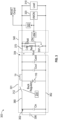
- FIG. 1 shows an example of a generic buck converter 100.
- This converter 100 will be used to show certain elements and to explain certain shortcomings thereof that embodiments disclosed herein may improve.
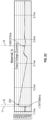
- the discussion of FIG. 1 may be aided by additional reference to FIGs. 2A-2C which show, respectively, load current during a reset of the load, current through the inductor Ls of the buck converter 100 and the output voltage of the buck converter 100.
- the buck converter 100 includes DC input 102 and that receives an input voltage from a DC voltage source 106.
- the buck converter 100 includes an input capacitor Cin across the DC input 102 that smooths the input voltage received from the DC voltage source 106.
- the converter 100 provides a stepped down DC voltage that is lower than the input voltage at its output 104.
- the voltage can be provided to a load 110 such as a digital signal processor (DSP) or a controller that, in one embodiment, can be an FPGA.
- DSP digital signal processor
- the converter 100 can also be a single monolithic IC. Eg(LT8620)
- the converter 100 also includes an output capacitor Cout across the output 104 to smooth the output.
- a switch 112 is connected between the DC input 102 and the inductor Ls.
- the inductor Ls is an energy storage element that is selectively switched into and out of electrical contract with the DC input 102 by the switch 112.
- a controller 114 can be provided to control the switch 112 and based on the duty cycle of the switch, control how much the converter 100 steps down voltage at the output 104 (Vout) from the voltage received at the DC input 102 (e.g., the voltage provided by voltage source 106).
- a control element 116 such as a diode as illustrated or another transistor
- the load 110 can require accurate voltage be provided to it.
- a voltage monitor (VMON) 120 can be provided to monitor the output voltage Vout provide to the load. If the voltage is too high above or too far below a set threshold the monitor can indicate that an abnormal condition has occurred.
- an alarm or "glitch” filter 122 can be provided. This filter is shown as an independent element but can be part of the voltage monitor 120 in some cases.
- the alarm filter 122 may require that the "alarm condition" (e.g., VMON 120 provides a positive or alarm output indication) remain for a period of time before an alarm is recognized as an actual alarm as opposed to an anomaly or a momentary voltage fluctuation that resolves in a timely manner such that the load does not need to be reset.
- the "alarm condition" e.g., VMON 120 provides a positive or alarm output indication
- the converter 100 can experience extreme load transients conditions. These conditions can make it difficult for the converter 100 to maintain its output voltage (e.g, to avoid tripping the voltage monitor 120) under the following extreme load transient scenarios:
- the buck converter 100 can be modified to respond faster by using higher switching frequency (e.g., per controller 114) and using additional bulk capacitance at the output 104.
- the additional capacitance (Cadd in FIG. 1 ) is in addition to the output capacitance Cout and in connected across the output 104. Cadd is not typically present in prior art buck converters.
- the larger output capacitance (Cadd) added to handle sudden demand in load under condition (a) type implies that large energy is stored in the output capacitor.
- condition (b) type transient when the load is suddenly removed (e.g., the load goes into reset), additional stored energy will take more time to discharge. This causes an initial overshoot and results in much larger settling time (greater than glitch time).
- the voltage monitor 120 can be any type of circuit that can monitor over and under voltage rail voltages (e.g, Vout) and provide indication whether they are within the allowable voltage levels or not.
- the monitor may generate nuisance trips/incorrect indication that buck converter is faulty which is not acceptable in safety critical applications.
- FIGs. 2A-2C which show various currents/voltages over time, as the load 110 enters reset.
- the current drawn by the load 110 drops from an normal operating value (in this case, about 500mA) to a nominal/almost zero level at time t1.
- the current through the inductor Ls sees a dramatic drop. This drop is not quit as fast as the current drop across the load and smooths out at a time t2.
- t2-t1 can be about 0.1ms but that is just an example.
- the voltage across the output (Vout) has an initial rise (see peak 202) that decays as capacitors Cout and Cadd discharge through the load.
- Vout does not get back to stable output until t3 (about 1.3ms after t2). This time, however, can result in faulty or nuisance trips as the time may be longer than that of the alarm filter 122.
- the circuit 300 includes a buck converter 301 as shown in FIG. 3 .
- the buck converter 301 includes the same elements as that of FIG. 1 and includes further elements. It should be noted that the buck converter 301 can be modified from the exact circuit shown in FIGs. 1 / 3 as long as it provides a constant stepped down output voltage.
- the diodes 116/316 could be replaced by a transistor or other type of current flow control device.
- the circuit 300 can be connected to a DC voltage source and load (and other elements) to form a system as shown in FIG. 3 .
- the circuit 300 may have reduced the settling time under "condition (b)" type load transient, so that incorrect fault indication is avoided in safety critical applications. This may allow for a simple buck regulator/converter to be used in safety critical applications where a fault has to be indicated quickly and correctly under "condition (b)" type load transient conditions.
- the circuit 300 includes a buck converter 301 and a selectively connectable transient suppression circuit 340.
- the buck converter 301 can be as above or may be modified. While describe in greater detail below, the suppression circuit 340 is connected between the DC output 304 of the buck converter and the load 310.
- the suppression circuit 340 is an R/C circuit in one embodiment and is selectively connected into the circuit 300 (e.g., to the DC output 304 of the buck converter 301) by a control switch SW1 when a "condition (b)" type transient occurs.
- the suppression circuit 340 may reduce the overshoot and/or settling time across the output (Vout) and is connected for fixed duration. This duration can be selected based on the switching speed of the buck converter 301.
- the circuit 300 includes a DC input 302 that is configured to receive an input voltage from a DC voltage source 306.
- a DC voltage source 306 Any DC voltage source discussed herein can be any source of a DC voltage such as, for example, a battery, a fly back converter, or DC rails to name but few.
- the buck converter 301 shares this DC input 302 and, thus, is also configured to receive this a voltage across the DC input 302 and does so in operation.
- the buck converter 301 includes an input capacitor Cin across the DC input 302 that smooths the input voltage received from the DC voltage source 306.
- the circuit is shown as having a positive rail 360 and neutral rail 362 that are fed by the DC voltage source 306 and define the DC input 302.
- the converter 301 provides a stepped down DC voltage (Vout) at its DC output 304 that is lower than the voltage provided by DC voltage source 306.
- the voltage can be provided to a load 310 such as a digital signal processor (DSP) or a controller that, in one embodiment, can be an FPGA.
- the converter 301 also includes an output capacitor Cout across the DC output 304 to smooth the output.
- the converter 301 can also be a single monolithic IC, eg LT8620.
- Other portions of the system of FIG. 3 can also be included in the same or a different IC including but not limited to, the selectively connectable transient suppression circuit, the dissipation circuit, and the suppression circuit switch are included in the integrated circuit all mentioned below.
- An inductor Ls is connected between the DC input 302 and the DC output 304 as in a conventional buck converter.
- a control switch 312 is connected between the DC input 302 on the positive rail 360 and the inductor Ls.
- the inductor Ls is an energy storage element that is selectively switched into and out of electrical contact with the DC input 302 by the control switch 312. It is understood that a controller 314 can be provided to control the control switch 312 and based on the duty cycle of the switch, control how much the converter 301 steps down voltage at the DC output 304 (Vout) from the voltage received at the DC input 302 (e.g, the voltage provided by the DC voltage source 306).
- a control element 116 (such as a diode as illustrated or another device such as transistor) can be connected between the rails 360 and 362, to control the direction of current flow from the inductor Ls when Ls is disconnected from the DC voltage source 306.
- a voltage monitor (VMON) 320 can be provided to monitor the output voltage Vout provided to the load 310. If the voltage is too high (e.g., above threshold) or too low the VMON 320 can indicate that an abnormal condition has occurred. That is, the VMON 320 can provide an output that is based on the DC output 304.
- an alarm or glitch filter 322 can be provided. This filter is shown as an independent element but can be part of the voltage monitor 320 in some cases.
- the alarm filter 322 may require that the "alarm condition" (e.g., VMON 320 provides a positive or alarm output indication) remain for a period of time before an alarm is recognized as an actual alarm as opposed to an anomaly or a momentary voltage fluctuation that resolves in a timely manner such that the load does not need to be reset.
- the buck converter 301 can includes additional bulk capacitance at the DC output 304.
- the additional capacitance (Cadd in FIG. 3 ) is in addition to the output capacitance Cout and in connected across the DC output 304.
- the selectively connectable transient suppression circuit 340 (suppression circuit for short).
- the suppression circuit 340 can be electrically connected into the circuit 300 in the event of reset of the load 310 in one embodiment.
- the suppression circuit 340 is connected in parallel with the DC output 304 and the load 310/VMON 320. As shown, the suppression circuit 340 is connected between the DC output 304 and the load 310. The exact location is, however, not so limited unless expressly stated in the claims below.
- the selectively connectable transient suppression circuit 340 includes a trigger 342 that is connected to the output of the VMON 320. That is, it is connected, in one embodiment, to the same signal provided to the alarm filter 322. In operation, the trigger 342 will "hold” (on its output) the signal it receives at its input for specific amount to time. In this manner, the trigger 342 can be a mono-shot element/circuit. In one embodiment, the trigger 342 is a monostable multi-vibrator implemented either using IC based solution or discrete solution, which detects rising edge/ falling edge based on the output of the VMON 320 and provides an ON output for a fixed duration.
- the output of the trigger 342 is connected to a switch (SW1) and controls whether SW1 is conductive or non-conductive.
- the fixed duration that the trigger 342 forces SW1 into the conductive (or ON) state is related to the switch frequency provided to the control switch 312 by the controller 314. In one embodiment, the duration is about 30 switching cycles (e.g., 30x the period of the signal provided to the control switch 312. While the switch SW1 is conductive, the suppression circuit 340 is electrically connected across the output DC 304 and when the switch SW1 non-conductive, the suppression circuit 340 in not electrically connected across the output DC 304 and is thereby effectively electrically removed from the circuit.
- the switch SW1 can also be called a suppression circuit control switch.
- the suppression circuit 340 also includes a dissipation circuit 370.
- the dissipation circuit is an RC circuit that includes charge capacitor Cchg serially connected to a current limiting resistor Rser.
- Cchg and Rser are serially connected between the positive rail and suppression circuit control switch SW1 in FIG. 3 such that SW1 controls current flow through Cchg and Rser.
- SW1 is closed charge balancing occurs between Cadd and Cchg resulting in overshoot limited to much smaller voltage that shown above and much faster settling time.
- Rser serves limit current through Cchg.
- the dissipation circuit 370 also includes a dissipation resistor Radd connected in parallel the serially connected Cchg and Rser to discharge the capacitor Cchg after SW1 is in the returned to the non-conductive state (e.g., after the trigger 342 expired).
- selectively connectable transient suppression circuit 340 is configured such that the suppression circuit switch SW1 is configured to electrically connect the dissipation circuit 370 to the DC output 304 when the VMON 320 determines that the voltage across the DC output 304 is above a threshold (e.g., is out of range).
- the suppression circuit switch SW1 can electrically disconnect the dissipation circuit 370 from the DC output 304 when the VMON 320 determines that the voltage across the DC output 304 is below the threshold and that the trigger 322 time has expired.
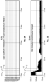
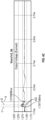
- FIGs. 4A-4C shown a simulation of the circuit 300 during a condition (b)" event.
- FIGs. 4A-4C show various currents/voltages over time as the load 310 enters reset.
- the current drawn by the load 310 drops from a normal operating value (in this case, about 500mA) to a nominal/almost zero level at time t1.
- the current through the inductor Ls FIG. 4B ) sees a dramatic drop.
- FIG. 4C shows the voltage across the output (Vout) and has an initial rise (see peak 402) that decays as capacitors Cout and Cadd discharge through the load and into Cchg (e.g, charge balancing). In the example shown, Vouts get back to stable output at t3.
- adding the additional capacitance Cchg allows for charge balancing between it and Cout/Cadd reducing in lower overshoot (e.g., peak 402 is lower than peak 202 of FIG 2C ). Further, this additional capacitance can reduce settling time bringing t3 much closer to t1 than in the prior circuit (e.g., less than 0.2 ms in the simulations of FIGs. 4A-4C ).
- circuit 300 e.g., a buck convert 301 in combination with the suppression circuit 340
- circuit 300 can provide one or more of advantages. These can include in some embodiments one or more of Very fast settling time ( ⁇ 8x improvement); Reduced overshoot ( ⁇ 2x improvement); No continuous power dissipation due to dummy load addition; Low power dissipation and high power density for a given regulator design and Simplicity of implementation due to easy scaling to different output voltage levels. to implement.
Landscapes
- Engineering & Computer Science (AREA)
- Power Engineering (AREA)
- Dc-Dc Converters (AREA)
Abstract
Description
- This application claims the benefit of
Indian Application No. 202211030945 filed May 30, 2022 - Exemplary embodiments of the present disclosure pertain to the art of power converters and, in particular, to buck converters that having low overshoot and settling time.
- Switched mode DC to DC converter power supplies are widely used to convert power from a source, such as mains power, to DC power supply for electronic devices.
- Modern embedded control systems (e.g., a field programmable gate array -FPGA or other core such as DSP core) require voltage as low as 1V DC. In aerospace or in any domain a typical standard voltage available is 28V (or 48V). So for point of load (PoL) an efficient DC-DC converter is needed to step-down the 28V (or 48V) to 1V. Further, such devices can require accurate voltage (e.g, within 5%) always be provided.
- One way to provide such power is through a buck converter. A buck converter is also referred to as step-down converter and is a DC-DC converter that reduces an input voltage to a lower, output voltage. A buck converter is in a class of converters called switched mode power supplies due the inclusion of a switching transistor that selectively provides a voltage from the input across and inductor. Such converters are small and lightweight but as further shown below, in certain situations modification of the standard circuit may be desired.
- Disclosed is a power converter for providing power to a load. The power converter includes a buck converter having a DC input and a DC output and that is configured to receive a DC voltage at the DC voltage input and provide DC output voltage at the DC output and a voltage monitor that monitors a voltage provided at the DC output. The power converter also includes a selectively connectable transient suppression circuit connected across that DC output and connected to the voltage monitor. The selectively connectable transient suppression circuit includes a dissipation circuit and a suppression circuit switch connected in series with the dissipation circuit that controls charge dissipation from the DC output into the dissipation circuit based on the voltage monitor determining that the voltage across the DC output is above a threshold.
- In embodiments, the selectively connectable transient suppression circuit is configured such that the suppression circuit switch is configured to electrically connect the dissipation circuit to the DC output when the voltage monitor determines that the voltage across the DC output is above the threshold.
- In embodiments, the selectively connectable transient suppression circuit is configured such that suppression circuit switch is configured to electrically disconnect the dissipation circuit to the DC output when the voltage monitor determines that the voltage across the DC output is below the threshold and after a time period has elapsed.
- In embodiments, the selectively connectable transient suppression circuit further includes: a trigger connected to the voltage monitor and the suppression circuit switch that controls operation of the suppression circuit switch.
- In embodiments, the trigger is monoshot circuit that holds an input signal at its output for the time period.
- In embodiments, the trigger is a monostable multi-vibrator and the time period is multiple of a switching frequency of the buck converter.
- In embodiments, the dissipation circuit includes: a charge capacitor; a current limiting resistor connected in series with charge capacitor; and a dissipation resistor connected in parallel with the series connection of the charge capacitor and the current limiting resistor.
- In embodiments, the buck converter includes: an inductor connected between the DC input and the DC output; a control switch connected between the DC input and inductor that control current flow to the inductor; and a controller that opens and closes the control switch with a signal based on the switching frequency.
- In embodiments, the time period is 30 times a period of the signal.
- In embodiments, the buck converter is included in an integrated circuit.
- In embodiments, one or more of: the selectively connectable transient suppression circuit; the dissipation circuit; and the suppression circuit switch are included in the integrated circuit.
- Also disclosed is a system that includes a power converter of any prior embodiment. The system also includes a load connected and a DC voltage source connected to the power converter. The power converter converts voltage received from DC voltage source from a first level to a second lower level and provides it to the load.
- The following descriptions should not be considered limiting in any way. With reference to the accompanying drawings, like elements are numbered alike:
-
FIG. 1 shows an example of a buck converter connected to a load according to one embodiment; -
FIGs. 2A-2C show graphs of circuit values for the circuit ofFIG. 1 ; -
FIG. 3 shows an example of a buck converter connected to a load according to one embodiment; and -
FIGs. 4A-4C show graphs of circuit values for the circuit ofFIG. 3 . - A detailed description of one or more embodiments of the disclosed apparatus and method are presented herein by way of exemplification and not limitation with reference to the Figures.
-
FIG. 1 shows an example of ageneric buck converter 100. Thisconverter 100 will be used to show certain elements and to explain certain shortcomings thereof that embodiments disclosed herein may improve. The discussion ofFIG. 1 may be aided by additional reference toFIGs. 2A-2C which show, respectively, load current during a reset of the load, current through the inductor Ls of thebuck converter 100 and the output voltage of thebuck converter 100. - The
buck converter 100 includesDC input 102 and that receives an input voltage from aDC voltage source 106. - As illustrated, the
buck converter 100 includes an input capacitor Cin across theDC input 102 that smooths the input voltage received from theDC voltage source 106. Theconverter 100 provides a stepped down DC voltage that is lower than the input voltage at itsoutput 104. The voltage can be provided to aload 110 such as a digital signal processor (DSP) or a controller that, in one embodiment, can be an FPGA. Theconverter 100 can also be a single monolithic IC. Eg(LT8620) - The
converter 100 also includes an output capacitor Cout across theoutput 104 to smooth the output. Aswitch 112 is connected between theDC input 102 and the inductor Ls. The inductor Ls is an energy storage element that is selectively switched into and out of electrical contract with theDC input 102 by theswitch 112. It is understood that acontroller 114 can be provided to control theswitch 112 and based on the duty cycle of the switch, control how much theconverter 100 steps down voltage at the output 104 (Vout) from the voltage received at the DC input 102 (e.g., the voltage provided by voltage source 106). As in known in the art, a control element 116 (such as a diode as illustrated or another transistor) can be provided that controls a direction current flow from the inductor Ls when Ls is disconnected from thesource 106. - In certain instances, the
load 110 can require accurate voltage be provided to it. To that end, a voltage monitor (VMON) 120 can be provided to monitor the output voltage Vout provide to the load. If the voltage is too high above or too far below a set threshold the monitor can indicate that an abnormal condition has occurred. Optionally, to help reduce the chances of fast, transitory changes causes too many alarms, an alarm or "glitch"filter 122 can be provided. This filter is shown as an independent element but can be part of thevoltage monitor 120 in some cases. Thealarm filter 122 may require that the "alarm condition" (e.g., VMON 120 provides a positive or alarm output indication) remain for a period of time before an alarm is recognized as an actual alarm as opposed to an anomaly or a momentary voltage fluctuation that resolves in a timely manner such that the load does not need to be reset. - The inventors hereof have discovered that is some instances, the
converter 100 can experience extreme load transients conditions. These conditions can make it difficult for theconverter 100 to maintain its output voltage (e.g, to avoid tripping the voltage monitor 120) under the following extreme load transient scenarios: - a) Out of reset condition -
load 110 draws large surge currents 10A or higher typically within 1 usec; and - b) Going to reset condition - load suddenly stops drawing current.
- To address "condition (a)" type load transient, the
buck converter 100 can be modified to respond faster by using higher switching frequency (e.g., per controller 114) and using additional bulk capacitance at theoutput 104. The additional capacitance (Cadd inFIG. 1 ) is in addition to the output capacitance Cout and in connected across theoutput 104. Cadd is not typically present in prior art buck converters. - However, it has been discovered by the inventors hereof that the addition of the bulk capacitance Cadd may reduce performance under "condition (b)" type load transient.
- With reference now to
FIGs. 1 and2A-2C , the larger output capacitance (Cadd) added to handle sudden demand in load under condition (a) type implies that large energy is stored in the output capacitor. Hence, under condition (b) type transient, when the load is suddenly removed (e.g., the load goes into reset), additional stored energy will take more time to discharge. This causes an initial overshoot and results in much larger settling time (greater than glitch time). This causes the voltage atbuck converter output 104 to be above the over voltage trip threshold set byvoltage monitor 120. As mentioned above, the voltage monitor 120 can be any type of circuit that can monitor over and under voltage rail voltages (e.g, Vout) and provide indication whether they are within the allowable voltage levels or not. However, due to the reduced settling time caused by Cadd, the monitor may generate nuisance trips/incorrect indication that buck converter is faulty which is not acceptable in safety critical applications. - For example, consider
FIGs. 2A-2C which show various currents/voltages over time, as theload 110 enters reset. In the reset condition, the current drawn by theload 110 drops from an normal operating value (in this case, about 500mA) to a nominal/almost zero level at time t1. Also, at t1, the current through the inductor Ls sees a dramatic drop. This drop is not quit as fast as the current drop across the load and smooths out at a time t2. In this case, t2-t1 can be about 0.1ms but that is just an example. However, it is noted that inFIG. 2C the voltage across the output (Vout) has an initial rise (see peak 202) that decays as capacitors Cout and Cadd discharge through the load. In the example shown, Vout does not get back to stable output until t3 (about 1.3ms after t2). This time, however, can result in faulty or nuisance trips as the time may be longer than that of thealarm filter 122. - To mitigate this problem, traditionally designers put some additional constant load on the output rail so that output capacitors (Cout/Cadd) can discharge faster reducing the settling time or utilize a linear regulator based design. Both these options result in increased power consumption.
- To address the above noted issues related to condition b above, provided is system in the form of a
circuit 300 that provides a constant output that is a stepped down version of a voltage provide at its input. Thecircuit 300 includes abuck converter 301 as shown inFIG. 3 . Thebuck converter 301 includes the same elements as that ofFIG. 1 and includes further elements. It should be noted that thebuck converter 301 can be modified from the exact circuit shown inFIGs. 1 /3 as long as it provides a constant stepped down output voltage. For example, thediodes 116/316 could be replaced by a transistor or other type of current flow control device. It shall be understood that thecircuit 300 can be connected to a DC voltage source and load (and other elements) to form a system as shown inFIG. 3 . - The
circuit 300 may have reduced the settling time under "condition (b)" type load transient, so that incorrect fault indication is avoided in safety critical applications. This may allow for a simple buck regulator/converter to be used in safety critical applications where a fault has to be indicated quickly and correctly under "condition (b)" type load transient conditions. - The
circuit 300 includes abuck converter 301 and a selectively connectabletransient suppression circuit 340. Thebuck converter 301 can be as above or may be modified. While describe in greater detail below, thesuppression circuit 340 is connected between theDC output 304 of the buck converter and theload 310. Thesuppression circuit 340 is an R/C circuit in one embodiment and is selectively connected into the circuit 300 (e.g., to theDC output 304 of the buck converter 301) by a control switch SW1 when a "condition (b)" type transient occurs. Thesuppression circuit 340 may reduce the overshoot and/or settling time across the output (Vout) and is connected for fixed duration. This duration can be selected based on the switching speed of thebuck converter 301. - The
circuit 300 includes aDC input 302 that is configured to receive an input voltage from aDC voltage source 306. Any DC voltage source discussed herein can be any source of a DC voltage such as, for example, a battery, a fly back converter, or DC rails to name but few. - The
buck converter 301 shares this DC input 302 and, thus, is also configured to receive this a voltage across theDC input 302 and does so in operation. Thebuck converter 301 includes an input capacitor Cin across theDC input 302 that smooths the input voltage received from theDC voltage source 306. Herein, the circuit is shown as having apositive rail 360 andneutral rail 362 that are fed by theDC voltage source 306 and define theDC input 302. In operation, theconverter 301 provides a stepped down DC voltage (Vout) at itsDC output 304 that is lower than the voltage provided byDC voltage source 306. - The voltage can be provided to a
load 310 such as a digital signal processor (DSP) or a controller that, in one embodiment, can be an FPGA.Theconverter 301 also includes an output capacitor Cout across theDC output 304 to smooth the output. Theconverter 301 can also be a single monolithic IC, eg LT8620. Other portions of the system ofFIG. 3 can also be included in the same or a different IC including but not limited to, the selectively connectable transient suppression circuit, the dissipation circuit, and the suppression circuit switch are included in the integrated circuit all mentioned below. - An inductor Ls is connected between the
DC input 302 and theDC output 304 as in a conventional buck converter. Acontrol switch 312 is connected between theDC input 302 on thepositive rail 360 and the inductor Ls. The inductor Ls is an energy storage element that is selectively switched into and out of electrical contact with theDC input 302 by thecontrol switch 312. It is understood that acontroller 314 can be provided to control thecontrol switch 312 and based on the duty cycle of the switch, control how much theconverter 301 steps down voltage at the DC output 304 (Vout) from the voltage received at the DC input 302 (e.g, the voltage provided by the DC voltage source 306). As in known in the art, a control element 116 (such as a diode as illustrated or another device such as transistor) can be connected between therails DC voltage source 306. - Similar to the above, a voltage monitor (VMON) 320 can be provided to monitor the output voltage Vout provided to the
load 310. If the voltage is too high (e.g., above threshold) or too low theVMON 320 can indicate that an abnormal condition has occurred. That is, theVMON 320 can provide an output that is based on theDC output 304. - Optionally, to help reduce the chances of fast, transitory changes causes too many alarms, an alarm or
glitch filter 322 can be provided. This filter is shown as an independent element but can be part of the voltage monitor 320 in some cases. Thealarm filter 322 may require that the "alarm condition" (e.g.,VMON 320 provides a positive or alarm output indication) remain for a period of time before an alarm is recognized as an actual alarm as opposed to an anomaly or a momentary voltage fluctuation that resolves in a timely manner such that the load does not need to be reset. - As in the above example, to address "condition (a)" type load transient discussed above, the
buck converter 301 can includes additional bulk capacitance at theDC output 304. The additional capacitance (Cadd inFIG. 3 ) is in addition to the output capacitance Cout and in connected across theDC output 304. - To address the reduction long settling time introduced by Cadd, provided herein is the selectively connectable transient suppression circuit 340 (suppression circuit for short). The
suppression circuit 340 can be electrically connected into thecircuit 300 in the event of reset of theload 310 in one embodiment. - As shown, the
suppression circuit 340 is connected in parallel with theDC output 304 and theload 310/VMON 320. As shown, thesuppression circuit 340 is connected between theDC output 304 and theload 310. The exact location is, however, not so limited unless expressly stated in the claims below. - The selectively connectable
transient suppression circuit 340 includes atrigger 342 that is connected to the output of theVMON 320. That is, it is connected, in one embodiment, to the same signal provided to thealarm filter 322. In operation, thetrigger 342 will "hold" (on its output) the signal it receives at its input for specific amount to time. In this manner, thetrigger 342 can be a mono-shot element/circuit. In one embodiment, thetrigger 342 is a monostable multi-vibrator implemented either using IC based solution or discrete solution, which detects rising edge/ falling edge based on the output of theVMON 320 and provides an ON output for a fixed duration. - The output of the
trigger 342 is connected to a switch (SW1) and controls whether SW1 is conductive or non-conductive. In one embodiment, the fixed duration that thetrigger 342 forces SW1 into the conductive (or ON) state is related to the switch frequency provided to thecontrol switch 312 by thecontroller 314. In one embodiment, the duration is about 30 switching cycles (e.g., 30x the period of the signal provided to thecontrol switch 312. While the switch SW1 is conductive, thesuppression circuit 340 is electrically connected across theoutput DC 304 and when the switch SW1 non-conductive, thesuppression circuit 340 in not electrically connected across theoutput DC 304 and is thereby effectively electrically removed from the circuit. Herein, the switch SW1 can also be called a suppression circuit control switch. - The
suppression circuit 340 also includes adissipation circuit 370. The dissipation circuit is an RC circuit that includes charge capacitor Cchg serially connected to a current limiting resistor Rser. Cchg and Rser are serially connected between the positive rail and suppression circuit control switch SW1 inFIG. 3 such that SW1 controls current flow through Cchg and Rser. When SW1 is closed charge balancing occurs between Cadd and Cchg resulting in overshoot limited to much smaller voltage that shown above and much faster settling time. Rser serves limit current through Cchg. Thedissipation circuit 370 also includes a dissipation resistor Radd connected in parallel the serially connected Cchg and Rser to discharge the capacitor Cchg after SW1 is in the returned to the non-conductive state (e.g., after thetrigger 342 expired). - In this manner, wherein selectively connectable
transient suppression circuit 340 is configured such that the suppression circuit switch SW1 is configured to electrically connect thedissipation circuit 370 to theDC output 304 when theVMON 320 determines that the voltage across theDC output 304 is above a threshold (e.g., is out of range). Similarly, to disconnect, the suppression circuit switch SW1 can electrically disconnect thedissipation circuit 370 from theDC output 304 when theVMON 320 determines that the voltage across theDC output 304 is below the threshold and that thetrigger 322 time has expired. -
FIGs. 4A-4C shown a simulation of thecircuit 300 during a condition (b)" event.FIGs. 4A-4C show various currents/voltages over time as theload 310 enters reset. In the reset condition, the current drawn by the load 310 (FIG. 4A ) drops from a normal operating value (in this case, about 500mA) to a nominal/almost zero level at time t1. Also, at t1, the current through the inductor Ls (FIG. 4B ) sees a dramatic drop.FIG. 4C shows the voltage across the output (Vout) and has an initial rise (see peak 402) that decays as capacitors Cout and Cadd discharge through the load and into Cchg (e.g, charge balancing). In the example shown, Vouts get back to stable output at t3. - With further reference to
FIGs. 3 and4A-4C , as compared tobuck converter 100 above, adding the additional capacitance Cchg allows for charge balancing between it and Cout/Cadd reducing in lower overshoot (e.g., peak 402 is lower thanpeak 202 ofFIG 2C ). Further, this additional capacitance can reduce settling time bringing t3 much closer to t1 than in the prior circuit (e.g., less than 0.2 ms in the simulations ofFIGs. 4A-4C ). - Based on the above, the skilled artisan will realize that circuit 300 (e.g., a
buck convert 301 in combination with the suppression circuit 340) can provide one or more of advantages. These can include in some embodiments one or more of Very fast settling time (~ 8x improvement); Reduced overshoot (~2x improvement); No continuous power dissipation due to dummy load addition; Low power dissipation and high power density for a given regulator design and Simplicity of implementation due to easy scaling to different output voltage levels. to implement. - By way of example, in the simulation of
FIGs. 4A-4C certain component values were used. These values are listed below but are not meant as limiting:


- The term "about" is intended to include the degree of error associated with measurement of the particular quantity based upon the equipment available at the time of filing the application.
- The terminology used herein is for the purpose of describing particular embodiments only and is not intended to be limiting of the present disclosure. As used herein, the singular forms "a", "an" and "the" are intended to include the plural forms as well, unless the context clearly indicates otherwise. It will be further understood that the terms "comprises" and/or "comprising," when used in this specification, specify the presence of stated features, integers, steps, operations, elements, and/or components, but do not preclude the presence or addition of one or more other features, integers, steps, operations, element components, and/or groups thereof.
- While the present disclosure has been described with reference to an exemplary embodiment or embodiments, it will be understood by those skilled in the art that various changes may be made without departing from the scope of the invention as defined by the claims. In addition, many modifications may be made to adapt a particular situation or material to the teachings of the present disclosure without departing from the scope of the claims. Therefore, it is intended that the present disclosure not be limited to the particular embodiment disclosed as the best mode contemplated for carrying out this present disclosure, but that the present disclosure will include all embodiments falling within the scope of the claims.
Claims (12)
- A power converter for providing power to a load, the power converter comprising:a buck converter (301) having a DC input (302) and a DC output (304) and that is configured to receive a DC voltage at the DC voltage input and provide DC output voltage at the DC output;a voltage monitor (320) that monitors a voltage provided at the DC output;a selectively connectable transient suppression circuit (340) connected across that DC output and connected to the voltage monitor, the selectively connectable transient suppression circuit comprising:a dissipation circuit (370); anda suppression circuit switch (SW1) connected in series with the dissipation circuit that controls charge dissipation from the DC output into the dissipation circuit based on the voltage monitor determining that the voltage across the DC output is above a threshold.
- The power converter of claim 1, wherein selectively connectable transient suppression circuit is configured such that the suppression circuit switch is configured to electrically connect the dissipation circuit to the DC output when the voltage monitor determines that the voltage across the DC output is above the threshold.
- The power converter of claim 2, wherein the selectively connectable transient suppression circuit is configured such that suppression circuit switch is configured to electrically disconnect the dissipation circuit to the DC output when the voltage monitor determines that the voltage across the DC output is below the threshold and after a time period has elapsed.
- The power converter of claim 3, wherein the selectively connectable transient suppression circuit further includes:
a trigger (342) connected to the voltage monitor and the suppression circuit switch that controls operation of the suppression circuit switch. - The power converter of claim 4, wherein the trigger is monoshot circuit that holds an input signal at its output for the time period.
- The power converter of claim 5, wherein the trigger is a monostable multi-vibrator and the time period is multiple of a switching frequency of the buck converter.
- The power converter to claim 6, wherein the dissipation circuit includes:a charge capacitor (Cchg);a current limiting resistor (Rser)connected in series with charge capacitor; anda dissipation resistor (Radd) connected in parallel with the series connection of the charge capacitor and the current limiting resistor.
- The power converter of claim 6, wherein the buck converter includes:an inductor (Ls) connected between the DC input and the DC output;a control switch (312) connected between the DC input and inductor that controls current flow to the inductor; anda controller (314) that opens and closes the control switch with a signal based on the switching frequency.
- The power converter of claim 8, wherein the time period is 30 times a period of the signal.
- The power converter of claim 9, wherein the buck converter is included in an integrated circuit.
- The power converter of claim 10, wherein one or more of the selectively connectable transient suppression circuit; the dissipation circuit; and the suppression circuit switch are included in the integrated circuit.
- A system comprising:a load (110);a DC voltage source (106); anda power converter (300) as claimed in any preceding claim, the power converter connected to the load and the DC voltage and converting voltage received from DC voltage source from a first level to a second lower level and providing it to the load.
Applications Claiming Priority (1)
| Application Number | Priority Date | Filing Date | Title |
|---|---|---|---|
| IN202211030945 | 2022-05-30 |
Publications (1)
| Publication Number | Publication Date |
|---|---|
| EP4287481A1 true EP4287481A1 (en) | 2023-12-06 |
Family
ID=86609641
Family Applications (1)
| Application Number | Title | Priority Date | Filing Date |
|---|---|---|---|
| EP23176224.6A Pending EP4287481A1 (en) | 2022-05-30 | 2023-05-30 | Low voltage buck regulator voltage regulation with reduced overshoot and settling time |
Country Status (4)
| Country | Link |
|---|---|
| US (1) | US12261528B2 (en) |
| EP (1) | EP4287481A1 (en) |
| BR (1) | BR102023009759A2 (en) |
| CA (1) | CA3198206A1 (en) |
Families Citing this family (1)
| Publication number | Priority date | Publication date | Assignee | Title |
|---|---|---|---|---|
| CN117713549B (en) * | 2024-02-06 | 2024-06-11 | 禹创半导体(深圳)有限公司 | Step-down converter, power chip and power equipment |
Citations (2)
| Publication number | Priority date | Publication date | Assignee | Title |
|---|---|---|---|---|
| US20060012346A1 (en) * | 2004-07-19 | 2006-01-19 | Jian-Rong Huang | Overshoot suppression circuit for a voltage regulation module |
| US20190157975A1 (en) * | 2017-11-20 | 2019-05-23 | Infineon Technologies Ag | Switching converter using pulse-width modulation and current-mode control |
Family Cites Families (24)
| Publication number | Priority date | Publication date | Assignee | Title |
|---|---|---|---|---|
| US6064187A (en) | 1999-02-12 | 2000-05-16 | Analog Devices, Inc. | Voltage regulator compensation circuit and method |
| JP4440614B2 (en) * | 2003-12-05 | 2010-03-24 | フェニックス電機株式会社 | High pressure discharge lamp lighting method, lighting device, and video equipment using the lighting device |
| JP5186148B2 (en) | 2006-10-02 | 2013-04-17 | 株式会社日立製作所 | Digitally controlled switching power supply |
| US7705579B1 (en) | 2008-01-14 | 2010-04-27 | National Semiconductor Corporation | Apparatus and method for faster unloading of transient response in a synchronous buck switching regulator |
| JP5333342B2 (en) * | 2009-06-29 | 2013-11-06 | 株式会社デンソー | Semiconductor device |
| US8773172B2 (en) * | 2012-11-19 | 2014-07-08 | Infineon Technologies Ag | Driver circuit with tight control of gate voltage |
| CN104377979B (en) * | 2013-08-14 | 2018-03-16 | 南京博兰得电子科技有限公司 | Inverter and its method of supplying power to and application |
| EP2874311B1 (en) * | 2013-11-15 | 2016-07-20 | Nxp B.V. | An amplifier circuit |
| US9655175B2 (en) * | 2014-06-04 | 2017-05-16 | Cree, Inc. | Off-time control for switched mode power supplies |
| JP6544674B2 (en) * | 2015-03-02 | 2019-07-17 | パナソニックIpマネジメント株式会社 | Lighting device, headlight device and vehicle |
| KR102577493B1 (en) * | 2016-07-29 | 2023-09-11 | 엘지디스플레이 주식회사 | Organic light emitting device and its driving method |
| US10116288B2 (en) | 2017-02-07 | 2018-10-30 | Hamilton Sundstrand Corporation | Reduced overhead on digital signal processing for motor drive applications |
| US10256720B2 (en) * | 2017-03-31 | 2019-04-09 | Dialog Semiconductor (Uk) Limited | Buck-boost converter using hysteretic control |
| JP6930669B2 (en) * | 2018-11-01 | 2021-09-01 | 株式会社村田製作所 | Switching converter |
| JP2021082901A (en) * | 2019-11-15 | 2021-05-27 | ソニーセミコンダクタソリューションズ株式会社 | Image pickup device and imaging apparatus |
| US11095221B1 (en) | 2020-04-16 | 2021-08-17 | Elite Semiconductor Memory Technology Inc. | Constant on-time controller and buck regulator device using the same |
| JP7380454B2 (en) * | 2020-07-01 | 2023-11-15 | トヨタ自動車株式会社 | Control device, program, and control method |
| WO2022132976A1 (en) * | 2020-12-16 | 2022-06-23 | Frore Systems Inc. | Frequency lock in active mems cooling systems |
| US12350505B2 (en) * | 2020-12-23 | 2025-07-08 | Stryker Corporation | Defibrillators with enhanced functionality during cardiopulmonary resuscitation periods |
| JP7614632B2 (en) * | 2021-03-16 | 2025-01-16 | Mirai-Labo株式会社 | Power Supplies |
| US12074529B2 (en) * | 2022-05-05 | 2024-08-27 | Cypress Semiconductor Corporation | Voltage bus discharge for universal serial bus power delivery |
| US12143004B2 (en) * | 2022-05-24 | 2024-11-12 | Murata Manufacturing Co., Ltd. | Charging circuit for bootstrap capacitors |
| US20240239198A1 (en) * | 2023-01-12 | 2024-07-18 | Ford Global Technologies, Llc | High voltage vehicle architecture |
| US12558994B2 (en) * | 2023-01-16 | 2026-02-24 | GM Global Technology Operations LLC | Electric vehicle energy storage systems including dc-dc power converters operable in selected operating modes |
-
2022
- 2022-08-31 US US17/900,224 patent/US12261528B2/en active Active
-
2023
- 2023-04-28 CA CA3198206A patent/CA3198206A1/en active Pending
- 2023-05-19 BR BR102023009759-6A patent/BR102023009759A2/en unknown
- 2023-05-30 EP EP23176224.6A patent/EP4287481A1/en active Pending
Patent Citations (2)
| Publication number | Priority date | Publication date | Assignee | Title |
|---|---|---|---|---|
| US20060012346A1 (en) * | 2004-07-19 | 2006-01-19 | Jian-Rong Huang | Overshoot suppression circuit for a voltage regulation module |
| US20190157975A1 (en) * | 2017-11-20 | 2019-05-23 | Infineon Technologies Ag | Switching converter using pulse-width modulation and current-mode control |
Non-Patent Citations (1)
| Title |
|---|
| CESPEDES MAURICIO ET AL: "Constant-Power Load System Stabilization by Passive Damping", IEEE TRANSACTIONS ON POWER ELECTRONICS, vol. 26, no. 7, 1 July 2011 (2011-07-01), USA, pages 1832 - 1836, XP093091544, ISSN: 0885-8993, Retrieved from the Internet <URL:https://ieeexplore.ieee.org/stampPDF/getPDF.jsp?tp=&arnumber=5764841&ref=aHR0cHM6Ly9pZWVleHBsb3JlLmllZWUub3JnL3NlYXJjaC9zZWFyY2hyZXN1bHQuanNwP2FjdGlvbj1zZWFyY2gmbmV3c2VhcmNoPXRydWUmbWF0Y2hCb29sZWFuPXRydWUmcXVlcnlUZXh0PSglMjJBbGwlMjBNZXRhZGF0YSUyMjpwYXNzaXZlJTIwZGFtcGluZyklMjBBTkQlMjAoJTIyQWxsJTIwTWV> DOI: 10.1109/TPEL.2011.2151880 * |
Also Published As
| Publication number | Publication date |
|---|---|
| US20230387802A1 (en) | 2023-11-30 |
| CA3198206A1 (en) | 2023-11-30 |
| BR102023009759A2 (en) | 2023-12-12 |
| US12261528B2 (en) | 2025-03-25 |
Similar Documents
| Publication | Publication Date | Title |
|---|---|---|
| KR101109975B1 (en) | Dc high power distribution assembly | |
| EP2605355B1 (en) | Intrinsically safe energy limiting circuit | |
| US9270170B2 (en) | Voltage sag corrector using a variable duty cycle boost converter | |
| JP7470109B2 (en) | Apparatus and method for discharging a DC link capacitor, power conversion device, and vehicle | |
| CN107005082A (en) | Power supply units for self-powered intelligent electronic devices | |
| CN1992491B (en) | Power supply device, low voltage circuit breaker and low voltage AC/DC electric system | |
| US7245511B2 (en) | Resistor dropper power supply with surge protection | |
| US12261528B2 (en) | Low voltage buck regulator voltage regulation with reduced overshoot and settling time | |
| EP3159994B1 (en) | Bidirectional current limiter | |
| US11038336B1 (en) | Redundant power module and discharge circuit for improved substation device availability | |
| US7463473B2 (en) | Resonance field discharge | |
| EP4324066B1 (en) | Power supply system and method for charging a power supply system | |
| JP7396240B2 (en) | Overcurrent protection circuit | |
| EP4503362A2 (en) | Surge protection and failsafe circuit for dc-dc converter | |
| US11973341B2 (en) | Surge-immune DC input supply apparatus | |
| US20030072115A1 (en) | Ultra-wide input range power supply for circuit protection devices | |
| JP2006295994A (en) | Fault current limiter and power system using the same | |
| JP4398111B2 (en) | Parallel operation system | |
| EP4531253A1 (en) | Burst mode in-rush current control for active current limiter circuit for dc-dc converter | |
| RU2754919C1 (en) | Secondary electrical power supply path with redundancy | |
| EP4622032A1 (en) | Method for fault current limiting between solid-state circuit breakers | |
| CN111106817A (en) | Signal delay circuit | |
| CN110858712A (en) | System for protecting solid state electronic devices from over-voltage and/or under-voltage conditions | |
| CN121866693A (en) | Power plant and method for operating a power plant | |
| JP2010035255A (en) | Power conversion device |
Legal Events
| Date | Code | Title | Description |
|---|---|---|---|
| PUAI | Public reference made under article 153(3) epc to a published international application that has entered the european phase |
Free format text: ORIGINAL CODE: 0009012 |
|
| STAA | Information on the status of an ep patent application or granted ep patent |
Free format text: STATUS: THE APPLICATION HAS BEEN PUBLISHED |
|
| AK | Designated contracting states |
Kind code of ref document: A1 Designated state(s): AL AT BE BG CH CY CZ DE DK EE ES FI FR GB GR HR HU IE IS IT LI LT LU LV MC ME MK MT NL NO PL PT RO RS SE SI SK SM TR |
|
| STAA | Information on the status of an ep patent application or granted ep patent |
Free format text: STATUS: REQUEST FOR EXAMINATION WAS MADE |
|
| 17P | Request for examination filed |
Effective date: 20240606 |
|
| RBV | Designated contracting states (corrected) |
Designated state(s): AL AT BE BG CH CY CZ DE DK EE ES FI FR GB GR HR HU IE IS IT LI LT LU LV MC ME MK MT NL NO PL PT RO RS SE SI SK SM TR |