EP4287243A1 - Semiconductor structure and method for manufacturing semiconductor structure - Google Patents
Semiconductor structure and method for manufacturing semiconductor structure Download PDFInfo
- Publication number
- EP4287243A1 EP4287243A1 EP21873688.2A EP21873688A EP4287243A1 EP 4287243 A1 EP4287243 A1 EP 4287243A1 EP 21873688 A EP21873688 A EP 21873688A EP 4287243 A1 EP4287243 A1 EP 4287243A1
- Authority
- EP
- European Patent Office
- Prior art keywords
- contact pad
- conductive contact
- conductive
- connecting line
- semiconductor structure
- Prior art date
- Legal status (The legal status is an assumption and is not a legal conclusion. Google has not performed a legal analysis and makes no representation as to the accuracy of the status listed.)
- Withdrawn
Links
Images






Classifications
-
- H—ELECTRICITY
- H10—SEMICONDUCTOR DEVICES; ELECTRIC SOLID-STATE DEVICES NOT OTHERWISE PROVIDED FOR
- H10W—GENERIC PACKAGES, INTERCONNECTIONS, CONNECTORS OR OTHER CONSTRUCTIONAL DETAILS OF DEVICES COVERED BY CLASS H10
- H10W90/00—Package configurations
-
- H—ELECTRICITY
- H10—SEMICONDUCTOR DEVICES; ELECTRIC SOLID-STATE DEVICES NOT OTHERWISE PROVIDED FOR
- H10W—GENERIC PACKAGES, INTERCONNECTIONS, CONNECTORS OR OTHER CONSTRUCTIONAL DETAILS OF DEVICES COVERED BY CLASS H10
- H10W72/00—Interconnections or connectors in packages
- H10W72/071—Connecting or disconnecting
-
- H—ELECTRICITY
- H10—SEMICONDUCTOR DEVICES; ELECTRIC SOLID-STATE DEVICES NOT OTHERWISE PROVIDED FOR
- H10W—GENERIC PACKAGES, INTERCONNECTIONS, CONNECTORS OR OTHER CONSTRUCTIONAL DETAILS OF DEVICES COVERED BY CLASS H10
- H10W72/00—Interconnections or connectors in packages
- H10W72/20—Bump connectors, e.g. solder bumps or copper pillars; Dummy bumps; Thermal bumps
-
- H—ELECTRICITY
- H10—SEMICONDUCTOR DEVICES; ELECTRIC SOLID-STATE DEVICES NOT OTHERWISE PROVIDED FOR
- H10W—GENERIC PACKAGES, INTERCONNECTIONS, CONNECTORS OR OTHER CONSTRUCTIONAL DETAILS OF DEVICES COVERED BY CLASS H10
- H10W20/00—Interconnections in chips, wafers or substrates
- H10W20/20—Interconnections within wafers or substrates, e.g. through-silicon vias [TSV]
-
- H—ELECTRICITY
- H10—SEMICONDUCTOR DEVICES; ELECTRIC SOLID-STATE DEVICES NOT OTHERWISE PROVIDED FOR
- H10W—GENERIC PACKAGES, INTERCONNECTIONS, CONNECTORS OR OTHER CONSTRUCTIONAL DETAILS OF DEVICES COVERED BY CLASS H10
- H10W72/00—Interconnections or connectors in packages
- H10W72/01—Manufacture or treatment
- H10W72/012—Manufacture or treatment of bump connectors, dummy bumps or thermal bumps
-
- H—ELECTRICITY
- H10—SEMICONDUCTOR DEVICES; ELECTRIC SOLID-STATE DEVICES NOT OTHERWISE PROVIDED FOR
- H10W—GENERIC PACKAGES, INTERCONNECTIONS, CONNECTORS OR OTHER CONSTRUCTIONAL DETAILS OF DEVICES COVERED BY CLASS H10
- H10W72/00—Interconnections or connectors in packages
- H10W72/01—Manufacture or treatment
- H10W72/019—Manufacture or treatment of bond pads
- H10W72/01931—Manufacture or treatment of bond pads using blanket deposition
- H10W72/01933—Manufacture or treatment of bond pads using blanket deposition in liquid form, e.g. spin coating, spray coating or immersion coating
- H10W72/01935—Manufacture or treatment of bond pads using blanket deposition in liquid form, e.g. spin coating, spray coating or immersion coating by plating, e.g. electroless plating or electroplating
-
- H—ELECTRICITY
- H10—SEMICONDUCTOR DEVICES; ELECTRIC SOLID-STATE DEVICES NOT OTHERWISE PROVIDED FOR
- H10W—GENERIC PACKAGES, INTERCONNECTIONS, CONNECTORS OR OTHER CONSTRUCTIONAL DETAILS OF DEVICES COVERED BY CLASS H10
- H10W72/00—Interconnections or connectors in packages
- H10W72/01—Manufacture or treatment
- H10W72/019—Manufacture or treatment of bond pads
- H10W72/01931—Manufacture or treatment of bond pads using blanket deposition
- H10W72/01938—Manufacture or treatment of bond pads using blanket deposition in gaseous form, e.g. by CVD or PVD
-
- H—ELECTRICITY
- H10—SEMICONDUCTOR DEVICES; ELECTRIC SOLID-STATE DEVICES NOT OTHERWISE PROVIDED FOR
- H10W—GENERIC PACKAGES, INTERCONNECTIONS, CONNECTORS OR OTHER CONSTRUCTIONAL DETAILS OF DEVICES COVERED BY CLASS H10
- H10W72/00—Interconnections or connectors in packages
- H10W72/01—Manufacture or treatment
- H10W72/019—Manufacture or treatment of bond pads
- H10W72/01951—Changing the shapes of bond pads
- H10W72/01953—Changing the shapes of bond pads by etching
-
- H—ELECTRICITY
- H10—SEMICONDUCTOR DEVICES; ELECTRIC SOLID-STATE DEVICES NOT OTHERWISE PROVIDED FOR
- H10W—GENERIC PACKAGES, INTERCONNECTIONS, CONNECTORS OR OTHER CONSTRUCTIONAL DETAILS OF DEVICES COVERED BY CLASS H10
- H10W72/00—Interconnections or connectors in packages
- H10W72/01—Manufacture or treatment
- H10W72/0198—Manufacture or treatment batch processes
-
- H—ELECTRICITY
- H10—SEMICONDUCTOR DEVICES; ELECTRIC SOLID-STATE DEVICES NOT OTHERWISE PROVIDED FOR
- H10W—GENERIC PACKAGES, INTERCONNECTIONS, CONNECTORS OR OTHER CONSTRUCTIONAL DETAILS OF DEVICES COVERED BY CLASS H10
- H10W72/00—Interconnections or connectors in packages
- H10W72/20—Bump connectors, e.g. solder bumps or copper pillars; Dummy bumps; Thermal bumps
- H10W72/241—Dispositions, e.g. layouts
- H10W72/244—Dispositions, e.g. layouts relative to underlying supporting features, e.g. bond pads, RDLs or vias
-
- H—ELECTRICITY
- H10—SEMICONDUCTOR DEVICES; ELECTRIC SOLID-STATE DEVICES NOT OTHERWISE PROVIDED FOR
- H10W—GENERIC PACKAGES, INTERCONNECTIONS, CONNECTORS OR OTHER CONSTRUCTIONAL DETAILS OF DEVICES COVERED BY CLASS H10
- H10W72/00—Interconnections or connectors in packages
- H10W72/20—Bump connectors, e.g. solder bumps or copper pillars; Dummy bumps; Thermal bumps
- H10W72/241—Dispositions, e.g. layouts
- H10W72/247—Dispositions of multiple bumps
-
- H—ELECTRICITY
- H10—SEMICONDUCTOR DEVICES; ELECTRIC SOLID-STATE DEVICES NOT OTHERWISE PROVIDED FOR
- H10W—GENERIC PACKAGES, INTERCONNECTIONS, CONNECTORS OR OTHER CONSTRUCTIONAL DETAILS OF DEVICES COVERED BY CLASS H10
- H10W72/00—Interconnections or connectors in packages
- H10W72/90—Bond pads, in general
- H10W72/921—Structures or relative sizes of bond pads
-
- H—ELECTRICITY
- H10—SEMICONDUCTOR DEVICES; ELECTRIC SOLID-STATE DEVICES NOT OTHERWISE PROVIDED FOR
- H10W—GENERIC PACKAGES, INTERCONNECTIONS, CONNECTORS OR OTHER CONSTRUCTIONAL DETAILS OF DEVICES COVERED BY CLASS H10
- H10W72/00—Interconnections or connectors in packages
- H10W72/90—Bond pads, in general
- H10W72/921—Structures or relative sizes of bond pads
- H10W72/922—Bond pads being integral with underlying chip-level interconnections
- H10W72/9226—Bond pads being integral with underlying chip-level interconnections with via interconnections
-
- H—ELECTRICITY
- H10—SEMICONDUCTOR DEVICES; ELECTRIC SOLID-STATE DEVICES NOT OTHERWISE PROVIDED FOR
- H10W—GENERIC PACKAGES, INTERCONNECTIONS, CONNECTORS OR OTHER CONSTRUCTIONAL DETAILS OF DEVICES COVERED BY CLASS H10
- H10W72/00—Interconnections or connectors in packages
- H10W72/90—Bond pads, in general
- H10W72/921—Structures or relative sizes of bond pads
- H10W72/923—Bond pads having multiple stacked layers
-
- H—ELECTRICITY
- H10—SEMICONDUCTOR DEVICES; ELECTRIC SOLID-STATE DEVICES NOT OTHERWISE PROVIDED FOR
- H10W—GENERIC PACKAGES, INTERCONNECTIONS, CONNECTORS OR OTHER CONSTRUCTIONAL DETAILS OF DEVICES COVERED BY CLASS H10
- H10W72/00—Interconnections or connectors in packages
- H10W72/90—Bond pads, in general
- H10W72/931—Shapes of bond pads
- H10W72/932—Plan-view shape, i.e. in top view
-
- H—ELECTRICITY
- H10—SEMICONDUCTOR DEVICES; ELECTRIC SOLID-STATE DEVICES NOT OTHERWISE PROVIDED FOR
- H10W—GENERIC PACKAGES, INTERCONNECTIONS, CONNECTORS OR OTHER CONSTRUCTIONAL DETAILS OF DEVICES COVERED BY CLASS H10
- H10W72/00—Interconnections or connectors in packages
- H10W72/90—Bond pads, in general
- H10W72/941—Dispositions of bond pads
-
- H—ELECTRICITY
- H10—SEMICONDUCTOR DEVICES; ELECTRIC SOLID-STATE DEVICES NOT OTHERWISE PROVIDED FOR
- H10W—GENERIC PACKAGES, INTERCONNECTIONS, CONNECTORS OR OTHER CONSTRUCTIONAL DETAILS OF DEVICES COVERED BY CLASS H10
- H10W72/00—Interconnections or connectors in packages
- H10W72/90—Bond pads, in general
- H10W72/941—Dispositions of bond pads
- H10W72/942—Dispositions of bond pads relative to underlying supporting features, e.g. bond pads, RDLs or vias
-
- H—ELECTRICITY
- H10—SEMICONDUCTOR DEVICES; ELECTRIC SOLID-STATE DEVICES NOT OTHERWISE PROVIDED FOR
- H10W—GENERIC PACKAGES, INTERCONNECTIONS, CONNECTORS OR OTHER CONSTRUCTIONAL DETAILS OF DEVICES COVERED BY CLASS H10
- H10W72/00—Interconnections or connectors in packages
- H10W72/90—Bond pads, in general
- H10W72/951—Materials of bond pads
-
- H—ELECTRICITY
- H10—SEMICONDUCTOR DEVICES; ELECTRIC SOLID-STATE DEVICES NOT OTHERWISE PROVIDED FOR
- H10W—GENERIC PACKAGES, INTERCONNECTIONS, CONNECTORS OR OTHER CONSTRUCTIONAL DETAILS OF DEVICES COVERED BY CLASS H10
- H10W72/00—Interconnections or connectors in packages
- H10W72/90—Bond pads, in general
- H10W72/951—Materials of bond pads
- H10W72/952—Materials of bond pads comprising metals or metalloids, e.g. PbSn, Ag or Cu
-
- H—ELECTRICITY
- H10—SEMICONDUCTOR DEVICES; ELECTRIC SOLID-STATE DEVICES NOT OTHERWISE PROVIDED FOR
- H10W—GENERIC PACKAGES, INTERCONNECTIONS, CONNECTORS OR OTHER CONSTRUCTIONAL DETAILS OF DEVICES COVERED BY CLASS H10
- H10W80/00—Direct bonding of chips, wafers or substrates
- H10W80/301—Bonding techniques, e.g. hybrid bonding
- H10W80/312—Bonding techniques, e.g. hybrid bonding characterised by the direct bonding of electrically conductive pads
-
- H—ELECTRICITY
- H10—SEMICONDUCTOR DEVICES; ELECTRIC SOLID-STATE DEVICES NOT OTHERWISE PROVIDED FOR
- H10W—GENERIC PACKAGES, INTERCONNECTIONS, CONNECTORS OR OTHER CONSTRUCTIONAL DETAILS OF DEVICES COVERED BY CLASS H10
- H10W80/00—Direct bonding of chips, wafers or substrates
- H10W80/301—Bonding techniques, e.g. hybrid bonding
- H10W80/327—Bonding techniques, e.g. hybrid bonding characterised by the direct bonding of insulating parts, e.g. of silicon oxide layers
-
- H—ELECTRICITY
- H10—SEMICONDUCTOR DEVICES; ELECTRIC SOLID-STATE DEVICES NOT OTHERWISE PROVIDED FOR
- H10W—GENERIC PACKAGES, INTERCONNECTIONS, CONNECTORS OR OTHER CONSTRUCTIONAL DETAILS OF DEVICES COVERED BY CLASS H10
- H10W80/00—Direct bonding of chips, wafers or substrates
- H10W80/701—Direct bonding of chips, wafers or substrates characterised by the pads after the direct bonding
-
- H—ELECTRICITY
- H10—SEMICONDUCTOR DEVICES; ELECTRIC SOLID-STATE DEVICES NOT OTHERWISE PROVIDED FOR
- H10W—GENERIC PACKAGES, INTERCONNECTIONS, CONNECTORS OR OTHER CONSTRUCTIONAL DETAILS OF DEVICES COVERED BY CLASS H10
- H10W80/00—Direct bonding of chips, wafers or substrates
- H10W80/701—Direct bonding of chips, wafers or substrates characterised by the pads after the direct bonding
- H10W80/732—Direct bonding of chips, wafers or substrates characterised by the pads after the direct bonding having shape changed during the connecting
-
- H—ELECTRICITY
- H10—SEMICONDUCTOR DEVICES; ELECTRIC SOLID-STATE DEVICES NOT OTHERWISE PROVIDED FOR
- H10W—GENERIC PACKAGES, INTERCONNECTIONS, CONNECTORS OR OTHER CONSTRUCTIONAL DETAILS OF DEVICES COVERED BY CLASS H10
- H10W90/00—Package configurations
- H10W90/20—Configurations of stacked chips
- H10W90/297—Configurations of stacked chips characterised by the through-semiconductor vias [TSVs] in the stacked chips
-
- H—ELECTRICITY
- H10—SEMICONDUCTOR DEVICES; ELECTRIC SOLID-STATE DEVICES NOT OTHERWISE PROVIDED FOR
- H10W—GENERIC PACKAGES, INTERCONNECTIONS, CONNECTORS OR OTHER CONSTRUCTIONAL DETAILS OF DEVICES COVERED BY CLASS H10
- H10W90/00—Package configurations
- H10W90/701—Package configurations characterised by the relative positions of pads or connectors relative to package parts
- H10W90/791—Package configurations characterised by the relative positions of pads or connectors relative to package parts of direct-bonded pads
- H10W90/792—Package configurations characterised by the relative positions of pads or connectors relative to package parts of direct-bonded pads between multiple chips
Definitions
- the disclosure relates to the field of semiconductor technologies, and in particular to a semiconductor structure and a manufacturing method of the semiconductor structure.
- bonding between chips is achieved by connecting metal pads on the chips to each other.
- the problem of disconnection or short-circuit connection between two metal pads of two chips is easily caused.
- the first chip includes a first substrate, a first conductive connecting line, a first conductive contact pad, and a second conductive contact pad.
- the first conductive contact pad is spaced apart from the second conductive contact pad and both of the first conductive contact pad and the second conductive contact pad are connected to the first conductive connecting line.
- an extension direction of the first conductive contact pad 43 is consistent with an extension direction of the second conductive contact pad 44. That is, the distance between the first conductive contact pad 43 and the second conductive contact pad 44 is a fixed value.
- an extension direction of the third conductive contact pad 53 is consistent with an extension direction of the fourth conductive contact pad 54. That is, the distance between the third conductive contact pad 53 and the fourth conductive contact pad 54 is a fixed value.
- the first conductive contact pad 43 and the second conductive contact pad 44 both extend in a curve direction
- the third conductive contact pad 53 and the fourth conductive contact pad 54 both extend in a curve direction
- an angle between the first conductive contact pad 43 and the third conductive contact pad 53 may be greater than 0 degrees and less than 180 degrees, i.e., it is ensured that a staggered arrangement may occur, in this case, the contact area between the upper and lower contact pads is larger with respect to the first conductive contact pad 43 being perpendicular to the third conductive contact pad 53.
- the second support contact pad 55 is located in the second substrate 51.
- the second support contact pad 55 may be located entirely in the second substrate 51, and an upper surface thereof is flush with an upper surface of the second substrate 51, or the second support contact pad 55 may be located partially in the second substrate 51, i.e., the second support contact pad 55 protrudes from the upper surface of the second substrate 51.
- the first support contact pads 45 are arranged in pairs, and the first conductive contact pad 43 and the second conductive contact pad 44 are located between the two first support contact pads 45 in pairs. That is, the outermost two first support contact pads 45 achieve reliable protection.
- an orthographic projection of the second support contact pad 55 in a direction perpendicular to the second substrate 51 coincides with the second conductive connecting line 52. That is, at least part of the second support contact pad 55 may be located directly above the second conductive connecting line 52, but the second support contact pad 55 is spaced apart from the second conductive connecting line 52.
- an orthographic projection of the first support contact pad 45 in a direction perpendicular to the first substrate 41 does not coincide with the first conductive connecting line 42. That is, the first support contact pad 45 is located in a peripheral region of the first conductive connecting line 42.
- a lower surface of the first support contact pad 45 may be higher than an upper surface of the first conductive connecting line 42, or the lower surface of the first support contact pad 45 may be equal to the upper surface of the first conductive connecting line 42, or the lower surface of the first support contact pad 45 may be lower than the upper surface of the first conductive connecting line 42.
- first conductive contact pad 43 and the second conductive contact pad 44 may both have rectangular structures
- third conductive contact pad 53 and the fourth conductive contact pad 54 may both have rectangular structures
- the first support contact pad 45 and the second support contact pad 55 may both have rectangular structures.
- the second conductive connecting line 52, the third conductive contact pad 53, and the fourth conductive contact pad 54 may include copper (Cu), tungsten (W) and other related integrated circuit conductive materials.
- the first support contact pad 45 and the second support contact pad 55 may include copper (Cu), tungsten (W) and other related integrated circuit conductive materials.
- the first conductive contact pad 30 and the third conductive contact pad 31 both extend in a curve direction.
- the support contact pad 32 is located in the substrate 10.
- the support contact pad 32 may be located partially in the substrate 10 or may be located entirely in the substrate 10.
- an orthographic projection of the support contact pad 32 in a direction perpendicular to the substrate 10 coincides with the conductive connecting line 20. That is, at least part of the support contact pad 32 may be located directly above the conductive connecting line 20, but the support contact pad 32 is spaced apart from the conductive connecting line 20.
- an orthographic projection of the support contact pad 32 in a direction perpendicular to the substrate 10 does not coincide with the conductive connecting line 20. That is, the support contact pad 32 may be located in a peripheral region of the conductive connecting line 20, but the support contact pad 32 is spaced apart from the conductive connecting line 20. A lower surface of the support contact pad 32 may be higher than an upper surface of the conductive connecting line 20, or the lower surface of the support contact pad 32 may be equal to the upper surface of the conductive connecting line 20, or the lower surface of the support contact pad 32 may be lower than the upper surface of the conductive connecting line 20.
- both the length of the first conductive contact pad 30 and the length of the second conductive contact pad 31 are greater than the diameter of the conductive connecting line 20. That is, both ends of the first conductive contact pad 30 and both ends of the second conductive contact pad 31 may be located outside the conductive connecting line 20 and not in direct contact with the conductive connecting line 20.
- the first conductive contact pad 30, the second conductive contact pad 31, and the support contact pad 32 may include copper (Cu), tungsten (W) and other related integrated circuit conductive materials.
- At least one of the first conductive contact pad 30 and the second conductive contact pad 31 may have the same structure as the support contact pad 32.
- An embodiment of the disclosure also provides a manufacturing method of a semiconductor structure.
- the manufacturing method of the semiconductor structure includes the following operations.
- a first conductive contact pad 30 and a second conductive contact pad 31 are formed in the substrate 10.
- the first conductive contact pad 30 is connected to the conductive connecting line 20 and located above the conductive connecting line 20.
- the second conductive contact pad 31 is connected to the conductive connecting line 20 and located above the conductive connecting line 20.
- the first conductive contact pad 30 is spaced apart from the second conductive contact pad 31.
- a contact surface of the conductive connecting line 20 for connecting with other conductive structures is changed by forming a first conductive contact pad 30 and a second conductive contact pad 31 which are connected to a conductive connecting line 20 and arranging the first conductive contact pad 30 and the second conductive contact pad 31 spaced apart from each other, so that the connection reliability of the semiconductor structure is improved, and the conductive connection performance of the semiconductor structure is increased.
- the substrate 10 includes a silicon substrate and an insulating layer formed above the silicon substrate.
- An upper portion of the conductive connecting line 20 is located in the insulating layer.
- the first conductive contact pad 30 and the second conductive contact pad 31 are both formed in the insulating layer.
- An upper surface of the first conductive contact pad 30 and an upper surface of the second conductive contact pad 31 are both flush with an upper surface of the insulating layer. That is, when used for bonding two wafers, insulating layers of the two wafers are bonded, and corresponding conductive contact pads are bonded.
- the insulating layer may include silicon dioxide (SiO2), silicon oxycarbide (SiOC), silicon nitride (SiN), silicon carbonitride (SiCN), and other related integrated circuit insulating materials.
- the insulating layer includes a first insulating layer 12.
- the upper portion of the conductive connecting line 20 is located in the first insulating layer 12, as shown in FIG. 9 , a second insulating layer 13 is formed on the first insulating layer 12, and the second insulating layer 13 covers a top end of the conductive connecting line 20, as shown in FIG. 10 .
- conductive structures may be provided in the silicon substrate as well as in the insulating layer, which are not limited herein, and may be selected accordingly according to requirements in the related art.
- the first conductive contact pad 30 and the second conductive contact pad 31 are formed in the corresponding openings 11.
Landscapes
- Internal Circuitry In Semiconductor Integrated Circuit Devices (AREA)
- Engineering & Computer Science (AREA)
- Manufacturing & Machinery (AREA)
Abstract
Description
- The disclosure claims priority to
Chinese patent application No. 202110259349.7, filed on March 10, 2021 - The disclosure relates to the field of semiconductor technologies, and in particular to a semiconductor structure and a manufacturing method of the semiconductor structure.
- In the related art, bonding between chips is achieved by connecting metal pads on the chips to each other. However, due to process limitations, the problem of disconnection or short-circuit connection between two metal pads of two chips is easily caused.
- The disclosure provides a semiconductor structure and a manufacturing method of the semiconductor structure, to improve the performance of the semiconductor structure.
- According to a first aspect of the disclosure, a semiconductor structure is provided, including a first chip and a second chip.
- The first chip includes a first substrate, a first conductive connecting line, a first conductive contact pad, and a second conductive contact pad. The first conductive contact pad is spaced apart from the second conductive contact pad and both of the first conductive contact pad and the second conductive contact pad are connected to the first conductive connecting line.
- The second chip includes a second substrate, a second conductive connecting line, a third conductive contact pad, and a fourth conductive contact pad. The third conductive contact pad is spaced apart from the fourth conductive contact pad and both of the third conductive contact pad and the fourth conductive contact pad are connected to the second conductive connecting line.
- The first conductive contact pad and the second conductive contact pad are both in staggered connection with the third conductive contact pad, and the first conductive contact pad and the second conductive contact pad are both in staggered connection with the fourth conductive contact pad.
- According to a second aspect of the disclosure, a semiconductor structure is provided, including a substrate, a conductive connecting line, a first conductive contact pad and a second conductive contact pad.
- The conductive connecting line is located in the substrate.
- The first conductive contact pad is located in the substrate, connected to the conductive connecting line, and located above the conductive connecting line.
- The second conductive contact pad is located in the substrate, connected to the conductive connecting line, and located above the conductive connecting line.
- The first conductive contact pad is spaced apart from the second conductive contact pad.
- According to a third aspect of the disclosure, a manufacturing method of a semiconductor structure is provided, including the following operations.
- A substrate in which a conductive connecting line is formed is provided.
- A first conductive contact pad and a second conductive contact pad are formed in the substrate. The first conductive contact pad is connected to the conductive connecting line and located above the conductive connecting line. The second conductive contact pad is connected to the conductive connecting line and located above the conductive connecting line.
- The first conductive contact pad is spaced apart from the second conductive contact pad.
- The semiconductor structure of the disclosure includes a first chip and a second chip. A first conductive connecting line of the first chip connects a first conductive contact pad and a second conductive contact pad. A second conductive connecting line of the second chip connects a third conductive contact pad and a fourth conductive contact pad. The first conductive contact pad and the second conductive contact pad are both in staggered connection with the third conductive contact pad, and are both in staggered connection with the fourth conductive contact pad, so that a reliable electrical connection between the first conductive connecting line and the second conductive connecting line is ensured, the problem of disconnection between the first conductive connecting line and the second conductive connecting line is avoided, and the performance of the semiconductor structure is improved.
- Various objects, features, and advantages of the disclosure will become more apparent from the following detailed description of preferred implementations of the disclosure when considered in conjunction with the accompanying drawings. The drawings are merely exemplary illustrations of the disclosure and are not necessarily drawn to scale. In the drawings, like reference numerals refer to the same or similar components throughout. In the drawings:
-
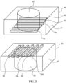
FIG. 1 is a schematic composite structure diagram of a semiconductor structure according to an exemplary implementation. -
FIG. 2 is a schematic exploded structure diagram of a semiconductor structure according to an exemplary implementation. -
FIG. 3 is a schematic cross-sectional structure diagram of a semiconductor structure according to an exemplary implementation. -
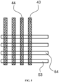
FIG. 4 is a schematic connection structure diagram of a part of a semiconductor structure according to an exemplary implementation. -
FIG. 5 is another schematic connection structure diagram of a part of a semiconductor structure according to an exemplary implementation. -
FIG. 6 is a schematic structure diagram of a semiconductor structure according to an exemplary implementation. -
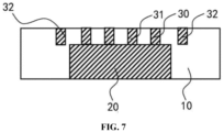
FIG. 7 is a schematic cross-sectional structure diagram of a semiconductor structure according to an exemplary implementation. -
FIG. 8 is a schematic flowchart of a manufacturing method of a semiconductor structure according to an exemplary implementation. -
FIG. 9 is a schematic structure diagram of forming a conductive connecting line in a manufacturing method of a semiconductor structure according to an exemplary implementation. -
FIG. 10 is a schematic structure diagram of forming a second insulating layer in a manufacturing method of a semiconductor structure according to an exemplary implementation. -
FIG. 11 is a schematic structure diagram of forming an opening in a manufacturing method of a semiconductor structure according to an exemplary implementation. -
FIG. 12 is a schematic structure diagram of forming a conductive contact pad in a manufacturing method of a semiconductor structure according to an exemplary implementation. - Reference numerals are illustrated as follows.
- 10, Substrate; 11, opening; 12, first insulating layer; 13, second insulating layer; 20, conductive connecting line; 30, first conductive contact pad; 31, second conductive contact pad; 32, support contact pad;
- 40, First chip; 41, first substrate; 42, first conductive connecting line; 43, first conductive contact pad; 44, second conductive contact pad; 45, first support contact pad; 50, second chip; 51, second substrate; 52, second conductive connecting line; 53, third conductive contact pad; 54, fourth conductive contact pad; 55, second support contact pad.
- Exemplary embodiments that embody the features and advantages of the disclosure will be described in detail in the following description. It will be appreciated that the disclosure may have various changes in different embodiments without departing from the scope of the disclosure, and that the description and drawings are illustrative in nature and are not intended to limit the disclosure.
- In the following description of various exemplary implementations of the disclosure, reference is made to the accompanying drawings, which form a part thereof, and in which various exemplary structures, systems, and steps capable of implementing various aspects of the disclosure are shown by way of illustration. It will be appreciated that other specific solutions of components, structures, exemplary devices, systems, and steps may be utilized and structural and functional modifications may be made without departing from the scope of the disclosure. Moreover, although the terms "on", "between", "in", etc. may be used in this specification to describe different exemplary features and elements of the disclosure, these terms are used herein for convenience only, e.g., in accordance with the orientation of the examples in the figures. Nothing in this specification should be construed as requiring a particular three-dimensional orientation of the structure to fall within the scope of the disclosure.
- An embodiment of the disclosure provides a semiconductor structure. Referring to
FIGS. 1-3 , the semiconductor structure includes afirst chip 40 and asecond chip 50. Thefirst chip 40 includes afirst substrate 41, a firstconductive connecting line 42, a firstconductive contact pad 43, and a secondconductive contact pad 44. The firstconductive contact pad 43 is spaced apart from the secondconductive contact pad 44 and both of the firstconductive contact pad 43 and the secondconductive contact pad 44 are connected to the firstconductive connecting line 42. Thesecond chip 50 includes asecond substrate 51, a second conductive connectingline 52, a thirdconductive contact pad 53, and a fourthconductive contact pad 54. The thirdconductive contact pad 53 is spaced apart from the fourthconductive contact pad 54 and both of the thirdconductive contact pad 53 and the fourthconductive contact pad 54 are connected to the secondconductive connecting line 52. The firstconductive contact pad 43 and the secondconductive contact pad 44 are both in staggered connection with the thirdconductive contact pad 53. The firstconductive contact pad 43 and the secondconductive contact pad 44 are both in staggered connection with the fourthconductive contact pad 54. - The semiconductor structure of an embodiment of the disclosure includes a
first chip 40 and asecond chip 50. A first conductive connectingline 42 of thefirst chip 40 connects a firstconductive contact pad 43 and a secondconductive contact pad 44. A second conductive connectingline 52 of thesecond chip 50 connects a thirdconductive contact pad 53 and a fourthconductive contact pad 54. The firstconductive contact pad 43 and the secondconductive contact pad 44 are both in staggered connection with the thirdconductive contact pad 53, and the firstconductive contact pad 43 and the secondconductive contact pad 44 are both in staggered connection with the fourthconductive contact pad 54, so that a reliable electrical connection between the first conductive connectingline 42 and the second conductive connectingline 52 is ensured, the problem of disconnection between the first conductive connectingline 42 and the second conductive connectingline 52 is avoided, and the performance of the semiconductor structure is improved. - It should be noted that, compared with the related art in which a conductive connecting line between an upper chip and a lower chip which are bonded connects the two chips through a large contact surface, the first
conductive contact pad 43 and the secondconductive contact pad 44 are both in staggered connection with the thirdconductive contact pad 53 and the firstconductive contact pad 43 and the secondconductive contact pad 44 are both in staggered connection with the fourthconductive contact pad 54 in the present embodiment, so that a reliable contact surface can be ensured, and a reliable electrical connection between the first conductive connectingline 42 and the second conductive connectingline 52 is ensured. - In some embodiments, the first conductive connecting
line 42, the firstconductive contact pad 43, and the secondconductive contact pad 44 are all located in thefirst substrate 41, the second conductive connectingline 52, the thirdconductive contact pad 53, and the fourthconductive contact pad 54 are all located in thesecond substrate 51, and thefirst chip 40 and thesecond chip 50 are bonded. - It should be noted that the first
conductive contact pad 43 and the secondconductive contact pad 44 may be located partially in thefirst substrate 41 or may be located entirely in thefirst substrate 41. Accordingly, the thirdconductive contact pad 53 and the fourthconductive contact pad 54 may be located partially in thesecond substrate 51 or may be located entirely in thesecond substrate 51. - In some embodiments, the first
conductive contact pad 43 and the secondconductive contact pad 44 may be located on a surface of thefirst substrate 41. Accordingly, the thirdconductive contact pad 53 and the fourthconductive contact pad 54 may be located on a surface of thesecond substrate 51. - Specifically, as shown in
FIGS. 1 and2 , thefirst chip 40 includes afirst substrate 41, a first conductive connectingline 42, a firstconductive contact pad 43, and a secondconductive contact pad 44. Thesecond chip 50 includes asecond substrate 51, a second conductive connectingline 52, a thirdconductive contact pad 53, and a fourthconductive contact pad 54. After thefirst chip 40 and thesecond chip 50 are bonded, thefirst substrate 41 and thesecond substrate 51 are bonded, and the firstconductive contact pad 43 and the secondconductive contact pad 44 are both connected to the thirdconductive contact pad 53 and the fourthconductive contact pad 54. In some cases, even if misalignment occurs, portions in contact with each other may exist, thereby ensuring a reliable electrical connection between the first conductive connectingline 42 and the second conductive connectingline 52. - In some embodiments, the first
conductive contact pad 43 and the secondconductive contact pad 44 may be identical structures. The thirdconductive contact pad 53 and the fourthconductive contact pad 54 may be identical structures. - In some embodiments, the first
conductive contact pad 43 and the secondconductive contact pad 44 may be different structures. The thirdconductive contact pad 53 and the fourthconductive contact pad 54 may be different structures. - In some embodiments, at least one of the first
conductive contact pad 43 and the secondconductive contact pad 44 may be multiple. At least one of the thirdconductive contact pad 53 and the fourthconductive contact pad 54 may be multiple. - In one embodiment, an extension direction of the first
conductive contact pad 43 is consistent with an extension direction of the secondconductive contact pad 44. That is, the distance between the firstconductive contact pad 43 and the secondconductive contact pad 44 is a fixed value. - Accordingly, an extension direction of the third
conductive contact pad 53 is consistent with an extension direction of the fourthconductive contact pad 54. That is, the distance between the thirdconductive contact pad 53 and the fourthconductive contact pad 54 is a fixed value. - In some embodiments, the first
conductive contact pad 43 and the secondconductive contact pad 44 both extend in a linear direction, and the thirdconductive contact pad 53 and the fourthconductive contact pad 54 both extend in a linear direction. - In some embodiments, the first
conductive contact pad 43 and the secondconductive contact pad 44 both extend in a curve direction, and the thirdconductive contact pad 53 and the fourthconductive contact pad 54 both extend in a curve direction. - In one embodiment, the first
conductive contact pad 43 is parallel to the secondconductive contact pad 44. That is, the firstconductive contact pad 43 and the secondconductive contact pad 44 extend in a linear direction, thereby reducing the lengths of the firstconductive contact pad 43 and the secondconductive contact pad 44. - Accordingly, the third
conductive contact pad 53 is parallel to the fourthconductive contact pad 54. That is, the thirdconductive contact pad 53 and the fourthconductive contact pad 54 extend in a linear direction, thereby reducing the lengths of the thirdconductive contact pad 53 and the fourthconductive contact pad 54. - In some embodiments, the first
conductive contact pad 43 is perpendicular to the thirdconductive contact pad 53. - Specifically, as shown in
FIG. 4 , the firstconductive contact pad 43 is parallel to the secondconductive contact pad 44, the thirdconductive contact pad 53 is parallel to the fourthconductive contact pad 54, and the firstconductive contact pad 43 is perpendicular to the thirdconductive contact pad 53. That is, the contact area between the upper and lower contact pads can be minimized, but a stable contact area can be ensured. Even if misalignment bonding occurs, that is, the bonding alignment is poor, the contact area can still be kept unchanged, and the influence on a resistance value of the contact surface is small, as shown inFIG. 5 . - In some embodiments, an angle between the first
conductive contact pad 43 and the thirdconductive contact pad 53 may be greater than 0 degrees and less than 180 degrees, i.e., it is ensured that a staggered arrangement may occur, in this case, the contact area between the upper and lower contact pads is larger with respect to the firstconductive contact pad 43 being perpendicular to the thirdconductive contact pad 53. - In one embodiment, as shown in
FIGS. 1 and2 , thefirst chip 40 further includes a firstsupport contact pad 45. The firstsupport contact pad 45 is spaced apart from the first conductive connectingline 42. The firstconductive contact pad 43 and the secondconductive contact pad 44 are both spaced apart from the firstsupport contact pad 45. Thesecond chip 50 further includes a secondsupport contact pad 55. The secondsupport contact pad 55 is spaced apart from the second conductive connectingline 52. The thirdconductive contact pad 53 and the fourthconductive contact pad 54 are both spaced apart from the secondsupport contact pad 55. The firstsupport contact pad 45 is in staggered connection with the secondsupport contact pad 55. The arrangement of the firstsupport contact pad 45 and the secondsupport contact pad 55, although electrical connection may not be achieved, can serve for support protection, thereby improving the stability and strength of the semiconductor structure. - Further, the length of the first
support contact pad 45 is greater than the diameter of the first conductive connectingline 42. That is, the firstsupport contact pad 45 is not connected to the first conductive connectingline 42, and both ends of the firstsupport contact pad 45 are located at the periphery of the first conductive connectingline 42. - Accordingly, the length of the second
support contact pad 55 is greater than the diameter of the second conductive connectingline 52. That is, the secondsupport contact pad 55 is not connected to the second conductive connectingline 52, and both ends of the secondsupport contact pad 55 are located at the periphery of the second conductive connectingline 52. - In some embodiments, the first
support contact pad 45 is located in thefirst substrate 41. The firstsupport contact pad 45 may be located entirely in thefirst substrate 41, and an upper surface thereof is flush with an upper surface of thefirst substrate 41, or the firstsupport contact pad 45 may be located partially in thefirst substrate 41, i.e., the firstsupport contact pad 45 protrudes from the upper surface of thefirst substrate 41. - Accordingly, the second
support contact pad 55 is located in thesecond substrate 51. The secondsupport contact pad 55 may be located entirely in thesecond substrate 51, and an upper surface thereof is flush with an upper surface of thesecond substrate 51, or the secondsupport contact pad 55 may be located partially in thesecond substrate 51, i.e., the secondsupport contact pad 55 protrudes from the upper surface of thesecond substrate 51. - In some embodiments, the first
support contact pad 45 is located on the upper surface of thefirst substrate 41 and the secondsupport contact pad 55 is located on the upper surface of thesecond substrate 51. - In an embodiment, the first
support contact pads 45 are arranged in pairs, and the firstconductive contact pad 43 and the secondconductive contact pad 44 are located between the two firstsupport contact pads 45 in pairs. That is, the outermost two firstsupport contact pads 45 achieve reliable protection. - Accordingly, the second
support contact pads 55 are arranged in pairs, and the thirdconductive contact pad 53 and the fourthconductive contact pad 54 are located between the two secondsupport contact pads 55 in pairs. - In some embodiments, the number of first
support contact pads 45 and the number of the secondsupport contact pads 55 may each be greater than two, which is not limited herein. - In some embodiments, an orthographic projection of the first
support contact pad 45 in a direction perpendicular to thefirst substrate 41 coincides with the first conductive connectingline 42. That is, at least part of the firstsupport contact pad 45 may be located directly above the first conductive connectingline 42, but the firstsupport contact pad 45 is spaced apart from the first conductive connectingline 42. - Accordingly, an orthographic projection of the second
support contact pad 55 in a direction perpendicular to thesecond substrate 51 coincides with the second conductive connectingline 52. That is, at least part of the secondsupport contact pad 55 may be located directly above the second conductive connectingline 52, but the secondsupport contact pad 55 is spaced apart from the second conductive connectingline 52. - In some embodiments, an orthographic projection of the first
support contact pad 45 in a direction perpendicular to thefirst substrate 41 does not coincide with the first conductive connectingline 42. That is, the firstsupport contact pad 45 is located in a peripheral region of the first conductive connectingline 42. A lower surface of the firstsupport contact pad 45 may be higher than an upper surface of the first conductive connectingline 42, or the lower surface of the firstsupport contact pad 45 may be equal to the upper surface of the first conductive connectingline 42, or the lower surface of the firstsupport contact pad 45 may be lower than the upper surface of the first conductive connectingline 42. - Accordingly, an orthographic projection of the second
support contact pad 55 in a direction perpendicular to thesecond substrate 51 does not coincide with the second conductive connectingline 52. That is, the secondsupport contact pad 55 is located in a peripheral region of the second conductive connectingline 52. A lower surface of the secondsupport contact pad 55 may be higher than an upper surface of the second conductive connectingline 52, or the lower surface of the secondsupport contact pad 55 may be equal to the upper surface of the second conductive connectingline 52, or the lower surface of the secondsupport contact pad 55 may be lower than the upper surface of the second conductive connectingline 52. - In some embodiments, the space between the first
conductive contact pad 43 and the secondconductive contact pad 44 is equal to the space between the thirdconductive contact pad 53 and the fourthconductive contact pad 54. - In some embodiments, the space between the first
conductive contact pad 43 and the secondconductive contact pad 44 is not equal to the space between the thirdconductive contact pad 53 and the fourthconductive contact pad 54, thereby ensuring that there is sufficient contact area between the contact pads of thefirst chip 40 and thesecond chip 50 even if a bond deviation occurs between thefirst chip 40 and thesecond chip 50, and avoiding the problem of disconnection. - In one embodiment, the first conductive connecting
line 42 is a first through silicon via, and the second conductive connectingline 52 is a second through silicon via. That is, the first through silicon via and the second through silicon via are connected through mutually staggered contact pads. - In some embodiments, both the length of the first
conductive contact pad 43 and the length of the secondconductive contact pad 44 are greater than the diameter of the first conductive connectingline 42. That is, both ends of the firstconductive contact pad 43 and both ends of the secondconductive contact pad 44 may be located outside the first conductive connectingline 42 and not in direct contact with the first conductive connectingline 42. - Accordingly, both the length of the third
conductive contact pad 53 and the length of the fourthconductive contact pad 54 are greater than the diameter of the second conductive connectingline 52. That is, both ends of the thirdconductive contact pad 53 and both ends of the fourthconductive contact pad 54 may be located outside the second conductive connectingline 52 and not in direct contact with the second conductive connectingline 52. - In some embodiments, the first
conductive contact pad 43 and the secondconductive contact pad 44 may both have rectangular structures, and the thirdconductive contact pad 53 and the fourthconductive contact pad 54 may both have rectangular structures. The firstsupport contact pad 45 and the secondsupport contact pad 55 may both have rectangular structures. - In some embodiments, the first conductive connecting
line 42, the firstconductive contact pad 43, and the secondconductive contact pad 44 may include copper (Cu), tungsten (W) and other related integrated circuit conductive materials. - Accordingly, the second conductive connecting
line 52, the thirdconductive contact pad 53, and the fourthconductive contact pad 54 may include copper (Cu), tungsten (W) and other related integrated circuit conductive materials. The firstsupport contact pad 45 and the secondsupport contact pad 55 may include copper (Cu), tungsten (W) and other related integrated circuit conductive materials. - In some embodiments, at least one of the first
conductive contact pad 43, the secondconductive contact pad 44, and the firstsupport contact pad 45 may have a width of 100 nm -1000 nm and a depth of 100 nm -500 nm. - At least one of the third
conductive contact pad 53, the fourthconductive contact pad 54, and the secondsupport contact pad 55 may have a width of 100 nm -1000 nm and a depth of 100 nm -500 nm. - In some embodiments, at least one of the first
conductive contact pad 43 and the secondconductive contact pad 44 may have the same structure as the firstsupport contact pad 45. At least one of the thirdconductive contact pad 53 and the fourthconductive contact pad 54 may have the same structure as the secondsupport contact pad 55. - In some embodiments, the first
conductive contact pad 43 and the secondconductive contact pad 44 may both have different structures from the firstsupport contact pad 45. The thirdconductive contact pad 53 and the fourthconductive contact pad 54 may both have different structures from the secondsupport contact pad 55. - An embodiment of the disclosure also provides a semiconductor structure. Referring to
FIGS. 6 and7 , the semiconductor structure includes: asubstrate 10; a conductive connectingline 20 located in thesubstrate 10, a firstconductive contact pad 30 located in thesubstrate 10; and a secondconductive contact pad 31 located in thesubstrate 10. The firstconductive contact pad 30 is connected to the conductive connectingline 20 and located above the conductive connectingline 20. The secondconductive contact pad 31 is connected to the conductive connectingline 20 and located above the conductive connectingline 20. The firstconductive contact pad 30 is spaced apart from the secondconductive contact pad 31. - The semiconductor structure of an embodiment of the disclosure includes a
substrate 10 and a conductive connectingline 20. A firstconductive contact pad 30 and a secondconductive contact pad 31 are connected to the conductive connectingline 20. A contact surface of the conductive connectingline 20 for connecting with other conductive structures is changed by arranging the firstconductive contact pad 30 and the secondconductive contact pad 31 spaced apart from each other, so that the connection reliability of the semiconductor structure is improved, and the conductive connection performance of the semiconductor structure is increased. - It should be noted that the first
conductive contact pad 30 is located in thesubstrate 10. The firstconductive contact pad 30 may be located partially in thesubstrate 10 or may be located entirely in thesubstrate 10. Accordingly, the secondconductive contact pad 31 may be located partially in thesubstrate 10 or may be located entirely in thesubstrate 10. - In some embodiments, the first
conductive contact pad 30 and the secondconductive contact pad 31 may be the same structures. - In some embodiments, the first
conductive contact pad 30 and the secondconductive contact pad 31 may be different structures. - In some embodiments, at least one of the first
conductive contact pad 30 and the secondconductive contact pad 31 may be multiple. - In one embodiment, an extension direction of the first
conductive contact pad 30 is consistent with an extension direction of the secondconductive contact pad 31. That is, the distance between the firstconductive contact pad 30 and the secondconductive contact pad 31 is a fixed value. - In some embodiments, the first
conductive contact pad 30 and the thirdconductive contact pad 31 both extend in a linear direction. - In some embodiments, the first
conductive contact pad 30 and the thirdconductive contact pad 31 both extend in a curve direction. - In an embodiment, the first
conductive contact pad 30 is parallel to the secondconductive contact pad 31. That is, the firstconductive contact pad 30 and the secondconductive contact pad 31 extend in a linear direction, thereby reducing the lengths of the firstconductive contact pad 30 and the secondconductive contact pad 31. - In one embodiment, as shown in
FIGS. 6 and7 , the semiconductor structure further includes asupport contact pad 32. Thesupport contact pad 32 is located in thesubstrate 10. Thesupport contact pad 32 is spaced apart from the conductive connectingline 20. The firstconductive contact pad 30 and the secondconductive contact pad 31 are both spaced apart from thesupport contact pad 32. The arrangement of thesupport contact pad 32, although electrical connection may not be achieved, can serve for support protection, thereby improving the stability and strength of the semiconductor structure. - Further, the length of the
support contact pad 32 is greater than the diameter of the conductive connectingline 20. That is, thesupport contact pad 32 is not connected to the conductive connectingline 20, and both ends of thesupport contact pad 32 are located at the periphery of the conductive connectingline 20. - In some embodiments, the
support contact pad 32 is located in thesubstrate 10. Thesupport contact pad 32 may be located partially in thesubstrate 10 or may be located entirely in thesubstrate 10. - In an embodiment, the
support contact pads 32 are arranged in pairs, and the firstconductive contact pad 30 and the secondconductive contact pad 31 are located between the twosupport contact pads 32 in pairs. That is, the outermost twosupport contact pads 32 achieve reliable protection. - In some embodiments, the number of
support contact pads 32 may be greater than two, which is not limited herein. - In some embodiments, an orthographic projection of the
support contact pad 32 in a direction perpendicular to thesubstrate 10 coincides with the conductive connectingline 20. That is, at least part of thesupport contact pad 32 may be located directly above the conductive connectingline 20, but thesupport contact pad 32 is spaced apart from the conductive connectingline 20. - In some embodiments, an orthographic projection of the
support contact pad 32 in a direction perpendicular to thesubstrate 10 does not coincide with the conductive connectingline 20. That is, thesupport contact pad 32 may be located in a peripheral region of the conductive connectingline 20, but thesupport contact pad 32 is spaced apart from the conductive connectingline 20. A lower surface of thesupport contact pad 32 may be higher than an upper surface of the conductive connectingline 20, or the lower surface of thesupport contact pad 32 may be equal to the upper surface of the conductive connectingline 20, or the lower surface of thesupport contact pad 32 may be lower than the upper surface of the conductive connectingline 20. - In an embodiment, the conductive connecting
line 20 is a through silicon via. - In some embodiments, both the length of the first
conductive contact pad 30 and the length of the secondconductive contact pad 31 are greater than the diameter of the conductive connectingline 20. That is, both ends of the firstconductive contact pad 30 and both ends of the secondconductive contact pad 31 may be located outside the conductive connectingline 20 and not in direct contact with the conductive connectingline 20. - In some embodiments, the first
conductive contact pad 30 and the secondconductive contact pad 31 may both have rectangular structures, and thesupport contact pad 32 may have a rectangular structure. - In some embodiments, the first
conductive contact pad 30, the secondconductive contact pad 31, and thesupport contact pad 32 may include copper (Cu), tungsten (W) and other related integrated circuit conductive materials. - At least one of the first
conductive contact pad 30, the secondconductive contact pad 31, and thesupport contact pad 32 may have a width of 100 nm -1000 nm and a depth of 100 nm -500 nm. - In some embodiments, at least one of the first
conductive contact pad 30 and the secondconductive contact pad 31 may have the same structure as thesupport contact pad 32. - In some embodiments, the first
conductive contact pad 30 and the secondconductive contact pad 31 may both have different structures from thesupport contact pad 32. - An embodiment of the disclosure also provides a manufacturing method of a semiconductor structure. Referring to
FIG. 8 , the manufacturing method of the semiconductor structure includes the following operations. - At S101, a
substrate 10 in which a conductive connectingline 20 is formed is provided. - At S103, a first
conductive contact pad 30 and a secondconductive contact pad 31 are formed in thesubstrate 10. The firstconductive contact pad 30 is connected to the conductive connectingline 20 and located above the conductive connectingline 20. The secondconductive contact pad 31 is connected to the conductive connectingline 20 and located above the conductive connectingline 20. - The first
conductive contact pad 30 is spaced apart from the secondconductive contact pad 31. - According to the manufacturing method of the semiconductor structure of an embodiment of the disclosure, a contact surface of the conductive connecting
line 20 for connecting with other conductive structures is changed by forming a firstconductive contact pad 30 and a secondconductive contact pad 31 which are connected to a conductive connectingline 20 and arranging the firstconductive contact pad 30 and the secondconductive contact pad 31 spaced apart from each other, so that the connection reliability of the semiconductor structure is improved, and the conductive connection performance of the semiconductor structure is increased. - In an embodiment, the
substrate 10 includes a silicon substrate and an insulating layer formed above the silicon substrate. An upper portion of the conductive connectingline 20 is located in the insulating layer. The firstconductive contact pad 30 and the secondconductive contact pad 31 are both formed in the insulating layer. An upper surface of the firstconductive contact pad 30 and an upper surface of the secondconductive contact pad 31 are both flush with an upper surface of the insulating layer. That is, when used for bonding two wafers, insulating layers of the two wafers are bonded, and corresponding conductive contact pads are bonded. - Specifically, the silicon substrate may be formed of a silicon-containing material. The silicon substrate may be formed of any suitable material, including, e.g., at least one of silicon, monocrystalline silicon, polycrystalline silicon, amorphous silicon, silicon germanium, monocrystalline silicon germanium, polycrystalline silicon germanium, and carbon-doped silicon.
- The insulating layer may include silicon dioxide (SiO2), silicon oxycarbide (SiOC), silicon nitride (SiN), silicon carbonitride (SiCN), and other related integrated circuit insulating materials.
- In some embodiments, the insulating layer includes a first insulating
layer 12. The upper portion of the conductive connectingline 20 is located in the first insulatinglayer 12, as shown inFIG. 9 , a second insulating layer 13 is formed on the first insulatinglayer 12, and the second insulating layer 13 covers a top end of the conductive connectingline 20, as shown inFIG. 10 . - It should be noted that other conductive structures may be provided in the silicon substrate as well as in the insulating layer, which are not limited herein, and may be selected accordingly according to requirements in the related art.
- In an embodiment, after multiple spaced
openings 11 are formed in the insulating layer, the firstconductive contact pad 30 and the secondconductive contact pad 31 are formed in the correspondingopenings 11. - In an embodiment, a
support contact pad 32 is formed in at least one of themultiple openings 11, and thesupport contact pad 32 is spaced apart from the conductive connectingline 20. - On the basis of
FIG. 10 , multiple spacedopenings 11 are formed in the second insulating layer 13, and theopenings 11 penetrate through the second insulating layer 13, as shown inFIG. 11 . A firstconductive contact pad 30, a secondconductive contact pad 31, and asupport contact pad 32 are then formed in themultiple openings 11, as shown inFIG. 12 . - It should be noted that the second insulating layer 13, the first
conductive contact pad 30, the secondconductive contact pad 31, and thesupport contact pad 32 may be formed by a process selected from a Physical Vapor Deposition (PVD) process, a Chemical Vapor Deposition (CVD) process, an Atomic Layer Deposition (ALD) process, an In-Situ Steam Generation (ISSG) process, a Spin On Dielectric (SOD) process, etc. The process is not limited herein. - The formation process of the
opening 11 includes photoetching, etching, etc. After each coating is formed, the coating may be treated in conjunction with a Chemical Mechanical Polishing (CMP) process to ensure the flatness of the coating. The firstconductive contact pad 30, the secondconductive contact pad 31, and thesupport contact pad 32 may be formed using a plating or sputtering process, which is not limited herein. - In an embodiment, the semiconductor structure may be formed by the above manufacturing method of the semiconductor structure.
- After considering the specification and implementing the disclosure disclosed here, other implementation solutions of the disclosure would readily be conceivable to a person skilled in the art. The disclosure is intended to cover any variations, uses, or adaptations of the disclosure following the general principles thereof and including such departures from the disclosure as come within known or customary practice in the art. It is intended that the specification and example implementations be considered as exemplary only, with a true scope and spirit of the disclosure being indicated by the foregoing claims.
- It should be understood that the disclosure is not limited to the exact construction that has been described above and illustrated in the accompanying drawings, and that various modifications and changes may be made without departing from the scope thereof. It is intended that the scope of the disclosure only be limited by the appended claims.
Claims (20)
- A semiconductor structure, comprising:a first chip, comprising a first substrate, a first conductive connecting line, a first conductive contact pad, and a second conductive contact pad, the first conductive contact pad being spaced apart from the second conductive contact pad, and both of the first conductive contact pad and the second conductive contact pad being connected to the first conductive connecting line; anda second chip, comprising a second substrate, a second conductive connecting line, a third conductive contact pad, and a fourth conductive contact pad, the third conductive contact pad being spaced apart from the fourth conductive contact pad, and both of the third conductive contact pad and the fourth conductive contact pad being connected to the second conductive connecting line,wherein the first conductive contact pad and the second conductive contact pad are both in staggered connection with the third conductive contact pad, and the first conductive contact pad and the second conductive contact pad are both in staggered connection with the fourth conductive contact pad.
- The semiconductor structure of claim 1, wherein an extension direction of the first conductive contact pad is consistent with an extension direction of the second conductive contact pad; and
an extension direction of the third conductive contact pad is consistent with an extension direction of the fourth conductive contact pad. - The semiconductor structure of claim 2, wherein the first conductive contact pad is parallel to the second conductive contact pad; and
the third conductive contact pad is parallel to the fourth conductive contact pad. - The semiconductor structure of claim 3, wherein the first conductive contact pad is perpendicular to the third conductive contact pad.
- The semiconductor structure of claim 1, wherein the first chip further comprises a first support contact pad spaced apart from the first conductive connecting line, the first conductive contact pad and the second conductive contact pad are both spaced apart from the first support contact pad;the second chip further comprises a second support contact pad spaced apart from the second conductive connecting line, the third conductive contact pad and the fourth conductive contact pad are both spaced apart from the second support contact pad; andthe first support contact pad is in staggered connection with the second support contact pad.
- The semiconductor structure of claim 5, wherein the first support contact pad is arranged in pairs, and the first conductive contact pad and the second conductive contact pad are located between two first support contact pads in pairs; and
the second support contact pad is arranged in pairs, and the third conductive contact pad and the fourth conductive contact pad are located between two second support contact pads in pairs. - The semiconductor structure of claim 5 or 6, wherein an orthographic projection of the first support contact pad in a direction perpendicular to the first substrate is not coincident with the first conductive connecting line; and
an orthographic projection of the second support contact pad in a direction perpendicular to the second substrate is not coincident with the second conductive connecting line. - The semiconductor structure of claim 1, wherein a space between the first conductive contact pad and the second conductive contact pad is not equal to a space between the third conductive contact pad and the fourth conductive contact pad.
- The semiconductor structure of claim 1, wherein the first conductive connecting line is a first through silicon via; and
the second conductive connecting line is a second through silicon via. - A semiconductor structure, comprising:a substrate;a conductive connecting line, located in the substrate;a first conductive contact pad, located in the substrate, connected to the conductive connecting line, and located above the conductive connecting line; anda second conductive contact pad, located in the substrate, connected to the conductive connecting line, and located above the conductive connecting line,wherein the first conductive contact pad is spaced apart from the second conductive contact pad.
- The semiconductor structure of claim 10, wherein an extension direction of the first conductive contact pad is consistent with an extension direction of the second conductive contact pad.
- The semiconductor structure of claim 11, wherein the first conductive contact pad is parallel to the second conductive contact pad.
- The semiconductor structure of claim 10, further comprising:a support contact pad, located in the substrate, and spaced apart from the conductive connecting line,wherein the first conductive contact pad and the second conductive contact pad are both spaced apart from the support contact pad.
- The semiconductor structure of claim 13, wherein the support contact pad is arranged in pairs, and the first conductive contact pad and the second conductive contact pad are located between two support contact pads in pairs.
- The semiconductor structure of claim 13 or 14, wherein an orthographic projection of the support contact pad in a direction perpendicular to the substrate is not coincident with the conductive connecting line.
- The semiconductor structure of claim 10, wherein the conductive connecting line is a through silicon via.
- A manufacturing method of a semiconductor structure, comprising:providing a substrate in which a conductive connecting line is formed; andforming a first conductive contact pad and a second conductive contact pad in the substrate, the first conductive contact pad being connected to the conductive connecting line and located above the conductive connecting line, and the second conductive contact pad being connected to the conductive connecting line and located above the conductive connecting line,wherein the first conductive contact pad is spaced apart from the second conductive contact pad.
- The manufacturing method of a semiconductor structure of claim 17, wherein the substrate comprises a silicon substrate and an insulating layer formed above the silicon substrate, an upper portion of the conductive connecting line is located in the insulating layer, the first conductive contact pad and the second conductive contact pad are both formed in the insulating layer, and an upper surface of the first conductive contact pad and an upper surface of the second conductive contact pad are both flush with an upper surface of the insulating layer.
- The manufacturing method of a semiconductor structure of claim 18, wherein after forming a plurality of spaced openings in the insulating layer, the first conductive contact pad and the second conductive contact pad are formed in respective openings.
- The manufacturing method of a semiconductor structure of claim 19, wherein a support contact pad is formed in at least one of the plurality of openings, the support contact pad is spaced apart from the conductive connecting line.
Applications Claiming Priority (2)
| Application Number | Priority Date | Filing Date | Title |
|---|---|---|---|
| CN202110259349.7A CN115083933A (en) | 2021-03-10 | 2021-03-10 | Semiconductor structure and manufacturing method thereof |
| PCT/CN2021/110616 WO2022188348A1 (en) | 2021-03-10 | 2021-08-04 | Semiconductor structure and method for manufacturing semiconductor structure |
Publications (2)
| Publication Number | Publication Date |
|---|---|
| EP4287243A1 true EP4287243A1 (en) | 2023-12-06 |
| EP4287243A4 EP4287243A4 (en) | 2024-08-21 |
Family
ID=83195143
Family Applications (1)
| Application Number | Title | Priority Date | Filing Date |
|---|---|---|---|
| EP21873688.2A Withdrawn EP4287243A4 (en) | 2021-03-10 | 2021-08-04 | SEMICONDUCTOR STRUCTURE AND METHOD FOR PRODUCING A SEMICONDUCTOR STRUCTURE |
Country Status (2)
| Country | Link |
|---|---|
| US (1) | US20220293542A1 (en) |
| EP (1) | EP4287243A4 (en) |
Family Cites Families (14)
| Publication number | Priority date | Publication date | Assignee | Title |
|---|---|---|---|---|
| US6642597B1 (en) * | 2002-10-16 | 2003-11-04 | Lsi Logic Corporation | Inter-layer interconnection structure for large electrical connections |
| US7968975B2 (en) * | 2008-08-08 | 2011-06-28 | International Business Machines Corporation | Metal wiring structure for integration with through substrate vias |
| US8053900B2 (en) * | 2008-10-21 | 2011-11-08 | Taiwan Semiconductor Manufacturing Company, Ltd. | Through-substrate vias (TSVs) electrically connected to a bond pad design with reduced dishing effect |
| KR102235927B1 (en) * | 2011-05-24 | 2021-04-05 | 소니 주식회사 | Semiconductor device |
| US20160093583A1 (en) * | 2014-09-25 | 2016-03-31 | Micron Technology, Inc. | Bond pad with micro-protrusions for direct metallic bonding |
| CN107615481B (en) * | 2015-05-18 | 2020-07-21 | 索尼公司 | Semiconductor device and imaging device |
| US11152417B2 (en) * | 2017-11-21 | 2021-10-19 | Taiwan Semiconductor Manufacturing Co., Ltd. | Anchor structures and methods for uniform wafer planarization and bonding |
| CN109950221A (en) * | 2019-04-15 | 2019-06-28 | 德淮半导体有限公司 | Semiconductor device and its manufacturing method |
| FR3095719A1 (en) * | 2019-05-03 | 2020-11-06 | Commissariat A L'energie Atomique Et Aux Energies Alternatives | Hybrid molecular bonding method and electronic circuit for implementing such a method |
| US11069608B2 (en) * | 2019-08-22 | 2021-07-20 | Taiwan Semiconductor Manufacturing Company, Ltd. | Semiconductor structure and manufacturing method thereof |
| US11804479B2 (en) * | 2019-09-27 | 2023-10-31 | Advanced Micro Devices, Inc. | Scheme for enabling die reuse in 3D stacked products |
| JP7378503B2 (en) * | 2019-10-12 | 2023-11-13 | 長江存儲科技有限責任公司 | Method and structure for die-to-die bonding |
| US11233088B2 (en) * | 2020-06-12 | 2022-01-25 | Omnivision Technologies, Inc. | Metal routing in image sensor using hybrid bonding |
| US11574891B2 (en) * | 2021-01-26 | 2023-02-07 | Nanya Technology Corporation | Semiconductor device with heat dissipation unit and method for fabricating the same |
-
2021
- 2021-08-04 EP EP21873688.2A patent/EP4287243A4/en not_active Withdrawn
-
2022
- 2022-02-09 US US17/650,389 patent/US20220293542A1/en not_active Abandoned
Also Published As
| Publication number | Publication date |
|---|---|
| EP4287243A4 (en) | 2024-08-21 |
| US20220293542A1 (en) | 2022-09-15 |
Similar Documents
| Publication | Publication Date | Title |
|---|---|---|
| US9793192B2 (en) | Formation of through via before contact processing | |
| KR102079283B1 (en) | Integrated circuit device having through-silicon via structure and method of manufacturing the same | |
| KR101690841B1 (en) | Stacked integrated circuits with redistribution lines | |
| CN101582407B (en) | System, structure and method of manufacturing semiconductor substrate stack | |
| US9847276B2 (en) | Semiconductor devices having through-electrodes and methods for fabricating the same | |
| CN101593743B (en) | Integrated circuit element | |
| CN114944376A (en) | Conductive barrier direct hybrid bonding | |
| WO2002089197A1 (en) | Method for bonding wafers to produce stacked integrated circuits | |
| US20180247762A1 (en) | Method of manufacturing a vertical inductor | |
| WO2017171760A1 (en) | Self-aligned via below subtractively patterned interconnect | |
| US20120098106A1 (en) | Semiconductor device and method of manufacturing the same | |
| TWI793522B (en) | Semiconductor device and method of forming the same | |
| WO2023070860A1 (en) | Semiconductor structure and forming method therefor, and wafer bonding method | |
| TW201735306A (en) | Semiconductor structure and method of manufacturing same | |
| US7268434B2 (en) | Semiconductor device and method of manufacturing the same | |
| TWI707401B (en) | Fully aligned via in ground rule region | |
| US20210287984A1 (en) | On integrated circuit (ic) device capacitor between metal lines | |
| US20090002114A1 (en) | Integrated inductor | |
| US9786426B2 (en) | Component arrangement | |
| US12482746B2 (en) | Early backside first power delivery network | |
| US20220293542A1 (en) | Semiconductor structure and manufacturing method of semiconductor structure | |
| US10170397B2 (en) | Semiconductor devices, via structures and methods for forming the same | |
| CN120380598A (en) | Semiconductor structure with backside metallization layer | |
| CN115083933A (en) | Semiconductor structure and manufacturing method thereof | |
| US20220165618A1 (en) | 3d bonded semiconductor device and method of forming the same |
Legal Events
| Date | Code | Title | Description |
|---|---|---|---|
| STAA | Information on the status of an ep patent application or granted ep patent |
Free format text: STATUS: UNKNOWN |
|
| STAA | Information on the status of an ep patent application or granted ep patent |
Free format text: STATUS: THE INTERNATIONAL PUBLICATION HAS BEEN MADE |
|
| PUAI | Public reference made under article 153(3) epc to a published international application that has entered the european phase |
Free format text: ORIGINAL CODE: 0009012 |
|
| STAA | Information on the status of an ep patent application or granted ep patent |
Free format text: STATUS: REQUEST FOR EXAMINATION WAS MADE |
|
| 17P | Request for examination filed |
Effective date: 20220405 |
|
| AK | Designated contracting states |
Kind code of ref document: A1 Designated state(s): AL AT BE BG CH CY CZ DE DK EE ES FI FR GB GR HR HU IE IS IT LI LT LU LV MC MK MT NL NO PL PT RO RS SE SI SK SM TR |
|
| DAV | Request for validation of the european patent (deleted) | ||
| DAX | Request for extension of the european patent (deleted) | ||
| A4 | Supplementary search report drawn up and despatched |
Effective date: 20240722 |
|
| RIC1 | Information provided on ipc code assigned before grant |
Ipc: H01L 25/065 20230101ALI20240716BHEP Ipc: H01L 21/98 20060101ALI20240716BHEP Ipc: H01L 21/60 20060101AFI20240716BHEP |
|
| STAA | Information on the status of an ep patent application or granted ep patent |
Free format text: STATUS: THE APPLICATION HAS BEEN WITHDRAWN |
|
| 18W | Application withdrawn |
Effective date: 20250124 |