EP4286873A1 - Open-circuit detector - Google Patents
Open-circuit detector Download PDFInfo
- Publication number
- EP4286873A1 EP4286873A1 EP23172413.9A EP23172413A EP4286873A1 EP 4286873 A1 EP4286873 A1 EP 4286873A1 EP 23172413 A EP23172413 A EP 23172413A EP 4286873 A1 EP4286873 A1 EP 4286873A1
- Authority
- EP
- European Patent Office
- Prior art keywords
- detector
- current
- voltage
- closed
- circuit
- Prior art date
- Legal status (The legal status is an assumption and is not a legal conclusion. Google has not performed a legal analysis and makes no representation as to the accuracy of the status listed.)
- Granted
Links
Images




Classifications
-
- G—PHYSICS
- G01—MEASURING; TESTING
- G01R—MEASURING ELECTRIC VARIABLES; MEASURING MAGNETIC VARIABLES
- G01R31/00—Arrangements for testing electric properties; Arrangements for locating electric faults; Arrangements for electrical testing characterised by what is being tested not provided for elsewhere
- G01R31/50—Testing of electric apparatus, lines, cables or components for short-circuits, continuity, leakage current or incorrect line connections
- G01R31/54—Testing for continuity
-
- G—PHYSICS
- G01—MEASURING; TESTING
- G01R—MEASURING ELECTRIC VARIABLES; MEASURING MAGNETIC VARIABLES
- G01R19/00—Arrangements for measuring currents or voltages or for indicating presence or sign thereof
- G01R19/165—Indicating that current or voltage is either above or below a predetermined value or within or outside a predetermined range of values
- G01R19/16533—Indicating that current or voltage is either above or below a predetermined value or within or outside a predetermined range of values characterised by the application
- G01R19/16538—Indicating that current or voltage is either above or below a predetermined value or within or outside a predetermined range of values characterised by the application in AC or DC supplies
- G01R19/16552—Indicating that current or voltage is either above or below a predetermined value or within or outside a predetermined range of values characterised by the application in AC or DC supplies in I.C. power supplies
-
- G—PHYSICS
- G01—MEASURING; TESTING
- G01R—MEASURING ELECTRIC VARIABLES; MEASURING MAGNETIC VARIABLES
- G01R31/00—Arrangements for testing electric properties; Arrangements for locating electric faults; Arrangements for electrical testing characterised by what is being tested not provided for elsewhere
- G01R31/28—Testing of electronic circuits, e.g. by signal tracer
- G01R31/2832—Specific tests of electronic circuits not provided for elsewhere
- G01R31/2836—Fault-finding or characterising
- G01R31/2843—In-circuit-testing
-
- G—PHYSICS
- G01—MEASURING; TESTING
- G01R—MEASURING ELECTRIC VARIABLES; MEASURING MAGNETIC VARIABLES
- G01R31/00—Arrangements for testing electric properties; Arrangements for locating electric faults; Arrangements for electrical testing characterised by what is being tested not provided for elsewhere
- G01R31/28—Testing of electronic circuits, e.g. by signal tracer
- G01R31/2851—Testing of integrated circuits [IC]
- G01R31/2884—Testing of integrated circuits [IC] using dedicated test connectors, test elements or test circuits on the IC under test
-
- G—PHYSICS
- G01—MEASURING; TESTING
- G01R—MEASURING ELECTRIC VARIABLES; MEASURING MAGNETIC VARIABLES
- G01R31/00—Arrangements for testing electric properties; Arrangements for locating electric faults; Arrangements for electrical testing characterised by what is being tested not provided for elsewhere
- G01R31/50—Testing of electric apparatus, lines, cables or components for short-circuits, continuity, leakage current or incorrect line connections
- G01R31/66—Testing of connections, e.g. of plugs or non-disconnectable joints
-
- G—PHYSICS
- G01—MEASURING; TESTING
- G01R—MEASURING ELECTRIC VARIABLES; MEASURING MAGNETIC VARIABLES
- G01R31/00—Arrangements for testing electric properties; Arrangements for locating electric faults; Arrangements for electrical testing characterised by what is being tested not provided for elsewhere
- G01R31/50—Testing of electric apparatus, lines, cables or components for short-circuits, continuity, leakage current or incorrect line connections
- G01R31/66—Testing of connections, e.g. of plugs or non-disconnectable joints
- G01R31/70—Testing of connections between components and printed circuit boards
- G01R31/71—Testing of solder joints
-
- G—PHYSICS
- G05—CONTROLLING; REGULATING
- G05F—SYSTEMS FOR REGULATING ELECTRIC OR MAGNETIC VARIABLES
- G05F1/00—Automatic systems in which deviations of an electric quantity from one or more predetermined values are detected at the output of the system and fed back to a device within the system to restore the detected quantity to its predetermined value or values, i.e. retroactive systems
- G05F1/10—Regulating voltage or current
- G05F1/625—Regulating voltage or current wherein it is irrelevant whether the variable actually regulated is AC or DC
Definitions
- the present specification relates to systems, methods, apparatuses, devices, articles of manufacture and instructions for open-circuit detection.
- an open-circuit detector comprising: a first current source configured to inject a current at an output of a closed-loop circuit; a detector configured to monitor a voltage of the closed-loop circuit; wherein the detector is configured to indicate whether the voltage monitored exceeds a predetermined threshold voltage; a controller configured to regulate the current injected by the first current source; wherein the controller is configured to set an open-circuit flag if the current injected caused the voltage to exceed the predetermined threshold voltage.
- the controller is configured to set the open-circuit flag if the voltage exceeded the predetermined threshold voltage within a predetermined time after the current was injected.
- the voltage monitored by the detector is at a regulated output of the closed-loop circuit.
- the voltage monitored by the detector is at a node internal to the closed-loop circuit.
- the controller is configured to cause the first current source to inject the current while the closed-loop circuit is operating.
- the controller is configured to cause the first current source to inject the current at multiple intervals after the closed-loop circuit starts operating and before the closed-loop circuit stops operating.
- the controller is configured to adjust an amplitude or duration of the current injected by the first current source based on a load current drawn at the output of the closed-loop circuit.
- a current drain coupled between the output and a ground; wherein the controller is configured to adjust an amount of a current drained by the current drain based on a discharge time of an external load capacitor coupled to the output.
- the output of the closed-loop circuit is configured to be coupled an external capacitor configured to keep the output voltage within a predetermined ripple voltage range; and the current injected by the current source does not cause the output voltage to exceed the predetermined ripple voltage range.
- the closed-loop circuit is a voltage regulator including an output driver and a compensation capacitor; the compensation capacitor is coupled to a gate of the output driver; further comprising a second current source coupled in parallel with the first current source; wherein the controller is configured to adjust a duration or amplitude of the current injected by the second current source based on a value of the compensation capacitor.
- the closed-loop circuit is a voltage regulator.
- the voltage regulator is a low drop out (LDO) regulator.
- LDO low drop out
- the current is a pull up current injected at an output lead of the voltage regulator.
- the open-circuit detector is embedded within an integrated circuit.
- the detector is coupled to monitor the voltage at an output pin of a chip package.
- the detector is coupled to monitor the voltage at a wire bond between an integrated circuit die and a lead-frame within a chip package.
- the voltage monitored by the detector is at an output of an operational amplifier internal to the closed-loop circuit.
- an open-circuit detector comprising: a current source configured to inject a current at an output of an open-loop circuit; a detector configured to monitor a voltage of the open-loop circuit; wherein the detector is configured to indicate whether the voltage exceeds a predetermined threshold voltage; a controller configured to regulate the current injected by the current source; wherein the controller is configured to set an open-circuit flag if the current injected caused the voltage to exceed the predetermined threshold voltage.
- Open-circuit detection within integrated circuit dies, chip packages, and between a chip package and a circuit board is often necessary for a safe shut-down of a circuit or to place a larger system into a safe-mode.
- an open-circuit detector configured to detect various pin-lift conditions in a monitored circuit.
- Such circuits may include closed-loop circuits, such as voltage regulators, LDO (low drop out) regulators, PMICs (Power Management Integrated Circuits), etc., as well as other circuits.
- the open-circuit detector is used to detect a pin-lift condition of a closed-loop circuit having a weak pull down.
- Pin-lift is herein defined as anything that would interfere with continuity (e.g. broken wire, broken wire-bond, broken integrated circuit trace, solder break, un-plugging a device, etc.), either internal to an integrated circuit, internal to a chip package, on a printed circuit board (PCB), or within an electronic system.
- continuity e.g. broken wire, broken wire-bond, broken integrated circuit trace, solder break, un-plugging a device, etc.
- PCB printed circuit board
- Example embodiments of this open-circuit detector use a current source to inject a fixed current into the monitored circuit and a detection circuit to monitor one or more nodes in the circuit.
- the current is injected periodically by a controller (e.g. state machine) and continuous monitoring is done to check for any pin-lift conditions during operation, at power up, at power down, under load, and under no load.
- a controller e.g. state machine
- the voltage developed on the output pin during the current injection is monitored by a detector circuit. If a pin-lift condition is present, the injected current will quickly pull up the pin causing the comparator to trip and flag an overvoltage at the pin. If conditions are normal, the injected current is absorbed by the load (on the pin) and no overvoltage condition is generated.
- the open-circuit detector is designed to be added onto existing voltage regulators (e.g. LDOs) and does not require any changes to the functional or parametric requirements of the voltage regulators to work. No additional pin is required for this open-circuit detector.
- existing voltage regulators e.g. LDOs
- Figure 1A represents a first example 100 of an open-circuit detector.
- the example 100 shows internal circuits 102 (e.g. IC, chip, die, etc.) and external circuits 104 (e.g. PCB, load, etc.)
- internal circuits 102 e.g. IC, chip, die, etc.
- external circuits 104 e.g. PCB, load, etc.
- the internal circuits 102 include a closed-loop circuit 106 and the open-circuit detector which includes a first current source 108, a detector 110, and a controller 112 (e.g. digital state-machine).
- the external circuits 104 in this example include an external output capacitor (Cout) and a load current (Iload).
- the closed-loop circuit 106 is a voltage regulator (e.g. LDO)
- the external output capacitor supports fast transient loads as well as provides DC stability for the voltage regulator.
- the open-circuit detector works by the controller 112 closing switch S1 and thereby injecting a current Ipu periodically at an output pin 114 of the closed-loop circuit 106 (e.g. voltage regulator). Ipu is periodically injected by the controller 112 digitally controlling the switch S1.
- Ipu is periodically injected by the controller 112 digitally controlling the switch S1.
- the detector 110 monitors a voltage at the output pin 114, and compares the voltage to a predetermined threshold voltage, which if exceeded during the Ipu current injection, sets the OV flag 116.
- the closed-loop circuit 106 can be any linear regulator (PMOS or NMOS) with the ability to source current from the supply Vin_ldo.
- the supply voltages Vin_op_amp and Vin_ldo may or may not be the same depending on the architecture of the closed-loop circuit 106 and this has no effect on the working of the open-circuit detector.
- Vin_cs is a voltage that is greater than the regulated output voltage of the voltage regulator.
- Vin_cs can be connected to a highest supply on this chip, or it can be connected to Vin_ldo. If Vin_ldo is shorted to Vin_cs the headroom requirement of current source Ipu becomes smaller. If Vin_cs is connected to a higher supply voltage, high voltage devices may be required which occupies more circuit area for the same current density.
- S1 is a switch with low Rdson digitally controlled by the controller 112.
- a timing (Tperiod) of this control is dictated by the acceptable ripple allowed on Cout and the sampling time (Ton) of the failure detection. For example for an allowed a 5mV ripple for a 3.3V/5V output with a pin-lift failure being detected within 5ms can use a Ton of 80us and Tperiod of 2ms.
- the open-circuit detector has at least two operating modes (e.g. a normal, no-fault mode and a pin-lift, fault mode.
- the injected current Ipu will either be absorbed by the load (Iload) or integrated over the external capacitor (Cout) depending on the value of the load.
- the periodically injected current Ipu causes an output ripple on the output voltage of the external capacitor. This ripple is relatively small and within the acceptable accuracy of the voltage regulator.
- Figure 1B represents an example no-fault timing diagram 120 of the first example 100 open-circuit detector. Shown is the switch S1 state having a Tperiod and Ton time when current is injected at the output pin 114. The Cout voltage is monitored by the detector 110 and is the same as the voltage at the output pin 114. An "acceptable ripple" is also shown based on an application that will not violate the application's design rules.
- V1 is the predetermined threshold voltage, which if exceeded during the Ton current injection, sets the OV flag 116.
- Tdis_chg is determined by Ileakage. Ileakage models internal resistor dividers and/or other current leakage paths that are connected to the output of closed-loop circuit 106. These resistors may provide the following functions including but not limited to output voltage detection, feedback for stability, sampling the output voltage for an ADC.
- Figure 1C represents an example fault state 130 detectable by the first example 100 open-circuit detector.
- the circuit in this example fault state 130 is the same as for example 100 except for an open-circuit (e.g. Pin Lift) event 132.
- an open-circuit e.g. Pin Lift
- Figure 1D represents a first example fault timing diagram 140 of the first open-circuit detector.
- the pin-lift event 132 occurs (see Figure 1C )
- capacitor Cout is disconnected from the closed-loop circuit 106 output.
- the current Ipu pulls the output voltage of the closed-loop circuit 106 higher than the overvoltage detection threshold after the pin-lift event 132 occurs.
- This overvoltage condition is detected by the detector 110 which then sets the OV flag 116 (e.g. indicator) after a digital filter.
- Ipu is sufficiently large to overcome the leakage current Ileakage. Note that Cout voltage decays over time due to the external load or other leakage.
- Figure 2 represents a second example 200 of the open-circuit detector.
- the second example 200 is substantially same as the first example 100 except for the addition of a current drain 202.
- the closed-loop circuit 106, first current source 108, detector 110, and controller 112 are still present in the second example 200 but are not labeled here to increase clarity.
- the second example 200 of the open-circuit detector is applicable to example embodiments where the closed-loop circuit's 106 value of Tdis_chg (see Figure 1B ) is larger than Toff (i.e. time during Tperiod not including Ton).
- capacitor Cout is not be sufficiently discharged before the next current pulse is injected. This is occurs if Ileakage is relatively small.
- the current drain 202 having a drain current Ipd and a switch S2, is added to provided to more quickly discharge Cout.
- the switch S2 is also controlled by the controller 112.
- Figure 3A represents a second example fault timing diagram 300 of the first example 100 open-circuit detector.
- Linear voltage regulators for loop stability are often compensated with an internal capacitor (Ccomp) connected to a gate of the regulators output driver (as shown in Figure 1A ).
- the value of the internal capacitor Ccomp is usually smaller than Cout by 5 to 6 orders of magnitude.
- the compensation capacitor (Ccomp) in the closed-loop circuit 106 may need to be charged up by current source Ipu . If the current Ipu if is not large enough, the compensation capacitor (Ccomp) will take longer to charge and the closed-loop circuit 106 output voltage may not trigger an overvoltage flag within Ton as shown in Figure 3A . If Ipu is simply increased to charge the internal compensation capacitor (Ccomp) faster during a fault mode, design constraints on the acceptable ripple (see Figure 1B ) during normal mode may be violated. Figure 3B shows an example solution to this concern.
- Figure 3B represents a third example 310 of the open-circuit detector.
- the third example 310 is substantially same as the first example 100 except for the addition of a second current source 312 (Icomp) and identification of an output driver 314.
- the closed-loop circuit 106, first current source 108, detector 110, and controller 112 are still present in the third example 310 but are not labeled here to increase clarity.
- the second current source 312 (Icomp) is activated by a third switch S3 by the controller 112 to overcome this issue, and is switched in parallel with the first current source 108, having the current (Ipu) and the switch (S1), to charge the compensation capacitor (Ccomp) faster for at least a part of the Ton time.
- Figure 3C represents a first example timing diagram 320 of the third example 310 open-circuit detector.
- the first example timing diagram 320 shows various waveforms for the third example 310 open-circuit detector, including showing an OV (over voltage) duration with auxiliary current injection by the second current source 312 (Icomp).
- Figure 3D represents a second example timing diagram 330 of the third example 310 open-circuit detector.
- the second example timing diagram 330 shows various waveforms for the third example 310 open-circuit detector, including showing an OV (over voltage) duration without auxiliary current injection by the second current source 312 (Icomp).
- Figure 4 represents a fourth example 400 of the open-circuit detector.
- the fourth example 400 is an example implemented version of the first example 100 of the open-circuit detector. This example implemented version is configured to detect both an overvoltage and an undervoltage at Vout. Ileakage is modelled as resistors R1-2 and R3-5.
- Figure 5 represents a fifth example 500 of the open-circuit detector.
- the fifth example 500 of the open-circuit detector includes a closed-loop circuit 502, and an open-circuit detector.
- the open-circuit detector includes a current source 504, a detector 506, and a controller 508.
- the detector 506 monitors a voltage at an output pin 510, and compares the voltage to a predetermined threshold voltage, which if exceeded during the Ipu current injection by the current source 504, sets an OV flag 512.
- An op-amp present in the closed-loop circuit 502 can be used as a comparator to detect a pin-lift event.
- a gate of the linear regulator begins to turn an output FET of the closed-loop circuit 502 off.
- the gate voltage is monitored to set the OV flag 512 (e.g. indicator).
- Transistor M1 is a PMOS with its gate tied to the gate of the output FET of the closed-loop circuit 502. The sources of M1 and the output FET are also shorted together. M1 is biased using a current source Ibias. M1 and current source Ibias essential form an internal comparator.
- a level shifter in the detector 506 is used to level shift this voltage to the digital supply before the flag is sent to the controller 508.
- An advantage of the fifth example 500 of the open-circuit detector is a conventional two input comparator is not required. However, a speed of detection depends on the gm, bias currents and internal compensation capacitors within the closed-loop circuit 106.
- these instructions/steps are implemented as functional and software instructions.
- the instructions can be implemented either using logic gates, application specific chips, firmware, as well as other hardware forms.
- the instructions are embodied as a set of executable instructions in a non-transitory computer-readable or computer-usable media which are effected on a computer or machine programmed with and controlled by said executable instructions.
- Said instructions are loaded for execution on a processor (such as one or more CPUs).
- Said processor includes microprocessors, microcontrollers, processor modules or subsystems (including one or more microprocessors or microcontrollers), or other control or computing devices.
- a processor can refer to a single component or to plural components.
- Said computer-readable or computer-usable storage medium or media is (are) considered to be part of an article (or article of manufacture).
- An article or article of manufacture can refer to any manufactured single component or multiple components.
- the non-transitory machine or computer-usable media or mediums as defined herein excludes signals, but such media or mediums may be capable of receiving and processing information from signals and/or other transitory mediums.
Landscapes
- General Physics & Mathematics (AREA)
- Physics & Mathematics (AREA)
- Engineering & Computer Science (AREA)
- Power Engineering (AREA)
- General Engineering & Computer Science (AREA)
- Automation & Control Theory (AREA)
- Electromagnetism (AREA)
- Radar, Positioning & Navigation (AREA)
- Microelectronics & Electronic Packaging (AREA)
- Computer Hardware Design (AREA)
- Dc-Dc Converters (AREA)
- Emergency Protection Circuit Devices (AREA)
- Measurement Of Current Or Voltage (AREA)
Abstract
Description
- The present specification relates to systems, methods, apparatuses, devices, articles of manufacture and instructions for open-circuit detection.
- According to an example embodiment, an open-circuit detector, comprising: a first current source configured to inject a current at an output of a closed-loop circuit; a detector configured to monitor a voltage of the closed-loop circuit; wherein the detector is configured to indicate whether the voltage monitored exceeds a predetermined threshold voltage; a controller configured to regulate the current injected by the first current source; wherein the controller is configured to set an open-circuit flag if the current injected caused the voltage to exceed the predetermined threshold voltage.
- In another example embodiment, the controller is configured to set the open-circuit flag if the voltage exceeded the predetermined threshold voltage within a predetermined time after the current was injected.
- In another example embodiment, the voltage monitored by the detector is at a regulated output of the closed-loop circuit.
- In another example embodiment, the voltage monitored by the detector is at a node internal to the closed-loop circuit.
- In another example embodiment, the controller is configured to cause the first current source to inject the current while the closed-loop circuit is operating.
- In another example embodiment, the controller is configured to cause the first current source to inject the current at multiple intervals after the closed-loop circuit starts operating and before the closed-loop circuit stops operating.
- In another example embodiment, the controller is configured to adjust an amplitude or duration of the current injected by the first current source based on a load current drawn at the output of the closed-loop circuit.
- In another example embodiment, further comprising a current drain coupled between the output and a ground; wherein the controller is configured to adjust an amount of a current drained by the current drain based on a discharge time of an external load capacitor coupled to the output.
- In another example embodiment, the output of the closed-loop circuit is configured to be coupled an external capacitor configured to keep the output voltage within a predetermined ripple voltage range; and the current injected by the current source does not cause the output voltage to exceed the predetermined ripple voltage range.
- In another example embodiment, the closed-loop circuit is a voltage regulator including an output driver and a compensation capacitor; the compensation capacitor is coupled to a gate of the output driver; further comprising a second current source coupled in parallel with the first current source; wherein the controller is configured to adjust a duration or amplitude of the current injected by the second current source based on a value of the compensation capacitor.
- In another example embodiment, the closed-loop circuit is a voltage regulator.
- In another example embodiment, the voltage regulator is a low drop out (LDO) regulator.
- In another example embodiment, the current is a pull up current injected at an output lead of the voltage regulator.
- In another example embodiment, the open-circuit detector is embedded within an integrated circuit.
- In another example embodiment, the detector is coupled to monitor the voltage at an output pin of a chip package.
- In another example embodiment, the detector is coupled to monitor the voltage at a wire bond between an integrated circuit die and a lead-frame within a chip package.
- In another example embodiment, the voltage monitored by the detector is at an output of an operational amplifier internal to the closed-loop circuit.
- According to an example embodiment, an open-circuit detector, comprising: a current source configured to inject a current at an output of an open-loop circuit; a detector configured to monitor a voltage of the open-loop circuit; wherein the detector is configured to indicate whether the voltage exceeds a predetermined threshold voltage; a controller configured to regulate the current injected by the current source; wherein the controller is configured to set an open-circuit flag if the current injected caused the voltage to exceed the predetermined threshold voltage.
- The above discussion is not intended to represent every example embodiment or every implementation within the scope of the current or future Claim sets. The Figures and Detailed Description that follow also exemplify various example embodiments.
- Various example embodiments may be more completely understood in consideration of the following Detailed Description in connection with the accompanying Drawings.
-
-
Figure 1A represents a first example of an open-circuit detector. -
Figure 1B represents an example no-fault timing diagram of the first example open-circuit detector. -
Figure 1C represents an example fault state detectable by the first example open-circuit detector. -
Figure 1D represents a first example fault timing diagram of the first example open-circuit detector. -
Figure 2 represents a second example of the open-circuit detector. -
Figure 3A represents a second example fault timing diagram of the first example open-circuit detector. -
Figure 3B represents a third example of the open-circuit detector. -
Figure 3C represents a first example timing diagram of the third example open-circuit detector. -
Figure 3D represents a second example timing diagram of the third example open-circuit detector. -
Figure 4 represents a fourth example of the open-circuit detector. -
Figure 5 represents a fifth example of the open-circuit detector. - While the disclosure is amenable to various modifications and alternative forms, specifics thereof have been shown by way of example in the drawings and will be described in detail. It should be understood, however, that other embodiments, beyond the particular embodiments described, are possible as well. All modifications, equivalents, and alternative embodiments falling within the spirit and scope of the appended claims are covered as well.
- Open-circuit detection within integrated circuit dies, chip packages, and between a chip package and a circuit board is often necessary for a safe shut-down of a circuit or to place a larger system into a safe-mode.
- Discussed herein are various example embodiments of an open-circuit detector configured to detect various pin-lift conditions in a monitored circuit. Such circuits may include closed-loop circuits, such as voltage regulators, LDO (low drop out) regulators, PMICs (Power Management Integrated Circuits), etc., as well as other circuits. In some example embodiments, the open-circuit detector is used to detect a pin-lift condition of a closed-loop circuit having a weak pull down.
- Pin-lift is herein defined as anything that would interfere with continuity (e.g. broken wire, broken wire-bond, broken integrated circuit trace, solder break, un-plugging a device, etc.), either internal to an integrated circuit, internal to a chip package, on a printed circuit board (PCB), or within an electronic system.
- Example embodiments of this open-circuit detector use a current source to inject a fixed current into the monitored circuit and a detection circuit to monitor one or more nodes in the circuit. In some example embodiments, the current is injected periodically by a controller (e.g. state machine) and continuous monitoring is done to check for any pin-lift conditions during operation, at power up, at power down, under load, and under no load.
- The voltage developed on the output pin during the current injection is monitored by a detector circuit. If a pin-lift condition is present, the injected current will quickly pull up the pin causing the comparator to trip and flag an overvoltage at the pin. If conditions are normal, the injected current is absorbed by the load (on the pin) and no overvoltage condition is generated.
- The open-circuit detector is designed to be added onto existing voltage regulators (e.g. LDOs) and does not require any changes to the functional or parametric requirements of the voltage regulators to work. No additional pin is required for this open-circuit detector.
-
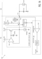
Figure 1A represents a first example 100 of an open-circuit detector. The example 100 shows internal circuits 102 (e.g. IC, chip, die, etc.) and external circuits 104 (e.g. PCB, load, etc.) - The
internal circuits 102 include a closed-loop circuit 106 and the open-circuit detector which includes a firstcurrent source 108, adetector 110, and a controller 112 (e.g. digital state-machine). Theexternal circuits 104 in this example include an external output capacitor (Cout) and a load current (Iload). For example embodiments where the closed-loop circuit 106 is a voltage regulator (e.g. LDO), the external output capacitor supports fast transient loads as well as provides DC stability for the voltage regulator. - The open-circuit detector works by the
controller 112 closing switch S1 and thereby injecting a current Ipu periodically at anoutput pin 114 of the closed-loop circuit 106 (e.g. voltage regulator). Ipu is periodically injected by thecontroller 112 digitally controlling the switch S1. - The
detector 110 monitors a voltage at theoutput pin 114, and compares the voltage to a predetermined threshold voltage, which if exceeded during the Ipu current injection, sets theOV flag 116. - In various example embodiments, the closed-
loop circuit 106 can be any linear regulator (PMOS or NMOS) with the ability to source current from the supply Vin_ldo. The supply voltages Vin_op_amp and Vin_ldo may or may not be the same depending on the architecture of the closed-loop circuit 106 and this has no effect on the working of the open-circuit detector. - For example voltage regulator embodiments, Vin_cs is a voltage that is greater than the regulated output voltage of the voltage regulator. Vin_cs can be connected to a highest supply on this chip, or it can be connected to Vin_ldo. If Vin_ldo is shorted to Vin_cs the headroom requirement of current source Ipu becomes smaller. If Vin_cs is connected to a higher supply voltage, high voltage devices may be required which occupies more circuit area for the same current density.
- S1 is a switch with low Rdson digitally controlled by the
controller 112. A timing (Tperiod) of this control is dictated by the acceptable ripple allowed on Cout and the sampling time (Ton) of the failure detection. For example for an allowed a 5mV ripple for a 3.3V/5V output with a pin-lift failure being detected within 5ms can use a Ton of 80us and Tperiod of 2ms. - The open-circuit detector has at least two operating modes (e.g. a normal, no-fault mode and a pin-lift, fault mode.
- In normal, no-fault operation of the voltage regulator, the injected current Ipu will either be absorbed by the load (Iload) or integrated over the external capacitor (Cout) depending on the value of the load. For light load conditions, the periodically injected current Ipu causes an output ripple on the output voltage of the external capacitor. This ripple is relatively small and within the acceptable accuracy of the voltage regulator.
- However, during pin-lift, fault operation, the external capacitor (Cout) and load (Iload) are disconnected. The periodically injected current Ipu instantly pulls up the voltage regulator's output. This overvoltage is detected to produce an
OV flag 116 to notify thecontroller 112 that a fault has occurred. While theFigure 1 example shows theOV flag 116 being set by detecting a overvoltage at theoutput pin 114, in other example embodiments a different voltage internal to the closed-loop circuit 106 may instead be monitored. -
Figure 1B represents an example no-fault timing diagram 120 of the first example 100 open-circuit detector. Shown is the switch S1 state having a Tperiod and Ton time when current is injected at theoutput pin 114. The Cout voltage is monitored by thedetector 110 and is the same as the voltage at theoutput pin 114. An "acceptable ripple" is also shown based on an application that will not violate the application's design rules. - V1 is the predetermined threshold voltage, which if exceeded during the Ton current injection, sets the
OV flag 116. During normal mode, the value of V1 is given by Vout + ((Ipu/Cout)∗Ton). This calculation assumes an external load current (Iload) of 0A, which is a worst case scenario when the acceptable voltage ripple design specification is considered. If the external load current is sufficiently larger than Ipu, Ipu will be absorbed by the load and the ripple becomes even smaller than V1. - Tdis_chg is determined by Ileakage. Ileakage models internal resistor dividers and/or other current leakage paths that are connected to the output of closed-
loop circuit 106. These resistors may provide the following functions including but not limited to output voltage detection, feedback for stability, sampling the output voltage for an ADC. -
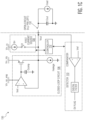
Figure 1C represents anexample fault state 130 detectable by the first example 100 open-circuit detector. The circuit in thisexample fault state 130 is the same as for example 100 except for an open-circuit (e.g. Pin Lift)event 132. -
Figure 1D represents a first example fault timing diagram 140 of the first open-circuit detector. When the pin-lift event 132 occurs (seeFigure 1C ), capacitor Cout is disconnected from the closed-loop circuit 106 output. Thus, when switch S1 is closed by thecontroller 112 then the current Ipu pulls the output voltage of the closed-loop circuit 106 higher than the overvoltage detection threshold after the pin-lift event 132 occurs. This overvoltage condition is detected by thedetector 110 which then sets the OV flag 116 (e.g. indicator) after a digital filter. In this example embodiment, Ipu is sufficiently large to overcome the leakage current Ileakage. Note that Cout voltage decays over time due to the external load or other leakage. -
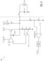
Figure 2 represents a second example 200 of the open-circuit detector. The second example 200 is substantially same as the first example 100 except for the addition of a current drain 202. The closed-loop circuit 106, firstcurrent source 108,detector 110, andcontroller 112 are still present in the second example 200 but are not labeled here to increase clarity. - The second example 200 of the open-circuit detector is applicable to example embodiments where the closed-loop circuit's 106 value of Tdis_chg (see
Figure 1B ) is larger than Toff (i.e. time during Tperiod not including Ton). In such example embodiments capacitor Cout is not be sufficiently discharged before the next current pulse is injected. This is occurs if Ileakage is relatively small. - To assist with the discharge, the current drain 202, having a drain current Ipd and a switch S2, is added to provided to more quickly discharge Cout. The switch S2 is also controlled by the
controller 112. -
Figure 3A represents a second example fault timing diagram 300 of the first example 100 open-circuit detector. Linear voltage regulators for loop stability are often compensated with an internal capacitor (Ccomp) connected to a gate of the regulators output driver (as shown inFigure 1A ). The value of the internal capacitor Ccomp is usually smaller than Cout by 5 to 6 orders of magnitude. - However, during an open-circuit (e.g. Pin Lift)
event 132, the compensation capacitor (Ccomp) in the closed-loop circuit 106 may need to be charged up by current source Ipu . If the current Ipu if is not large enough, the compensation capacitor (Ccomp) will take longer to charge and the closed-loop circuit 106 output voltage may not trigger an overvoltage flag within Ton as shown inFigure 3A . If Ipu is simply increased to charge the internal compensation capacitor (Ccomp) faster during a fault mode, design constraints on the acceptable ripple (seeFigure 1B ) during normal mode may be violated.Figure 3B shows an example solution to this concern. -
Figure 3B represents a third example 310 of the open-circuit detector. The third example 310 is substantially same as the first example 100 except for the addition of a second current source 312 (Icomp) and identification of anoutput driver 314. The closed-loop circuit 106, firstcurrent source 108,detector 110, andcontroller 112 are still present in the third example 310 but are not labeled here to increase clarity. The second current source 312 (Icomp) is activated by a third switch S3 by thecontroller 112 to overcome this issue, and is switched in parallel with the firstcurrent source 108, having the current (Ipu) and the switch (S1), to charge the compensation capacitor (Ccomp) faster for at least a part of the Ton time. -
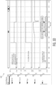
Figure 3C represents a first example timing diagram 320 of the third example 310 open-circuit detector. The first example timing diagram 320 shows various waveforms for the third example 310 open-circuit detector, including showing an OV (over voltage) duration with auxiliary current injection by the second current source 312 (Icomp). -
Figure 3D represents a second example timing diagram 330 of the third example 310 open-circuit detector. The second example timing diagram 330 shows various waveforms for the third example 310 open-circuit detector, including showing an OV (over voltage) duration without auxiliary current injection by the second current source 312 (Icomp). -
Figure 4 represents a fourth example 400 of the open-circuit detector. The fourth example 400 is an example implemented version of the first example 100 of the open-circuit detector. This example implemented version is configured to detect both an overvoltage and an undervoltage at Vout. Ileakage is modelled as resistors R1-2 and R3-5. -
Figure 5 represents a fifth example 500 of the open-circuit detector. The fifth example 500 of the open-circuit detector includes a closed-loop circuit 502, and an open-circuit detector. The open-circuit detector includes acurrent source 504, adetector 506, and acontroller 508. Thedetector 506 monitors a voltage at anoutput pin 510, and compares the voltage to a predetermined threshold voltage, which if exceeded during the Ipu current injection by thecurrent source 504, sets anOV flag 512. - An op-amp present in the closed-loop circuit 502 (e.g. linear voltage regulator) can be used as a comparator to detect a pin-lift event. When a pin-lift occurs, a gate of the linear regulator begins to turn an output FET of the closed-
loop circuit 502 off. The gate voltage is monitored to set the OV flag 512 (e.g. indicator). - Transistor M1 is a PMOS with its gate tied to the gate of the output FET of the closed-
loop circuit 502. The sources of M1 and the output FET are also shorted together. M1 is biased using a current source Ibias. M1 and current source Ibias essential form an internal comparator. - During a pin-lift event, the gate is pulled down, turning M1 ON and pulling its drain up. A level shifter in the
detector 506 is used to level shift this voltage to the digital supply before the flag is sent to thecontroller 508. - An advantage of the fifth example 500 of the open-circuit detector is a conventional two input comparator is not required. However, a speed of detection depends on the gm, bias currents and internal compensation capacitors within the closed-
loop circuit 106. - Various instructions and/or operational steps discussed in the above Figures can be executed in any order, unless a specific order is explicitly stated. Also, those skilled in the art will recognize that while some example sets of instructions/steps have been discussed, the material in this specification can be combined in a variety of ways to yield other examples as well, and are to be understood within a context provided by this detailed description.
- In some example embodiments these instructions/steps are implemented as functional and software instructions. In other embodiments, the instructions can be implemented either using logic gates, application specific chips, firmware, as well as other hardware forms.
- When the instructions are embodied as a set of executable instructions in a non-transitory computer-readable or computer-usable media which are effected on a computer or machine programmed with and controlled by said executable instructions. Said instructions are loaded for execution on a processor (such as one or more CPUs). Said processor includes microprocessors, microcontrollers, processor modules or subsystems (including one or more microprocessors or microcontrollers), or other control or computing devices. A processor can refer to a single component or to plural components. Said computer-readable or computer-usable storage medium or media is (are) considered to be part of an article (or article of manufacture). An article or article of manufacture can refer to any manufactured single component or multiple components. The non-transitory machine or computer-usable media or mediums as defined herein excludes signals, but such media or mediums may be capable of receiving and processing information from signals and/or other transitory mediums.
- It will be readily understood that the components of the embodiments as generally described herein and illustrated in the appended figures could be arranged and designed in a wide variety of different configurations. Thus, the detailed description of various embodiments, as represented in the figures, is not intended to limit the scope of the present disclosure, but is merely representative of various embodiments. While the various aspects of the embodiments are presented in drawings, the drawings are not necessarily drawn to scale unless specifically indicated.
- The present invention may be embodied in other specific forms without departing from its spirit or essential characteristics. The described embodiments are to be considered in all respects only as illustrative and not restrictive. The scope of the invention is, therefore, indicated by the appended claims rather than by this detailed description. All changes which come within the meaning and range of equivalency of the claims are to be embraced within their scope.
- Reference throughout this specification to features, advantages, or similar language does not imply that all of the features and advantages that may be realized with the present invention should be or are in any single embodiment of the invention. Rather, language referring to the features and advantages is understood to mean that a specific feature, advantage, or characteristic described in connection with an embodiment is included in at least one embodiment of the present invention. Thus, discussions of the features and advantages, and similar language, throughout this specification may, but do not necessarily, refer to the same embodiment.
- Furthermore, the described features, advantages, and characteristics of the invention may be combined in any suitable manner in one or more embodiments. One skilled in the relevant art will recognize, in light of the description herein, that the invention can be practiced without one or more of the specific features or advantages of a particular embodiment. In other instances, additional features and advantages may be recognized in certain embodiments that may not be present in all embodiments of the invention.
- Reference throughout this specification to "one embodiment," "an embodiment," or similar language means that a particular feature, structure, or characteristic described in connection with the indicated embodiment is included in at least one embodiment of the present invention. Thus, the phrases "in one embodiment," "in an embodiment," and similar language throughout this specification may, but do not necessarily, all refer to the same embodiment.
Claims (15)
- An open-circuit detector, comprising:a first current source configured to inject a current at an output of a closed-loop circuit;a detector configured to monitor a voltage of the closed-loop circuit;wherein the detector is configured to indicate whether the voltage monitored exceeds a predetermined threshold voltage;a controller configured to regulate the current injected by the first current source;wherein the controller is configured to set an open-circuit flag if the current injected caused the voltage to exceed the predetermined threshold voltage.
- The detector of claim 1:
wherein the controller is configured to set the open-circuit flag if the voltage exceeded the predetermined threshold voltage within a predetermined time after the current was injected. - The detector of claim 1 or 2:
wherein the voltage monitored by the detector is at a regulated output of the closed-loop circuit. - The detector of claim 1 or 2:
wherein the voltage monitored by the detector is at a node internal to the closed-loop circuit. - The detector of any preceding claim:
wherein the controller is configured to cause the first current source to inject the current while the closed-loop circuit is operating. - The detector of any preceding claim:
wherein the controller is configured to cause the first current source to inject the current at multiple intervals after the closed-loop circuit starts operating and before the closed-loop circuit stops operating. - The detector of any preceding claim:
wherein the controller is configured to adjust an amplitude or duration of the current injected by the first current source based on a load current drawn at the output of the closed-loop circuit. - The detector of any preceding claim:further comprising a current drain coupled between the output and a ground;wherein the controller is configured to adjust an amount of a current drained by the current drain based on a discharge time of an external load capacitor coupled to the output.
- The detector of any preceding claim:wherein the output of the closed-loop circuit is configured to be coupled an external capacitor configured to keep the output voltage within a predetermined ripple voltage range; andwherein the current injected by the current source does not cause the output voltage to exceed the predetermined ripple voltage range.
- The detector of any preceding claim:wherein the closed-loop circuit is a voltage regulator including an output driver and a compensation capacitor;wherein the compensation capacitor is coupled to a gate of the output driver;further comprising a second current source coupled in parallel with the first current source;wherein the controller is configured to adjust a duration or amplitude of the current injected by the second current source based on a value of the compensation capacitor.
- The detector of any preceding claim:
wherein the closed-loop circuit is a voltage regulator. - The detector of claim 11:
wherein the voltage regulator is a low drop out (LDO) regulator. - The detector of claim 11 or 12:
wherein the current is a pull up current injected at an output lead of the voltage regulator. - The detector of any preceding claim:
wherein the open-circuit detector is embedded within an integrated circuit. - The detector of any preceding claim:
wherein the detector is coupled to monitor the voltage at an output pin of a chip package.
Applications Claiming Priority (1)
| Application Number | Priority Date | Filing Date | Title |
|---|---|---|---|
| US17/804,844 US11874340B2 (en) | 2022-05-31 | 2022-05-31 | Open-circuit detector |
Publications (2)
| Publication Number | Publication Date |
|---|---|
| EP4286873A1 true EP4286873A1 (en) | 2023-12-06 |
| EP4286873B1 EP4286873B1 (en) | 2024-11-20 |
Family
ID=86331005
Family Applications (1)
| Application Number | Title | Priority Date | Filing Date |
|---|---|---|---|
| EP23172413.9A Active EP4286873B1 (en) | 2022-05-31 | 2023-05-09 | Open-circuit detector |
Country Status (3)
| Country | Link |
|---|---|
| US (1) | US11874340B2 (en) |
| EP (1) | EP4286873B1 (en) |
| CN (1) | CN117148217A (en) |
Families Citing this family (1)
| Publication number | Priority date | Publication date | Assignee | Title |
|---|---|---|---|---|
| US12549090B2 (en) | 2023-03-16 | 2026-02-10 | Nxp Usa, Inc. | Direct current DC-DC converter pin lift detection |
Citations (4)
| Publication number | Priority date | Publication date | Assignee | Title |
|---|---|---|---|---|
| US6295621B1 (en) * | 1993-04-22 | 2001-09-25 | Medtronic, Inc | Apparatus for detecting output bond integrity in a display driver circuit |
| US20190361068A1 (en) * | 2018-05-22 | 2019-11-28 | Texas Instruments Incorporated | Method and circuitry for open load detection |
| US20210190858A1 (en) * | 2019-12-18 | 2021-06-24 | Rohm Co., Ltd. | Semiconductor integrated circuit device |
| WO2021165447A1 (en) * | 2020-02-21 | 2021-08-26 | Signify Holding B.V. | Voltage sensing circuit and method |
Family Cites Families (8)
| Publication number | Priority date | Publication date | Assignee | Title |
|---|---|---|---|---|
| EP1465313B1 (en) | 2003-04-02 | 2010-04-28 | Semiconductor Components Industries, LLC | Method and device for short circuit or open load detection |
| WO2007082557A2 (en) | 2006-01-18 | 2007-07-26 | Freescale Semiconductor, Inc. | Regulated voltage system and method of protection therefor |
| DE102006045308B4 (en) | 2006-09-26 | 2011-07-21 | Continental Automotive GmbH, 30165 | Circuit arrangement for detecting the state of a load device which can be connected to a switching connection and method for operating such a circuit arrangement |
| US10338126B2 (en) * | 2016-04-15 | 2019-07-02 | Infineon Technologies Ag | Open load detection in output stages |
| DE102017201210A1 (en) | 2017-01-26 | 2018-07-26 | Robert Bosch Gmbh | Method and circuit arrangement for detecting a state of a load connected to a circuit connection |
| DE102017201705B4 (en) | 2017-02-02 | 2019-03-14 | Dialog Semiconductor (Uk) Limited | Voltage regulator with output capacitor measurement |
| EP3470954B1 (en) | 2017-10-10 | 2020-08-05 | NXP USA, Inc. | Closed-loop system oscillation detector |
| CN114114068B (en) * | 2020-08-28 | 2024-07-02 | 台达电子工业股份有限公司 | Motor connection fault detection method |
-
2022
- 2022-05-31 US US17/804,844 patent/US11874340B2/en active Active
-
2023
- 2023-05-09 EP EP23172413.9A patent/EP4286873B1/en active Active
- 2023-05-23 CN CN202310592152.4A patent/CN117148217A/en active Pending
Patent Citations (4)
| Publication number | Priority date | Publication date | Assignee | Title |
|---|---|---|---|---|
| US6295621B1 (en) * | 1993-04-22 | 2001-09-25 | Medtronic, Inc | Apparatus for detecting output bond integrity in a display driver circuit |
| US20190361068A1 (en) * | 2018-05-22 | 2019-11-28 | Texas Instruments Incorporated | Method and circuitry for open load detection |
| US20210190858A1 (en) * | 2019-12-18 | 2021-06-24 | Rohm Co., Ltd. | Semiconductor integrated circuit device |
| WO2021165447A1 (en) * | 2020-02-21 | 2021-08-26 | Signify Holding B.V. | Voltage sensing circuit and method |
Also Published As
| Publication number | Publication date |
|---|---|
| CN117148217A (en) | 2023-12-01 |
| US11874340B2 (en) | 2024-01-16 |
| EP4286873B1 (en) | 2024-11-20 |
| US20230384396A1 (en) | 2023-11-30 |
Similar Documents
| Publication | Publication Date | Title |
|---|---|---|
| US8384367B2 (en) | Step-down switching regulator | |
| US9608509B2 (en) | Switching converter with controllable restart delay and associated control method | |
| US11652400B2 (en) | Protection circuit with a cut-off switch for power systems | |
| US20140285935A1 (en) | Electronic fuse apparatus and method of operating the same | |
| CN113872436A (en) | Phase redundancy power supply with ORING field effect transistor current sensing | |
| KR20080046081A (en) | Protective circuit and its method | |
| US20170279363A1 (en) | Insulated synchronous rectification dc/dc converter | |
| US9627962B2 (en) | Fast blocking switch | |
| US7675267B2 (en) | Control circuit of power supply and control method of the power supply | |
| US12081125B2 (en) | Control circuit of DC/DC converter, power supply circuit, and electronic device | |
| JP2002084742A (en) | Overcurrent protection operation control method for step-down DCDC converter, overcurrent protection operation determination integrated circuit for step-down DCDC converter, overcurrent protection operation determination circuit module for step-down DCDC converter, control integrated circuit for step-down DCDC converter, and substrate for computer | |
| US10756626B2 (en) | Power conversion circuit | |
| KR20210147335A (en) | Inrush current limiter and system including the same | |
| EP4286873B1 (en) | Open-circuit detector | |
| US7576531B2 (en) | Switching regulator and electronic device therewith | |
| US7759920B2 (en) | Switching regulator and semiconductor device having the same | |
| US12267003B2 (en) | Power converter and control method for power converter | |
| JP7322302B2 (en) | Voltage detection circuit and method | |
| US11411500B2 (en) | Voltage feedback continuity failure detection in voltage regulators | |
| CN101958532A (en) | Device and method for over-current protection of DC-DC converter | |
| US11906999B2 (en) | Voltage overshoot dampener in dropout condition | |
| US20190131785A1 (en) | Reverse voltage recovery circuit | |
| CN117242415A (en) | Voltage Overshoot Suppressor under Voltage Loss Conditions | |
| US12149167B2 (en) | Methods, systems, and devices for fault handling in a power converter | |
| US12253871B2 (en) | Voltage overshoot dampener in dropout condition |
Legal Events
| Date | Code | Title | Description |
|---|---|---|---|
| PUAI | Public reference made under article 153(3) epc to a published international application that has entered the european phase |
Free format text: ORIGINAL CODE: 0009012 |
|
| STAA | Information on the status of an ep patent application or granted ep patent |
Free format text: STATUS: THE APPLICATION HAS BEEN PUBLISHED |
|
| AK | Designated contracting states |
Kind code of ref document: A1 Designated state(s): AL AT BE BG CH CY CZ DE DK EE ES FI FR GB GR HR HU IE IS IT LI LT LU LV MC ME MK MT NL NO PL PT RO RS SE SI SK SM TR |
|
| STAA | Information on the status of an ep patent application or granted ep patent |
Free format text: STATUS: REQUEST FOR EXAMINATION WAS MADE |
|
| 17P | Request for examination filed |
Effective date: 20240606 |
|
| RBV | Designated contracting states (corrected) |
Designated state(s): AL AT BE BG CH CY CZ DE DK EE ES FI FR GB GR HR HU IE IS IT LI LT LU LV MC ME MK MT NL NO PL PT RO RS SE SI SK SM TR |
|
| GRAP | Despatch of communication of intention to grant a patent |
Free format text: ORIGINAL CODE: EPIDOSNIGR1 |
|
| STAA | Information on the status of an ep patent application or granted ep patent |
Free format text: STATUS: GRANT OF PATENT IS INTENDED |
|
| INTG | Intention to grant announced |
Effective date: 20240830 |
|
| GRAS | Grant fee paid |
Free format text: ORIGINAL CODE: EPIDOSNIGR3 |
|
| GRAA | (expected) grant |
Free format text: ORIGINAL CODE: 0009210 |
|
| STAA | Information on the status of an ep patent application or granted ep patent |
Free format text: STATUS: THE PATENT HAS BEEN GRANTED |
|
| AK | Designated contracting states |
Kind code of ref document: B1 Designated state(s): AL AT BE BG CH CY CZ DE DK EE ES FI FR GB GR HR HU IE IS IT LI LT LU LV MC ME MK MT NL NO PL PT RO RS SE SI SK SM TR |
|
| REG | Reference to a national code |
Ref country code: GB Ref legal event code: FG4D |
|
| REG | Reference to a national code |
Ref country code: CH Ref legal event code: EP |
|
| REG | Reference to a national code |
Ref country code: DE Ref legal event code: R096 Ref document number: 602023001075 Country of ref document: DE |
|
| REG | Reference to a national code |
Ref country code: IE Ref legal event code: FG4D |
|
| REG | Reference to a national code |
Ref country code: LT Ref legal event code: MG9D |
|
| REG | Reference to a national code |
Ref country code: NL Ref legal event code: MP Effective date: 20241120 |
|
| PG25 | Lapsed in a contracting state [announced via postgrant information from national office to epo] |
Ref country code: IS Free format text: LAPSE BECAUSE OF FAILURE TO SUBMIT A TRANSLATION OF THE DESCRIPTION OR TO PAY THE FEE WITHIN THE PRESCRIBED TIME-LIMIT Effective date: 20250320 Ref country code: PT Free format text: LAPSE BECAUSE OF FAILURE TO SUBMIT A TRANSLATION OF THE DESCRIPTION OR TO PAY THE FEE WITHIN THE PRESCRIBED TIME-LIMIT Effective date: 20250320 Ref country code: HR Free format text: LAPSE BECAUSE OF FAILURE TO SUBMIT A TRANSLATION OF THE DESCRIPTION OR TO PAY THE FEE WITHIN THE PRESCRIBED TIME-LIMIT Effective date: 20241120 |
|
| PG25 | Lapsed in a contracting state [announced via postgrant information from national office to epo] |
Ref country code: FI Free format text: LAPSE BECAUSE OF FAILURE TO SUBMIT A TRANSLATION OF THE DESCRIPTION OR TO PAY THE FEE WITHIN THE PRESCRIBED TIME-LIMIT Effective date: 20241120 Ref country code: NL Free format text: LAPSE BECAUSE OF FAILURE TO SUBMIT A TRANSLATION OF THE DESCRIPTION OR TO PAY THE FEE WITHIN THE PRESCRIBED TIME-LIMIT Effective date: 20241120 |
|
| REG | Reference to a national code |
Ref country code: AT Ref legal event code: MK05 Ref document number: 1744041 Country of ref document: AT Kind code of ref document: T Effective date: 20241120 |
|
| PG25 | Lapsed in a contracting state [announced via postgrant information from national office to epo] |
Ref country code: BG Free format text: LAPSE BECAUSE OF FAILURE TO SUBMIT A TRANSLATION OF THE DESCRIPTION OR TO PAY THE FEE WITHIN THE PRESCRIBED TIME-LIMIT Effective date: 20241120 |
|
| PG25 | Lapsed in a contracting state [announced via postgrant information from national office to epo] |
Ref country code: ES Free format text: LAPSE BECAUSE OF FAILURE TO SUBMIT A TRANSLATION OF THE DESCRIPTION OR TO PAY THE FEE WITHIN THE PRESCRIBED TIME-LIMIT Effective date: 20241120 |
|
| PG25 | Lapsed in a contracting state [announced via postgrant information from national office to epo] |
Ref country code: NO Free format text: LAPSE BECAUSE OF FAILURE TO SUBMIT A TRANSLATION OF THE DESCRIPTION OR TO PAY THE FEE WITHIN THE PRESCRIBED TIME-LIMIT Effective date: 20250220 |
|
| PG25 | Lapsed in a contracting state [announced via postgrant information from national office to epo] |
Ref country code: LV Free format text: LAPSE BECAUSE OF FAILURE TO SUBMIT A TRANSLATION OF THE DESCRIPTION OR TO PAY THE FEE WITHIN THE PRESCRIBED TIME-LIMIT Effective date: 20241120 Ref country code: GR Free format text: LAPSE BECAUSE OF FAILURE TO SUBMIT A TRANSLATION OF THE DESCRIPTION OR TO PAY THE FEE WITHIN THE PRESCRIBED TIME-LIMIT Effective date: 20250221 Ref country code: AT Free format text: LAPSE BECAUSE OF FAILURE TO SUBMIT A TRANSLATION OF THE DESCRIPTION OR TO PAY THE FEE WITHIN THE PRESCRIBED TIME-LIMIT Effective date: 20241120 |
|
| PG25 | Lapsed in a contracting state [announced via postgrant information from national office to epo] |
Ref country code: PL Free format text: LAPSE BECAUSE OF FAILURE TO SUBMIT A TRANSLATION OF THE DESCRIPTION OR TO PAY THE FEE WITHIN THE PRESCRIBED TIME-LIMIT Effective date: 20241120 |
|
| PG25 | Lapsed in a contracting state [announced via postgrant information from national office to epo] |
Ref country code: RS Free format text: LAPSE BECAUSE OF FAILURE TO SUBMIT A TRANSLATION OF THE DESCRIPTION OR TO PAY THE FEE WITHIN THE PRESCRIBED TIME-LIMIT Effective date: 20250220 |
|
| PG25 | Lapsed in a contracting state [announced via postgrant information from national office to epo] |
Ref country code: SM Free format text: LAPSE BECAUSE OF FAILURE TO SUBMIT A TRANSLATION OF THE DESCRIPTION OR TO PAY THE FEE WITHIN THE PRESCRIBED TIME-LIMIT Effective date: 20241120 |
|
| PGFP | Annual fee paid to national office [announced via postgrant information from national office to epo] |
Ref country code: DE Payment date: 20250423 Year of fee payment: 3 |
|
| PG25 | Lapsed in a contracting state [announced via postgrant information from national office to epo] |
Ref country code: DK Free format text: LAPSE BECAUSE OF FAILURE TO SUBMIT A TRANSLATION OF THE DESCRIPTION OR TO PAY THE FEE WITHIN THE PRESCRIBED TIME-LIMIT Effective date: 20241120 |
|
| PG25 | Lapsed in a contracting state [announced via postgrant information from national office to epo] |
Ref country code: EE Free format text: LAPSE BECAUSE OF FAILURE TO SUBMIT A TRANSLATION OF THE DESCRIPTION OR TO PAY THE FEE WITHIN THE PRESCRIBED TIME-LIMIT Effective date: 20241120 |
|
| PG25 | Lapsed in a contracting state [announced via postgrant information from national office to epo] |
Ref country code: RO Free format text: LAPSE BECAUSE OF FAILURE TO SUBMIT A TRANSLATION OF THE DESCRIPTION OR TO PAY THE FEE WITHIN THE PRESCRIBED TIME-LIMIT Effective date: 20241120 |
|
| PG25 | Lapsed in a contracting state [announced via postgrant information from national office to epo] |
Ref country code: SK Free format text: LAPSE BECAUSE OF FAILURE TO SUBMIT A TRANSLATION OF THE DESCRIPTION OR TO PAY THE FEE WITHIN THE PRESCRIBED TIME-LIMIT Effective date: 20241120 |
|
| PG25 | Lapsed in a contracting state [announced via postgrant information from national office to epo] |
Ref country code: CZ Free format text: LAPSE BECAUSE OF FAILURE TO SUBMIT A TRANSLATION OF THE DESCRIPTION OR TO PAY THE FEE WITHIN THE PRESCRIBED TIME-LIMIT Effective date: 20241120 |
|
| PG25 | Lapsed in a contracting state [announced via postgrant information from national office to epo] |
Ref country code: IT Free format text: LAPSE BECAUSE OF FAILURE TO SUBMIT A TRANSLATION OF THE DESCRIPTION OR TO PAY THE FEE WITHIN THE PRESCRIBED TIME-LIMIT Effective date: 20241120 |
|
| P01 | Opt-out of the competence of the unified patent court (upc) registered |
Free format text: CASE NUMBER: APP_29981/2025 Effective date: 20250623 |
|
| REG | Reference to a national code |
Ref country code: DE Ref legal event code: R097 Ref document number: 602023001075 Country of ref document: DE |
|
| PG25 | Lapsed in a contracting state [announced via postgrant information from national office to epo] |
Ref country code: SE Free format text: LAPSE BECAUSE OF FAILURE TO SUBMIT A TRANSLATION OF THE DESCRIPTION OR TO PAY THE FEE WITHIN THE PRESCRIBED TIME-LIMIT Effective date: 20241120 |
|
| PLBE | No opposition filed within time limit |
Free format text: ORIGINAL CODE: 0009261 |
|
| STAA | Information on the status of an ep patent application or granted ep patent |
Free format text: STATUS: NO OPPOSITION FILED WITHIN TIME LIMIT |
|
| 26N | No opposition filed |
Effective date: 20250821 |
|
| PG25 | Lapsed in a contracting state [announced via postgrant information from national office to epo] |
Ref country code: LU Free format text: LAPSE BECAUSE OF NON-PAYMENT OF DUE FEES Effective date: 20250509 |
|
| REG | Reference to a national code |
Ref country code: BE Ref legal event code: MM Effective date: 20250531 |
|
| PG25 | Lapsed in a contracting state [announced via postgrant information from national office to epo] |
Ref country code: MC Free format text: LAPSE BECAUSE OF FAILURE TO SUBMIT A TRANSLATION OF THE DESCRIPTION OR TO PAY THE FEE WITHIN THE PRESCRIBED TIME-LIMIT Effective date: 20241120 |
|
| PG25 | Lapsed in a contracting state [announced via postgrant information from national office to epo] |
Ref country code: IE Free format text: LAPSE BECAUSE OF NON-PAYMENT OF DUE FEES Effective date: 20250509 |
|
| PG25 | Lapsed in a contracting state [announced via postgrant information from national office to epo] |
Ref country code: BE Free format text: LAPSE BECAUSE OF NON-PAYMENT OF DUE FEES Effective date: 20250531 |
|
| PG25 | Lapsed in a contracting state [announced via postgrant information from national office to epo] |
Ref country code: FR Free format text: LAPSE BECAUSE OF NON-PAYMENT OF DUE FEES Effective date: 20250531 |