EP4283822A1 - Electronic device - Google Patents
Electronic device Download PDFInfo
- Publication number
- EP4283822A1 EP4283822A1 EP22920088.6A EP22920088A EP4283822A1 EP 4283822 A1 EP4283822 A1 EP 4283822A1 EP 22920088 A EP22920088 A EP 22920088A EP 4283822 A1 EP4283822 A1 EP 4283822A1
- Authority
- EP
- European Patent Office
- Prior art keywords
- voltage
- pin
- detection circuit
- input terminal
- electronic device
- Prior art date
- Legal status (The legal status is an assumption and is not a legal conclusion. Google has not performed a legal analysis and makes no representation as to the accuracy of the status listed.)
- Pending
Links
Images



Classifications
-
- H—ELECTRICITY
- H02—GENERATION; CONVERSION OR DISTRIBUTION OF ELECTRIC POWER
- H02J—ELECTRIC POWER NETWORKS; CIRCUIT ARRANGEMENTS OR SYSTEMS FOR SUPPLYING OR DISTRIBUTING ELECTRIC POWER; SYSTEMS FOR STORING ELECTRIC ENERGY
- H02J7/00—Circuit arrangements for charging or discharging batteries or for supplying loads from batteries
- H02J7/40—Circuit arrangements for charging or discharging batteries or for supplying loads from batteries characterised by the exchange of charge or discharge related data
- H02J7/42—Circuit arrangements for charging or discharging batteries or for supplying loads from batteries characterised by the exchange of charge or discharge related data with electronic devices having internal batteries, e.g. mobile phones
-
- H—ELECTRICITY
- H02—GENERATION; CONVERSION OR DISTRIBUTION OF ELECTRIC POWER
- H02J—ELECTRIC POWER NETWORKS; CIRCUIT ARRANGEMENTS OR SYSTEMS FOR SUPPLYING OR DISTRIBUTING ELECTRIC POWER; SYSTEMS FOR STORING ELECTRIC ENERGY
- H02J7/00—Circuit arrangements for charging or discharging batteries or for supplying loads from batteries
- H02J7/60—Circuit arrangements for charging or discharging batteries or for supplying loads from batteries including safety or protection arrangements
- H02J7/64—Circuit arrangements for charging or discharging batteries or for supplying loads from batteries including safety or protection arrangements against overvoltage
-
- H—ELECTRICITY
- H02—GENERATION; CONVERSION OR DISTRIBUTION OF ELECTRIC POWER
- H02H—EMERGENCY PROTECTIVE CIRCUIT ARRANGEMENTS
- H02H9/00—Emergency protective circuit arrangements for limiting excess current or voltage without disconnection
- H02H9/04—Emergency protective circuit arrangements for limiting excess current or voltage without disconnection responsive to excess voltage
-
- H—ELECTRICITY
- H02—GENERATION; CONVERSION OR DISTRIBUTION OF ELECTRIC POWER
- H02J—ELECTRIC POWER NETWORKS; CIRCUIT ARRANGEMENTS OR SYSTEMS FOR SUPPLYING OR DISTRIBUTING ELECTRIC POWER; SYSTEMS FOR STORING ELECTRIC ENERGY
- H02J7/00—Circuit arrangements for charging or discharging batteries or for supplying loads from batteries
- H02J7/40—Circuit arrangements for charging or discharging batteries or for supplying loads from batteries characterised by the exchange of charge or discharge related data
-
- H—ELECTRICITY
- H02—GENERATION; CONVERSION OR DISTRIBUTION OF ELECTRIC POWER
- H02J—ELECTRIC POWER NETWORKS; CIRCUIT ARRANGEMENTS OR SYSTEMS FOR SUPPLYING OR DISTRIBUTING ELECTRIC POWER; SYSTEMS FOR STORING ELECTRIC ENERGY
- H02J7/00—Circuit arrangements for charging or discharging batteries or for supplying loads from batteries
- H02J7/40—Circuit arrangements for charging or discharging batteries or for supplying loads from batteries characterised by the exchange of charge or discharge related data
- H02J7/47—Arrangements for checking compatibility or authentication between one component, e.g. a battery or a battery charger, and another component, e.g. a power source
-
- H—ELECTRICITY
- H02—GENERATION; CONVERSION OR DISTRIBUTION OF ELECTRIC POWER
- H02J—ELECTRIC POWER NETWORKS; CIRCUIT ARRANGEMENTS OR SYSTEMS FOR SUPPLYING OR DISTRIBUTING ELECTRIC POWER; SYSTEMS FOR STORING ELECTRIC ENERGY
- H02J7/00—Circuit arrangements for charging or discharging batteries or for supplying loads from batteries
- H02J7/90—Regulation of charging or discharging current or voltage
- H02J7/933—Regulation of charging or discharging current or voltage the cycle being controlled or terminated in response to electric parameters
-
- H—ELECTRICITY
- H02—GENERATION; CONVERSION OR DISTRIBUTION OF ELECTRIC POWER
- H02H—EMERGENCY PROTECTIVE CIRCUIT ARRANGEMENTS
- H02H3/00—Emergency protective circuit arrangements for automatic disconnection directly responsive to an undesired change from normal electric working condition with or without subsequent reconnection ; integrated protection
- H02H3/08—Emergency protective circuit arrangements for automatic disconnection directly responsive to an undesired change from normal electric working condition with or without subsequent reconnection ; integrated protection responsive to excess current
- H02H3/087—Emergency protective circuit arrangements for automatic disconnection directly responsive to an undesired change from normal electric working condition with or without subsequent reconnection ; integrated protection responsive to excess current for DC applications
-
- H—ELECTRICITY
- H02—GENERATION; CONVERSION OR DISTRIBUTION OF ELECTRIC POWER
- H02J—ELECTRIC POWER NETWORKS; CIRCUIT ARRANGEMENTS OR SYSTEMS FOR SUPPLYING OR DISTRIBUTING ELECTRIC POWER; SYSTEMS FOR STORING ELECTRIC ENERGY
- H02J2207/00—Details of circuit arrangements for charging or discharging batteries or supplying loads from batteries
- H02J2207/30—Charge provided using DC bus or data bus of a computer
-
- Y—GENERAL TAGGING OF NEW TECHNOLOGICAL DEVELOPMENTS; GENERAL TAGGING OF CROSS-SECTIONAL TECHNOLOGIES SPANNING OVER SEVERAL SECTIONS OF THE IPC; TECHNICAL SUBJECTS COVERED BY FORMER USPC CROSS-REFERENCE ART COLLECTIONS [XRACs] AND DIGESTS
- Y02—TECHNOLOGIES OR APPLICATIONS FOR MITIGATION OR ADAPTATION AGAINST CLIMATE CHANGE
- Y02B—CLIMATE CHANGE MITIGATION TECHNOLOGIES RELATED TO BUILDINGS, e.g. HOUSING, HOUSE APPLIANCES OR RELATED END-USER APPLICATIONS
- Y02B40/00—Technologies aiming at improving the efficiency of home appliances, e.g. induction cooking or efficient technologies for refrigerators, freezers or dish washers
Definitions
- This application relates to the field of charging and discharging technologies, and in particular, to an electronic device.
- a voltage at which a battery of an electronic device is charged is getting higher and higher, so a voltage carried by a pin, which is configured to transmit a charging voltage, in a charging interface of the electronic device is getting higher and higher.
- a maximum voltage of a current VBUS pin configured to transmit the charging voltage may reach about 20 V.
- This application provides an electronic device, which can reduce breakdown of device components connected to a charging interface in the electronic device and reduce damage to components in the electronic device.
- an embodiment of this application provides an electronic device, the electronic device including an interface, a voltage detection circuit, and a processor, where
- the second voltage value is determined according to the voltage of the first pin when the power supply device transmits the charging voltage signal with the first voltage value to the second pin and the power supply devices supports fast charging, so as to prevent transmission of a charging voltage signal with an excessive voltage value to the second pin when the first pin and the second pin are short-circuited and then reduce breakdown of a following-stage component of the first pin caused by the excessive voltage value of the charging voltage signal, thereby reducing damage to components in the electronic device.
- the processor when determining the second voltage value according to the voltage of the first pin, is further configured to:
- the voltage detection circuit includes: a first ADC module and a first resistor, where
- that the input terminal of the voltage detection circuit is connected to an input terminal of the first ADC module through the first resistor includes: the input terminal of the voltage detection circuit being grounded through a second resistor and a third resistor connected in series, and a connection terminal of the second resistor and the third resistor being connected to the input terminal of the first ADC module through the first resistor.
- that the input terminal of the voltage detection circuit is connected to an input terminal of the first ADC module through the first resistor includes: the input terminal of the voltage detection circuit being connected to the input terminal of the first ADC module through a switch and the first resistor connected in series; and a control terminal of the switch being connected to the processor; and the processor is configured to: control the switch to be on when determining that the power supply device supports fast charging; and control the switch to be off after determining the second voltage value.
- the first ADC module is located in a power management unit (PMU) of the electronic device, or located in the processor.
- PMU power management unit
- the voltage detection circuit when detecting the voltage of the first pin, is further configured to: compare the voltage of the first pin with the preset first threshold, and send a comparison result to the processor.
- the voltage detection circuit includes:
- the interface is a Type-C interface
- the second pin is a VBUS pin
- the first pin is any data pin in the Type-C interface.
- an embodiment of this application provides a charging system, including a power supply device and the above electronic device.
- a current maximum voltage may reach about 20 V.
- FIG. 1A is a schematic structural diagram of pins of a Type-C interface.
- VBUS pins are pins configured to transmit a charging voltage
- pins such as SBU1, SBU2, CC1, CC2, TX1+, TX1-, TX2+, TX2-, RX1+, RX1-, RX2+, RX2-, D+, and D- are configured to transmit data signals.
- the above pins configured to transmit data signals are collectively referred to as data pins below.
- the above VBUS pins transmit a charging voltage generally no greater than 5 V.
- a maximum transmitted charging voltage may reach about 20 V.
- a maximum voltage value of the data signals transmitted by the above data pins is generally below 5 V, and some components of the electronic device that are connected to following stages thereof generally have a withstand voltage of about 6 V.
- the VBUS pins and the data pins in the Type-C interface transmit signals independently of each other. Therefore, when the data pins normally transmit data signals, components connected to following stages thereof (hereinafter referred to as following-stage components) generally may not be damaged due to breakdown.
- short circuiting may occur between the VBUS pins and other data pins in the Type-C interface.
- the VBUS pins and/or the data pins (for example, CC1 pins, TX1- pins, and the like) in the Type-C interface may tilt, causing short circuiting between the VBUS pins and adjacent data pins.
- an abnormal condition such as liquid or a foreign matter entering the Type-C interface causes short circuiting between one or more data pins and the VBUS pins in the Type-C interface.
- a maximum voltage of a charging voltage transmitted by a VBUS pin is about 20 V
- a withstand voltage of an analog switch (such as a headphone analog switch) connected to an SBU pin of the Type-C interface is only 6 V
- an analog switch such as a headphone analog switch
- a high voltage of 20 V on the VBUS pin can break down the analog switch, causing failure of the analog switch.
- the high voltage may also lead to failure of another following-stage component (such as Codec) connected to a following stage after the breakdown of the analog switch. As shown in FIG.
- a data pin D+/D- of the Type-C interface is connected to a common mode inductor in a following stage.
- the common mode inductor has channel impedance of about 3 ohms, a through-current capability of 100 mA, a peak value of 500 mA, and a mainboard following-stage TVS clamping voltage of 8.5 V
- the high voltage may cause the common mode inductor to be blown due to overcurrent, and may even cause the Type-C interface to be unusable.
- this application provides an electronic device, which can reduce breakdown of device components connected to a charging interface in the electronic device and reduce damage to components in the electronic device.
- FIG. 2 is a schematic diagram of a circuit structure of a charging system circuit in a charging scenario according to an embodiment of this application.
- the electronic device in this embodiment of this application will be illustrated below in conjunction with the circuit structure of the charging system in the charging scenario.
- the charging system may include: an electronic device 210, a power supply device 220, and a charging cable 230.
- the power supply device may be a charging head or another device capable of charging the electronic device.
- the electronic device 210 and the power supply device 220 are connected through the charging cable 230.
- the charging cable 230 is specifically connected to the electronic device through a Type-C interface. A manner in which the electronic device is charged by the power supply device through the charging cable may be called direct charging or cable charging.
- the electronic device 210 may include: a Type-C interface 211, a plug-in detection circuit 212, a protocol processing circuit 213, a processor 214, a power management unit (power management unit, PMU) 215, a battery pack 216, and a voltage detection circuit 217.
- the plug-in detection circuit 212 is respectively connected to a CC pin of the Type-C interface 211 and the processor 214.
- the plug-in detection circuit 212 is configured to detect, by detecting a voltage of the CC pin for example, whether a plug of the charging cable is plugged into the Type-C interface 211 of the electronic device, and send a first signal to the processor 214 when detecting that the plug of the charging cable is plugged into the Type-C interface 211 of the electronic device, to notify the processor 214 that the plug of the charging cable is plugged into the Type-C interface 211 of the electronic device.
- the plug-in detection circuit may be implemented by a related Type-C interface hot plug detection technology. A specific circuit implementation structure is not described in detail herein.
- the protocol processing circuit 213 is respectively connected to a CC/D+/D- pin of the Type-C interface 211 and the processor 214.
- the protocol processing circuit 213 is configured to communicate with the power supply device 220 through a charging protocol such as a USB Power Delivery (USB Power Delivery, USB-PD) protocol, and complete a communication negotiation process with the power supply device 220 based on the charging protocol.
- a charging protocol such as a USB Power Delivery (USB Power Delivery, USB-PD) protocol
- USB-PD USB Power Delivery
- the communication between the protocol processing circuit 213 and the power supply device 220 may be triggered by the processor 214.
- data communication may be performed between the protocol processing circuit 213 and the processor 214 through an I2C interface.
- the protocol processing circuit 213 may be implemented by using a related charging protocol processing chip. A specific circuit implementation structure is not described in detail herein.
- the PMU 215 is respectively connected to the VBUS pin of the Type-C interface 211, the processor 214, and the battery pack 216.
- the PMU 215 is configured to supply power to a power-consuming circuit in the electronic device 210 such as the processor 214 according to a charging voltage signal received from the VBUS pin, and the PMU 215 may be configured to charge the battery pack 216 of the electronic device according to the charging voltage signal.
- the PMU 215 may be implemented by using a related PMU chip. A specific circuit implementation structure is not described in detail herein.
- the voltage detection circuit 217 is respectively connected to a target pin (the SBU1 pin is taken as an example in FIG. 2 ) of the Type-C interface 211 and the processor 214.
- the voltage detection circuit 217 is configured to detect a voltage of the target pin and send a detection result to the processor 214.
- a specific implementation structure of the voltage detection circuit 217 is described more specifically hereinafter with reference to FIG. 4 to FIG. 8 . Details are not described herein.
- the charging voltage signal is specifically transmitted to the PMU 215 of the electronic device 210.
- the PMU 215 may supply power to the power-consuming circuit in the electronic device 210 such as the processor 214 according to the charging voltage signal, and the PMU 215 may charge the battery pack 216 of the electronic device according to the charging voltage signal.
- the protocol processing circuit 213 obtains charging-related information such as a power supply capability of the power supply device 220, and the protocol processing circuit 213 sends the charging-related information to the processor 214.
- the power supply capability may include: whether to support fast charging.
- Step S5 The voltage detection circuit 217 detects the voltage of the target pin (for example, the target pin is the SBU1 pin in FIG. 2 ) in the Type-C interface 211, and sends the detected voltage to the processor 214.
- the target pin for example, the target pin is the SBU1 pin in FIG. 2
- the processor 214 sends the detected voltage to the processor 214.
- the voltage detection circuit 217 may be enabled and controlled by the processor 214. Specifically, the processor 214 may send a first enable signal to the voltage detection circuit 217 after determining, according to the power supply capability of the power supply device 220, that the power supply device 220 supports fast charging, so as to control the voltage detection circuit 217 to start to detect the voltage of the target pin in the Type-C interface 211.
- Step S6 The processor 214 determines a charging voltage expected value for this charging according to the power supply capability of the power supply device 220 and the voltage of the target pin detected by the voltage detection circuit 217, and sends the determined charging voltage expected value to the protocol processing circuit 213, which is then sent to the power supply device 220 by the protocol processing circuit 213 via the data pin of the Type-C interface 211 and the charging cable 230.
- the charging voltage expected value may be the charging voltage value in the normal charging mode supported by the power supply device 220 (that is, a charging voltage value during non-fast charging), such as 5 V, or the charging voltage value of fast charging supported by the power supply device 220, such as 20 V
- the processor 214 after determining the charging voltage expected value for this charging, may send a second enable signal to the voltage detection circuit 217, so as to control the voltage detection circuit 217 to stop detecting the voltage of the target pin in the Type-C interface 211.
- Step S7 The power supply device 220 adjusts, according to the charging voltage expected value indicated by the electronic device 210, a voltage value of the charging voltage signal transmitted to the VBUS pin of the electronic device 210.
- the charging voltage signal of the power supply device 220 is still transmitted to the PMU 215 of the electronic device 210 via the charging cable 230 and the VBUS pin of the Type-C interface 211.
- the PMU 215 may supply power to the power-consuming circuit in the electronic device 210 such as the processor 214 according to the charging voltage signal, and the PMU 215 may charge the battery pack 216 of the electronic device according to the charging voltage signal.
- Step 301 The processor 214 determines, according to the power supply capability of the power supply device 220, whether the power supply device 220 supports fast charging. Step 302 is performed if fast charging is supported. Step 304 is performed if fast charging is not supported. In this step, a situation where the power supply device 220 supports fast charging can be screened out by determining whether the power supply device 220 supports fast charging, so as to further screen out short circuiting between the VBUS pin and the target pin in subsequent step 302.
- Step 302 Acquire the voltage of the target pin, determine whether the voltage of the target pin is greater than a preset first threshold, and if yes, perform step 304; and if not, perform step 303.
- the first threshold may be greater than a maximum voltage value (for example, 3.3 V) of a data signal transmitted by the target pin, and less than or equal to an initial voltage value (for example, 5 V) of the charging voltage signal when the power supply device 220 charges the electronic device 210.
- a maximum voltage value for example, 3.3 V
- an initial voltage value for example, 5 V
- step S4 whether short circuiting occurs between the target pin and the VBUS pin is determined by determining whether the voltage of the target pin is greater than the preset first threshold. This is because: if short circuiting occurs between the target pin and the VBUS pin, the voltage of the target pin should be equal to the voltage value of the charging voltage signal in step S4. When the voltage value is greater than the maximum voltage value of the data signal transmitted by the target pin, in other words, if the voltage of the target pin is greater than the maximum voltage value of the data signal transmitted by the target pin, it indicates that short circuiting occurs between the target pin and the VBUS pin.
- Step 303 Determine a charging voltage expected value to be a second value, where the second value may be the voltage value of the charging voltage signal in the fast charging mode.
- This step is performed after it is determined in step 301 that the power supply device 220 supports fast charging and it is determined in step 302 that the voltage of the target pin is no greater than the preset first threshold, that is, performed in the situation where the power supply device 220 supports fast charging and the target pin and the VBUS pin are not short-circuited.
- Charging efficiency of the electronic device can be improved by determining the charging voltage expected value to be the second value, for example, the voltage value in the fast charging mode.
- Step 304 Determine the charging voltage expected value to be a first value, where the first value may be the voltage value of the charging voltage signal in the normal charging mode.
- This step may be performed after it is determined in step 301 that the power supply device 220 does not support fast charging. Since the power supply device 220 does not support fast charging, the charging voltage expected value can only be determined to be the first value, that is, the voltage value in the normal charging mode. Alternatively, this step may be performed after it is determined in step 301 that the power supply device 220 supports fast charging and it is determined in step 302 that the voltage of the target pin is greater than the preset first threshold, that is, performed in the situation where the power supply device 220 supports fast charging but the target pin and the VBUS pin are short-circuited.
- the voltage value of the charging voltage signal can be ensured to be no greater than a withstand voltage of a following-stage component of the target pin by determining the charging voltage expected value to be the first value, for example, the voltage value in the normal charging mode, thereby ensuring that the charging voltage signal may not cause damage to the following-stage component of the target pin.
- FIG. 4 to FIG. 8 show only circuit structures such as the Type-C interface 211 and the processor 214 associated with the voltage detection circuit 217, omit circuit structures such as the plug-in detection circuit 212 and the protocol processing circuit 213 shown in FIG. 3 , and are not intended to limit specific implementation of the electronic device in the embodiments of this application.
- FIG. 4 is a schematic diagram of an implementation structure of a voltage detection circuit according to an embodiment of this application.
- FIG. 4 is based on an example in which the target pin is the SBU1 pin and a following-stage component connected to the SBU1 pin is the headphone analog switch. It should be noted that in practical applications, specific following-stage components in the electronic device that are connected to the SBU1 pin are not limited in this embodiment of this application.
- the voltage detection circuit 217 of the SBU1 pin may include: the SBU1 pin of the Type-C interface 211 being connected to a first signal input terminal IN01 of an analog-to-digital converter (ADC) module through a first resistor R1, and a first output terminal OUT01 of the ADC module being connected to a first input terminal IN11 of the processor.
- ADC analog-to-digital converter
- the ADC module is configured to convert an analog voltage signal received by the first signal input terminal IN01 into a digital voltage signal and output the digital voltage signal to the processor 214 through the first output terminal OUT01.
- the SBU1 pin is connected to the signal input terminal IN01 of the ADC module through the first resistor R1, so that the signal input terminal IN01 of the ADC module can detect a voltage signal of the SBU1 pin.
- the voltage signal is an analog voltage signal.
- the ADC module converts the detected analog voltage signal of the SBU1 pin into a digital voltage signal and then may transmit the digital voltage signal to the processor 214.
- FIG. 5 is a schematic diagram of a second implementation structure of the voltage detection circuit according to an embodiment of this application.
- FIG. 5 is still based on the example in which the target pin is the SBU1 pin and the following-stage component connected to the SBU1 pin is the headphone analog switch.
- the voltage detection circuit shown in FIG. 5 is mainly different from the voltage detection circuit shown in FIG. 4 in that: the SBU1 pin of the Type-C interface 211 is grounded through a second resistor R2 and a third resistor R3 connected in series, and a connection terminal A of the second resistor R2 and the third resistor R3 is connected to the first signal input terminal IN01 of the ADC module through the first resistor R1.
- the second resistor R2 and the third resistor R3 divide a voltage of the SBU1 pin, so that a voltage detected by the first signal input terminal IN01 of the ADC module is a voltage division signal of the SBU1 pin; and the ADC module converts the detected voltage division signal of the SBU1 pin into a digital voltage signal and then may transmit the digital voltage signal to the processor 214.
- the processor 214 may calculate a digital voltage signal of the SBU1 pin based on a digital voltage signal.
- a detection range of the ADC module may be less than the above first threshold.
- the analog voltage signal inputted to the ADC module may be in line with the detection range of the ADC module by adjusting voltage values of the second resistor R2 and the third resistor R3, thereby improving detection accuracy of the ADC module.
- Many devices of the electronic device are provided with ADC modules. For example, a processor chip, a PMU chip, and the like in the electronic device are provided with ADC modules. Therefore, to reduce occupation of a PCB area by the voltage detection circuit, an existing ADC module in the electronic device may be reused as the ADC module in the voltage detection circuit shown in FIG. 4 and FIG. 5 above.
- the existing ADC module in the above electronic device may be an ADC module disposed separately, or an ADC module included in an existing device (such as the PMU or the processor).
- the above existing device may be a device in a circuit branch connected to the target pin, or a device other than the circuit branch connected to the target pin.
- FIG. 6A is a schematic diagram of a third implementation structure of the voltage detection circuit according to an embodiment of this application.
- the ADC module in the voltage detection circuit shown in FIG. 4 is an existing ADC module in the PMU 215.
- FIG. 6B is a schematic diagram of a fourth implementation structure of the voltage detection circuit according to an embodiment of this application.
- the ADC module in the voltage detection circuit shown in FIG. 5 is an existing ADC module in the PMU 215.
- the voltage detection circuit may reuse the first signal input terminal IN01 of the ADC module with another existing device.
- a switch may be disposed in a branch where the first resistor R1 and the ADC module are located, and the processor only gates the switch when needing to detect the voltage of the target pin.
- FIG. 6C is taken as an example for illustration below.
- FIG. 6C is a schematic diagram of a fifth implementation structure of the voltage detection circuit according to an embodiment of this application.
- the above switch is added to the voltage detection circuit shown in FIG. 6A .
- a first switch K1 is added between the SBU1 pin and the first resistor R1, a control terminal of the first switch K1 may be connected to the processor 214, and the processor 214 controls the first switch K1 to be on when needing to obtain the voltage of the SBU1 pin and controls the first switch K1 to be off at other times.
- the target pin is the SBU1 pin.
- the target pin may alternatively be any other pin for data transmission in the Type-C interface, such as CC1, CC2, SBU2, D+, or D-. Illustration is provided below with reference to FIG. 7 .
- FIG. 7 is a schematic diagram of a sixth implementation structure of the voltage detection circuit according to an embodiment of this application, based on an example in which the target pin in the circuit shown in FIG. 5 is replaced with another pin.
- a difference from the circuit shown in FIG. 5 only lies in that: the target pin is replaced from the SBU1 pin to the CC1 or D+ or D- pin.
- the following-stage component of the target pin is the protocol processing circuit 213 (such as a PD/SOC/protocol IC).
- the above ADC module may be replaced with a comparator, a logic gate, or the like, or the voltage detection circuit may also reuse an IO pin of the SOC and detect the voltage of the target pin by detecting high and low levels through the IO pin. In the above manner, a smaller area of the PCB is also occupied. Illustration is provided below with reference to FIG. 8 .
- FIG. 8 is a schematic diagram of a seventh implementation structure of the voltage detection circuit according to an embodiment of this application, based on an example in which the ADC module in the voltage detection circuit shown in FIG. 4 is replaced with a comparator.
- the voltage detection circuit may include: a comparator A1 having a positive input terminal connected to the SBU1 pin of the Type-C interface through the first resistor R1, a negative input terminal receiving a reference voltage signal, and an output terminal connected to the processor 214.
- the comparator A1 is configured to: output a high-level signal through the output terminal when a voltage at the positive input terminal is higher than a voltage at the negative input terminal, and output a low-level signal through the output terminal when the voltage at the positive input terminal is no higher than the voltage at the negative input terminal.
- the positive input terminal of the comparator A1 may detect the voltage of the SBU1 pin, and a voltage value of the reference voltage signal at the negative input terminal may be a first threshold, so that the comparator A1 can compare the voltage of the SBU1 pin with a voltage of the reference voltage signal, and send a comparison result to the processor 214 through the outputted high-level signal or low-level signal.
- the processor can know, according to the received high-level signal or low-level signal, whether the voltage of the SBU1 pin is higher than the preset first threshold.
- the voltage detection circuit may be further configured to: compare the voltage of the first pin with the preset first threshold, and send a comparison result to the processor.
- the processor may determine the above expected voltage value according to the comparison result.
- the charging interface of the electronic device is a Type-C interface.
- the charging interface of the electronic device in the embodiments of this application may alternatively be another charging interface including a charging voltage signal transmission pin and a data pin other than the Type-C interface, such as another USB interface or a Lightning interface other than the Type-C interface, which is not limited in the embodiments of this application.
Landscapes
- Engineering & Computer Science (AREA)
- Power Engineering (AREA)
- Power Sources (AREA)
- Charge And Discharge Circuits For Batteries Or The Like (AREA)
Abstract
Description
- This application relates to the field of charging and discharging technologies, and in particular, to an electronic device.
- With the development of a fast charging technology, a voltage at which a battery of an electronic device is charged is getting higher and higher, so a voltage carried by a pin, which is configured to transmit a charging voltage, in a charging interface of the electronic device is getting higher and higher. In an example, if the charging interface is Type-C, a maximum voltage of a current VBUS pin configured to transmit the charging voltage may reach about 20 V.
- However, as the voltage carried by the pin increases, breakdown of device components connected to the charging interface in the electronic device also increases accordingly, resulting in damage to components in the electronic device.
- This application provides an electronic device, which can reduce breakdown of device components connected to a charging interface in the electronic device and reduce damage to components in the electronic device.
- According to a first aspect, an embodiment of this application provides an electronic device, the electronic device including an interface, a voltage detection circuit, and a processor, where
- the interface is configured to connect a power supply device, the interface includes a first pin and a second pin, the first pin being configured to transmit a data signal, and the second pin being configured to transmit a charging voltage signal; and the voltage detection circuit is respectively connected to the first pin and the processor;
- the voltage detection circuit is configured to: detect a voltage of the first pin; and
- the processor is configured to: determine a second voltage value according to the voltage of the first pin when the power supply device transmits a charging voltage signal with a first voltage value to the second pin and the power supply devices supports fast charging; and send the second voltage value to the power supply device for the power supply device to adjust a voltage value of the charging voltage signal to the second voltage value.
- In the electronic device, the second voltage value is determined according to the voltage of the first pin when the power supply device transmits the charging voltage signal with the first voltage value to the second pin and the power supply devices supports fast charging, so as to prevent transmission of a charging voltage signal with an excessive voltage value to the second pin when the first pin and the second pin are short-circuited and then reduce breakdown of a following-stage component of the first pin caused by the excessive voltage value of the charging voltage signal, thereby reducing damage to components in the electronic device.
- In a possible implementation, when determining the second voltage value according to the voltage of the first pin, the processor is further configured to:
- determine the second voltage value to be a first value when the voltage of the first pin is no less than a preset first threshold; and
- determine the second voltage value to be a second value when the voltage of the first pin is less than the preset first threshold; the first value being less than the second value, the first threshold being less than or equal to the first voltage value and greater than a maximum voltage value of the data signal transmitted by the first pin.
- In a possible implementation, the electronic device further includes a protocol processing circuit, the protocol processing circuit being respectively connected to a third pin of the interface and the processor, the third pin being configured to transmit a data signal; and
- when sending the second voltage value to the power supply device, the processor is further configured to:
send the second voltage value to the protocol processing circuit, the protocol processing circuit being configured to: send the second voltage value to the power supply device through the third pin of the interface. - In a possible implementation, the voltage detection circuit includes: a first ADC module and a first resistor, where
- an input terminal of the voltage detection circuit is configured to connect the first pin, and an output terminal is configured to connect the processor;
- the input terminal of the voltage detection circuit is connected to an input terminal of the first ADC module through the first resistor; an output terminal of the first ADC module is taken as the output terminal of the voltage detection circuit; and
- the first ADC module is configured to: convert a received analog voltage signal into a digital voltage signal, and send the digital voltage signal to the processor.
- In a possible implementation, that the input terminal of the voltage detection circuit is connected to an input terminal of the first ADC module through the first resistor includes:
the input terminal of the voltage detection circuit being grounded through a second resistor and a third resistor connected in series, and a connection terminal of the second resistor and the third resistor being connected to the input terminal of the first ADC module through the first resistor. - In a possible implementation, that the input terminal of the voltage detection circuit is connected to an input terminal of the first ADC module through the first resistor includes: the input terminal of the voltage detection circuit being connected to the input terminal of the first ADC module through a switch and the first resistor connected in series; and a control terminal of the switch being connected to the processor; and
the processor is configured to: control the switch to be on when determining that the power supply device supports fast charging; and control the switch to be off after determining the second voltage value. - In a possible implementation, the first ADC module is located in a power management unit (PMU) of the electronic device, or located in the processor.
- In a possible implementation, when detecting the voltage of the first pin, the voltage detection circuit is further configured to:
compare the voltage of the first pin with the preset first threshold, and send a comparison result to the processor. - In a possible implementation, the voltage detection circuit includes:
- an input terminal of the voltage detection circuit configured to connect the first pin, and an output terminal configured to connect the processor;
- where the input terminal of the voltage detection circuit is connected to a first input terminal of a comparator through a fourth resistor, a second input terminal of the comparator is connected to a reference voltage terminal, a voltage at the reference voltage terminal is the first threshold, and an output terminal of the comparator is taken as the output terminal of the voltage detection circuit; and
- the comparator is configured to: compare voltages received by the first input terminal and the second input terminal, and output a comparison result.
- In a possible implementation, the interface is a Type-C interface, the second pin is a VBUS pin, and the first pin is any data pin in the Type-C interface.
- According to a second aspect, an embodiment of this application provides a charging system, including a power supply device and the above electronic device.
- To describe the technical solutions in the embodiments of the present invention more clearly, the following briefly describes the accompanying drawings required for describing the embodiments. Apparently, the accompanying drawings in the following description show merely some embodiments of the present invention, and a person of ordinary skill in the art may still derive other drawings from these accompanying drawings without creative efforts.
-
FIG. 1A is a schematic structural diagram of pins of a Type-C interface; -
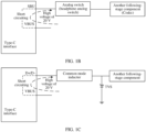
FIG. 1B is an example diagram of a circuit structure when a VBUS pin and an SBU pin are short-circuited; -
FIG. 1C is an example diagram of a circuit structure when a VBUS pin and a D+/D- pin are short-circuited; -
FIG. 2 is a schematic diagram of a circuit structure of a charging system in a charging scenario applicable to an electronic device according to this application; -
FIG. 3 is a schematic processing flowchart of an embodiment of a processor in an electronic device according to this application; -
FIG. 4 is a schematic structural diagram of an embodiment of a voltage detection circuit in an electronic device according to this application; -
FIG. 5 is a schematic structural diagram of another embodiment of the voltage detection circuit in the electronic device according to this application; -
FIG. 6A is a schematic structural diagram of a third embodiment of the voltage detection circuit in the electronic device according to this application; -
FIG. 6B is a schematic structural diagram of a fourth embodiment of the voltage detection circuit in the electronic device according to this application; -
FIG. 6C is a schematic structural diagram of a fifth embodiment of the voltage detection circuit in the electronic device according to this application; -
FIG. 7 is a schematic structural diagram of a sixth embodiment of the voltage detection circuit in the electronic device according to this application; and -
FIG. 8 is a schematic structural diagram of a seventh embodiment of the voltage detection circuit in the electronic device according to this application. - Terms used in implementations of this application are merely intended to explain specific embodiments of this application rather than limit this application.
- With the development of a fast charging technology, a voltage at which a battery of an electronic device is charged is getting higher and higher, so a voltage carried by a pin, which is configured to transmit a charging voltage, in a charging interface of the electronic device is getting higher and higher. A current maximum voltage may reach about 20 V.
- For example, the charging interface is Type-C.
FIG. 1A is a schematic structural diagram of pins of a Type-C interface. VBUS pins are pins configured to transmit a charging voltage, and pins such as SBU1, SBU2, CC1, CC2, TX1+, TX1-, TX2+, TX2-, RX1+, RX1-, RX2+, RX2-, D+, and D- are configured to transmit data signals. For the convenience of description, the above pins configured to transmit data signals are collectively referred to as data pins below. - In a normal charging mode (without fast charging), the above VBUS pins transmit a charging voltage generally no greater than 5 V. In a fast charging mode, a maximum transmitted charging voltage may reach about 20 V.
- A maximum voltage value of the data signals transmitted by the above data pins is generally below 5 V, and some components of the electronic device that are connected to following stages thereof generally have a withstand voltage of about 6 V.
- Under a normal circumstance, the VBUS pins and the data pins in the Type-C interface transmit signals independently of each other. Therefore, when the data pins normally transmit data signals, components connected to following stages thereof (hereinafter referred to as following-stage components) generally may not be damaged due to breakdown.
- However, in some scenarios, short circuiting may occur between the VBUS pins and other data pins in the Type-C interface. For example, the VBUS pins and/or the data pins (for example, CC1 pins, TX1- pins, and the like) in the Type-C interface may tilt, causing short circuiting between the VBUS pins and adjacent data pins. Alternatively, an abnormal condition such as liquid or a foreign matter entering the Type-C interface causes short circuiting between one or more data pins and the VBUS pins in the Type-C interface.
- In this case, if withstand voltages of following-stage components connected to the data pins short-circuited to the VBUS pins are lower than the charging voltage transmitted by the VBUS pins, the following-stage components may be broken down, resulting in damage to the following-stage components. For example, referring to
FIG. 1B , a maximum voltage of a charging voltage transmitted by a VBUS pin is about 20 V, and a withstand voltage of an analog switch (such as a headphone analog switch) connected to an SBU pin of the Type-C interface is only 6 V When the VBUS pin and the SBU pin are short-circuited due to a problem such as liquid ingress or a foreign matter on the Type-C interface, a high voltage of 20 V on the VBUS pin can break down the analog switch, causing failure of the analog switch. In addition, the high voltage may also lead to failure of another following-stage component (such as Codec) connected to a following stage after the breakdown of the analog switch. As shown inFIG. 1C , a data pin D+/D- of the Type-C interface is connected to a common mode inductor in a following stage. The common mode inductor has channel impedance of about 3 ohms, a through-current capability of 100 mA, a peak value of 500 mA, and a mainboard following-stage TVS clamping voltage of 8.5 V When the VBUS pin and the data pin D+/D- are short-circuited and the voltage transmitted by the VBUS pin reaches a high voltage of 20 V, the high voltage may cause the common mode inductor to be blown due to overcurrent, and may even cause the Type-C interface to be unusable. - To this end, this application provides an electronic device, which can reduce breakdown of device components connected to a charging interface in the electronic device and reduce damage to components in the electronic device.
-
FIG. 2 is a schematic diagram of a circuit structure of a charging system circuit in a charging scenario according to an embodiment of this application. The electronic device in this embodiment of this application will be illustrated below in conjunction with the circuit structure of the charging system in the charging scenario. - As shown in
FIG. 2 , the charging system may include: anelectronic device 210, apower supply device 220, and a chargingcable 230. The power supply device may be a charging head or another device capable of charging the electronic device. Theelectronic device 210 and thepower supply device 220 are connected through the chargingcable 230. The chargingcable 230 is specifically connected to the electronic device through a Type-C interface. A manner in which the electronic device is charged by the power supply device through the charging cable may be called direct charging or cable charging. - The
electronic device 210 may include: a Type-C interface 211, a plug-indetection circuit 212, aprotocol processing circuit 213, aprocessor 214, a power management unit (power management unit, PMU) 215, abattery pack 216, and avoltage detection circuit 217. - The plug-in
detection circuit 212 is respectively connected to a CC pin of the Type-C interface 211 and theprocessor 214. The plug-indetection circuit 212 is configured to detect, by detecting a voltage of the CC pin for example, whether a plug of the charging cable is plugged into the Type-C interface 211 of the electronic device, and send a first signal to theprocessor 214 when detecting that the plug of the charging cable is plugged into the Type-C interface 211 of the electronic device, to notify theprocessor 214 that the plug of the charging cable is plugged into the Type-C interface 211 of the electronic device. The plug-in detection circuit may be implemented by a related Type-C interface hot plug detection technology. A specific circuit implementation structure is not described in detail herein. - The
protocol processing circuit 213 is respectively connected to a CC/D+/D- pin of the Type-C interface 211 and theprocessor 214. Theprotocol processing circuit 213 is configured to communicate with thepower supply device 220 through a charging protocol such as a USB Power Delivery (USB Power Delivery, USB-PD) protocol, and complete a communication negotiation process with thepower supply device 220 based on the charging protocol. The communication between theprotocol processing circuit 213 and thepower supply device 220 may be triggered by theprocessor 214. Optionally, data communication may be performed between theprotocol processing circuit 213 and theprocessor 214 through an I2C interface. Theprotocol processing circuit 213 may be implemented by using a related charging protocol processing chip. A specific circuit implementation structure is not described in detail herein. ThePMU 215 is respectively connected to the VBUS pin of the Type-C interface 211, theprocessor 214, and thebattery pack 216. ThePMU 215 is configured to supply power to a power-consuming circuit in theelectronic device 210 such as theprocessor 214 according to a charging voltage signal received from the VBUS pin, and thePMU 215 may be configured to charge thebattery pack 216 of the electronic device according to the charging voltage signal. ThePMU 215 may be implemented by using a related PMU chip. A specific circuit implementation structure is not described in detail herein. - The
voltage detection circuit 217 is respectively connected to a target pin (the SBU1 pin is taken as an example inFIG. 2 ) of the Type-C interface 211 and theprocessor 214. Thevoltage detection circuit 217 is configured to detect a voltage of the target pin and send a detection result to theprocessor 214. A specific implementation structure of thevoltage detection circuit 217 is described more specifically hereinafter with reference toFIG. 4 to FIG. 8 . Details are not described herein. - An operating principle of the circuit shown in
FIG. 2 is illustrated: - Step S1: The plug-in
detection circuit 212 detects whether a plug of the charging cable is plugged into the Type-C interface 211 of the electronic device. The plug-indetection circuit 212 sends a first signal to theprocessor 214 if the plug-indetection circuit 212 detects that the plug of the charging cable is plugged into the Type-C interface 211 of theelectronic device 210. The first signal is used for indicating theprocessor 214 that the plug of the charging cable is plugged into the Type-C interface of the electronic device. - Step S2: The
processor 214 sends a second signal to theprotocol processing circuit 213 in response to the first signal. The second signal is used for instructing theprotocol processing circuit 213 to communicate with thepower supply device 220. - Step S3: The
protocol processing circuit 213 communicates, in response to the second signal, with thepower supply device 220 through a charging protocol such as a USB Power Delivery (USB Power Delivery, USB-PD) protocol, and completes a communication negotiation process with thepower supply device 220 based on the charging protocol. As shown inFIG. 2 , communication data between theprotocol processing circuit 213 and thepower supply device 220 may be transmitted through data transmission lines corresponding to a data pin (such as a CC1 pin, a CC2 pin, a D+ pin, or a D-pin) of the Type-C interface 211 and a data pin in the chargingcable 230. - Step S4: After the communication between the
protocol processing circuit 213 and thepower supply device 220 is completed, thepower supply device 220 starts to output, through the charging cable, a charging voltage signal to theelectronic device 210 via the chargingcable 230 and the VBUS pin of the Type-C interface 211. A voltage value of the charging voltage signal is generally the charging voltage value in the normal charging mode supported by thepower supply device 220, which may be, for example, 5 V. - The charging voltage signal is specifically transmitted to the
PMU 215 of theelectronic device 210. ThePMU 215 may supply power to the power-consuming circuit in theelectronic device 210 such as theprocessor 214 according to the charging voltage signal, and thePMU 215 may charge thebattery pack 216 of the electronic device according to the charging voltage signal. Moreover, after the communication between theprotocol processing circuit 213 and thepower supply device 220 is completed, theprotocol processing circuit 213 obtains charging-related information such as a power supply capability of thepower supply device 220, and theprotocol processing circuit 213 sends the charging-related information to theprocessor 214. The power supply capability may include: whether to support fast charging. - Step S5: The
voltage detection circuit 217 detects the voltage of the target pin (for example, the target pin is the SBU1 pin inFIG. 2 ) in the Type-C interface 211, and sends the detected voltage to theprocessor 214. - Optionally, the
voltage detection circuit 217 may be enabled and controlled by theprocessor 214. Specifically, theprocessor 214 may send a first enable signal to thevoltage detection circuit 217 after determining, according to the power supply capability of thepower supply device 220, that thepower supply device 220 supports fast charging, so as to control thevoltage detection circuit 217 to start to detect the voltage of the target pin in the Type-C interface 211. - Step S6: The
processor 214 determines a charging voltage expected value for this charging according to the power supply capability of thepower supply device 220 and the voltage of the target pin detected by thevoltage detection circuit 217, and sends the determined charging voltage expected value to theprotocol processing circuit 213, which is then sent to thepower supply device 220 by theprotocol processing circuit 213 via the data pin of the Type-C interface 211 and the chargingcable 230. - The charging voltage expected value may be the charging voltage value in the normal charging mode supported by the power supply device 220 (that is, a charging voltage value during non-fast charging), such as 5 V, or the charging voltage value of fast charging supported by the
power supply device 220, such as 20 V - In this step, a specific implementation in which the
processor 214 determines the charging voltage expected value for this charging according to the power supply capability of thepower supply device 220 and the voltage of the target pin is described more specifically hereinafter with reference toFIG. 3 . Details are not described herein. - Optionally, the
processor 214, after determining the charging voltage expected value for this charging, may send a second enable signal to thevoltage detection circuit 217, so as to control thevoltage detection circuit 217 to stop detecting the voltage of the target pin in the Type-C interface 211. - Step S7: The
power supply device 220 adjusts, according to the charging voltage expected value indicated by theelectronic device 210, a voltage value of the charging voltage signal transmitted to the VBUS pin of theelectronic device 210. - After the voltage value of the charging voltage signal is adjusted to the charging voltage expected value, the charging voltage signal of the
power supply device 220 is still transmitted to thePMU 215 of theelectronic device 210 via the chargingcable 230 and the VBUS pin of the Type-C interface 211. ThePMU 215 may supply power to the power-consuming circuit in theelectronic device 210 such as theprocessor 214 according to the charging voltage signal, and thePMU 215 may charge thebattery pack 216 of the electronic device according to the charging voltage signal. - An implementation in which the
processor 214 determines the charging voltage expected value for this charging according to the power supply capability of thepower supply device 220 and the voltage of the target pin in step S6 is specifically described below through the flowchart shown inFIG. 3 . - Step 301: The
processor 214 determines, according to the power supply capability of thepower supply device 220, whether thepower supply device 220 supports fast charging. Step 302 is performed if fast charging is supported. Step 304 is performed if fast charging is not supported. In this step, a situation where thepower supply device 220 supports fast charging can be screened out by determining whether thepower supply device 220 supports fast charging, so as to further screen out short circuiting between the VBUS pin and the target pin insubsequent step 302. - Step 302: Acquire the voltage of the target pin, determine whether the voltage of the target pin is greater than a preset first threshold, and if yes, perform
step 304; and if not, performstep 303. - Optionally, the first threshold may be greater than a maximum voltage value (for example, 3.3 V) of a data signal transmitted by the target pin, and less than or equal to an initial voltage value (for example, 5 V) of the charging voltage signal when the
power supply device 220 charges theelectronic device 210. - In this step, whether short circuiting occurs between the target pin and the VBUS pin is determined by determining whether the voltage of the target pin is greater than the preset first threshold. This is because: if short circuiting occurs between the target pin and the VBUS pin, the voltage of the target pin should be equal to the voltage value of the charging voltage signal in step S4. When the voltage value is greater than the maximum voltage value of the data signal transmitted by the target pin, in other words, if the voltage of the target pin is greater than the maximum voltage value of the data signal transmitted by the target pin, it indicates that short circuiting occurs between the target pin and the VBUS pin.
- Through the judgment in this step, a situation where the
power supply device 220 supports fast charging and the target pin and the VBUS pin are not short-circuited and a situation where thepower supply device 220 supports fast charging but the target pin and the VBUS pin are short-circuited can be screened out. - Step 303: Determine a charging voltage expected value to be a second value, where the second value may be the voltage value of the charging voltage signal in the fast charging mode.
- This step is performed after it is determined in
step 301 that thepower supply device 220 supports fast charging and it is determined instep 302 that the voltage of the target pin is no greater than the preset first threshold, that is, performed in the situation where thepower supply device 220 supports fast charging and the target pin and the VBUS pin are not short-circuited. Charging efficiency of the electronic device can be improved by determining the charging voltage expected value to be the second value, for example, the voltage value in the fast charging mode. - Step 304: Determine the charging voltage expected value to be a first value, where the first value may be the voltage value of the charging voltage signal in the normal charging mode.
- This step may be performed after it is determined in
step 301 that thepower supply device 220 does not support fast charging. Since thepower supply device 220 does not support fast charging, the charging voltage expected value can only be determined to be the first value, that is, the voltage value in the normal charging mode. Alternatively, this step may be performed after it is determined instep 301 that thepower supply device 220 supports fast charging and it is determined instep 302 that the voltage of the target pin is greater than the preset first threshold, that is, performed in the situation where thepower supply device 220 supports fast charging but the target pin and the VBUS pin are short-circuited. The voltage value of the charging voltage signal can be ensured to be no greater than a withstand voltage of a following-stage component of the target pin by determining the charging voltage expected value to be the first value, for example, the voltage value in the normal charging mode, thereby ensuring that the charging voltage signal may not cause damage to the following-stage component of the target pin. - Next, a circuit implementation structure of the
voltage detection circuit 217 in the above embodiment is illustrated with reference toFIG. 4 to FIG. 8 . It should be noted thatFIG. 4 to FIG. 8 show only circuit structures such as the Type-C interface 211 and theprocessor 214 associated with thevoltage detection circuit 217, omit circuit structures such as the plug-indetection circuit 212 and theprotocol processing circuit 213 shown inFIG. 3 , and are not intended to limit specific implementation of the electronic device in the embodiments of this application. -
FIG. 4 is a schematic diagram of an implementation structure of a voltage detection circuit according to an embodiment of this application.FIG. 4 is based on an example in which the target pin is the SBU1 pin and a following-stage component connected to the SBU1 pin is the headphone analog switch. It should be noted that in practical applications, specific following-stage components in the electronic device that are connected to the SBU1 pin are not limited in this embodiment of this application. - Referring to
FIG. 4 , thevoltage detection circuit 217 of the SBU1 pin may include:
the SBU1 pin of the Type-C interface 211 being connected to a first signal input terminal IN01 of an analog-to-digital converter (ADC) module through a first resistor R1, and a first output terminal OUT01 of the ADC module being connected to a first input terminal IN11 of the processor. - The ADC module is configured to convert an analog voltage signal received by the first signal input terminal IN01 into a digital voltage signal and output the digital voltage signal to the
processor 214 through the first output terminal OUT01. - An operating principle of the voltage detection circuit shown in
FIG. 4 is described as follows:
The SBU1 pin is connected to the signal input terminal IN01 of the ADC module through the first resistor R1, so that the signal input terminal IN01 of the ADC module can detect a voltage signal of the SBU1 pin. The voltage signal is an analog voltage signal. The ADC module converts the detected analog voltage signal of the SBU1 pin into a digital voltage signal and then may transmit the digital voltage signal to theprocessor 214. -
FIG. 5 is a schematic diagram of a second implementation structure of the voltage detection circuit according to an embodiment of this application.FIG. 5 is still based on the example in which the target pin is the SBU1 pin and the following-stage component connected to the SBU1 pin is the headphone analog switch. The voltage detection circuit shown inFIG. 5 is mainly different from the voltage detection circuit shown inFIG. 4 in that: the SBU1 pin of the Type-C interface 211 is grounded through a second resistor R2 and a third resistor R3 connected in series, and a connection terminal A of the second resistor R2 and the third resistor R3 is connected to the first signal input terminal IN01 of the ADC module through the first resistor R1. - An operating principle of the voltage detection circuit shown in
FIG. 5 is described as follows:
The second resistor R2 and the third resistor R3 divide a voltage of the SBU1 pin, so that a voltage detected by the first signal input terminal IN01 of the ADC module is a voltage division signal of the SBU1 pin; and the ADC module converts the detected voltage division signal of the SBU1 pin into a digital voltage signal and then may transmit the digital voltage signal to theprocessor 214. When resistance values of the second resistor R2 and the third resistor R3 are specified, theprocessor 214 may calculate a digital voltage signal of the SBU1 pin based on a digital voltage signal. - In the voltage detection circuit shown in
FIG. 5 , a detection range of the ADC module may be less than the above first threshold. The analog voltage signal inputted to the ADC module may be in line with the detection range of the ADC module by adjusting voltage values of the second resistor R2 and the third resistor R3, thereby improving detection accuracy of the ADC module. Many devices of the electronic device are provided with ADC modules. For example, a processor chip, a PMU chip, and the like in the electronic device are provided with ADC modules. Therefore, to reduce occupation of a PCB area by the voltage detection circuit, an existing ADC module in the electronic device may be reused as the ADC module in the voltage detection circuit shown inFIG. 4 and FIG. 5 above. Therefore, only wiring needs to be added to a PCB, and there is no need to add a new ADC module, so that the voltage detection circuit occupies a smaller PCB area. The existing ADC module in the above electronic device may be an ADC module disposed separately, or an ADC module included in an existing device (such as the PMU or the processor). The above existing device may be a device in a circuit branch connected to the target pin, or a device other than the circuit branch connected to the target pin. An implementation structure of the voltage detection circuit when an existing ADC module is used as the ADC module in the voltage detection circuit is illustrated below with reference toFIG. 6A to FIG. 6B . -
FIG. 6A is a schematic diagram of a third implementation structure of the voltage detection circuit according to an embodiment of this application. For example, the ADC module in the voltage detection circuit shown inFIG. 4 is an existing ADC module in thePMU 215. -
FIG. 6B is a schematic diagram of a fourth implementation structure of the voltage detection circuit according to an embodiment of this application. For example, the ADC module in the voltage detection circuit shown inFIG. 5 is an existing ADC module in thePMU 215. - Connection relationships and operating principles of the circuits in
FIG. 6A andFIG. 6B above may be obtained with reference to the corresponding descriptions inFIG. 4 and FIG. 5 . Details are not described herein. - If the ADC module included in the voltage detection circuit is the existing ADC module in the electronic device, the voltage detection circuit may reuse the first signal input terminal IN01 of the ADC module with another existing device. In this case, a switch may be disposed in a branch where the first resistor R1 and the ADC module are located, and the processor only gates the switch when needing to detect the voltage of the target pin.
FIG. 6C is taken as an example for illustration below. -
FIG. 6C is a schematic diagram of a fifth implementation structure of the voltage detection circuit according to an embodiment of this application. For example, the above switch is added to the voltage detection circuit shown inFIG. 6A . As shown inFIG. 6C , a first switch K1 is added between the SBU1 pin and the first resistor R1, a control terminal of the first switch K1 may be connected to theprocessor 214, and theprocessor 214 controls the first switch K1 to be on when needing to obtain the voltage of the SBU1 pin and controls the first switch K1 to be off at other times. - In the above example of the implementation structure of the voltage detection circuit, the target pin is the SBU1 pin. The target pin may alternatively be any other pin for data transmission in the Type-C interface, such as CC1, CC2, SBU2, D+, or D-. Illustration is provided below with reference to
FIG. 7 . -
FIG. 7 is a schematic diagram of a sixth implementation structure of the voltage detection circuit according to an embodiment of this application, based on an example in which the target pin in the circuit shown inFIG. 5 is replaced with another pin. Referring toFIG. 7 , a difference from the circuit shown inFIG. 5 only lies in that: the target pin is replaced from the SBU1 pin to the CC1 or D+ or D- pin. Correspondingly, for example, the following-stage component of the target pin is the protocol processing circuit 213 (such as a PD/SOC/protocol IC). - In another circuit implementation structure of the voltage detection circuit provided in this embodiment of this application, the above ADC module may be replaced with a comparator, a logic gate, or the like, or the voltage detection circuit may also reuse an IO pin of the SOC and detect the voltage of the target pin by detecting high and low levels through the IO pin. In the above manner, a smaller area of the PCB is also occupied. Illustration is provided below with reference to
FIG. 8 . -
FIG. 8 is a schematic diagram of a seventh implementation structure of the voltage detection circuit according to an embodiment of this application, based on an example in which the ADC module in the voltage detection circuit shown inFIG. 4 is replaced with a comparator. Referring toFIG. 8 , the voltage detection circuit may include:
a comparator A1 having a positive input terminal connected to the SBU1 pin of the Type-C interface through the first resistor R1, a negative input terminal receiving a reference voltage signal, and an output terminal connected to theprocessor 214. - The comparator A1 is configured to: output a high-level signal through the output terminal when a voltage at the positive input terminal is higher than a voltage at the negative input terminal, and output a low-level signal through the output terminal when the voltage at the positive input terminal is no higher than the voltage at the negative input terminal.
- An operating principle of the voltage detection circuit shown in
FIG. 8 is described as follows:
The positive input terminal of the comparator A1 may detect the voltage of the SBU1 pin, and a voltage value of the reference voltage signal at the negative input terminal may be a first threshold, so that the comparator A1 can compare the voltage of the SBU1 pin with a voltage of the reference voltage signal, and send a comparison result to theprocessor 214 through the outputted high-level signal or low-level signal. - Therefore, the processor can know, according to the received high-level signal or low-level signal, whether the voltage of the SBU1 pin is higher than the preset first threshold. In this case, the voltage detection circuit may be further configured to: compare the voltage of the first pin with the preset first threshold, and send a comparison result to the processor. Correspondingly, the processor may determine the above expected voltage value according to the comparison result.
- The above embodiments are based on an example in which the charging interface of the electronic device is a Type-C interface. It is to be noted that, the charging interface of the electronic device in the embodiments of this application may alternatively be another charging interface including a charging voltage signal transmission pin and a data pin other than the Type-C interface, such as another USB interface or a Lightning interface other than the Type-C interface, which is not limited in the embodiments of this application.
- The foregoing descriptions are merely specific implementations of this application. Any variation or replacement readily figured out by a person skilled in the art within the technical scope disclosed in this application shall fall within the protection scope of this application. The protection scope of this application shall be subject to the protection scope of the claims.
Claims (20)
- An electronic device, wherein the electronic device comprises an interface, a voltage detection circuit, and a processor, whereinthe interface is configured to connect a power supply device; the interface comprises a first pin and a second pin, the first pin being configured to transmit a data signal, and the second pin being configured to transmit a charging voltage signal; andthe voltage detection circuit is respectively connected to the first pin and the processor;the voltage detection circuit is configured to: detect a voltage of the first pin; andthe processor is configured to:determine a second voltage value according to the voltage of the first pin when the power supply device transmits a charging voltage signal with a first voltage value to the second pin and the power supply devices supports fast charging; andsend the second voltage value to the power supply device for the power supply device to adjust a voltage value of the charging voltage signal to the second voltage value.
- The electronic device according to claim 1, wherein when determining the second voltage value according to the voltage of the first pin, the processor is further configured to:determine the second voltage value to be a first value when the voltage of the first pin is no less than a preset first threshold; anddetermine the second voltage value to be a second value when the voltage of the first pin is less than the preset first threshold; the first value being less than the second value, the first threshold being less than or equal to the first voltage value and greater than a maximum voltage value of the data signal transmitted by the first pin.
- The electronic device according to claim 1 or 2, wherein the electronic device further comprises a protocol processing circuit, the protocol processing circuit being respectively connected to a third pin of the interface and the processor, the third pin being configured to transmit a data signal; andwhen sending the second voltage value to the power supply device, the processor is further configured to: send the second voltage value to the protocol processing circuit;the protocol processing circuit being configured to: send the second voltage value to the power supply device through the third pin of the interface.
- The electronic device according to claim 1, wherein the voltage detection circuit comprises: a first ADC module and a first resistor, whereinan input terminal of the voltage detection circuit is configured to connect the first pin, and an output terminal is configured to connect the processor;the input terminal of the voltage detection circuit is connected to an input terminal of the first ADC module through the first resistor; an output terminal of the first ADC module is taken as the output terminal of the voltage detection circuit; andthe first ADC module is configured to: convert a received analog voltage signal into a digital voltage signal, and send the digital voltage signal to the processor.
- The electronic device according to claim 4, wherein that the input terminal of the voltage detection circuit is connected to an input terminal of the first ADC module through the first resistor comprises:
the input terminal of the voltage detection circuit being grounded through a second resistor and a third resistor connected in series, and a connection terminal of the second resistor and the third resistor being connected to the input terminal of the first ADC module through the first resistor. - The electronic device according to claim 4, wherein that the input terminal of the voltage detection circuit is connected to an input terminal of the first ADC module through the first resistor comprises:the input terminal of the voltage detection circuit being connected to the input terminal of the first ADC module through a switch and the first resistor connected in series; and a control terminal of the switch being connected to the processor; andthe processor is configured to: control the switch to be on when determining that the power supply device supports fast charging; and control the switch to be off after determining the second voltage value.
- The electronic device according to any one of claims 4 to 6, wherein the first ADC module is located in a power management unit (PMU) of the electronic device, or located in the processor.
- The electronic device according to claim 1 or 2, wherein when detecting the voltage of the first pin, the voltage detection circuit is further configured to:
compare the voltage of the first pin with the preset first threshold, and send a comparison result to the processor. - The electronic device according to claim 8, wherein the voltage detection circuit comprises:an input terminal of the voltage detection circuit configured to connect the first pin, and an output terminal configured to connect the processor;wherein the input terminal of the voltage detection circuit is connected to a first input terminal of a comparator through a fourth resistor, a second input terminal of the comparator is connected to a reference voltage terminal, a voltage at the reference voltage terminal is the first threshold, and an output terminal of the comparator is taken as the output terminal of the voltage detection circuit; andthe comparator is configured to: compare voltages received by the first input terminal and the second input terminal, and output a comparison result.
- The electronic device according to claim 1 or 2, wherein the interface is a Type-C interface, the second pin is a VBUS pin, and the first pin is any data pin in the Type-C interface.
- A charging system, comprising a power supply device and the electronic device according to any one of claims 1 to 10.
- An electronic device, wherein the electronic device comprises an interface, a voltage detection circuit, and a processor, whereinthe interface is configured to connect a power supply device; the interface comprises a first pin and a second pin, the first pin being configured to transmit a data signal, and the second pin being configured to transmit a charging voltage signal; andthe voltage detection circuit is respectively connected to the first pin and the processor;the voltage detection circuit is configured to: detect a voltage of the first pin;the processor is configured to:determine a second voltage value according to the voltage of the first pin when the power supply device transmits a charging voltage signal with a first voltage value to the second pin and the power supply devices supports fast charging; andsend the second voltage value to the power supply device for the power supply device to adjust a voltage value of the charging voltage signal to the second voltage value; andwhen determining the second voltage value according to the voltage of the first pin, the processor is further configured to:determine the second voltage value to be a first value when the voltage of the first pin is no less than a preset first threshold; anddetermine the second voltage value to be a second value when the voltage of the first pin is less than the preset first threshold; the first value being less than the second value, the first threshold being less than or equal to the first voltage value and greater than a maximum voltage value of the data signal transmitted by the first pin.
- The electronic device according to claim 12, wherein the electronic device further comprises a protocol processing circuit, the protocol processing circuit being respectively connected to a third pin of the interface and the processor, the third pin being configured to transmit a data signal; andwhen sending the second voltage value to the power supply device, the processor is further configured to: send the second voltage value to the protocol processing circuit;the protocol processing circuit being configured to: send the second voltage value to the power supply device through the third pin of the interface.
- The electronic device according to claim 12, wherein the voltage detection circuit comprises: a first ADC module and a first resistor, whereinan input terminal of the voltage detection circuit configured to connect the first pin, and an output terminal configured to connect the processor;the input terminal of the voltage detection circuit is connected to an input terminal of the first ADC module through the first resistor; an output terminal of the first ADC module is taken as the output terminal of the voltage detection circuit; andthe first ADC module is configured to: convert a received analog voltage signal into a digital voltage signal, and send the digital voltage signal to the processor.
- The electronic device according to claim 14, wherein that the input terminal of the voltage detection circuit is connected to an input terminal of the first ADC module through the first resistor comprises:
the input terminal of the voltage detection circuit being grounded through a second resistor and a third resistor connected in series, and a connection terminal of the second resistor and the third resistor being connected to the input terminal of the first ADC module through the first resistor. - The electronic device according to claim 14, wherein that the input terminal of the voltage detection circuit is connected to an input terminal of the first ADC module through the first resistor comprises:the input terminal of the voltage detection circuit being connected to the input terminal of the first ADC module through a switch and the first resistor connected in series; and a control terminal of the switch being connected to the processor; andthe processor is configured to: control the switch to be on when determining that the power supply device supports fast charging; and control the switch to be off after determining the second voltage value.
- The electronic device according to any one of claims 14 to 16, wherein the first ADC module is located in a power management unit (PMU) of the electronic device, or located in the processor.
- The electronic device according to claim 12, wherein when detecting the voltage of the first pin, the voltage detection circuit is further configured to:
compare the voltage of the first pin with the preset first threshold, and send a comparison result to the processor. - The electronic device according to claim 18, wherein the voltage detection circuit comprises:an input terminal of the voltage detection circuit configured to connect the first pin, and an output terminal configured to connect the processor;wherein the input terminal of the voltage detection circuit is connected to a first input terminal of a comparator through a first resistor, a second input terminal of the comparator is connected to a reference voltage terminal, a voltage at the reference voltage terminal is the first threshold, and an output terminal of the comparator is taken as the output terminal of the voltage detection circuit; andthe comparator is configured to: compare voltages received by the first input terminal and the second input terminal, and output a comparison result.
- The electronic device according to claim 12, wherein the interface is a Type-C interface, the second pin is a VBUS pin, and the first pin is any data pin in the Type-C interface.
Applications Claiming Priority (2)
| Application Number | Priority Date | Filing Date | Title |
|---|---|---|---|
| CN202210023848.0A CN114039400B (en) | 2022-01-11 | 2022-01-11 | Electronic equipment |
| PCT/CN2022/143312 WO2023134458A1 (en) | 2022-01-11 | 2022-12-29 | Electronic device |
Publications (2)
| Publication Number | Publication Date |
|---|---|
| EP4283822A1 true EP4283822A1 (en) | 2023-11-29 |
| EP4283822A4 EP4283822A4 (en) | 2024-11-13 |
Family
ID=80147451
Family Applications (1)
| Application Number | Title | Priority Date | Filing Date |
|---|---|---|---|
| EP22920088.6A Pending EP4283822A4 (en) | 2022-01-11 | 2022-12-29 | ELECTRONIC DEVICE |
Country Status (4)
| Country | Link |
|---|---|
| US (1) | US20240146077A1 (en) |
| EP (1) | EP4283822A4 (en) |
| CN (1) | CN114039400B (en) |
| WO (1) | WO2023134458A1 (en) |
Cited By (1)
| Publication number | Priority date | Publication date | Assignee | Title |
|---|---|---|---|---|
| EP4472013A1 (en) * | 2023-05-31 | 2024-12-04 | Beijing Xiaomi Mobile Software Co., Ltd. | Charging method and apparatus, and non-transitory computer-readable storage medium |
Families Citing this family (4)
| Publication number | Priority date | Publication date | Assignee | Title |
|---|---|---|---|---|
| CN114039400B (en) * | 2022-01-11 | 2022-06-07 | 荣耀终端有限公司 | Electronic equipment |
| CN119070419A (en) * | 2023-05-30 | 2024-12-03 | 荣耀终端有限公司 | Protecting circuits and electronic equipment |
| CN117200403A (en) * | 2023-11-03 | 2023-12-08 | 武汉星纪魅族科技有限公司 | Charging control method, electronic device, power adapter and readable storage medium |
| CN119813129B (en) * | 2025-03-12 | 2025-09-12 | 深圳市比创达电子科技有限公司 | Design method for Type-C interface power supply surge protection |
Family Cites Families (13)
| Publication number | Priority date | Publication date | Assignee | Title |
|---|---|---|---|---|
| CN102202117B (en) * | 2011-04-22 | 2015-01-28 | 中兴通讯股份有限公司 | Electronic device with USB (universal serial bus) interface and USB communication starting method thereof |
| CN103024195B (en) * | 2012-12-27 | 2014-10-29 | 青岛海信移动通信技术股份有限公司 | Smart mobile terminal and implementation method of charging of smart mobile terminal |
| CN204304549U (en) * | 2014-12-26 | 2015-04-29 | 罗勇进 | Charger and charge management circuit |
| CN105553002B (en) * | 2015-12-24 | 2018-03-20 | 南通钰泰电子科技有限公司 | The method for managing charge/discharge and integrated circuit of a kind of portable power source |
| CN106100025B (en) * | 2016-06-24 | 2019-04-19 | 青岛海信移动通信技术股份有限公司 | A charging protection circuit, charging protection method and mobile terminal |
| CN106026006B (en) * | 2016-06-30 | 2019-07-16 | 成绎半导体技术(上海)有限公司 | A kind of USB Type-C interface female intelligent measurement and protection circuit |
| WO2018032274A1 (en) * | 2016-08-15 | 2018-02-22 | 北京小米移动软件有限公司 | Electronic device, charger, charging system and charging method |
| CN106451628A (en) * | 2016-10-21 | 2017-02-22 | 上海与德信息技术有限公司 | OTG charging control circuit and charging control method |
| CN106549459B (en) * | 2016-12-29 | 2019-12-31 | 硅谷数模半导体(北京)有限公司 | Method for determining charging voltage and mobile terminal |
| CN111509817B (en) * | 2020-05-29 | 2021-10-12 | 维沃移动通信有限公司 | Data line and charging equipment |
| CN111817378B (en) * | 2020-07-14 | 2022-04-01 | 维沃移动通信有限公司 | Charger, data line and charging equipment |
| CN112737566B (en) * | 2021-04-02 | 2021-06-22 | 荣耀终端有限公司 | Interface conversion circuit and electronic equipment |
| CN114039400B (en) * | 2022-01-11 | 2022-06-07 | 荣耀终端有限公司 | Electronic equipment |
-
2022
- 2022-01-11 CN CN202210023848.0A patent/CN114039400B/en active Active
- 2022-12-29 EP EP22920088.6A patent/EP4283822A4/en active Pending
- 2022-12-29 US US18/279,320 patent/US20240146077A1/en active Pending
- 2022-12-29 WO PCT/CN2022/143312 patent/WO2023134458A1/en not_active Ceased
Cited By (1)
| Publication number | Priority date | Publication date | Assignee | Title |
|---|---|---|---|---|
| EP4472013A1 (en) * | 2023-05-31 | 2024-12-04 | Beijing Xiaomi Mobile Software Co., Ltd. | Charging method and apparatus, and non-transitory computer-readable storage medium |
Also Published As
| Publication number | Publication date |
|---|---|
| CN114039400B (en) | 2022-06-07 |
| EP4283822A4 (en) | 2024-11-13 |
| WO2023134458A1 (en) | 2023-07-20 |
| US20240146077A1 (en) | 2024-05-02 |
| CN114039400A (en) | 2022-02-11 |
Similar Documents
| Publication | Publication Date | Title |
|---|---|---|
| US20240146077A1 (en) | Electronic device | |
| KR102824743B1 (en) | Charging management chip charging battery based on switching charging and direct charging and Operating method thereof | |
| EP3093945B1 (en) | Electronic device, charger within the electronic device, and detecting method for detecting abnormal status of connector of electronic device | |
| US10658860B2 (en) | Electronic device, charger within the electronic device, and detecting method for detecting abnormal status of connector of electronic device | |
| KR101374638B1 (en) | Mobile device auto detection apparatus and method | |
| US10622802B2 (en) | Power receiving apparatus and control circuit thereof | |
| CN106291210B (en) | USB interface detector, USB interface detection method, USB connector and electronic equipment | |
| US9312576B2 (en) | Portable electronic devices capable of obtaining charging current value of charger and charging method thereof | |
| CN114336814A (en) | Multi-port charging control circuit, charging chip and power supply equipment | |
| US9223727B2 (en) | Input-output circuit | |
| US8749221B2 (en) | Input-output circuit | |
| US20130335010A1 (en) | Connector and control chip | |
| US9099864B2 (en) | Electronic device with connector fault protection circuitry | |
| CN110572738A (en) | wireless earphone charging circuit and wireless earphone box | |
| US20130049680A1 (en) | Electronic device | |
| KR102091508B1 (en) | Power supply circuit and method for controlling thereof | |
| CN110797950A (en) | Automatic switching method based on Type-C and AC charging and mobile terminal thereof | |
| US20230079553A1 (en) | Usb port controller and electronic apparatus | |
| US20180183234A1 (en) | Electronic apparatus and control method thereof | |
| CN104066028A (en) | Communication method based on headset jack and terminal device | |
| US11424637B2 (en) | Charging control method, power adapter and mobile terminal | |
| JP2013223269A (en) | Chargeable mobile device | |
| CN108880528B (en) | Interface Circuits for Electronic Devices | |
| CN117220374A (en) | Circuit protection device and electronic equipment | |
| WO2020048276A1 (en) | Charging interface protection method and charging device |
Legal Events
| Date | Code | Title | Description |
|---|---|---|---|
| STAA | Information on the status of an ep patent application or granted ep patent |
Free format text: STATUS: THE INTERNATIONAL PUBLICATION HAS BEEN MADE |
|
| PUAI | Public reference made under article 153(3) epc to a published international application that has entered the european phase |
Free format text: ORIGINAL CODE: 0009012 |
|
| STAA | Information on the status of an ep patent application or granted ep patent |
Free format text: STATUS: REQUEST FOR EXAMINATION WAS MADE |
|
| 17P | Request for examination filed |
Effective date: 20230822 |
|
| AK | Designated contracting states |
Kind code of ref document: A1 Designated state(s): AL AT BE BG CH CY CZ DE DK EE ES FI FR GB GR HR HU IE IS IT LI LT LU LV MC ME MK MT NL NO PL PT RO RS SE SI SK SM TR |
|
| A4 | Supplementary search report drawn up and despatched |
Effective date: 20241011 |
|
| RIC1 | Information provided on ipc code assigned before grant |
Ipc: H02H 3/087 20060101ALI20241007BHEP Ipc: H02H 9/04 20060101ALI20241007BHEP Ipc: H02J 7/00 20060101AFI20241007BHEP |
|
| STAA | Information on the status of an ep patent application or granted ep patent |
Free format text: STATUS: EXAMINATION IS IN PROGRESS |
|
| DAV | Request for validation of the european patent (deleted) | ||
| DAX | Request for extension of the european patent (deleted) | ||
| 17Q | First examination report despatched |
Effective date: 20250320 |
|
| REG | Reference to a national code |
Ref country code: DE Ref legal event code: R079 Free format text: PREVIOUS MAIN CLASS: H02J0007000000 Ipc: H02J0007420000 |
|
| GRAP | Despatch of communication of intention to grant a patent |
Free format text: ORIGINAL CODE: EPIDOSNIGR1 |
|
| STAA | Information on the status of an ep patent application or granted ep patent |
Free format text: STATUS: GRANT OF PATENT IS INTENDED |
|
| RIC1 | Information provided on ipc code assigned before grant |
Ipc: H02J 7/42 20260101AFI20260119BHEP Ipc: H02J 7/90 20260101ALI20260119BHEP Ipc: H02H 3/087 20060101ALI20260119BHEP |
|
| INTG | Intention to grant announced |
Effective date: 20260128 |